WO2017163612A1 - パワー半導体モジュール - Google Patents
パワー半導体モジュール Download PDFInfo
- Publication number
- WO2017163612A1 WO2017163612A1 PCT/JP2017/003255 JP2017003255W WO2017163612A1 WO 2017163612 A1 WO2017163612 A1 WO 2017163612A1 JP 2017003255 W JP2017003255 W JP 2017003255W WO 2017163612 A1 WO2017163612 A1 WO 2017163612A1
- Authority
- WO
- WIPO (PCT)
- Prior art keywords
- conductor pattern
- power semiconductor
- semiconductor module
- circuit board
- pattern
- Prior art date
- Legal status (The legal status is an assumption and is not a legal conclusion. Google has not performed a legal analysis and makes no representation as to the accuracy of the status listed.)
- Ceased
Links
Images


Classifications
-
- H—ELECTRICITY
- H10—SEMICONDUCTOR DEVICES; ELECTRIC SOLID-STATE DEVICES NOT OTHERWISE PROVIDED FOR
- H10W—GENERIC PACKAGES, INTERCONNECTIONS, CONNECTORS OR OTHER CONSTRUCTIONAL DETAILS OF DEVICES COVERED BY CLASS H10
- H10W90/00—Package configurations
-
- H—ELECTRICITY
- H02—GENERATION; CONVERSION OR DISTRIBUTION OF ELECTRIC POWER
- H02M—APPARATUS FOR CONVERSION BETWEEN AC AND AC, BETWEEN AC AND DC, OR BETWEEN DC AND DC, AND FOR USE WITH MAINS OR SIMILAR POWER SUPPLY SYSTEMS; CONVERSION OF DC OR AC INPUT POWER INTO SURGE OUTPUT POWER; CONTROL OR REGULATION THEREOF
- H02M1/00—Details of apparatus for conversion
- H02M1/44—Circuits or arrangements for compensating for electromagnetic interference in converters or inverters
-
- H—ELECTRICITY
- H02—GENERATION; CONVERSION OR DISTRIBUTION OF ELECTRIC POWER
- H02M—APPARATUS FOR CONVERSION BETWEEN AC AND AC, BETWEEN AC AND DC, OR BETWEEN DC AND DC, AND FOR USE WITH MAINS OR SIMILAR POWER SUPPLY SYSTEMS; CONVERSION OF DC OR AC INPUT POWER INTO SURGE OUTPUT POWER; CONTROL OR REGULATION THEREOF
- H02M7/00—Conversion of AC power input into DC power output; Conversion of DC power input into AC power output
- H02M7/003—Constructional details, e.g. physical layout, assembly, wiring or busbar connections
-
- H—ELECTRICITY
- H10—SEMICONDUCTOR DEVICES; ELECTRIC SOLID-STATE DEVICES NOT OTHERWISE PROVIDED FOR
- H10W—GENERIC PACKAGES, INTERCONNECTIONS, CONNECTORS OR OTHER CONSTRUCTIONAL DETAILS OF DEVICES COVERED BY CLASS H10
- H10W44/00—Electrical arrangements for controlling or matching impedance
-
- H—ELECTRICITY
- H10—SEMICONDUCTOR DEVICES; ELECTRIC SOLID-STATE DEVICES NOT OTHERWISE PROVIDED FOR
- H10W—GENERIC PACKAGES, INTERCONNECTIONS, CONNECTORS OR OTHER CONSTRUCTIONAL DETAILS OF DEVICES COVERED BY CLASS H10
- H10W44/00—Electrical arrangements for controlling or matching impedance
- H10W44/501—Inductive arrangements
-
- H—ELECTRICITY
- H10—SEMICONDUCTOR DEVICES; ELECTRIC SOLID-STATE DEVICES NOT OTHERWISE PROVIDED FOR
- H10W—GENERIC PACKAGES, INTERCONNECTIONS, CONNECTORS OR OTHER CONSTRUCTIONAL DETAILS OF DEVICES COVERED BY CLASS H10
- H10W72/00—Interconnections or connectors in packages
- H10W72/071—Connecting or disconnecting
- H10W72/073—Connecting or disconnecting of die-attach connectors
- H10W72/07351—Connecting or disconnecting of die-attach connectors characterised by changes in properties of the die-attach connectors during connecting
- H10W72/07352—Connecting or disconnecting of die-attach connectors characterised by changes in properties of the die-attach connectors during connecting changes in structures or sizes
-
- H—ELECTRICITY
- H10—SEMICONDUCTOR DEVICES; ELECTRIC SOLID-STATE DEVICES NOT OTHERWISE PROVIDED FOR
- H10W—GENERIC PACKAGES, INTERCONNECTIONS, CONNECTORS OR OTHER CONSTRUCTIONAL DETAILS OF DEVICES COVERED BY CLASS H10
- H10W72/00—Interconnections or connectors in packages
- H10W72/30—Die-attach connectors
- H10W72/321—Structures or relative sizes of die-attach connectors
-
- H—ELECTRICITY
- H10—SEMICONDUCTOR DEVICES; ELECTRIC SOLID-STATE DEVICES NOT OTHERWISE PROVIDED FOR
- H10W—GENERIC PACKAGES, INTERCONNECTIONS, CONNECTORS OR OTHER CONSTRUCTIONAL DETAILS OF DEVICES COVERED BY CLASS H10
- H10W72/00—Interconnections or connectors in packages
- H10W72/851—Dispositions of multiple connectors or interconnections
- H10W72/874—On different surfaces
- H10W72/884—Die-attach connectors and bond wires
Definitions
- the present invention relates to a power semiconductor module in which a power transistor such as an IGBT (Insulated Gate Bipolar Transistor) or a MOSFET (Metal-Oxide-Semiconductor Field-Effect Transistor) is mounted on a semiconductor insulating substrate, and is particularly characterized by its internal wiring structure.
- a power transistor such as an IGBT (Insulated Gate Bipolar Transistor) or a MOSFET (Metal-Oxide-Semiconductor Field-Effect Transistor) is mounted on a semiconductor insulating substrate, and is particularly characterized by its internal wiring structure.
- the present invention relates to a power semiconductor module.
- power semiconductor modules that use multiple semiconductor elements such as power MOSFET and IGBT switching elements and free wheel diodes are used in one module.
- GaN gallium nitride, gallium nitride
- SiC silicon carbide, silicon carbide
- switching speed is faster than semiconductor devices using Si (silicon, silicon).
- GaN and SiC elements are small in size, so in order to construct a power semiconductor module that satisfies a given current capacity, it is necessary to connect multiple semiconductor elements in parallel and mount them on an insulating substrate in the module. is there.
- Patent Document 1 Conventionally, as a technique for mounting a plurality of semiconductor elements in parallel on an insulating substrate in a power semiconductor module, there is a technique in which a plurality of transistor elements and diode elements are arranged in parallel on one insulating substrate (for example, Patent Document 1). reference).
- Patent Document 2 As a technique for mounting a plurality of semiconductor elements in parallel on an insulating substrate in a power semiconductor module, there is one in which the power semiconductor elements are sandwiched between a pair of (two) module substrates (insulating substrates) (for example, Patent Document 2).
- FIG. 4 of Patent Document 1 shows a “top view and cross section showing a configuration of a power semiconductor module using a conventional wiring method”, and a plurality of transistor elements 5 and diode elements 31 are formed on an insulating substrate 2. A configuration arranged in parallel is shown.
- FIG. 4 shows a “top view and cross section showing a configuration of a power semiconductor module using a conventional wiring method”, and a plurality of transistor elements 5 and diode elements 31 are formed on an insulating substrate 2. A configuration arranged in parallel is shown.
- the transistor element 5 Wiring pattern 3A for connecting the emitter electrode (or source electrode) of the transistor and the anode electrode of the diode element 31, wiring pattern 3C for connecting the gate electrode of the transistor element 5, and wiring for the source sense wiring paired with the gate electrode wiring A pattern 3D is arranged.
- the ratio of the area occupied by the semiconductor element to the insulating substrate 2 is 50% or less, and the surface mounting efficiency of the semiconductor element is low. Improvement of surface mounting efficiency, which is a problem, can be realized, for example, by reducing the pattern area of the wiring pattern 3A, the wiring pattern 3C, or the wiring pattern 3D, or by moving to another substrate.
- Patent Document 2 shows a configuration in which a power semiconductor element is sandwiched between a pair of module substrates.
- the module substrate has the same function as the insulating substrate 2 in Patent Document 1.
- Patent Document 1 shows a conventional example in which the insulating substrate 2 is constituted by a single sheet
- Patent Document 2 shows a structure in which a pair of module substrates, that is, two module substrates are connected to a power semiconductor element. It is also shown that wiring patterns are arranged on the front and back of the module substrate.
- the surface mounting efficiency of the power semiconductor element is improved by arranging the wiring pattern connected to the power semiconductor element in the wiring layer on the plurality of module substrates. I can do it. That is, according to Patent Document 2, there is obtained an advantage that the surface mounting efficiency of the power semiconductor element can be improved while reducing the area of the substrate mounted on the power semiconductor module.
- the wiring pattern has a distance between two different patterns within a few mm (for example, 1.5 mm), and wiring on the front and back of the insulating layer of the substrate.
- the patterns are often close to each other by several mm or less (for example, 0.7 mm). For this reason, the current flowing through the wiring pattern and the applied voltage are transferred to the current and voltage of other wiring patterns as noise, which causes the electrical operation of the power semiconductor module to deteriorate.
- the current direction of each of two adjacent wiring layers is determined by the direction of a slit disposed in the wiring layer, and the current directions of the two wiring layers are parallel and By flowing in the opposite direction, the value of the mutual inductance M resulting from the magnetic coupling between the two layers of wiring is set to a negative value.
- the present invention positively uses magnetic interference generated between currents in two adjacent wiring layers, and has the effect of reducing noise generated between two wiring layers or adjacent wiring patterns. Obviously not.
- a power semiconductor module includes at least one first circuit board in which a plurality of semiconductor elements are arranged in a conductor pattern formed on a main surface of a first insulating substrate.
- the size of the power semiconductor module is reduced and the surface mounting efficiency of the power semiconductor element is improved, and noise interference generated between a plurality of wiring patterns connected to the power semiconductor element is reduced. be able to.
- FIG. 4B is a cross-sectional view showing a cross-sectional structure of the structure of FIG.
- FIG. 4A is cut along a line segment C-C ′ when there is no slit hole.
- FIG. 4B is a cross-sectional view showing a cross-sectional structure of the structure of FIG. 4A cut along a line segment C-C ′, with a slit hole.
- 4B is a characteristic diagram showing the relationship between the distances Sa and Sb between the conductors and the coupling coefficient K between the conductors in the structures of FIGS. 4b and 4c.
- It is sectional drawing which shows the structure of the cross section which cut
- the power semiconductor module of the present invention includes at least one first circuit board in which a plurality of semiconductor elements are arranged in a conductor pattern formed on the main surface of the first insulating substrate.
- the plurality of semiconductor elements include at least one switching element, and the conductor pattern constituting the first circuit board is formed on the first insulating substrate.
- a first conductor pattern and a second conductor pattern formed in a region different from the first conductor pattern on the first insulating substrate and electrically insulated from the first conductor pattern;
- the first conductor pattern has a first feeding point for supplying a potential to the first conductor pattern at one end thereof, and the at least one or more on the first conductor pattern.
- the first electrode terminal of the switching element is connected, the second conductor pattern is provided in the vicinity of the first feeding point, and the first conductor pattern Has a second feeding point for supplying a different potential, and a third feeding point for supplying a potential different from that of the first conductor pattern to the second circuit board.
- the other conductor pattern to be configured includes a third conductor pattern disposed on one surface of the second insulating substrate, and the third conductor pattern disposed on the second insulating substrate.
- a fourth conductor pattern and a fifth conductor pattern disposed on a surface opposite to the opposite surface, and the second circuit board includes the third conductor pattern, the fourth conductor pattern, and the fourth conductor pattern.
- the second circuit board has a configuration in which a conductor pattern and the fifth conductor pattern are insulated from each other by the second insulating board, and the third conductor pattern of the second circuit board is the second conductor board. Opposite to the first conductor pattern of one circuit board
- the third conductor pattern is connected to the second electrode terminal of the at least one switching element, and the fourth conductor pattern is the second of the at least one switching element.
- the fifth conductor pattern is connected to a third electrode terminal of the at least one switching element, and the second conductor pattern is connected to the second circuit board.
- the first conductor pattern is connected to the first module electrode terminal of the power semiconductor module at the first feeding point, and the second conductor pattern is connected to the second conductor pattern.
- the fourth conductor pattern is connected to the second module electrode terminal of the power semiconductor module at at least one of the power feeding point and the third power feeding point.
- the pattern has a fifth feeding point that supplies a potential to the fifth conductor pattern, and is connected to a fourth module electrode terminal of the power semiconductor module at the fifth feeding point, and the slit pattern
- the second circuit board may be formed on at least one of the third conductor pattern, the fourth conductor pattern, and the fifth conductor pattern.
- FIG. 1 illustrates a configuration of a circuit board 100 in which a plurality of components are stacked, and it is described in advance that the layout of components in a lower layer of a stack that is not illustrated is clearly indicated by a dotted line for convenience.
- a high-potential metal pattern 1 and a low-potential metal pattern 2a are arranged on the circuit board 100a as in FIG.
- the metal pattern 1 is electrically connected to the cathode terminals of the diode elements 21 to 24 made of semiconductor, and is electrically connected to the collector terminals or the drain terminals 11D to 16D of the switching elements 11 to 16 made of semiconductor.
- power feeding positions 51 to 52 for connection to the external lead-out terminal 201 are arranged.
- the metal pattern 2 a is provided with feed positions 53 to 54 for connection to the external lead-out terminal 203 and bond positions for bond wire connection to the conductor plate 8.
- the conductor plate 8 constitutes a laminated wiring 71 together with an insulating plate 9 and metal patterns 3a and 4a, which will be described later, the anode terminals of the diode elements 21 to 24, the collector elements or drain elements of the switching elements 11 to 16, and the switching elements 11 to The 16 gate terminals 11G to 16G and the source (sense) terminals 11S to 16S are connected.
- Anode terminals 21A to 24A of the diode elements 21 to 24 are electrically connected to the conductor plate 8 by a technique such as soldering or sintering, and collector elements or drain elements of the switching elements 11 to 16 are also similar to the diode elements. It is electrically connected by a method, and is connected to the external lead-out terminal 203 from the metal pattern 2a by a bond wire.
- the insulating plate 9 is disposed on the upper surface of the conductor plate 8, and maintains insulation between the conductor plate 8 and the metal patterns 3a and 4a.
- the control signal patterns 3a and 4a of the switching semiconductor element made of a metal pattern are electrically connected from the gate terminal and the source (sense) terminal of the switching element through bonding wires 31 and 32, respectively, and are controlled outside the module.
- the signal generating circuit is connected to bonding wires 61 and 62.
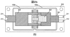
- FIG. 2A and 2B are diagrams showing an example of the configuration of the main part of the power semiconductor module according to the present embodiment.
- FIG. 2A is a cross-sectional view of the power semiconductor module
- FIG. 2B is a plan view of the power semiconductor module.
- the power semiconductor module 500 includes a case 400, a metal base 300, external lead-out terminals 201 to 203, control signal terminals 211 to 214, a circuit board 100, and a solder bonding layer 7.
- the case 400 determines the outer shape of the module and is made of an insulating resin. In the following explanation, explanation of the case is omitted unless particularly necessary.
- the metal base 300 determines the outer shape of the module together with the case 400.
- the metal base 300 is made of a metal material, and dissipates heat generated in one or more circuit boards 100 bonded to the solder bonding layer 7 by contacting the heat radiator. Function as a route to
- External lead-out terminals 201 to 203 are terminals for connecting a metal wiring pattern on the circuit board 100 and a main circuit outside the module, and serve as an input / output path for the energization current of the module.
- the control signal terminals 211 to 214 are terminals for electrically connecting the metal wiring pattern on the circuit board 100 and a control signal generation circuit outside the module via bonding wires 61 to 64, and control signals for the switching elements in the module. It becomes the route.
- the circuit board 100 includes metal wiring patterns 1 to 4, an insulating substrate 5, and a metal wiring pattern 7.
- the number of circuit boards 100 used in the power semiconductor module depends on the function determined by the rated current capacity and the metal wiring pattern. Determined.
- the solder bonding layer 7 mechanically and electrically connects the circuit board 100 and the metal base 300.
- a power semiconductor module is configured by using two circuit boards 100a and 100b.
- the external lead-out terminal 201 is connected to a high-potential metal pattern of the circuit board 100a
- the external lead-out terminal 202 is
- the external lead-out terminal 203 has a function of connecting a low-potential metal pattern of the circuit board 100a and a high-potential metal pattern of the circuit board 100b to the low-potential metal pattern of the circuit board 100b.
- the positions where the high-potential and low-potential external lead-out terminals are connected are arranged close to each other as long as there is no problem in mounting technology and insulation design. This is to minimize the loop area of the path through which the current flows from the high potential metal pattern to the low potential metal pattern, and to suppress the inductance generated in the current path.
- FIG. 3 shows a conventional mounting example of the metal wiring pattern and the semiconductor element on the circuit board 100a.
- the circuit board connects the high-potential metal pattern 1, the low-potential metal pattern 2, the control signal patterns 3 and 4 of the switching semiconductor element, the diode elements 21 to 24 and the switching elements 11 to 16 formed of a semiconductor, and the semiconductor element And bonding wires 31 to 33 and 41 to be formed.
- the metal pattern 1 is electrically connected to the cathode terminals of the diode elements 21 to 24 formed of a semiconductor, and is electrically connected to the collector terminals or drain terminals of the switching elements 11 to 16 formed of a semiconductor. Feeding positions 51 to 52 for connection with the lead-out terminal 201 are arranged.
- Anode terminals of the diode elements 21 to 24 are electrically connected to the metal pattern 2 via bonding wires 41, and collector elements or drain elements of the switching elements 11 to 16 are electrically connected to each other via bonding wires 31.
- feeding positions 53 to 54 for connection to the external lead-out terminal 203 are arranged.
- the gate terminal of the switching element is electrically connected through the bonding wire 32, and is connected to the control signal generating circuit outside the module through the bonding wire 61.
- the source terminal of the switching element is electrically connected through the bonding wire 33, and is connected to the control signal generating circuit outside the module through the bonding wire 62.
- the power feeding positions 51 to 52 and the power feeding positions 51 to 52 of the external lead-out terminals are arranged in the vicinity in order to reduce the inductance of the current path flowing through the circuit board 100a.
- the power semiconductor module of the present invention shown in FIGS. 2a and 2b and the conventional power semiconductor module shown in FIG. 3 are both half-bridge circuits in which the upper arm is constituted by the circuit board 100a and the lower arm is constituted by the circuit board 100b. .
- the external lead-out terminal 201 is a high potential side main terminal
- the external lead-out terminal 202 is a low potential side main terminal
- the external lead-out terminal 203 is an intermediate potential main terminal.
- a circuit board 100a shown in FIG. 3 has power semiconductor elements 11 to 16 mounted on a metal pattern 1, and the metal patterns 2 to 4 connected to the gate terminal and source terminal of the semiconductor element are on the same plane as the metal pattern 1. Is arranged. Since the drain current and the source current of the power semiconductor element flow respectively, the metal patterns 1 and 2 are required to be as wide as possible in order to reduce the parasitic inductance of the path. Further, since the gate terminal wiring and the source (sense) terminal wiring of the power semiconductor element are connected to a plurality of elements, the wiring tends to be long.
- the lengths of the metal pattern 3 and the metal pattern 4 are about 100 mm, and the parasitic inductance generated in these metal patterns is the length.
- the parasitic inductance is as large as 100 nH.
- the area of the metal pattern 1 on which the semiconductor element is mounted is reduced, and the surface mounting efficiency of the power semiconductor element with respect to the circuit board is reduced.
- the proportion of the power semiconductor elements in the area is about 15%.
- the conventional circuit board structure in which the metal patterns shown in FIG. 3 are arranged on the same plane has the following problems 1) and 2).
- 1) The surface mounting efficiency of the power semiconductor element is low, and it is difficult to mount a large number of elements.
- the surface mounting efficiency of the power semiconductor element can be improved by adopting the structure shown in FIG.
- the external dimensions of the circuit board 100a are approximately X on the assumption that the dimensions of the power semiconductor elements of both the diode element and the switching element exemplified in FIG. 3 are equal to each other in the structure of the present invention shown in FIG.
- the size can be reduced to 55 mm in the direction and 32 mm in the Y direction. This is equivalent to improving the surface mounting efficiency of the power semiconductor element, and the ratio can be increased by about 1.5 times to 23%.
- FIG. 1 shows a technique for reducing interference noise generated between these conductors by paying attention to the laminated wiring structure 71 introduced for improving the surface mounting efficiency of the power semiconductor chip, that is, the conductor plate 8 and the metal patterns 3a and 4a. .
- interference noise is due to both magnetic coupling and electric field coupling between two adjacent conductors via an insulating layer.
- interference noise is generated between the conductor plate 8 and the metal patterns 3a and 4a that are close to each other through the insulating plate 9.
- the cause of the magnetic coupling is a mutual inductance M generated between the conductor plate 8 and the metal patterns 3a and 4a. Due to the large mutual inductance M, for example, the change in the source current of the switching elements 11 to 16 flowing through the conductor plate 8 is superimposed on the gate terminal current or the source (sense) terminal current flowing through the metal patterns 3a and 4a. Noise is generated in the voltage between the gate terminal and the source (sense) terminal, which are dominant in characteristics. Due to this noise voltage, there is a possibility that an abnormal operation in which a switching element that is originally in a cutoff (off) state is temporarily turned on (on) may be induced. Therefore, reducing the mutual inductance M, in other words, reducing the coupling coefficient, is essential for reducing the interference noise.
- the cause of electric field coupling is the capacitance between two target conductors.
- parasitic capacitance generated between the conductor plate 8 and the metal pattern 3a that are adjacent to each other via the insulating plate 9 and between the conductor plate 8 and the metal pattern 4a is the cause.
- the parasitic capacitance is inversely proportional to the thickness of the insulating plate 9 and proportional to the areas of the metal patterns 3a and 4a.
- the area of the conductor plate 8 is sufficiently larger than the metal patterns 3a and 4a.
- the width of the conductor plate 8 through which the source currents of the switching elements 11 to 16 and the anode currents of the diode elements 21 to 24 are widened is a practical assumption because it is necessary to reduce the parasitic inductance. In order to reduce the parasitic capacitance, it is necessary to take measures to effectively reduce the facing area of the conductor plate 8 to the metal patterns 3a and 4a.
- the multilayer wiring structure 71 used in the first embodiment by providing a plurality of slit holes 81 in the conductor plate 8, magnetic interference and electric field interference generated between the conductor plate 8 and the metal patterns 3a and 4a are simultaneously reduced.
- a plurality of slit holes 81 are provided in the conductor plate 8, and the longitudinal direction thereof is arranged so as to be orthogonal to the longitudinal direction of the metal patterns 3a and 4a.
- the plurality of slit holes are arranged in the longitudinal direction of the metal patterns 3a and 4a, and the plurality of slit holes are arranged at a constant density in a range where the metal patterns 3a and 4a are projected onto the conductor plate 8.
- the length in the longitudinal direction of the slit hole is selected as long as the slit hole does not reach the collector electrode or drain electrode of the switching elements 11 to 16 connected to the conductor 8.
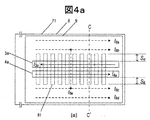
- FIG. 4a shows a schematic diagram of a laminated wiring structure 71 including a conductor plate 8, an insulating plate 9, and metal patterns 3a and 4a.
- Currents flowing through the conductor plate 8 are indicated by dotted lines I8a to I8e, and currents flowing through the metal patterns 3a and 4a are indicated as I3a and I4a.
- I8a to I8e currents flowing through the conductor plate 8
- I3a and I4a currents flowing through the metal patterns 3a and 4a.
- FIG. 4b and FIG. 4c show cross-sectional structures obtained by cutting the structure of FIG. 4a along a line segment C-C '.
- 4B is a cross section when there is no slit hole 81
- FIG. 4C is a cross section when the slit hole 81 is applied (that is, when there is the slit hole 81).
- Sa represents the distance between the conductors 4a and 8 (that is, the shortest distance)
- Sb represents the distance between the conductors 3a and 8 (that is, the shortest distance).
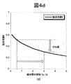
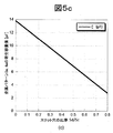
- FIG. 4d is a characteristic diagram showing the relationship between the distances Sa and Sb between the conductors and the coupling coefficient K between the conductors.
- the width of the metal patterns 3a and 4a is 2 mm, and the thickness is negligibly thin.
- the shortest interval between the metal patterns 3a and 4a and the conductor plate 8 is taken on the horizontal axis, and the calculation result of the coupling coefficient K between the conductors arranged at the interval is shown.
- the thickness of the insulating plate 9 is 0.5 mm, this value is the shortest distance between the conductors, and the coupling coefficient K is about 0.52.
- the coupling coefficient K becomes 0.3, and the magnetic coupling can be reduced by about 42%.
- the length of the metal patterns 3a and 4a in the longitudinal direction can be shortened as compared with the configuration of FIG. In the configuration of FIG. 3, it is necessary to arrange all the wiring patterns connected to the power semiconductor elements on the same plane on the insulating plate 5, and the wiring patterns of the metal patterns 3 and 4 connecting the plurality of power semiconductor elements are free. The degree was low and the distance was long.
- the metal patterns 3a and 4a on the laminated wiring structure 71 shown in the first embodiment are arranged on the insulating plate 9 in a plane, the power semiconductor element is not arranged on the plane, so that there are few restrictions on the wiring shape.
- the multilayer wiring structure 71 of Example 1 is effective in reducing noise interference from the viewpoint of shortening the distance between the metal patterns 3a and 4a themselves that receive noise interference.
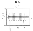
- FIG. 5A is a plan view showing a schematic structure of the multilayer wiring structure 71
- FIG. 5B is a cross-sectional view showing a cross-sectional structure cut along a line segment D-D 'in FIG. 5A. 5a and 5b
- the arrangement pitch distance of the plurality of slit holes 81 is represented by Sc
- the slit hole width (length in the short direction) within the pitch distance Sc is represented by Sd.
- the parasitic capacitance between the metal patterns 3a and 4a and the conductor plate 8 generated through the insulating plate 9 is distributed as shown in the cross-sectional view of FIG.
- the width varies depending on the ratio of the slit hole width Sd to the arrangement pitch distance Sc.
- the insulating plate 9 is made of AlN, and the thickness is 0.5 mm
- the slit hole ratio Sd / Sc and the metal patterns 3a and 4a The calculation result showing the relationship with the parasitic capacitance value is shown in FIG. As the ratio Sd / Sc increases, the parasitic capacitance value decreases. When the ratio Sd / Sc is 0.5, the capacitance value is halved compared to the case where there is no slit hole, as shown in the figure. .
- FIG. 6 is a circuit diagram showing an equivalent circuit of the power semiconductor module according to the present embodiment.
- the effect of the plurality of slit holes 81 arranged in the multilayer wiring structure 71 in the equivalent circuit of FIG. From the description of the circuit board 100 in FIG. 1, for simplification, the parasitic wiring is not shown for the wiring other than the laminated wiring structure 71 and the metal pattern 1, and the metal patterns 3a and 4a are also related to the power semiconductor element.
- the metal pattern 3a is a wiring that connects the gate electrodes of the power semiconductor elements, and the parasitic inductances are indicated by Lg1 and Lg2.
- the metal pattern 4a is a source sense wiring for connecting the source electrode of the power semiconductor element, and its parasitic inductance is indicated by Lss1 and Lss2.
- the conductor plate 8 is a conductor that connects the source electrodes of the power semiconductor elements and allows a source current to flow.
- the parasitic inductance is indicated by Ls1, Ls2, and Ls3.
- the magnetic coupling between the wirings is represented by a coupling coefficient K between the parasitic inductances, the coupling between the metal pattern 3a and the conductor plate 8 is K31 and K32, and the coupling between the metal pattern 4a and the conductor plate 8 is K41. , K42, and the connections between the metal pattern 3a and the metal pattern 4a are KA1, KA2.
- the electric field coupling is equivalently expressed by a parasitic capacitance
- the parasitic capacitance between the metal pattern 3a and the conductor plate 8 is C31, C32, C33
- the parasitic capacitance between the metal pattern 4a and the conductor plate 8 is C41, C42, C43
- the coupling between the metal pattern 3a and the metal pattern 4a is CA1, CA2, and CA3.
- the coupling coefficients K31, K32, K41, and K42 can be reduced by, for example, 42% as described above due to the effect of the plurality of slit holes 81 arranged in the multilayer wiring structure 71.
- this equivalent circuit also shows that the electrical coupling between the conductor plate 8 and the metal patterns 3a and 4a can be reduced, and it is clear that noise interference can be reduced.
- this invention is not limited to the above-mentioned Example, Various modifications are included.
- the above-described embodiments have been described in detail for easy understanding of the present invention, and are not necessarily limited to those having all the configurations described.
- a part of the configuration of one embodiment can be replaced with the configuration of another embodiment, and the configuration of another embodiment can be added to the configuration of one embodiment.
- a MOSFET MOS field effect transistor
- a J-FET junction field effect transistor
- a bipolar device such as an IGBT (insulated gate bipolar transistor)
- the effect of the present invention does not change even if the device is replaced with any one of the above and the terminal functions are replaced with, for example, a drain as a collector, a source as an emitter, and a gate as a base.
- the diode element it goes without saying that the effect of the present invention is not changed by using either a PN junction diode or an SB (Schottky junction) diode.
- wire bond support chips 25 to 26 made of a semiconductor may be used.
- This supporting chip has a chip height similar to that of the semiconductor chips 11 to 16 and 21 to 24, and electrodes are arranged on both surfaces. Therefore, it is possible to connect to the metal pattern 1 and the conductor plate 8 by the same connection method as the semiconductor chips 11 to 16 and 21 to 24. However, insulation between the front and back electrodes can be ensured with a predetermined withstand voltage by the module.
- the support chip is arranged on the back surface at the connection point of the bonding wire to the conductor plate 8 and the connection point of the bonding wire to the conductor patterns 3a and 4a.
- connection site part of the bonding tool is fixed irrespective of the vibration of the said tool. Therefore, according to this configuration, it is possible to prevent the problem that the fixing is insufficient and the vibration of the tool is diffused, and it is possible to secure the bonding wire connection strength.
- This configuration is particularly effective in a situation where the connection site of the bonding tool is easily affected by the vibration of the tool. However, it is needless to say that this supporting chip can be omitted when the connection site is hardly affected by the vibration of the tool by some other means.
- FIG. 7 shows a conductor board 8, an insulating board 9, and control signal conductor patterns 3a and 4a for switching semiconductor elements as circuit boards constituting a power semiconductor module according to Example 2 which is another example of the embodiment of the present invention.
- An example of the circuit board comprised by is shown.
- each of the conductor patterns 3a and 4a is composed of a plurality of sides that intersect at right angles.
- the present embodiment is different from the first embodiment in this point, but the other points are common to the first embodiment.
- the bonding wire connecting between the conductor pattern 3a and the length of the bonding wire connecting the gate electrode of the switching semiconductor element, and connecting the conductor pattern 4a and the source electrode of the switching semiconductor element, respectively. Can be shortened. Thereby, the possibility of resonance in the gate paths of the plurality of switching semiconductor elements can be reduced.
Landscapes
- Engineering & Computer Science (AREA)
- Power Engineering (AREA)
- Physics & Mathematics (AREA)
- Electromagnetism (AREA)
- Inverter Devices (AREA)
Abstract
Description
1)パワー半導体素子の面実装効率が低く、多数の素子の搭載が困難である。
2)素子数が増す場合に、そのゲート端子やソース(センス)端子の接続をおこなう金属パターンの距離が長くなり、面積を占有するとともに、寄生インダクタンスが大きなパターンとなる。
3~4:スイッチング半導体素子の制御信号用導体パターン
5:絶縁基板
7:半田接合層
8:導体板
9:絶縁板
11~16:スイッチング素子
21~24:ダイオード素子
25~26:ワイヤボンド用支持チップ
31~33,41,61~64:ボンディングワイヤ
51~52:外部導出端子201との接続のための給電位置
53~54:外部導出端子203との接続のための給電位置
81,82:スリット孔
100,100a,100b:回路基板
201~203:外部導出端子
211~214:制御信号端子
300:金属ベース300
400:ケース400
500:パワー半導体モジュール
K,K31,K32,K41,K42,KA1,KA2:結合係数
C31~C33,C41~C43,CA1~CA3:寄生容量
Ls1~Ls3,Lss1~Lss2,Lg1~Lg2:寄生インダクタンス
Claims (14)
- 第1の絶縁基板の主面に形成された導体パターンに複数の半導体素子が配置されて成る第1の回路基板を少なくとも1つ以上含み、
前記第1の絶縁基板とは異なる第2の絶縁基板の両面に他の導体パターンが形成されて成る第2の回路基板を少なくとも1つ以上含み、
前記第1の回路基板を構成する前記半導体素子と、前記第2の回路基板を構成する前記他の導体パターンとが互いに接続されて成るパワー半導体モジュールであって、
前記第2の回路基板は、前記他の導体パターン上に、複数の孔状のスリットから成るスリットパターンを有する
ことを特徴とするパワー半導体モジュール。 - 請求項1に記載のパワー半導体モジュールにおいて、
前記複数の半導体素子は少なくとも1つ以上のスイッチング素子を含み、
前記第1の回路基板を構成する前記導体パターンは、
前記第1の絶縁基板上に形成された第1の導体パターンと、
前記第1の絶縁基板上の前記第1の導体パターンとは異なる領域に、前記第1の導体パターンと電気的に絶縁して形成された第2の導体パターンと
を含んで構成され、
前記第1の導体パターンは、その一端に前記第1の導体パターンに電位を供給する第1の給電点を有すると共に、前記第1の導体パターン上に前記少なくとも1つ以上のスイッチング素子の第1の電極端子が接続される構成を有し、
前記第2の導体パターンは、前記第1の給電点の近傍に設けられ、かつ、前記第1の導体パターンとは異なる電位を供給する第2の給電点と、前記第1の導体パターンとは異なる電位を前記第2の回路基板へ供給する第3の給電点とを有し、
前記第2の回路基板を構成する前記他の導体パターンは、
前記第2の絶縁基板上の一方の面に配置された第3の導体パターンと、
前記第2の絶縁基板上であって前記第3の導体パターンが配置された面とは反対側の面に配置された第4の導体パターンおよび第5の導体パターンと
を含んで構成され、
前記第2の回路基板は、前記第3の導体パターンと、前記第4の導体パターンおよび前記第5の導体パターンとを前記第2の絶縁基板によって互いに絶縁する構成を有し、
前記第2の回路基板は、前記第2の回路基板の前記第3の導体パターンが前記第1の回路基板の前記第1の導体パターンと対向するように配置され、
前記第3の導体パターンは、前記少なくとも1つ以上のスイッチング素子の第2の電極端子と接続され、
前記第4の導体パターンは、前記少なくとも1つ以上のスイッチング素子の第2の電極端子と接続され、
前記第5の導体パターンは、前記少なくとも1つ以上のスイッチング素子の第3の電極端子と接続され、
前記第2の導体パターンは、前記第2の回路基板の前記第3の導体パターンと接続され、
前記第1の導体パターンは、前記第1の給電点にて前記パワー半導体モジュールの第1のモジュール電極端子と接続され、
前記第2の導体パターンは、前記第2の給電点および前記第3の給電点の少なくともいずれか一方にて前記パワー半導体モジュールの第2のモジュール電極端子と接続され、
前記第4の導体パターンは、前記第4の導体パターンに電位を供給する第4の給電点を有すると共に、前記第4の給電点にて前記パワー半導体モジュールの第3のモジュール電極端子と接続され、
前記第5の導体パターンは、前記第5の導体パターンに電位を供給する第5の給電点を有すると共に、前記第5の給電点にて前記パワー半導体モジュールの第4のモジュール電極端子と接続され、
前記スリットパターンは、前記第2の回路基板の前記第3の導体パターン、前記第4の導体パターン、および前記第5の導体パターンの少なくともいずれか1つの導体パターン上に形成される
ことを特徴とするパワー半導体モジュール。 - 請求項2に記載のパワー半導体モジュールにおいて、
前記第4の導体パターンの長手方向は、前記第5の導体パターンの長手方向と同一の方向であり、
前記第2の回路基板は、前記第3の導体パターン上に前記スリットパターンを有し、該スリットパターンの長手方向は、前記第4の導体パターンおよび前記第5の導体パターンの長手方向と直交する方向である
ことを特徴とするパワー半導体モジュール。 - 請求項3に記載のパワー半導体モジュールにおいて、
前記第3の導体パターン上に形成された前記スリットパターンは、該スリットパターンを構成する前記複数の孔状のスリットの長手方向が互いに平行である
ことを特徴とするパワー半導体モジュール。 - 請求項4に記載のパワー半導体モジュールにおいて、
前記第4の導体パターンおよび前記第5の導体パターンはそれぞれ、互いに直交する複数の辺によって構成され、
前記第4の導体パターンを構成する各辺の長手方向と前記第5の導体パターンを構成する各辺の長手方向とは、互いに平行であり、かつ、前記第3の導体パターン上に形成された前記スリットパターンを構成する前記複数の孔状のスリットの長手方向と直交する
ことを特徴とするパワー半導体モジュール。 - 請求項5に記載のパワー半導体モジュールにおいて、
前記第2の回路基板の長手方向は、前記第4の導体パターンを構成する各辺および前記第5の導体パターンを構成する各辺のうち最も長い辺の延伸方向と同じ方向であり、
前記第2の回路基板の長手方向は、前記第1の導体パターンの中で電流が最も多く流れる方向に対して直交する方向である
ことを特徴とするパワー半導体モジュール。 - 請求項2乃至6のいずれか1項に記載のパワー半導体モジュールにおいて、
前記複数の半導体素子は少なくとも1つ以上のダイオード素子を更に含み、
前記第1の導体パターン上に、前記少なくとも1つ以上のダイオード素子の第1の電極端子が接続され、
前記第3の導体パターン上に、前記少なくとも1つ以上のダイオード素子の第2の電極端子が接続される
ことを特徴とするパワー半導体モジュール。 - 請求項7に記載のパワー半導体モジュールにおいて、
前記少なくとも1つ以上のスイッチング素子の第1の電極端子はドレイン電極もしくはコレクタ電極であり、
前記少なくとも1つ以上のスイッチング素子の第2の電極端子はソース電極もしくはエミッタ電極であり、
前記少なくとも1つ以上のスイッチング素子の第3の電極端子はゲート電極であり、
前記少なくとも1つ以上のダイオード素子の第1の電極端子はカソード電極であり、
前記少なくとも1つ以上のダイオード素子の第2の電極端子はアノード電極である
ことを特徴とするパワー半導体モジュール。 - 請求項7または8に記載のパワー半導体モジュールにおいて、
前記第2の回路基板の前記第3の導体パターンは、前記少なくとも1つ以上のスイッチング素子の第2の電極端子および前記の少なくとも1つ以上のダイオード素子の第2の電極端子に対して半田で接続される
ことを特徴とするパワー半導体モジュール。 - 請求項2乃至9のいずれか1項に記載のパワー半導体モジュールにおいて、
前記第2の回路基板の前記第4の導体パターンと前記第5の導体パターンとの電位差に基づいて前記少なくとも1つ以上のスイッチング素子のスイッチ状態が制御される
ことを特徴とするパワー半導体モジュール。 - 請求項2乃至10のいずれか1項に記載のパワー半導体モジュールにおいて、
前記第2の回路基板の前記第4の導体パターンは、前記少なくとも1つ以上のスイッチング素子の第3の電極端子とワイヤボンディングによって接続され、
前記第2の回路基板の前記第5の導体パターンは、前記少なくとも1つ以上のスイッチング素子の第2の電極端子とワイヤボンディングによって接続される
ことを特徴とするパワー半導体モジュール。 - 請求項2乃至11のいずれか1項に記載のパワー半導体モジュールにおいて、
前記第3の導体パターンと、前記第2の導体パターンの前記第3の給電点とは、ボンディングワイヤによって互いに接続される
ことを特徴とするパワー半導体モジュール。 - 請求項12に記載のパワー半導体モジュールにおいて、
前記第3の導体パターン上の前記ボンディングワイヤの接続点の近傍には、前記第3の導体パターンと前記第1の導体パターンとの間を互いに絶縁するダミー半導体チップが配置される
ことを特徴とするパワー半導体モジュール。 - 請求項2乃至13のいずれか1項に記載のパワー半導体モジュールにおいて、
前記第4の導体パターンと前記第3のモジュール電極端子とは、ボンディングワイヤによって互いに接続され、
前記第5の導体パターンと前記第4のモジュール電極端子とは、ボンディングワイヤによって互いに接続される
ことを特徴とするパワー半導体モジュール。
Priority Applications (2)
| Application Number | Priority Date | Filing Date | Title |
|---|---|---|---|
| JP2018507090A JP6623283B2 (ja) | 2016-03-24 | 2017-01-31 | パワー半導体モジュール |
| EP17769659.8A EP3442020B1 (en) | 2016-03-24 | 2017-01-31 | Power semiconductor module |
Applications Claiming Priority (2)
| Application Number | Priority Date | Filing Date | Title |
|---|---|---|---|
| JP2016059387 | 2016-03-24 | ||
| JP2016-059387 | 2016-03-24 |
Publications (1)
| Publication Number | Publication Date |
|---|---|
| WO2017163612A1 true WO2017163612A1 (ja) | 2017-09-28 |
Family
ID=59901115
Family Applications (1)
| Application Number | Title | Priority Date | Filing Date |
|---|---|---|---|
| PCT/JP2017/003255 Ceased WO2017163612A1 (ja) | 2016-03-24 | 2017-01-31 | パワー半導体モジュール |
Country Status (3)
| Country | Link |
|---|---|
| EP (1) | EP3442020B1 (ja) |
| JP (1) | JP6623283B2 (ja) |
| WO (1) | WO2017163612A1 (ja) |
Cited By (13)
| Publication number | Priority date | Publication date | Assignee | Title |
|---|---|---|---|---|
| CN107958905A (zh) * | 2017-12-11 | 2018-04-24 | 臻驱科技(上海)有限公司 | 功率半导体模块衬底 |
| WO2019167418A1 (ja) * | 2018-03-01 | 2019-09-06 | パナソニックIpマネジメント株式会社 | ロボット |
| JP2020047656A (ja) * | 2018-09-14 | 2020-03-26 | 富士電機株式会社 | 半導体ユニット、半導体モジュール及び半導体装置 |
| CN111162069A (zh) * | 2019-12-23 | 2020-05-15 | 广东美的白色家电技术创新中心有限公司 | 一种智能功率模块及其制备方法 |
| CN113097082A (zh) * | 2021-03-31 | 2021-07-09 | 重庆线易电子科技有限责任公司 | 一种数字隔离器与键合线焊接方法 |
| JP2021141665A (ja) * | 2020-03-03 | 2021-09-16 | 大光電機株式会社 | オフライン用照明器具 |
| US11398450B2 (en) | 2020-03-06 | 2022-07-26 | Fuji Electric Co., Ltd. | Semiconductor module |
| US11418003B2 (en) * | 2018-06-07 | 2022-08-16 | Ii-Vi Delaware, Inc. | Chip on carrier |
| CN115692370A (zh) * | 2022-11-11 | 2023-02-03 | 蜂巢传动系统(江苏)有限公司保定研发分公司 | 功率模块及具有其的车辆 |
| WO2023042482A1 (ja) * | 2021-09-17 | 2023-03-23 | 株式会社日立パワーデバイス | パワー半導体モジュールおよび電力変換装置 |
| US11742333B2 (en) | 2020-03-27 | 2023-08-29 | Fuji Electric Co., Ltd. | Semiconductor module |
| DE112023000179T5 (de) | 2022-04-13 | 2024-04-25 | Fuji Electric Co., Ltd. | Halbleitervorrichtung |
| CN119833507A (zh) * | 2024-12-30 | 2025-04-15 | 西安交通大学 | 一种低电感碳化硅功率模块与换流回路结构 |
Citations (7)
| Publication number | Priority date | Publication date | Assignee | Title |
|---|---|---|---|---|
| JPH10309073A (ja) * | 1997-03-07 | 1998-11-17 | Hitachi Ltd | 電力変換器およびその製造方法 |
| JP3096721U (ja) * | 2003-03-06 | 2003-10-03 | 立衛科技股▲ふん▼有限公司 | 積層構造を有するパッケージ構造 |
| JP2005026524A (ja) * | 2003-07-03 | 2005-01-27 | Fuji Electric Device Technology Co Ltd | 半導体装置及びその製造方法 |
| JP2007173680A (ja) * | 2005-12-26 | 2007-07-05 | Denso Corp | 半導体装置 |
| JP2010258135A (ja) * | 2009-04-23 | 2010-11-11 | Nippon Soken Inc | 電力変換用半導体装置 |
| JP2013033812A (ja) * | 2011-08-01 | 2013-02-14 | Fuji Electric Co Ltd | パワー半導体モジュール |
| WO2016009496A1 (ja) * | 2014-07-15 | 2016-01-21 | 株式会社日立製作所 | パワートランジスタモジュール |
Family Cites Families (2)
| Publication number | Priority date | Publication date | Assignee | Title |
|---|---|---|---|---|
| JPH10308471A (ja) * | 1997-05-07 | 1998-11-17 | Akita Denshi Kk | 混成集積回路装置およびその製造方法 |
| KR100780692B1 (ko) * | 2006-03-29 | 2007-11-30 | 주식회사 하이닉스반도체 | 칩 스택 패키지 |
-
2017
- 2017-01-31 WO PCT/JP2017/003255 patent/WO2017163612A1/ja not_active Ceased
- 2017-01-31 EP EP17769659.8A patent/EP3442020B1/en active Active
- 2017-01-31 JP JP2018507090A patent/JP6623283B2/ja active Active
Patent Citations (7)
| Publication number | Priority date | Publication date | Assignee | Title |
|---|---|---|---|---|
| JPH10309073A (ja) * | 1997-03-07 | 1998-11-17 | Hitachi Ltd | 電力変換器およびその製造方法 |
| JP3096721U (ja) * | 2003-03-06 | 2003-10-03 | 立衛科技股▲ふん▼有限公司 | 積層構造を有するパッケージ構造 |
| JP2005026524A (ja) * | 2003-07-03 | 2005-01-27 | Fuji Electric Device Technology Co Ltd | 半導体装置及びその製造方法 |
| JP2007173680A (ja) * | 2005-12-26 | 2007-07-05 | Denso Corp | 半導体装置 |
| JP2010258135A (ja) * | 2009-04-23 | 2010-11-11 | Nippon Soken Inc | 電力変換用半導体装置 |
| JP2013033812A (ja) * | 2011-08-01 | 2013-02-14 | Fuji Electric Co Ltd | パワー半導体モジュール |
| WO2016009496A1 (ja) * | 2014-07-15 | 2016-01-21 | 株式会社日立製作所 | パワートランジスタモジュール |
Cited By (19)
| Publication number | Priority date | Publication date | Assignee | Title |
|---|---|---|---|---|
| CN107958905A (zh) * | 2017-12-11 | 2018-04-24 | 臻驱科技(上海)有限公司 | 功率半导体模块衬底 |
| WO2019167418A1 (ja) * | 2018-03-01 | 2019-09-06 | パナソニックIpマネジメント株式会社 | ロボット |
| US11418003B2 (en) * | 2018-06-07 | 2022-08-16 | Ii-Vi Delaware, Inc. | Chip on carrier |
| JP2020047656A (ja) * | 2018-09-14 | 2020-03-26 | 富士電機株式会社 | 半導体ユニット、半導体モジュール及び半導体装置 |
| JP7172326B2 (ja) | 2018-09-14 | 2022-11-16 | 富士電機株式会社 | 半導体ユニット、半導体モジュール及び半導体装置 |
| CN111162069A (zh) * | 2019-12-23 | 2020-05-15 | 广东美的白色家电技术创新中心有限公司 | 一种智能功率模块及其制备方法 |
| JP2021141665A (ja) * | 2020-03-03 | 2021-09-16 | 大光電機株式会社 | オフライン用照明器具 |
| JP7449722B2 (ja) | 2020-03-03 | 2024-03-14 | 大光電機株式会社 | オフライン用照明器具 |
| US11398450B2 (en) | 2020-03-06 | 2022-07-26 | Fuji Electric Co., Ltd. | Semiconductor module |
| US11742333B2 (en) | 2020-03-27 | 2023-08-29 | Fuji Electric Co., Ltd. | Semiconductor module |
| US12469826B2 (en) | 2020-03-27 | 2025-11-11 | Fuji Electric Co., Ltd. | Semiconductor module |
| CN113097082A (zh) * | 2021-03-31 | 2021-07-09 | 重庆线易电子科技有限责任公司 | 一种数字隔离器与键合线焊接方法 |
| CN113097082B (zh) * | 2021-03-31 | 2023-05-16 | 重庆线易电子科技有限责任公司 | 一种数字隔离器与键合线焊接方法 |
| JP2023044542A (ja) * | 2021-09-17 | 2023-03-30 | 株式会社 日立パワーデバイス | パワー半導体モジュールおよび電力変換装置 |
| WO2023042482A1 (ja) * | 2021-09-17 | 2023-03-23 | 株式会社日立パワーデバイス | パワー半導体モジュールおよび電力変換装置 |
| JP7593573B2 (ja) | 2021-09-17 | 2024-12-03 | ミネベアパワーデバイス株式会社 | パワー半導体モジュールおよび電力変換装置 |
| DE112023000179T5 (de) | 2022-04-13 | 2024-04-25 | Fuji Electric Co., Ltd. | Halbleitervorrichtung |
| CN115692370A (zh) * | 2022-11-11 | 2023-02-03 | 蜂巢传动系统(江苏)有限公司保定研发分公司 | 功率模块及具有其的车辆 |
| CN119833507A (zh) * | 2024-12-30 | 2025-04-15 | 西安交通大学 | 一种低电感碳化硅功率模块与换流回路结构 |
Also Published As
| Publication number | Publication date |
|---|---|
| JP6623283B2 (ja) | 2019-12-18 |
| JPWO2017163612A1 (ja) | 2018-09-27 |
| EP3442020A1 (en) | 2019-02-13 |
| EP3442020A4 (en) | 2019-12-04 |
| EP3442020B1 (en) | 2020-10-07 |
Similar Documents
| Publication | Publication Date | Title |
|---|---|---|
| JP6623283B2 (ja) | パワー半導体モジュール | |
| US9659912B2 (en) | Low-inductance circuit arrangement comprising load current collecting conductor track | |
| JP5550553B2 (ja) | 電力用半導体モジュール | |
| CN103051312B (zh) | 低阻抗栅极控制方法和设备 | |
| JP6405383B2 (ja) | パワートランジスタモジュール | |
| JP6400201B2 (ja) | パワー半導体モジュール | |
| US12087752B2 (en) | Semiconductor module | |
| CN109997223B (zh) | 功率半导体模块 | |
| CN104380463B (zh) | 用于将多个功率晶体管安装在其上的衬底和功率半导体模块 | |
| JPWO2014185050A1 (ja) | 半導体装置 | |
| US9768100B1 (en) | Semiconductor device | |
| JP2015018943A (ja) | パワー半導体モジュールおよびそれを用いた電力変換装置 | |
| NL2021292B1 (en) | Electronic module | |
| US20220139797A1 (en) | Semiconductor module, power semiconductor module, and power electronic equipment using the semiconductor module or the power semiconductor module | |
| US7821128B2 (en) | Power semiconductor device having lines within a housing | |
| US9655265B2 (en) | Electronic module | |
| US10530354B2 (en) | Insulated gate semiconductor device and method for manufacturing insulated gate semiconductor device | |
| JP4142539B2 (ja) | 電力用半導体装置 | |
| JP5801339B2 (ja) | 半導体装置 | |
| JP6394459B2 (ja) | 半導体装置 | |
| JP2014063806A (ja) | 半導体装置 | |
| US20240363497A1 (en) | Semiconductor module arrangements | |
| US20260047461A1 (en) | Semiconductor module | |
| WO2026083476A1 (ja) | パワーモジュール | |
| JP2023060675A (ja) | 半導体装置およびそれを用いた電力変換装置 |
Legal Events
| Date | Code | Title | Description |
|---|---|---|---|
| ENP | Entry into the national phase |
Ref document number: 2018507090 Country of ref document: JP Kind code of ref document: A |
|
| WWE | Wipo information: entry into national phase |
Ref document number: 2017769659 Country of ref document: EP |
|
| ENP | Entry into the national phase |
Ref document number: 2017769659 Country of ref document: EP Effective date: 20181024 |
|
| 121 | Ep: the epo has been informed by wipo that ep was designated in this application |
Ref document number: 17769659 Country of ref document: EP Kind code of ref document: A1 |