WO2017163669A1 - Corps stratifié, procédé de production d'un substrat doté d'une couche plaquée à motifs, procédé de production d'un corps stratifié contenant une couche métallique, et capteur de panneau tactile ainsi que panneau tactile - Google Patents
Corps stratifié, procédé de production d'un substrat doté d'une couche plaquée à motifs, procédé de production d'un corps stratifié contenant une couche métallique, et capteur de panneau tactile ainsi que panneau tactile Download PDFInfo
- Publication number
- WO2017163669A1 WO2017163669A1 PCT/JP2017/005269 JP2017005269W WO2017163669A1 WO 2017163669 A1 WO2017163669 A1 WO 2017163669A1 JP 2017005269 W JP2017005269 W JP 2017005269W WO 2017163669 A1 WO2017163669 A1 WO 2017163669A1
- Authority
- WO
- WIPO (PCT)
- Prior art keywords
- layer
- plated
- substrate
- group
- protective film
- Prior art date
- Legal status (The legal status is an assumption and is not a legal conclusion. Google has not performed a legal analysis and makes no representation as to the accuracy of the status listed.)
- Ceased
Links
Images



Classifications
-
- B—PERFORMING OPERATIONS; TRANSPORTING
- B32—LAYERED PRODUCTS
- B32B—LAYERED PRODUCTS, i.e. PRODUCTS BUILT-UP OF STRATA OF FLAT OR NON-FLAT, e.g. CELLULAR OR HONEYCOMB, FORM
- B32B27/00—Layered products comprising a layer of synthetic resin
- B32B27/28—Layered products comprising a layer of synthetic resin comprising synthetic resins not wholly covered by any one of the sub-groups B32B27/30 - B32B27/42
-
- B—PERFORMING OPERATIONS; TRANSPORTING
- B32—LAYERED PRODUCTS
- B32B—LAYERED PRODUCTS, i.e. PRODUCTS BUILT-UP OF STRATA OF FLAT OR NON-FLAT, e.g. CELLULAR OR HONEYCOMB, FORM
- B32B27/00—Layered products comprising a layer of synthetic resin
- B32B27/06—Layered products comprising a layer of synthetic resin as the main or only constituent of a layer, which is next to another layer of the same or of a different material
- B32B27/08—Layered products comprising a layer of synthetic resin as the main or only constituent of a layer, which is next to another layer of the same or of a different material of synthetic resin
-
- B—PERFORMING OPERATIONS; TRANSPORTING
- B32—LAYERED PRODUCTS
- B32B—LAYERED PRODUCTS, i.e. PRODUCTS BUILT-UP OF STRATA OF FLAT OR NON-FLAT, e.g. CELLULAR OR HONEYCOMB, FORM
- B32B17/00—Layered products essentially comprising sheet glass, or glass, slag, or like fibres
- B32B17/06—Layered products essentially comprising sheet glass, or glass, slag, or like fibres comprising glass as the main or only constituent of a layer, next to another layer of a specific material
-
- B—PERFORMING OPERATIONS; TRANSPORTING
- B32—LAYERED PRODUCTS
- B32B—LAYERED PRODUCTS, i.e. PRODUCTS BUILT-UP OF STRATA OF FLAT OR NON-FLAT, e.g. CELLULAR OR HONEYCOMB, FORM
- B32B23/00—Layered products comprising a layer of cellulosic plastic substances, i.e. substances obtained by chemical modification of cellulose, e.g. cellulose ethers, cellulose esters, viscose
- B32B23/04—Layered products comprising a layer of cellulosic plastic substances, i.e. substances obtained by chemical modification of cellulose, e.g. cellulose ethers, cellulose esters, viscose comprising such cellulosic plastic substance as the main or only constituent of a layer, which is next to another layer of the same or of a different material
- B32B23/08—Layered products comprising a layer of cellulosic plastic substances, i.e. substances obtained by chemical modification of cellulose, e.g. cellulose ethers, cellulose esters, viscose comprising such cellulosic plastic substance as the main or only constituent of a layer, which is next to another layer of the same or of a different material of synthetic resin
-
- B—PERFORMING OPERATIONS; TRANSPORTING
- B32—LAYERED PRODUCTS
- B32B—LAYERED PRODUCTS, i.e. PRODUCTS BUILT-UP OF STRATA OF FLAT OR NON-FLAT, e.g. CELLULAR OR HONEYCOMB, FORM
- B32B27/00—Layered products comprising a layer of synthetic resin
-
- B—PERFORMING OPERATIONS; TRANSPORTING
- B32—LAYERED PRODUCTS
- B32B—LAYERED PRODUCTS, i.e. PRODUCTS BUILT-UP OF STRATA OF FLAT OR NON-FLAT, e.g. CELLULAR OR HONEYCOMB, FORM
- B32B27/00—Layered products comprising a layer of synthetic resin
- B32B27/18—Layered products comprising a layer of synthetic resin characterised by the use of special additives
-
- B—PERFORMING OPERATIONS; TRANSPORTING
- B32—LAYERED PRODUCTS
- B32B—LAYERED PRODUCTS, i.e. PRODUCTS BUILT-UP OF STRATA OF FLAT OR NON-FLAT, e.g. CELLULAR OR HONEYCOMB, FORM
- B32B27/00—Layered products comprising a layer of synthetic resin
- B32B27/28—Layered products comprising a layer of synthetic resin comprising synthetic resins not wholly covered by any one of the sub-groups B32B27/30 - B32B27/42
- B32B27/285—Layered products comprising a layer of synthetic resin comprising synthetic resins not wholly covered by any one of the sub-groups B32B27/30 - B32B27/42 comprising polyethers
-
- B—PERFORMING OPERATIONS; TRANSPORTING
- B32—LAYERED PRODUCTS
- B32B—LAYERED PRODUCTS, i.e. PRODUCTS BUILT-UP OF STRATA OF FLAT OR NON-FLAT, e.g. CELLULAR OR HONEYCOMB, FORM
- B32B27/00—Layered products comprising a layer of synthetic resin
- B32B27/28—Layered products comprising a layer of synthetic resin comprising synthetic resins not wholly covered by any one of the sub-groups B32B27/30 - B32B27/42
- B32B27/286—Layered products comprising a layer of synthetic resin comprising synthetic resins not wholly covered by any one of the sub-groups B32B27/30 - B32B27/42 comprising polysulphones; polysulfides
-
- B—PERFORMING OPERATIONS; TRANSPORTING
- B32—LAYERED PRODUCTS
- B32B—LAYERED PRODUCTS, i.e. PRODUCTS BUILT-UP OF STRATA OF FLAT OR NON-FLAT, e.g. CELLULAR OR HONEYCOMB, FORM
- B32B27/00—Layered products comprising a layer of synthetic resin
- B32B27/30—Layered products comprising a layer of synthetic resin comprising vinyl (co)polymers; comprising acrylic (co)polymers
- B32B27/304—Layered products comprising a layer of synthetic resin comprising vinyl (co)polymers; comprising acrylic (co)polymers comprising vinyl halide (co)polymers, e.g. PVC, PVDC, PVF, PVDF
-
- B—PERFORMING OPERATIONS; TRANSPORTING
- B32—LAYERED PRODUCTS
- B32B—LAYERED PRODUCTS, i.e. PRODUCTS BUILT-UP OF STRATA OF FLAT OR NON-FLAT, e.g. CELLULAR OR HONEYCOMB, FORM
- B32B27/00—Layered products comprising a layer of synthetic resin
- B32B27/30—Layered products comprising a layer of synthetic resin comprising vinyl (co)polymers; comprising acrylic (co)polymers
- B32B27/308—Layered products comprising a layer of synthetic resin comprising vinyl (co)polymers; comprising acrylic (co)polymers comprising acrylic (co)polymers
-
- B—PERFORMING OPERATIONS; TRANSPORTING
- B32—LAYERED PRODUCTS
- B32B—LAYERED PRODUCTS, i.e. PRODUCTS BUILT-UP OF STRATA OF FLAT OR NON-FLAT, e.g. CELLULAR OR HONEYCOMB, FORM
- B32B27/00—Layered products comprising a layer of synthetic resin
- B32B27/32—Layered products comprising a layer of synthetic resin comprising polyolefins
-
- B—PERFORMING OPERATIONS; TRANSPORTING
- B32—LAYERED PRODUCTS
- B32B—LAYERED PRODUCTS, i.e. PRODUCTS BUILT-UP OF STRATA OF FLAT OR NON-FLAT, e.g. CELLULAR OR HONEYCOMB, FORM
- B32B27/00—Layered products comprising a layer of synthetic resin
- B32B27/32—Layered products comprising a layer of synthetic resin comprising polyolefins
- B32B27/325—Layered products comprising a layer of synthetic resin comprising polyolefins comprising polycycloolefins
-
- B—PERFORMING OPERATIONS; TRANSPORTING
- B32—LAYERED PRODUCTS
- B32B—LAYERED PRODUCTS, i.e. PRODUCTS BUILT-UP OF STRATA OF FLAT OR NON-FLAT, e.g. CELLULAR OR HONEYCOMB, FORM
- B32B27/00—Layered products comprising a layer of synthetic resin
- B32B27/34—Layered products comprising a layer of synthetic resin comprising polyamides
-
- B—PERFORMING OPERATIONS; TRANSPORTING
- B32—LAYERED PRODUCTS
- B32B—LAYERED PRODUCTS, i.e. PRODUCTS BUILT-UP OF STRATA OF FLAT OR NON-FLAT, e.g. CELLULAR OR HONEYCOMB, FORM
- B32B27/00—Layered products comprising a layer of synthetic resin
- B32B27/36—Layered products comprising a layer of synthetic resin comprising polyesters
-
- B—PERFORMING OPERATIONS; TRANSPORTING
- B32—LAYERED PRODUCTS
- B32B—LAYERED PRODUCTS, i.e. PRODUCTS BUILT-UP OF STRATA OF FLAT OR NON-FLAT, e.g. CELLULAR OR HONEYCOMB, FORM
- B32B27/00—Layered products comprising a layer of synthetic resin
- B32B27/36—Layered products comprising a layer of synthetic resin comprising polyesters
- B32B27/365—Layered products comprising a layer of synthetic resin comprising polyesters comprising polycarbonates
-
- B—PERFORMING OPERATIONS; TRANSPORTING
- B32—LAYERED PRODUCTS
- B32B—LAYERED PRODUCTS, i.e. PRODUCTS BUILT-UP OF STRATA OF FLAT OR NON-FLAT, e.g. CELLULAR OR HONEYCOMB, FORM
- B32B27/00—Layered products comprising a layer of synthetic resin
- B32B27/40—Layered products comprising a layer of synthetic resin comprising polyurethanes
-
- B—PERFORMING OPERATIONS; TRANSPORTING
- B32—LAYERED PRODUCTS
- B32B—LAYERED PRODUCTS, i.e. PRODUCTS BUILT-UP OF STRATA OF FLAT OR NON-FLAT, e.g. CELLULAR OR HONEYCOMB, FORM
- B32B7/00—Layered products characterised by the relation between layers; Layered products characterised by the relative orientation of features between layers, or by the relative values of a measurable parameter between layers, i.e. products comprising layers having different physical, chemical or physicochemical properties; Layered products characterised by the interconnection of layers
- B32B7/04—Interconnection of layers
- B32B7/06—Interconnection of layers permitting easy separation
-
- B—PERFORMING OPERATIONS; TRANSPORTING
- B32—LAYERED PRODUCTS
- B32B—LAYERED PRODUCTS, i.e. PRODUCTS BUILT-UP OF STRATA OF FLAT OR NON-FLAT, e.g. CELLULAR OR HONEYCOMB, FORM
- B32B7/00—Layered products characterised by the relation between layers; Layered products characterised by the relative orientation of features between layers, or by the relative values of a measurable parameter between layers, i.e. products comprising layers having different physical, chemical or physicochemical properties; Layered products characterised by the interconnection of layers
- B32B7/04—Interconnection of layers
- B32B7/12—Interconnection of layers using interposed adhesives or interposed materials with bonding properties
-
- B—PERFORMING OPERATIONS; TRANSPORTING
- B32—LAYERED PRODUCTS
- B32B—LAYERED PRODUCTS, i.e. PRODUCTS BUILT-UP OF STRATA OF FLAT OR NON-FLAT, e.g. CELLULAR OR HONEYCOMB, FORM
- B32B9/00—Layered products comprising a layer of a particular substance not covered by groups B32B11/00 - B32B29/00
- B32B9/005—Layered products comprising a layer of a particular substance not covered by groups B32B11/00 - B32B29/00 comprising one layer of ceramic material, e.g. porcelain, ceramic tile
-
- B—PERFORMING OPERATIONS; TRANSPORTING
- B32—LAYERED PRODUCTS
- B32B—LAYERED PRODUCTS, i.e. PRODUCTS BUILT-UP OF STRATA OF FLAT OR NON-FLAT, e.g. CELLULAR OR HONEYCOMB, FORM
- B32B9/00—Layered products comprising a layer of a particular substance not covered by groups B32B11/00 - B32B29/00
- B32B9/04—Layered products comprising a layer of a particular substance not covered by groups B32B11/00 - B32B29/00 comprising such particular substance as the main or only constituent of a layer, which is next to another layer of the same or of a different material
- B32B9/045—Layered products comprising a layer of a particular substance not covered by groups B32B11/00 - B32B29/00 comprising such particular substance as the main or only constituent of a layer, which is next to another layer of the same or of a different material of synthetic resin
-
- C—CHEMISTRY; METALLURGY
- C08—ORGANIC MACROMOLECULAR COMPOUNDS; THEIR PREPARATION OR CHEMICAL WORKING-UP; COMPOSITIONS BASED THEREON
- C08J—WORKING-UP; GENERAL PROCESSES OF COMPOUNDING; AFTER-TREATMENT NOT COVERED BY SUBCLASSES C08B, C08C, C08F, C08G or C08H
- C08J5/00—Manufacture of articles or shaped materials containing macromolecular substances
- C08J5/18—Manufacture of films or sheets
-
- C—CHEMISTRY; METALLURGY
- C08—ORGANIC MACROMOLECULAR COMPOUNDS; THEIR PREPARATION OR CHEMICAL WORKING-UP; COMPOSITIONS BASED THEREON
- C08J—WORKING-UP; GENERAL PROCESSES OF COMPOUNDING; AFTER-TREATMENT NOT COVERED BY SUBCLASSES C08B, C08C, C08F, C08G or C08H
- C08J7/00—Chemical treatment or coating of shaped articles made of macromolecular substances
- C08J7/04—Coating
- C08J7/042—Coating with two or more layers, where at least one layer of a composition contains a polymer binder
- C08J7/0423—Coating with two or more layers, where at least one layer of a composition contains a polymer binder with at least one layer of inorganic material and at least one layer of a composition containing a polymer binder
-
- C—CHEMISTRY; METALLURGY
- C08—ORGANIC MACROMOLECULAR COMPOUNDS; THEIR PREPARATION OR CHEMICAL WORKING-UP; COMPOSITIONS BASED THEREON
- C08J—WORKING-UP; GENERAL PROCESSES OF COMPOUNDING; AFTER-TREATMENT NOT COVERED BY SUBCLASSES C08B, C08C, C08F, C08G or C08H
- C08J7/00—Chemical treatment or coating of shaped articles made of macromolecular substances
- C08J7/04—Coating
- C08J7/043—Improving the adhesiveness of the coatings per se, e.g. forming primers
-
- C—CHEMISTRY; METALLURGY
- C08—ORGANIC MACROMOLECULAR COMPOUNDS; THEIR PREPARATION OR CHEMICAL WORKING-UP; COMPOSITIONS BASED THEREON
- C08J—WORKING-UP; GENERAL PROCESSES OF COMPOUNDING; AFTER-TREATMENT NOT COVERED BY SUBCLASSES C08B, C08C, C08F, C08G or C08H
- C08J7/00—Chemical treatment or coating of shaped articles made of macromolecular substances
- C08J7/04—Coating
- C08J7/046—Forming abrasion-resistant coatings; Forming surface-hardening coatings
-
- C—CHEMISTRY; METALLURGY
- C08—ORGANIC MACROMOLECULAR COMPOUNDS; THEIR PREPARATION OR CHEMICAL WORKING-UP; COMPOSITIONS BASED THEREON
- C08L—COMPOSITIONS OF MACROMOLECULAR COMPOUNDS
- C08L67/00—Compositions of polyesters obtained by reactions forming a carboxylic ester link in the main chain; Compositions of derivatives of such polymers
- C08L67/02—Polyesters derived from dicarboxylic acids and dihydroxy compounds
-
- C—CHEMISTRY; METALLURGY
- C08—ORGANIC MACROMOLECULAR COMPOUNDS; THEIR PREPARATION OR CHEMICAL WORKING-UP; COMPOSITIONS BASED THEREON
- C08L—COMPOSITIONS OF MACROMOLECULAR COMPOUNDS
- C08L69/00—Compositions of polycarbonates; Compositions of derivatives of polycarbonates
-
- G—PHYSICS
- G03—PHOTOGRAPHY; CINEMATOGRAPHY; ANALOGOUS TECHNIQUES USING WAVES OTHER THAN OPTICAL WAVES; ELECTROGRAPHY; HOLOGRAPHY
- G03F—PHOTOMECHANICAL PRODUCTION OF TEXTURED OR PATTERNED SURFACES, e.g. FOR PRINTING, FOR PROCESSING OF SEMICONDUCTOR DEVICES; MATERIALS THEREFOR; ORIGINALS THEREFOR; APPARATUS SPECIALLY ADAPTED THEREFOR
- G03F7/00—Photomechanical, e.g. photolithographic, production of textured or patterned surfaces, e.g. printing surfaces; Materials therefor, e.g. comprising photoresists; Apparatus specially adapted therefor
- G03F7/004—Photosensitive materials
- G03F7/027—Non-macromolecular photopolymerisable compounds having carbon-to-carbon double bonds, e.g. ethylenic compounds
-
- G—PHYSICS
- G03—PHOTOGRAPHY; CINEMATOGRAPHY; ANALOGOUS TECHNIQUES USING WAVES OTHER THAN OPTICAL WAVES; ELECTROGRAPHY; HOLOGRAPHY
- G03F—PHOTOMECHANICAL PRODUCTION OF TEXTURED OR PATTERNED SURFACES, e.g. FOR PRINTING, FOR PROCESSING OF SEMICONDUCTOR DEVICES; MATERIALS THEREFOR; ORIGINALS THEREFOR; APPARATUS SPECIALLY ADAPTED THEREFOR
- G03F7/00—Photomechanical, e.g. photolithographic, production of textured or patterned surfaces, e.g. printing surfaces; Materials therefor, e.g. comprising photoresists; Apparatus specially adapted therefor
- G03F7/004—Photosensitive materials
- G03F7/027—Non-macromolecular photopolymerisable compounds having carbon-to-carbon double bonds, e.g. ethylenic compounds
- G03F7/032—Non-macromolecular photopolymerisable compounds having carbon-to-carbon double bonds, e.g. ethylenic compounds with binders
- G03F7/033—Non-macromolecular photopolymerisable compounds having carbon-to-carbon double bonds, e.g. ethylenic compounds with binders the binders being polymers obtained by reactions only involving carbon-to-carbon unsaturated bonds, e.g. vinyl polymers
-
- G—PHYSICS
- G03—PHOTOGRAPHY; CINEMATOGRAPHY; ANALOGOUS TECHNIQUES USING WAVES OTHER THAN OPTICAL WAVES; ELECTROGRAPHY; HOLOGRAPHY
- G03F—PHOTOMECHANICAL PRODUCTION OF TEXTURED OR PATTERNED SURFACES, e.g. FOR PRINTING, FOR PROCESSING OF SEMICONDUCTOR DEVICES; MATERIALS THEREFOR; ORIGINALS THEREFOR; APPARATUS SPECIALLY ADAPTED THEREFOR
- G03F7/00—Photomechanical, e.g. photolithographic, production of textured or patterned surfaces, e.g. printing surfaces; Materials therefor, e.g. comprising photoresists; Apparatus specially adapted therefor
- G03F7/004—Photosensitive materials
- G03F7/038—Macromolecular compounds which are rendered insoluble or differentially wettable
- G03F7/0388—Macromolecular compounds which are rendered insoluble or differentially wettable with ethylenic or acetylenic bands in the side chains of the photopolymer
-
- G—PHYSICS
- G03—PHOTOGRAPHY; CINEMATOGRAPHY; ANALOGOUS TECHNIQUES USING WAVES OTHER THAN OPTICAL WAVES; ELECTROGRAPHY; HOLOGRAPHY
- G03F—PHOTOMECHANICAL PRODUCTION OF TEXTURED OR PATTERNED SURFACES, e.g. FOR PRINTING, FOR PROCESSING OF SEMICONDUCTOR DEVICES; MATERIALS THEREFOR; ORIGINALS THEREFOR; APPARATUS SPECIALLY ADAPTED THEREFOR
- G03F7/00—Photomechanical, e.g. photolithographic, production of textured or patterned surfaces, e.g. printing surfaces; Materials therefor, e.g. comprising photoresists; Apparatus specially adapted therefor
- G03F7/004—Photosensitive materials
- G03F7/09—Photosensitive materials characterised by structural details, e.g. supports, auxiliary layers
- G03F7/11—Photosensitive materials characterised by structural details, e.g. supports, auxiliary layers having cover layers or intermediate layers, e.g. subbing layers
-
- G—PHYSICS
- G06—COMPUTING OR CALCULATING; COUNTING
- G06F—ELECTRIC DIGITAL DATA PROCESSING
- G06F3/00—Input arrangements for transferring data to be processed into a form capable of being handled by the computer; Output arrangements for transferring data from processing unit to output unit, e.g. interface arrangements
- G06F3/01—Input arrangements or combined input and output arrangements for interaction between user and computer
- G06F3/03—Arrangements for converting the position or the displacement of a member into a coded form
- G06F3/041—Digitisers, e.g. for touch screens or touch pads, characterised by the transducing means
- G06F3/044—Digitisers, e.g. for touch screens or touch pads, characterised by the transducing means by capacitive means
-
- B—PERFORMING OPERATIONS; TRANSPORTING
- B32—LAYERED PRODUCTS
- B32B—LAYERED PRODUCTS, i.e. PRODUCTS BUILT-UP OF STRATA OF FLAT OR NON-FLAT, e.g. CELLULAR OR HONEYCOMB, FORM
- B32B2255/00—Coating on the layer surface
- B32B2255/10—Coating on the layer surface on synthetic resin layer or on natural or synthetic rubber layer
-
- B—PERFORMING OPERATIONS; TRANSPORTING
- B32—LAYERED PRODUCTS
- B32B—LAYERED PRODUCTS, i.e. PRODUCTS BUILT-UP OF STRATA OF FLAT OR NON-FLAT, e.g. CELLULAR OR HONEYCOMB, FORM
- B32B2255/00—Coating on the layer surface
- B32B2255/20—Inorganic coating
- B32B2255/205—Metallic coating
-
- B—PERFORMING OPERATIONS; TRANSPORTING
- B32—LAYERED PRODUCTS
- B32B—LAYERED PRODUCTS, i.e. PRODUCTS BUILT-UP OF STRATA OF FLAT OR NON-FLAT, e.g. CELLULAR OR HONEYCOMB, FORM
- B32B2255/00—Coating on the layer surface
- B32B2255/26—Polymeric coating
-
- B—PERFORMING OPERATIONS; TRANSPORTING
- B32—LAYERED PRODUCTS
- B32B—LAYERED PRODUCTS, i.e. PRODUCTS BUILT-UP OF STRATA OF FLAT OR NON-FLAT, e.g. CELLULAR OR HONEYCOMB, FORM
- B32B2255/00—Coating on the layer surface
- B32B2255/28—Multiple coating on one surface
-
- B—PERFORMING OPERATIONS; TRANSPORTING
- B32—LAYERED PRODUCTS
- B32B—LAYERED PRODUCTS, i.e. PRODUCTS BUILT-UP OF STRATA OF FLAT OR NON-FLAT, e.g. CELLULAR OR HONEYCOMB, FORM
- B32B2307/00—Properties of the layers or laminate
- B32B2307/20—Properties of the layers or laminate having particular electrical or magnetic properties, e.g. piezoelectric
- B32B2307/202—Conductive
-
- B—PERFORMING OPERATIONS; TRANSPORTING
- B32—LAYERED PRODUCTS
- B32B—LAYERED PRODUCTS, i.e. PRODUCTS BUILT-UP OF STRATA OF FLAT OR NON-FLAT, e.g. CELLULAR OR HONEYCOMB, FORM
- B32B2307/00—Properties of the layers or laminate
- B32B2307/70—Other properties
- B32B2307/732—Dimensional properties
-
- B—PERFORMING OPERATIONS; TRANSPORTING
- B32—LAYERED PRODUCTS
- B32B—LAYERED PRODUCTS, i.e. PRODUCTS BUILT-UP OF STRATA OF FLAT OR NON-FLAT, e.g. CELLULAR OR HONEYCOMB, FORM
- B32B2307/00—Properties of the layers or laminate
- B32B2307/70—Other properties
- B32B2307/748—Releasability
-
- B—PERFORMING OPERATIONS; TRANSPORTING
- B32—LAYERED PRODUCTS
- B32B—LAYERED PRODUCTS, i.e. PRODUCTS BUILT-UP OF STRATA OF FLAT OR NON-FLAT, e.g. CELLULAR OR HONEYCOMB, FORM
- B32B2367/00—Polyesters, e.g. PET, i.e. polyethylene terephthalate
-
- B—PERFORMING OPERATIONS; TRANSPORTING
- B32—LAYERED PRODUCTS
- B32B—LAYERED PRODUCTS, i.e. PRODUCTS BUILT-UP OF STRATA OF FLAT OR NON-FLAT, e.g. CELLULAR OR HONEYCOMB, FORM
- B32B2369/00—Polycarbonates
-
- B—PERFORMING OPERATIONS; TRANSPORTING
- B32—LAYERED PRODUCTS
- B32B—LAYERED PRODUCTS, i.e. PRODUCTS BUILT-UP OF STRATA OF FLAT OR NON-FLAT, e.g. CELLULAR OR HONEYCOMB, FORM
- B32B2457/00—Electrical equipment
- B32B2457/08—PCBs, i.e. printed circuit boards
-
- B—PERFORMING OPERATIONS; TRANSPORTING
- B32—LAYERED PRODUCTS
- B32B—LAYERED PRODUCTS, i.e. PRODUCTS BUILT-UP OF STRATA OF FLAT OR NON-FLAT, e.g. CELLULAR OR HONEYCOMB, FORM
- B32B2457/00—Electrical equipment
- B32B2457/14—Semiconductor wafers
-
- B—PERFORMING OPERATIONS; TRANSPORTING
- B32—LAYERED PRODUCTS
- B32B—LAYERED PRODUCTS, i.e. PRODUCTS BUILT-UP OF STRATA OF FLAT OR NON-FLAT, e.g. CELLULAR OR HONEYCOMB, FORM
- B32B2457/00—Electrical equipment
- B32B2457/20—Displays, e.g. liquid crystal displays, plasma displays
- B32B2457/202—LCD, i.e. liquid crystal displays
-
- B—PERFORMING OPERATIONS; TRANSPORTING
- B32—LAYERED PRODUCTS
- B32B—LAYERED PRODUCTS, i.e. PRODUCTS BUILT-UP OF STRATA OF FLAT OR NON-FLAT, e.g. CELLULAR OR HONEYCOMB, FORM
- B32B2457/00—Electrical equipment
- B32B2457/20—Displays, e.g. liquid crystal displays, plasma displays
- B32B2457/206—Organic displays, e.g. OLED
-
- B—PERFORMING OPERATIONS; TRANSPORTING
- B32—LAYERED PRODUCTS
- B32B—LAYERED PRODUCTS, i.e. PRODUCTS BUILT-UP OF STRATA OF FLAT OR NON-FLAT, e.g. CELLULAR OR HONEYCOMB, FORM
- B32B2457/00—Electrical equipment
- B32B2457/20—Displays, e.g. liquid crystal displays, plasma displays
- B32B2457/208—Touch screens
-
- C—CHEMISTRY; METALLURGY
- C08—ORGANIC MACROMOLECULAR COMPOUNDS; THEIR PREPARATION OR CHEMICAL WORKING-UP; COMPOSITIONS BASED THEREON
- C08J—WORKING-UP; GENERAL PROCESSES OF COMPOUNDING; AFTER-TREATMENT NOT COVERED BY SUBCLASSES C08B, C08C, C08F, C08G or C08H
- C08J2367/00—Characterised by the use of polyesters obtained by reactions forming a carboxylic ester link in the main chain; Derivatives of such polymers
- C08J2367/02—Polyesters derived from dicarboxylic acids and dihydroxy compounds
-
- C—CHEMISTRY; METALLURGY
- C08—ORGANIC MACROMOLECULAR COMPOUNDS; THEIR PREPARATION OR CHEMICAL WORKING-UP; COMPOSITIONS BASED THEREON
- C08J—WORKING-UP; GENERAL PROCESSES OF COMPOUNDING; AFTER-TREATMENT NOT COVERED BY SUBCLASSES C08B, C08C, C08F, C08G or C08H
- C08J2433/00—Characterised by the use of homopolymers or copolymers of compounds having one or more unsaturated aliphatic radicals, each having only one carbon-to-carbon double bond, and only one being terminated by only one carboxyl radical, or of salts, anhydrides, esters, amides, imides, or nitriles thereof; Derivatives of such polymers
- C08J2433/04—Characterised by the use of homopolymers or copolymers of compounds having one or more unsaturated aliphatic radicals, each having only one carbon-to-carbon double bond, and only one being terminated by only one carboxyl radical, or of salts, anhydrides, esters, amides, imides, or nitriles thereof; Derivatives of such polymers esters
- C08J2433/14—Characterised by the use of homopolymers or copolymers of compounds having one or more unsaturated aliphatic radicals, each having only one carbon-to-carbon double bond, and only one being terminated by only one carboxyl radical, or of salts, anhydrides, esters, amides, imides, or nitriles thereof; Derivatives of such polymers esters of esters containing halogen, nitrogen, sulfur, or oxygen atoms in addition to the carboxy oxygen
Definitions
- the present invention relates to a laminate, a method of manufacturing a substrate with a pattern-like layer to be plated, a method of manufacturing a metal layer-containing laminate, a touch panel sensor, and a touch panel.
- Patent Document 1 describes “a composition for forming a layer to be plated, which contains a polymer containing a non-dissociative functional group which forms an interaction with a plating catalyst or a precursor thereof, a radically polymerizable group, and an ionic polar group”.
- the to-be-plated layer which can be developed by aqueous solution and has the outstanding adsorption property with respect to a plating catalyst or its precursor can be formed. Moreover, according to the method for producing a metal pattern material described in Patent Document 1, a metal pattern excellent in adhesion to a substrate can be easily formed using development with an aqueous solution.
- the metal wiring pattern of the obtained metal layer-containing laminate will be thicker than the opening pattern of the photomask ( It has also been found that a new problem of pattern thickening occurs.
- this invention makes it a subject to provide the laminated body which can obtain the metal layer containing laminated body in which generation
- Another object of the present invention is to provide a substrate with a pattern-like layer to be plated, a method for producing a metal layer-containing laminate, and a touch panel sensor and a touch panel.
- the inventor of the present invention is a laminate including a substrate, a layer to be plated, and a temporary protective film in this order, which is a substrate and a layer to be plated It has been found that the above problems can be solved by controlling the light absorption properties of the polymerization initiator and the temporary protective film contained in the above. That is, it discovered that the said objective could be achieved by the following structures.
- the layer to be plated layer formation contains a polymerization initiator and the following compound X or composition Y, An absorption edge ⁇ 0 on the long wavelength side of the UV-visible absorption spectrum of the temporary protective film, An absorption edge ⁇ 1 on the long wavelength side of the UV-visible absorption spectrum of the polymerization initiator,
- fills the relationship represented by the following formula (Z).
- a step of irradiating light to the layer to be plated in a pattern from the temporary protective film side in the laminate according to any one of [1] to [5], and for forming the layer to be plated The step of removing the temporary protective film on the layer, the step of removing the area not irradiated with light in the layer to be plated formation, and forming the pattern-like layer to be plated on the substrate Applying a plating catalyst or a precursor thereof to the layer, performing a plating treatment on the pattern-like to-be-plated layer to which the plating catalyst or its precursor is applied, and forming a metal layer on the pattern-like to-be-plated layer And a method for producing a metal layer-containing laminate.
- a touch panel sensor comprising the metal layer-containing laminate obtained by the manufacturing method according to [7].
- a metal layer-containing laminate in which the occurrence of pattern thickening is suppressed (hereinafter also referred to as “having the effect of the present invention”), and a laminate can be provided. Furthermore, according to the present invention, it is possible to provide a substrate with a pattern-like layer to be plated, a method for producing a metal layer-containing laminate, a touch panel sensor and a touch panel.
- a numerical range represented using “to” means a range including numerical values described before and after “to” as the lower limit value and the upper limit value.
- the laminate according to the first embodiment of the present invention is a laminate including a substrate, a layer for forming a layer to be plated, and a temporary protective film in this order, and the layer for forming a layer to be plated starts polymerization.
- the following compound X or composition Y, the absorption edge ⁇ 0 of the long wavelength side of the UV-visible absorption spectrum of the temporary protective film, and the absorption edge ⁇ of the long wavelength side of the UV-visible absorption spectrum of the polymerization initiator 1 and a long wavelength side absorption end ⁇ 2 of the UV-visible absorption spectrum of the substrate satisfy the relationship represented by the following formula (Z).
- the unit of each absorption end is nm.
- Compound X a compound containing a functional group that interacts with a plating catalyst or its precursor, and a polymerizable group.
- Composition Y A composition containing a functional group capable of interacting with a plating catalyst or its precursor, and a compound containing a polymerizable group.
- One of the features of the laminate is that the light absorption characteristics of the substrate, the polymerization initiator contained in the layer to be plated, and the temporary protective film are controlled.
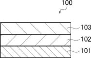
- FIG. 1 is a cross-sectional view of a laminate according to the first embodiment.
- the laminated body 100 which concerns on this embodiment contains the board
- the photomask When a photomask is disposed on the temporary protective film side of the laminate and light is irradiated in a pattern, the photomask does not directly contact the laminate. Therefore, since the transfer of the component does not occur between the two and / or the photomask is not contaminated with the component of the layer to be plated, the yield of the patterned substrate with the layer to be plated is improved.
- FIG. 1 is a cross-sectional view of a laminate according to the first embodiment.
- the laminated body 100 which concerns on this embodiment contains the board
- the photomask does not directly contact the laminate. Therefore, since the transfer of the
- FIG. 2 is a cross-sectional view when a photomask 201 is disposed on the temporary protective film 103 side of the stack and light is irradiated in a pattern. Arrows in the figure schematically represent light irradiation.
- the light irradiated to the temporary protective film 103 passes through the temporary protective film 103, reaches the layer to be plated formation 102, and sensitizes a polymerization initiator (not shown). Part of the light that has reached the layer-to-be-plated layer formation 102 passes through the layer-to-be-plated layer formation 102 and reaches the substrate 101.
- the temporary protective film 103 is disposed between the photomask 201 and the layer 102 for forming a layer to be plated (the temporary protective film 103 is provided on the layer 102 for forming a layer to be plated).
- the light irradiated via the photomask 201 is scattered by a minute. When this light reaches the substrate 101, it is presumed that the light is scattered at the interface of the substrate 101 and is incident on the layer 102 for plating layer formation again. Thereby, it is estimated that the photosensitive region of the layer 102 for to-be-plated layer formation will spread more than a desired pattern shape. When the photosensitive region is expanded, wiring thickening occurs in the metal layer-containing laminate obtained thereby.
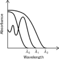
- the absorption edge lambda 0 of the long wavelength side of the ultraviolet-visible absorption spectrum of the temporary protective film the absorption of the long wavelength side of the ultraviolet-visible absorption spectrum of the polymerization initiator contained in the layer to be plated layer formed
- the end ⁇ 1 and the absorption end ⁇ 2 on the long wavelength side of the UV-visible absorption spectrum of the substrate satisfy the relationship represented by the following formula (Z).
- the relationship between ⁇ 0 , ⁇ 1 and ⁇ 2 is shown in FIG. Formula (Z) ⁇ 0 ⁇ 1 ⁇ 2
- the light of the wavelength region which is not absorbed by the temporary protective film can sensitize the polymerization initiator.
- Substrate is not particularly limited as long as the absorption edge lambda 2 on the long wavelength side of the ultraviolet visible absorption spectrum of the substrate satisfy a relation represented by the above formula (Z), among others, an insulating substrate, more Specifically, a substrate made of resin (hereinafter, also referred to as “resin substrate”), a ceramic substrate, a glass substrate or the like can be used, and a resin substrate is more preferable. In addition, the following adhesive sheets are also included in the resin substrate.
- the material of the resin substrate is not particularly limited, but a resin containing an aromatic group in that the absorption end ⁇ 2 on the long wavelength side of the UV-visible absorption spectrum of the substrate can easily satisfy the relationship represented by the above formula (Z). It is preferred to include a P 1. And it comprises an aromatic group is intended to include aromatic groups in the structural unit of the resin P 1.
- the aromatic group is not particularly limited.
- polyester resin polyethylene terephthalate, polyethylene naphthalate
- polyethersulfone resin polyacrylic resin, polyurethane resin, polycarbonate resin, polysulfone resin, polyamide resin, polyarylate
- system resins polyolefin resins, cellulose resins, polyvinyl chloride resins, and cycloolefin resins.
- polyethylene terephthalate, polyethylene naphthalate, polyolefin or polycarbonate is preferable, and it is preferable to include at least one selected from the group consisting of polyethylene terephthalate and polycarbonate from the viewpoint of high light transmittance and excellent mechanical properties.
- polyethylene terephthalate PolyEthylene Terephthalate (hereinafter, also simply referred to as "PET") or polycarbonate is more preferable, and polyethylene terephthalate is even more preferable.
- an adhesive substrate that is, an adhesive sheet may be used.
- Well-known materials acrylic pressure sensitive adhesive, silicone pressure sensitive adhesive, etc. can be used as a material which constitutes an adhesive sheet.
- the thickness (mm) of the substrate is not particularly limited, but is preferably 0.01 to 2 mm, more preferably 0.02 to 1 mm, and more preferably 0.03 to 0.1 mm for the resin substrate from the viewpoint of balance between handleability and thinning. Is more preferred.
- the thickness is preferably 0.01 to 2 mm, more preferably 0.3 to 0.8 mm, and still more preferably 0.4 to 0.7 mm.
- the substrate preferably transmits light appropriately. Specifically, the total light transmittance of the substrate is preferably 85 to 100%.
- the absorption edge ⁇ 2 on the long wavelength side of the UV-visible absorption spectrum of the substrate is not particularly limited as long as the relationship represented by the above formula (1) is satisfied, but the transparency of the substrate with a pattern-like layer to be formed and From the viewpoint of excellent visibility, the thickness is preferably 400 nm or less, more preferably 380 nm or less, and still more preferably 320 nm or less.
- the lower limit is not particularly limited, but is often 250 nm or more in terms of material properties.
- the position of the absorption edge of the UV-visible absorption spectrum of the substrate usually depends on the material of the substrate.
- the absorption edge lambda 2 on the long wavelength side of the ultraviolet visible absorption spectrum of the substrate the ultraviolet visible absorption spectrum of the substrate when measured at UV-3000 (Shimadzu Corporation), the most absorbance of 1.0 or less Intended for the longer wavelength side.
- the substrate may contain an ultraviolet absorber.
- the inclusion of ultraviolet absorbers in the substrate move absorption edge lambda 2 of ultraviolet-visible absorption spectrum of the substrate is more to the long wavelength side, easily satisfy the relation represented by the above formula (Z).
- the substrate and the following temporary protective film are the same material, it is preferable that the substrate contains an ultraviolet absorber.
- the substrate is preferably made of PET containing an ultraviolet absorber.
- an ultraviolet absorber it is preferable to select the ultraviolet absorber which has an absorption edge in the long wavelength side rather than absorption edge (lambda) 1 of the long wavelength side of the ultraviolet visible absorption spectrum of a polymerization initiator.
- the absorption edge on the longer wavelength side of the ultraviolet-visible absorption spectrum of the ultraviolet absorber used is, than the absorption edge lambda 1 of the long wavelength side of the ultraviolet-visible absorption spectrum of the polymerization initiator is preferably in the long wavelength side.
- the procedure similar to the above is mentioned also as the measuring method of the absorption edge of the ultraviolet visible absorption spectrum of the board
- UV absorber to be used is not particularly limited, and known UV absorbers can be used.
- salicylic acid UV absorber for example, salicylic acid UV absorber, benzophenone UV absorber, benzotriazole UV absorber, cyanoacrylate UV absorber And benzoate based ultraviolet light absorbers, malonic acid ester based ultraviolet light absorbers, and oxalic acid anilide based ultraviolet light absorbers.
- salicylic acid ultraviolet absorber include phenyl salicylate, p-tert-butylphenyl salicylate, and p-octylphenyl salicylate.
- benzophenone-based UV absorbers examples include 2,4-dihydroxybenzophenone, 2-hydroxy-4-methoxybenzophenone, 2-hydroxy-4-octoxybenzophenone, 2-hydroxy-4-dodecyloxybenzophenone, and 2,2'-.
- the content of the ultraviolet absorber is not particularly limited, but is preferably 0.01 to 20 parts by mass, and more preferably 0.1 to 10 parts by mass with respect to 100 parts by mass of the total mass of the substrate.
- the substrate has more excellent ultraviolet absorptivity, and the ultraviolet absorber is less likely to be deposited on the substrate surface.
- the substrate may have a single layer structure or a multilayer structure.
- the substrate includes a laminate including a support and an ultraviolet absorbing layer containing an ultraviolet absorber disposed on the support.
- the support may or may not contain the ultraviolet light absorber, and the type thereof includes those exemplified as the above-mentioned substrate.
- the ultraviolet absorbing layer contains at least an ultraviolet absorber. As an ultraviolet absorber, those mentioned above are mentioned.
- binders, such as resin, may be contained in the ultraviolet absorber.
- the layer to be plated layer formation is a layer to be a plated layer by the following light irradiation, and contains at least a polymerization initiator and the following compound X or composition Y. More specifically, the layer to be plated layer forming may be a layer containing a polymerization initiator and the compound X or a layer containing a polymerization initiator and the composition Y.
- Compound X a compound containing a functional group that interacts with a plating catalyst or a precursor thereof (hereinafter, also simply referred to as an “interactive group”), and a polymerizable group.
- Composition Y A composition containing a functional group capable of interacting with a plating catalyst or its precursor, and a compound containing a polymerizable group.
- the polymerization initiator is not particularly limited, as long as the absorption end ⁇ 1 on the long wavelength side of the UV-visible absorption spectrum of the polymerization initiator satisfies the relationship represented by the formula (Z), a known polymerization initiator (so-called light A polymerization initiator) etc. can be used.
- polymerization initiators examples include benzophenones, acetophenones, ⁇ -aminoalkylphenones, benzoins, ketones, thioxanthones, benzyls, benzil ketals, oxsim esters, ansolones, tetramethylthiuram monosulfide And bisacyl phosphinoxides, acyl phosphine oxides, anthraquinones, azo compounds, etc., and derivatives thereof.
- the polymerization initiator may be used alone or in combination of two or more.
- the absorption edge lambda 1 of ultraviolet-visible absorption spectrum of a polymerization initiator (as a solvent, solvent polymerization initiator is dissolved, for example, using acetonitrile) polymerization initiator concentration of 0.01 mass% solution
- the wavelength on the side of the longest wavelength at which the absorbance is 1.0 or less is intended.
- the absorption edge lambda 1 of the long wavelength side of the ultraviolet-visible absorption spectrum of the polymerization initiator, ultraviolet temporary protective film absorption edge lambda 2 and below the long wavelength side of the ultraviolet visible absorption spectrum of the substrate may be satisfied in relation to the absorption edge ⁇ 0 on the long wavelength side of the visible absorption spectrum.
- Formula (Z) ⁇ 0 ⁇ 1 ⁇ 2 The difference between ⁇ 2 and ⁇ 1 is preferably 4 nm or more, more preferably 5 nm or more, and still more preferably 10 nm or more in that light is easily absorbed by the substrate.
- the upper limit is not particularly limited, but is often about 150 nm.
- the absorption edge at the long wavelength side of the ultraviolet-visible absorption spectrum of the polymerization initiator having the absorption edge at the long wavelength side of the ultraviolet-visible absorption spectrum at the longer wavelength side Let ⁇ be ⁇ 1 .
- the content of the polymerization initiator in the layer to be plated layer formation is not particularly limited, it is from 0.01 to 5% by mass with respect to the total mass of the layer to be plated layer formation in terms of the curability of the layer to be plated. And preferably 0.1 to 3% by mass.
- the compound X is a compound containing an interactive group and a polymerizable group.
- the interactive group intends a functional group capable of interacting with the plating catalyst or its precursor applied to the pattern-like plating layer, and for example, a functional group capable of forming an electrostatic interaction with the plating catalyst or its precursor
- a nitrogen-containing functional group, a sulfur-containing functional group, an oxygen-containing functional group or the like which can form a coordinate with a group, or a plating catalyst or a precursor thereof can be used.
- salts thereof can also be used.
- ionic polar groups such as carboxylic acid groups, sulfonic acid groups, phosphoric acid groups, and boronic acid groups, ether groups, or the like because they have high polarity and high adsorption ability to a plating catalyst or a precursor thereof, etc.
- a cyano group is preferred, and a carboxylic acid group or a cyano group is more preferred.
- the compound X may contain two or more interactive groups.
- the compound X may be a low molecular weight compound or a high molecular weight compound.
- the low molecular weight compound intends a compound having a molecular weight of less than 1000
- the high molecular weight compound intends a compound having a molecular weight of 1000 or more.
- the low molecular weight compound containing the said polymeric group corresponds to what is called a monomer (monomer).
- the polymer compound may be a polymer containing a predetermined repeating unit.
- only 1 type may be used and 2 or more types may be used together.
- the weight-average molecular weight of the polymer is not particularly limited, but is preferably 1000 or more and 700,000 or less, and more preferably 2000 or more and 200,000 or less in terms of high solubility and more excellent handleability. In particular, from the viewpoint of polymerization sensitivity, 20000 or more is more preferable.
- the synthesis method of the polymer containing such a polymerizable group and the interaction group is not particularly limited, and known synthesis methods (see paragraphs [0097] to [0125] of patent publication 2009-280905) are used. .
- a repeating unit containing a polymerizable group represented by the following formula (a) (hereinafter appropriately referred to as a polymerizable group unit), and a mutual represented by the following formula (b)
- a copolymer containing a repeating unit containing a functional group (hereinafter also referred to as an interactive group unit as appropriate) can be mentioned.
- R 1 to R 5 each independently represent a hydrogen atom or a substituted or unsubstituted alkyl group (eg, methyl group, ethyl group, propyl group or butyl group) Group etc.).
- the type of substituent is not particularly limited, and examples thereof include a methoxy group, a chlorine atom, a bromine atom, and a fluorine atom.
- R 1 a hydrogen atom, a methyl group or a methyl group substituted with a bromine atom is preferable.
- R 2 a hydrogen atom, a methyl group or a methyl group substituted with a bromine atom is preferable.
- R 3 a hydrogen atom is preferable.
- R 4 a hydrogen atom is preferable.
- R 5 a hydrogen atom, a methyl group or a methyl group substituted with a bromine atom is preferable.
- X, Y and Z each independently represent a single bond or a substituted or unsubstituted divalent organic group.
- divalent organic group a substituted or unsubstituted divalent aliphatic hydrocarbon group (preferably having a carbon number of 1 to 8; for example, an alkylene group such as a methylene group, an ethylene group or a propylene group), a substituted or non-substituted Substituted divalent aromatic hydrocarbon group (preferably having a carbon number of 6 to 12.
- phenylene group For example, phenylene group), -O-, -S-, -SO 2- , -N (R)-(R: alkyl group) And -CO-, -NH-, -COO-, -CONH-, or a combination thereof (eg, an alkyleneoxy group, an alkylene carbonyloxy group, an alkylene carbonyloxy group, etc.) and the like.
- a single bond, an ester group (-COO-), an amide group (-CONH-), an ether group are easy to synthesize a polymer, and the adhesion of the following metal layer is more excellent.
- (-O-) or a substituted or unsubstituted divalent aromatic hydrocarbon group is preferable, and a single bond, an ester group (-COO-) or an amido group (-CONH-) is more preferable.
- L 1 and L 2 each independently represent a single bond or a substituted or unsubstituted divalent organic group.
- the definition of the divalent organic group is the same as the divalent organic group described above for X, Y, and Z.
- L 1 an aliphatic hydrocarbon group or a divalent organic group containing a urethane bond or a urea bond (for example, an aliphatic hydrocarbon) in that the synthesis of the polymer is easy and the adhesion of the metal layer is more excellent Group is preferable, and those having 1 to 9 carbon atoms in total are more preferable.
- the total number of carbon atoms of L 1 means the total number of carbon atoms contained in the divalent organic group or a substituted or unsubstituted represented by L 1.
- L 2 is a single bond, a divalent aliphatic hydrocarbon group, a divalent aromatic hydrocarbon group, or a combination thereof in that the adhesion of the metal layer is more excellent.
- L 2 is more preferably a single bond or a total of 1 to 15 carbon atoms.
- the divalent organic group represented by L 2 is preferably unsubstituted.
- the total number of carbon atoms of L 2 means the total number of carbon atoms contained in the divalent organic group or a substituted or unsubstituted represented by L 2.
- W represents an interactive group.
- the definition of the interactive group is as described above.
- the content of the polymerizable group unit is 5 to 50% by mole based on all repeating units in the polymer from the viewpoint of reactivity (curability and / or polymerization) and suppression of gelation in synthesis. Preferably, 5 to 40 mol% is more preferable. Further, the content of the above-mentioned interactive group unit is preferably 5 to 95 mol%, more preferably 10 to 95 mol%, with respect to all repeating units in the polymer from the viewpoint of adsorption to the plating catalyst or its precursor. More preferable.
- the repeating unit represented by Formula (A) is the same as the repeating unit represented by said Formula (a), and description of each group is also the same.
- R 5, X and L 2 in the repeating unit represented by formula (B) is the same as R 5, X and L 2 in the repeating unit represented by formula (b), a description of each group Is also the same.
- Wa in Formula (B) represents a group that interacts with the plating catalyst or the precursor thereof, excluding the hydrophilic group represented by V below or the precursor group thereof. Among these, a cyano group or an ether group is preferable.
- each R 6 independently represents a hydrogen atom or a substituted or unsubstituted alkyl group.
- U represents a single bond or a substituted or unsubstituted divalent organic group.
- the definition of the divalent organic group is the same as the divalent organic group represented by X, Y and Z described above.
- U the synthesis of the polymer is easy and the adhesion of the metal layer is more excellent, and a single bond, an ester group (-COO-), an amide group (-CONH-), an ether group (-O-), or Preferred is a substituted or unsubstituted divalent aromatic hydrocarbon group.
- L 3 represents a single bond or a substituted or unsubstituted divalent organic group.
- the definition of the divalent organic group is the same as the divalent organic group represented by L 1 and L 2 described above.
- L 3 a single bond or a divalent aliphatic hydrocarbon group, a divalent aromatic hydrocarbon group, or a combination thereof is used in that the polymer synthesis is easy and the adhesion of the metal layer is more excellent. Is preferred.
- V represents a hydrophilic group or a precursor group thereof.
- the hydrophilic group is not particularly limited as long as it is a group exhibiting hydrophilicity, and examples thereof include a hydroxyl group and a carboxylic acid group.
- a precursor group of a hydrophilic group means a group which generates a hydrophilic group by a predetermined treatment (for example, treatment with an acid or an alkali), for example, THP (2-tetrahydropyranyl group: 2-tetrahydropyranyl group) And the like.
- the hydrophilic group is preferably an ionic polar group in terms of interaction with the plating catalyst or the precursor thereof.
- the ionic polar group examples include a carboxylic acid group, a sulfonic acid group, a phosphoric acid group, and a boronic acid group.
- a carboxylic acid group is preferable from the viewpoint of appropriate acidity (does not decompose other functional groups).
- the preferred content of each unit in the second preferred embodiment of the above-mentioned polymer is as follows.
- the content of the repeating unit represented by the formula (A) is 5 for all repeating units in the polymer from the viewpoint of reactivity (curability and / or polymerization) and suppression of gelation during synthesis. -50 mol% is preferable, and 5 to 30 mol% is more preferable.
- the content of the repeating unit represented by the formula (B) is preferably 5 to 75 mol%, more preferably 10 to 70 mol, based on all the repeating units in the polymer, from the viewpoint of adsorption to the plating catalyst or its precursor. % Is more preferable.
- the content of the repeating unit represented by the formula (C) is preferably 10 to 70% by mole, and more preferably 20 to 60% by mole, based on all repeating units in the polymer, from the viewpoint of developability with wet solution and moisture adhesion. Is more preferable, and 30 to 50 mol% is more preferable.
- This polymer can be produced by known methods, such as those in the literature listed above.
- R 11 to R 13 each independently represent a hydrogen atom or a substituted or unsubstituted alkyl group.
- the unsubstituted alkyl group include a methyl group, an ethyl group, a propyl group or a butyl group.
- a substituted alkyl group a methyl group, an ethyl group, a propyl group, and a butyl group substituted by the methoxy group, a chlorine atom, a bromine atom, or a fluorine atom etc. are mentioned.
- R 11 a hydrogen atom or a methyl group is preferable.
- R 12 a hydrogen atom is preferable.
- R 13 a hydrogen atom is preferable.
- L 10 represents a single bond or a divalent organic group.
- a divalent organic group a substituted or unsubstituted aliphatic hydrocarbon group (preferably having a carbon number of 1 to 8), a substituted or unsubstituted aromatic hydrocarbon group (preferably having a carbon number of 6 to 12), -O -, -S-, -SO 2- , -N (R)-(R: alkyl group), -CO-, -NH-, -COO-, -CONH-, and a combination thereof (eg, alkylene An oxy group, an alkylene carbonyloxy group, an alkylene carbonyloxy group etc. etc. are mentioned.
- a substituted or unsubstituted aliphatic hydrocarbon group a methylene group, an ethylene group, a propylene group, or a butylene group, or these groups are substituted by a methoxy group, a chlorine atom, a bromine atom, or a fluorine atom etc. Is preferred.
- the substituted or unsubstituted aromatic hydrocarbon group an unsubstituted phenylene group or a phenylene group substituted with a methoxy group, a chlorine atom, a bromine atom, a fluorine atom or the like is preferable.
- one of the preferred embodiments of L 10 includes —NH—aliphatic hydrocarbon group— or —CO—aliphatic hydrocarbon group—.
- W is the same as the definition of W in Formula (b), and represents an interactive group.
- the definition of the interactive group is as described above.
- Formula (X) as a preferable aspect of W, an ionic polar group is mentioned, and a carboxylic acid group is more preferable.
- Composition Y is a composition containing a compound containing an interactive group and a compound containing a polymerizable group. That is, the to-be-plated layer forming layer contains two types of a compound containing an interactive group and a compound containing a polymerizable group.
- the definition of the interactive group and the polymerizable group is as described above.
- the compound containing an interactive group may be a low molecular weight compound or a high molecular weight compound.
- the polymer for example, polyacrylic acid
- a polymerizable group is not contained in the compound containing an interactive group.
- the compound containing a polymerizable group is a so-called monomer, and is preferably a polyfunctional monomer containing two or more polymerizable groups in that the hardness of the layer to be plated to be formed is more excellent.
- the polyfunctional monomer it is preferable to use a monomer containing 2 to 6 polymerizable groups.
- the molecular weight of the polyfunctional monomer to be used is preferably 150 to 1000, more preferably 200 to 700, from the viewpoint of molecular mobility during the crosslinking reaction that affects the reactivity.
- the distance (distance) between the plurality of polymerizable groups is preferably 1 to 15 in terms of the number of atoms, and more preferably 6 or more and 10 or less.
- the compound containing a polymerizable group may contain an interactive group.
- R 20 represents a polymerizable group.
- L represents a single bond or a divalent organic group.
- the definition of the divalent organic group is as described above.
- Q represents an n-valent organic group.
- n-valent organic group a group represented by the following formula (1A), a group represented by the following formula (1B),
- n represents an integer of 2 or more, preferably 2 to 6.
- the mass ratio of the compound containing the interactive group to the compound containing the polymerizable group is not particularly limited. From the viewpoint of the balance between the strength of the plating layer and the plating suitability, 0.1 to 10 is preferable, and 0.5 to 5 is more preferable.
- content in particular of the compound X (or composition Y) in the layer for to-be-plated layer forming is not restrict
- limited 50 mass% or more is preferable with respect to the layer total mass for to-be-plated layer forming layer, 80 mass% or more More preferable.
- the upper limit is not particularly limited, but is preferably 99.5% by mass or less.
- the layer other than the said polymerization initiator, the compound X, and the composition Y may be contained in the layer for to-be-plated layer forming.
- the layer to be plated layer formation may contain a monomer (except for the compound represented by the above formula (X)).
- the monomer to be used is not particularly limited, and examples thereof include a compound containing an ethylenically unsaturated bond as a compound containing an addition polymerization property, and a compound containing an epoxy group as a compound containing a ring opening polymerization property.
- the polyfunctional monomer means a monomer containing two or more polymerizable groups. Specifically, it is preferable to use a monomer containing 2 to 6 polymerizable groups.
- additives for example, sensitizer, curing agent, polymerization inhibitor, antioxidant, antistatic agent, filler, particles, flame retardant, surfactant, lubricant, and plastic
- An agent etc. may be added as needed.
- the temporary protective film is disposed on the layer to be plated formation.
- the temporary protective film is a member having a function of protecting the layer to be plated-layer formation so that the photomask used for irradiating the laminate with light in a pattern does not directly contact the layer to be plated-layer formation. is there.
- the temporary protective film is particularly useful when performing so-called contact exposure in which a photomask is directly attached to a layer for plating layer formation and irradiated with light, and a substrate with a pattern-like layer to be plated which is produced using a laminate Yield can be improved.
- positioned on the layer for to-be-plated layer formation is removed from a laminated body, after light is irradiated.
- the temporary protective film is not particularly limited as long as the absorption edge ⁇ 0 on the long wavelength side of the UV-visible absorption spectrum of the temporary protective film satisfies the relationship represented by the above formula (Z), for example, insulating temporary A protective film is preferable, and more specifically, a temporary protective film made of resin (hereinafter, also referred to as "temporary resin protective film"), a temporary protective film made of ceramic, a temporary protective film made of glass, etc. can be used. And resin temporary protective films are preferable. In addition, the following adhesive sheets are also included as a resin temporary protective film.
- the material of the temporary protective film made of a resin is not particularly limited, but in that the absorption end ⁇ 0 on the long wavelength side of the UV-visible absorption spectrum of the temporary protective film easily satisfies the relationship represented by the above formula (1), preferably contains a resin P 2 which do not contain aromatic groups.
- the resin P 2 which do not contain aromatic groups, specifically, the transmittance of the light having the 250nm wavelength of specifically is preferably 50% or more of resin.
- the resin P 2 specifically, polyolefin resins, and cycloolefin resins.
- the material of the temporary protective film made of resin includes, for example, polyester resin (polyethylene terephthalate, polyethylene naphthalate), polyether sulfone resin, polyacrylic resin, polyurethane resin, polycarbonate resin, polysulfone resin, polyamide resin Resin, polyarylate resin, polyolefin resin, cellulose resin, polyvinyl chloride resin, and cycloolefin resin are mentioned, and among them, polyester resin, polyacrylic resin, cellulose resin, or cycloolefin resin Preferably, cycloolefin resins are more preferred.
- the thickness of the temporary protective film is not particularly limited, but the temporary resin protective film is preferably 1 to 300 ⁇ m, more preferably 2 to 200 ⁇ m in that it is more easily handled and easily attached to the layer to be plated formation. And more preferably 2 to 100 ⁇ m, and particularly preferably 3 to 50 ⁇ m. In addition, it is preferable that the temporary protective film appropriately transmit light. Specifically, the total light transmittance of the temporary protective film is preferably 85 to 100%.
- the absorption edge ⁇ 0 on the long wavelength side of the UV-visible absorption spectrum of the temporary protective film is not particularly limited as long as the relationship represented by the above formula (Z) is satisfied, but the transparency of the formed substrate with a pattern-like layer to be formed It is preferable that it is 400 nm or less, it is more preferable that it is 350 nm or less, and it is still more preferable that it is 300 nm or less from the point which is excellent in property and visibility.
- the lower limit is not particularly limited, but is often 200 nm or more in terms of material properties.
- the position of the absorption edge ⁇ 0 of the UV-visible absorption spectrum of the temporary protective film usually depends on the material of the temporary protective film.
- the absorption edge lambda 0 of the long wavelength side of the ultraviolet-visible absorption spectrum of the temporary protective film an ultraviolet-visible absorption spectrum of the temporary protective layer when measured by UV-3000 (Shimadzu Corporation)
- the absorbance is 1.0 Intended for the longest wavelength side, which is
- the temporary protective film may have a single layer structure or a multilayer structure.
- the member constituting the temporary protective film is not particularly limited.
- the temporary protective film is a layer for facilitating peeling from the layer to be plated (for example, a layer) And a film made of the above-described resin may be formed by applying a release agent.
- the method for producing a laminate including the substrate, the layer to be plated layer formation, and the temporary protective film in this order is not particularly limited, and the composition to be plated is formed by applying the composition including the above components on the substrate.
- Coating method a temporary protective film is laminated to form a laminate, and a layer to be plated is formed on a temporary substrate different from the substrate and transferred onto the substrate
- Transfer method a method of laminating a temporary protective film to form a laminate, and the like can be mentioned.
- the coating method is preferable in that the thickness of the layer to be plated can be easily controlled.
- the aspect of the coating method is explained in full detail.
- the composition used in the coating method contains at least a polymerization initiator and the compound X or the composition Y. Other components may be included as needed. From the viewpoint of handleability, the composition preferably contains a solvent.
- the solvent which can be used is not particularly limited, and, for example, water; alcohol solvents such as methanol, ethanol, propanol, ethylene glycol, 1-methoxy-2-propanol, glycerin, and propylene glycol monomethyl ether; acids such as acetic acid; Ketone solvents such as methyl ethyl ketone and cyclohexanone; amide solvents such as formamide, dimethylacetamide and N-methyl pyrrolidone; nitrile solvents such as acetonitrile and propionitrile; ester solvents such as methyl acetate and ethyl acetate; Other solvents include carbonate solvents such as dimethyl carbonate and diethyl carbonate; ether solvents, glycol solvents,
- alcohol solvents amide solvents, ketone solvents, nitrile solvents, and carbonate solvents are preferable.
- the content of the solvent in the composition is not particularly limited, but is preferably 50 to 98% by mass, and more preferably 70 to 95% by mass, with respect to the total amount of the composition. If it is in the said range, it is excellent in the handleability of a composition, and is easy to control thickness.
- substrate is not restrict
- the composition applied on the substrate may be dried if necessary to remove the remaining solvent.
- the drying conditions are not particularly limited, but the temperature is preferably room temperature to 220 ° C. (preferably 50 to 120 ° C.) and the time is 1 to 30 minutes (preferably 1 to 10 minutes) in terms of more excellent productivity.
- the thickness of the layer to be plated is not particularly limited, but is preferably 0.01 to 20 ⁇ m, more preferably 0.1 to 10 ⁇ m, and still more preferably 0.1 to 5 ⁇ m.
- substrate, the layer for to-be-plated layer formation, and a temporary protective film may be contained in the said laminated body.
- a primer layer may be disposed between the substrate and the layer for forming a layer to be plated. By arranging the primer layer, the adhesion between the following pattern-like plated layer and the substrate is improved.
- various methods such as controlling the surface energy, forming a chemical bond with the pattern-like layer to be plated, and utilizing the adhesion by stress relaxation It is possible to take measures to improve the adhesion of
- a low molecular layer and / or a polymer layer close to the surface energy of the pattern-like plated layer can be used.
- a low molecular layer and / or a high molecular layer containing a polymerization active site can be used.
- a rubber resin or the like having a low elastic modulus can be used.
- the thickness of the primer layer is not particularly limited, but generally 0.01 to 100 ⁇ m is preferable, 0.05 to 20 ⁇ m is more preferable, and 0.05 to 10 ⁇ m is still more preferable.
- the material of the primer layer is not particularly limited, and is preferably a resin having good adhesion to the substrate.
- the resin include, for example, a thermosetting resin, a thermoplastic resin, and a mixture thereof.
- the thermosetting resin an epoxy resin, a phenol resin, a polyimide resin, a polyester resin, a bismaleimide resin And polyolefin resins and isocyanate resins.
- thermoplastic resin examples include phenoxy resin, polyether sulfone, polysulfone, polyphenylene sulfone, polyphenylene sulfide, polyphenyl ether, polyether imide, and ABS (acrylonitrile tridiene styrene) resin.
- the thermoplastic resin and the thermosetting resin may be used alone or in combination of two or more.
- a resin containing a cyano group may be used.
- an ABS resin and a “unit containing a cyano group in a side chain” described in paragraphs [0039] to [0063] of JP 2010-84196 A. "Polymer containing" may be used.
- rubber components such as NBR rubber (acrylonitrile butadiene rubber) or SBR rubber (styrene butadiene rubber) can also be used.
- One of the preferable embodiments of the material constituting the primer layer is a polymer containing a conjugated diene compound unit which may be hydrogenated.
- the conjugated diene compound unit means a repeating unit derived from a conjugated diene compound.
- the conjugated diene compound is not particularly limited as long as it is a compound having a molecular structure containing two carbon-carbon double bonds separated by one single bond.
- One of the preferable embodiments of the repeating unit derived from the conjugated diene compound is a repeating unit generated by the polymerization reaction of a compound containing a butadiene skeleton.
- the conjugated diene compound unit may be hydrogenated, and when it contains a hydrogenated conjugated diene compound unit, the adhesion of the patterned metal layer is further improved, which is preferable. That is, the double bond in the repeating unit derived from the conjugated diene compound may be hydrogenated.
- the above-described interactive group may be contained in the polymer containing the conjugated diene compound unit which may be hydrogenated.
- Preferred embodiments of this polymer include acrylonitrile butadiene rubber (NBR), carboxylic acid group-containing nitrile rubber (XNBR), acrylonitrile-butadiene-isoprene rubber (NBIR), acrylonitrile-butadiene-styrene copolymer (ABS resin), or And hydrogenates thereof (for example, hydrogenated acrylonitrile butadiene rubber) and the like.
- NBR acrylonitrile butadiene rubber
- XNBR carboxylic acid group-containing nitrile rubber
- NBIR acrylonitrile-butadiene-isoprene rubber
- ABS resin acrylonitrile-butadiene-styrene copolymer
- hydrogenates thereof for example, hydrogenated acrylonitrile butadiene rubber
- the primer layer contains other additives (eg, sensitizers, antioxidants, antistatic agents, UV absorbers, fillers, particles, flame retardants, surfactants, lubricants, plasticizers, etc.) May be included.
- additives eg, sensitizers, antioxidants, antistatic agents, UV absorbers, fillers, particles, flame retardants, surfactants, lubricants, plasticizers, etc.
- the method of forming the primer layer is not particularly limited, and the method of laminating the resin used on the substrate, and dissolving the necessary components in a soluble solvent, and coating and / or coating on the substrate surface by a method such as coating The method of drying etc. are mentioned.
- the heating temperature and time in the coating method may be selected from conditions which allow the coating solvent to be sufficiently dried, but from the viewpoint of production suitability, the heating conditions should be selected in the range of heating temperature 200 ° C. or less and time 60 minutes or less. It is more preferable to select heating conditions in the range of heating temperature 40 to 100 ° C. and time 20 minutes or less.
- an optimum solvent for example, cyclohexanone or methyl ethyl ketone is appropriately selected according to the resin to be used.
- the substrate, the layer to be plated, and the temporary protective film are in this order. If it contains, the layer for to-be-plated layer forming may be arrange
- the method for producing a substrate with a pattern-like layer to be plated includes the step A of producing a laminate including the substrate, the layer for forming a layer to be plated, and the temporary protective film in this order, and the temporary protective film side in the laminate.
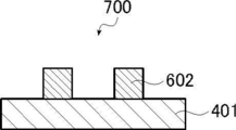
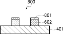
- step B of irradiating light in a pattern to the layer to be plated formation From the step B of irradiating light in a pattern to the layer to be plated formation, the step C of removing the temporary protective film on the layer to be plated formation, and the light in the layer to be plated formation And D) removing the non-irradiated area to form a pattern-like plated layer on the substrate.
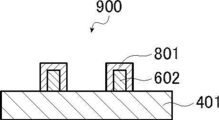
- 4 to 7 are sectional views showing an example of the above embodiment in the order of steps. Each process will be described in detail with reference to the above drawings.
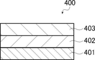
- Process A is a process of producing a laminate including a substrate, a layer for forming a layer to be plated, and a temporary protective film in this order. More specifically, as shown in FIG. 4, in this step, the substrate 401, the layer for plating layer formation 402 disposed on the substrate 401, and the temporary layer on the plating layer formation 402 are disposed. A laminate 400 including the protective film 403 is manufactured. The laminated body 400 obtained by this process corresponds to the laminated body provided with the layer 402 for to-be-plated layer to which the following light irradiation is given.
- each member and each material which were demonstrated as a member and material which comprise the laminated body which is said 1st embodiment can be used suitably for this process.
- this process can use suitably the manufacturing method demonstrated as a manufacturing method of the laminated body which is said 1st embodiment.
- Step B Step of Irradiating Light in Pattern Form to the Layer to be Deposited Layer Formation from the Temporary Protective Film Side in the Laminate (Irradiation Step)]
- This step is a step of irradiating light in a pattern on the layer for plating layer formation 402 from the side of the temporary protective film 403 of the laminate 400 manufactured in the above step (step of exposing in a pattern). That is, this step is a step of irradiating the layer to be plated 402 with light of a wavelength to which the polymerization initiator is sensitive in a pattern.
- region (unexposed part) of the layer for to-be-plated layer formation is removed, and a pattern-form to-be-plated layer is formed.
- the light, rather than the absorption edge lambda 0 of the long wavelength side of the ultraviolet-visible absorption spectrum of the temporary protective layer comprises a wavelength on the long wavelength side
- the polymerization initiator corresponds to light having a wavelength which is sensitive. More specifically, first, as shown in FIG. 5, with respect to a predetermined irradiation area 502 (area to which light is irradiated) of the layer to be plated formation 402, polymerization is performed through the opening of the photomask 501.
- the light of the wavelength to which an initiator is exposed is irradiated.
- the absorption edge on the long wavelength side of the ultraviolet-visible absorption spectrum of each member satisfies the relationship represented by the above-mentioned formula (Z).
- the light irradiated in a pattern from the side of the temporary protective film 403 passes through the temporary protective film 403, and sensitizes the polymerization initiator contained in the layer for plating layer formation 402. Then, a part of the irradiated light passes through the layer to be plated formation 402 and reaches the substrate 401.
- the plated layer forming layer The light transmitted through 402 is absorbed by the substrate 401. Accordingly, it is possible to prevent the light transmitted through the layer to be plated formation 402 from being scattered at the interface of the substrate 401 and entering the layer to be plated formation 402 again. As a result, a desired irradiation region 502 can be formed in the layer for plating layer formation 402.
- FIG. 1 Absorption edge lambda 2 on the long wavelength side of the ultraviolet-visible absorption spectrum of the substrate 401, because than the absorption edge lambda 1 of the long wavelength side of the ultraviolet-visible absorption spectrum of the polymerization initiator in the long wavelength side, the plated layer forming layer The light transmitted through 402 is absorbed by the substrate 401. Accordingly, it is possible to prevent the light transmitted through the layer to be plated formation 402 from being scattered at the interface of the substrate 401 and entering the layer to be plated formation 402 again. As a result, a desired irradiation region 502 can be formed in the layer for plat
- the method for producing a substrate with a pattern-like layer to be plated according to this embodiment is projection exposure Can also be applied.
- the light-irradiated region (irradiated region 502) of the layer 402 for forming a layer to be plated the polymerization between the polymerizable groups and / or the reaction between the substrate and the polymerizable group proceed and the like, thereby curing and becoming insoluble It becomes. This insoluble part becomes what is called a to-be-plated layer.
- the temporary protective film 403 is removed.
- the light irradiated to the layer for to-be-plated layer formation 402 at this process is light of the wavelength to which the polymerization initiator in the layer for to-be-plated layer formation 402 sensitizes. More specifically, the light of wavelength on the short wavelength side than the absorption edge lambda 1 of the long wavelength side of the ultraviolet-visible absorption spectrum of the polymerization initiator.
- the light of the wavelength to which a polymerization initiator is sensitized should just be included, and the light of other wavelengths is included. It is also good.
- the light irradiated to the layer to be plated layer formation 402 may contain light of a wavelength to which the polymerization initiator is sensitive, and the absorption on the long wavelength side of the UV-visible absorption spectrum of the polymerization initiator Light of a wavelength on the longer wavelength side than the end ⁇ 1 may be included.
- the light to be irradiated may be monochromatic light or continuous light as long as the above requirements are satisfied.
- the light source used for irradiating light is not particularly limited as long as the light having the above wavelength can be irradiated, and examples thereof include a mercury lamp, a metal halide lamp, a xenon lamp, a chemical lamp, and a carbon arc lamp.
- the light irradiation time (hereinafter also referred to as “exposure time”) varies depending on the reactivity of the polymerization initiator and / or the light source, but is usually between 10 seconds and 5 hours.
- the energy of light to be irradiated (hereinafter also referred to as “exposure energy”) may be about 10 to 8000 mJ, preferably in the range of 50 to 3000 mJ.
- exposure energy may be about 10 to 8000 mJ, preferably in the range of 50 to 3000 mJ.
- the method in particular of irradiating light in pattern shape is not restrict
- Step C Step of removing the temporary protective film on the layer to be plated formation
- This process is a process of removing the temporary protective film 403 from the layer 402 for to-be-plated layer formation of the laminated body by which exposure was performed to pattern shape at the said process.
- the method for removal is not particularly limited, and known methods can be used. For example, the method of peeling the laminated temporary protective film 403 is mentioned.
- Step D Step of Forming a Patterned Plated Layer on a Substrate by Removing a Region in the Layer to be Plated-Forming Layer which is not irradiated with light
- This process is a process of removing the non-irradiated area 601 (unexposed area) of the layer for plating layer formation 402 to which the above-mentioned irradiation process has been applied.
- the non-irradiated area 601 in the layer to be plated 402 is removed, and the pattern-like layer to be plated 602 is formed. More specifically, as shown in FIGS.
- the non-irradiated region 601 is removed by performing the main treatment on the laminate 600 from which the temporary protective film 403 has been removed by irradiation with light, and a pattern-like object is formed.
- a patterned substrate with a plated layer 700 including the plated layer 602 is obtained.
- the removing method is not particularly limited, and an optimal method is selected according to the compound contained in the layer to be plated layer formation 402, but a solvent in which the compound is dissolved is generally used as the layer to be plated layer forming 402 The method of making it contact is mentioned. More specifically, there is a method using an alkaline solution as a developer.
- the immersion method When removing the non-irradiated area 601 using an alkaline solution, a method (immersing method) of immersing the laminated body 600 subjected to the irradiation step and from which the temporary protective film 403 has been removed in an alkaline solution, and the plating
- coating an alkaline solution on the layer formation layer 402, etc. are mentioned, the immersion method is preferable.
- the immersion time is preferably about 1 to 30 minutes from the viewpoint of productivity and workability.
- a substrate 700 with a pattern-like layer to be plated including the substrate 401 and the pattern-like layer to be plated 602 can be obtained.
- the patterned substrate with a layer to be plated 700 can be used for forming metal films (conductive films). That is, a metal layer can be formed on a pattern-like to-be-plated layer by giving a plating catalyst or its precursor to a pattern-like to-be-plated layer, and giving a plating process further. That is, the pattern of the metal layer can be controlled by controlling the shape of the pattern-like layer to be plated. Moreover, the adhesiveness with respect to the board
- a plating catalyst or a precursor thereof is applied to the pattern-like plated layer of the substrate with a pattern-like layer to be plated, and a pattern-like substrate to which a plating catalyst or its precursor is applied It includes a step of performing a plating process on the plating layer to form a metal layer on the pattern-like layer to be plated (hereinafter, also referred to as a “metal layer forming step”).
- each above-mentioned member, each material, and a manufacturing method can be used suitably.
- the procedure of a metal layer formation process is demonstrated.
- Method layer forming process In this step, a plating catalyst or a precursor thereof is applied to the pattern-like plating layer in the substrate with a pattern-like layer to be plated, and the plating treatment on the pattern-like layer to which the plating catalyst or precursor thereof is applied To form a metal layer on the patterned plating layer. More specifically, by performing this step, as shown in FIG. 8, the metal layer 801 is formed on the pattern-like layer to be plated 602, and a metal layer-containing laminate 800 is obtained.
- step X of applying a plating catalyst or a precursor thereof to the pattern-like layer to be plated and a step of plating the pattern-like layer to which a plating catalyst or a precursor thereof is applied It divides and explains to Y).
- a plating catalyst or a precursor thereof is applied to the patterned plating layer.
- the interactive group derived from the above-mentioned compound adsorbs the added plating catalyst or its precursor depending on the function. More specifically, a plating catalyst or a precursor thereof is applied in the patterned plating layer and on the surface of the patterned plating layer.
- the plating catalyst or its precursor functions as a catalyst and an electrode of the plating process. Therefore, the type of plating catalyst or precursor thereof to be used is appropriately determined according to the type of plating treatment.
- the plating catalyst or precursor thereof to be used is preferably an electroless plating catalyst or a precursor thereof.
- the electroless plating catalyst or the precursor thereof will be described in detail.
- the electroless plating catalyst used in this step is not particularly limited as long as it becomes an active nucleus at the time of electroless plating, and specifically, a metal containing a catalytic ability of an autocatalytic reduction reaction (proportionate to ionization than Ni Of metals known as low electroless plating metals) and the like. Specific examples thereof include Pd, Ag, Cu, Ni, Pt, Au, and Co. Among them, Ag, Pd, Pt or Cu is preferable from the viewpoint of high catalytic ability. A metal colloid may be used as the electroless plating catalyst.
- the electroless plating catalyst precursor used in this step can be used without particular limitation as long as it can be an electroless plating catalyst by a chemical reaction.
- the metal ions of the metals listed above as the electroless plating catalyst are mainly used.
- the metal ion which is an electroless plating catalyst precursor becomes a zerovalent metal which is an electroless plating catalyst by a reduction reaction.
- metal ions that are electroless plating catalyst precursors may be separately converted to a zero-valent metal by a reduction reaction before being immersed in the electroless plating bath to be used as an electroless plating catalyst .
- the precursor of the electroless plating catalyst may be immersed in the electroless plating bath as it is, and may be changed to a metal (electroless plating catalyst) by the reducing agent in the electroless plating bath.
- the metal ion which is an electroless-plating catalyst precursor is provided to a pattern-like to-be-plated layer using a metal salt.
- the metal salt to be used is not particularly limited as long as it is dissolved in an appropriate solvent and dissociated into a metal ion and a base (anion), and M (NO 3 ) n , MCl n , M 2 / n (SO 4 ), M 3 / n (PO 4 ) (M represents an n-valent metal atom), and the like.
- a metal ion what the said metal salt dissociated can be used suitably.
- Ag ion, Cu ion, Ni ion, Co ion, Pt ion, and Pd ion can be mentioned.
- those capable of multidentate coordination are preferable, and in particular, Ag ions, Pd ions, or Cu ions are more preferable in terms of the number of types of functional groups capable of coordination and the catalytic ability.
- a zero-valent metal can also be used as a catalyst used for direct electroplating without electroless plating.
- a solution in which a plating catalyst or a precursor thereof is dispersed or dissolved in a suitable solvent a plating catalyst or a precursor thereof and a solvent
- the solution for applying a catalyst may be prepared, and the solution may be applied onto the pattern-like layer to be plated, or the laminate having the pattern-like layer to be plated may be dipped in the solution.
- Water and / or organic solvents are suitably used as the above-mentioned solvent.
- the organic solvent a solvent which penetrates the pattern-like plated layer is preferable.
- acetone methyl acetoacetate, ethyl acetoacetate, ethylene glycol diacetate, cyclohexanone, acetylacetone, acetophenone, 2- (1-cyclohexenyl) cyclohexanone, Propylene glycol diacetate, triacetin, diethylene glycol diacetate, dioxane, N-methyl pyrrolidone, dimethyl carbonate, or dimethyl cellosolve can be used.
- the pH of the catalyst application solution containing the plating catalyst or its precursor and the solvent is not particularly limited, but the pH is preferably 3.0 or more in that a desired amount of metal layer is likely to be formed at a desired position during plating. It is preferably 7.0, more preferably 3.2 to 6.8, and still more preferably 3.5 to 6.6.
- the method for preparing the catalyst application liquid is not particularly limited, and a predetermined metal salt may be dissolved in an appropriate solvent, and the pH may be adjusted to a predetermined range using an acid or an alkali, as necessary.
- the concentration of the plating catalyst or its precursor in the solution is not particularly limited, but is preferably 0.001 to 50% by mass, and more preferably 0.005 to 30% by mass.
- the time for which the layer to be plated is in contact with the plating catalyst or its precursor (hereinafter also referred to as "contact time") is preferably about 30 seconds to 24 hours, and preferably about 1 minute to 1 hour It is more preferable that
- the adsorption amount of the plating catalyst of the pattern-like layer to be plated or its precursor varies depending on the type of plating bath used, catalyst metal species, interaction type of pattern-like layer to be plated, and the method of use, etc. From the viewpoint of precipitation property, 5 to 1000 mg / m 2 is preferable, 10 to 800 mg / m 2 is more preferable, and 20 to 600 mg / m 2 is still more preferable.
- the method of plating treatment is not particularly limited, and examples thereof include electroless plating treatment and electrolytic plating treatment (electroplating treatment).
- the electroless plating treatment may be performed alone, or after the electroless plating treatment is performed, the electrolytic plating treatment may be further performed.
- so-called silver mirror reaction is included as a type of the above-mentioned electroless plating process.
- a metal ion deposited may be reduced by a silver mirror reaction or the like to form a desired patterned metal layer, and electrolytic plating may be performed thereafter.
- electrolytic plating may be performed thereafter.
- the electroless plating process refers to an operation of depositing a metal by a chemical reaction using a solution in which metal ions to be deposited as plating are dissolved.
- the electroless plating in this step is carried out, for example, by washing the laminate provided with the pattern-like plated layer to which the electroless plating catalyst has been applied, to remove excess electroless plating catalyst (metal), and then the electroless plating bath. It is preferable to carry out by immersing in As the electroless plating bath to be used, a known electroless plating bath can be used.
- an electroless plating bath in a state where the electroless plating catalyst precursor is adsorbed or impregnated into the pattern-like plated layer.
- the laminate is washed with water to remove excess electroless plating catalyst precursor (such as a metal salt), and then immersed in an electroless plating bath.
- electroless plating catalyst precursor such as a metal salt
- reduction of the electroless plating catalyst precursor and subsequent electroless plating are performed in the electroless plating bath.
- a well-known electroless-plating bath can be used similarly to the above.
- the reduction of the electroless plating catalyst precursor may be performed separately from the above-described embodiment using the electroless plating solution by preparing a catalyst activation solution (reduction solution) and performing it as a separate step before the electroless plating. It is possible.
- composition of a general electroless plating bath in addition to a solvent (for example, water), Metal ions for plating; Reductant, 3.
- Additives (stabilizers) which improve the stability of metal ions are mainly included.
- the plating bath may contain known additives such as a stabilizer for the plating bath.
- the organic solvent used in the electroless plating bath needs to be a solvent that can be used in water, and from this point, ketones such as acetone, and alcohols such as methanol, ethanol, and isopropanol are preferable.
- the immersion time in the electroless plating bath is preferably about 1 minute to 6 hours, and more preferably about 1 minute to 3 hours.
- the catalyst or the pattern-like plating layer to which the precursor is applied is electrically Plating can be performed.
- electrolytic plating can be performed after the above-described electroless plating, if necessary.
- the thickness of the metal layer to be formed can be appropriately adjusted.
- a conventionally known method can be used as the method of electroplating.
- copper, chromium, lead, nickel, gold, silver, tin, zinc etc. are mentioned, From a conductive viewpoint, copper, gold, or silver is preferable, and copper is more preferable. preferable.
- a metal layer (plating layer) can be formed on the pattern-like layer to be plated.
- the subtractive method is used to form the metal layer, there is a to-be-plated layer made of a hydrophilic resin or the like between the patterned metal layers, so when the pattern of the metal layer is further refined Migration of metal ions is likely to occur due to the influence of the layer to be plated, and there is a concern that the insulating property may be reduced (the formation of a metal layer by the subtractive method is described in JP 2012-097296, etc.).
- the above procedure of the present invention is a so-called additive method of forming a pattern-like plating layer and forming a metal layer corresponding to the conductive layer on the pattern-like layer, and a metal layer obtained by this method Since the to-be-plated layer does not remain between the metal layers in the containing laminate, the occurrence of migration is further suppressed, and can be suitably used as a conductive film for a touch panel sensor.
- the metal layer 801 is arrange
- It may be a metal layer-containing laminate (900) in which the metal layer 801 is disposed on the surface of the layer 602 other than the contact surface with the substrate 401. That is, the metal layer may be disposed to cover the surface of the pattern-like layer to be plated other than the contact surface with the substrate.
- the pattern-like to-be-plated layer was arrange
- the metal layer-containing laminate obtained by the above processing can be applied to various applications, and can be applied to touch panels (or touch panel sensors), semiconductor chips, various electric wiring boards, flexible printed circuits (FPCs), chip on films (COFs)
- the present invention can be applied to various applications such as TAB (Tape Automated Bonding), antennas, multilayer wiring boards, and motherboards.
- a touch panel sensor electronic capacitance type touch panel sensor.
- the metal layer in a metal layer containing laminated body functions as a detection electrode or lead-out wiring in a touch panel sensor.
- a touch panel sensor a combination of a touch panel sensor and various display devices (for example, a liquid crystal display device or an organic EL (electro-luminescence) display device) is called a touch panel.
- a touch panel a so-called capacitive touch panel is preferably mentioned.
- Substrate S1-2 The substrate formed into a film by the same method as the above S1-1 was S1-2 except that F5023 (Arton film manufactured by JSR Corporation) was dissolved in toluene and the ultraviolet absorber 1 was added so as to be 2% by mass in the resin component. .
- F5023 Article film manufactured by JSR Corporation
- composition for forming primer layer A solution of 100 g of hydrogenated nitrile butadiene rubber Zetpole 0020 (manufactured by Nippon Zeon Co., Ltd.) dissolved in 900 g of cyclopentanone (manufactured by Tokyo Chemical Industry Co., Ltd.) was used as a composition for forming a primer layer.
- composition for forming a layer to be plated [Preparation of composition for forming a layer to be plated] ⁇ Preparation of composition for formation of the layer for to-be-plated layer formation (Hereinafter, it is only called "the composition for to-be-plated layer formation.”1)> 2-propanol 96.85 mass% 0.82 mass% of polyacrylic acid FFM-2 (manufactured by Wako Pure Chemical Industries, Ltd.) 2.18% by mass IRGACURE 127 (manufactured by BASF) 0.15 mass% The composition described above was mixed to obtain a composition 1 for forming a layer to be plated. The structure of FFM-2 is shown in the following formula (A).
- composition 2 for Forming Plated Layer 2-propanol 96.85 mass% 0.82 mass% of polyacrylic acid FFM-2 (manufactured by Wako Pure Chemical Industries, Ltd.) 2.18% by mass IRGACURE OXE 02 (manufactured by BASF) 0.15 mass%
- FFM-2 polyacrylic acid
- IRGACURE OXE 02 manufactured by BASF
- composition 3 for Forming Plated Layer 2-propanol 6.85% by mass 0.82 mass% of polyacrylic acid FFM-2 (manufactured by Wako Pure Chemical Industries, Ltd.) 2.18% by mass IRGACURE 819 (manufactured by BASF) 0.075% by mass IRGACURE 184 (manufactured by BASF) 0.075% by mass
- the above composition was mixed to obtain a composition 3 for forming a layer to be plated.
- composition 4 for Forming Plated Layer 2-propanol 96.85 mass% Polymer 1 3 mass% IRGACURE OXE 02 (manufactured by BASF) 0.15 mass%
- the composition described above was mixed to obtain a composition 4 for forming a layer to be plated.
- the structure of polymer 1 is shown below.
- the polymer 1 was synthesized by the following method. In a 2 L three-necked flask, 1 L of ethyl acetate and 159 g of 2-aminoethanol were charged, and cooled in an ice bath. Thereto, 150 g of 2-bromoisobutyric acid bromide was added dropwise while adjusting to an internal temperature of 20 ° C. or less. Thereafter, the internal temperature was raised to room temperature (25.degree. C.) and allowed to react for 2 hours. After completion of the reaction, 300 mL of distilled water was added to the reaction solution to stop the reaction.
- the ethyl acetate phase was washed four times with 300 mL of distilled water and then dried over magnesium sulfate, and then ethyl acetate was distilled off to obtain 80 g of a raw material A.
- 47.4 g of the raw material A, 22 g of pyridine, and 150 mL of ethyl acetate were placed in a 500 mL three-necked flask, and cooled in an ice bath. Thereto, 25 g of acrylic acid chloride was adjusted to an internal temperature of 20 ° C. or less and dropped. Thereafter, the internal temperature was raised to room temperature and reacted for 3 hours.
- the identification of the obtained polymer 1 was performed using IR (Infrared radiation) measuring machine (made by Horiba, Ltd.). The measurement was carried out by dissolving the polymer in acetone and using KBr crystals. As a result of IR measurement, a peak was observed around 2240 cm -1 , and it was found that acrylonitrile, which is a nitrile unit, was introduced into the polymer. Moreover, it turned out that acrylic acid is introduce
- DMSO dimethyl sulfoxide
- the peak corresponding to the nitrile unit is observed broad at 2.5 to 0.7 ppm (5H), and the peak corresponding to the polymerizable group unit is 7.8 to 8.1 ppm (1H), 5.8-5 .6 ppm (1 H), 5.4-5.2 ppm (1 H), 4.2-3.9 ppm (2 H), 3.3-3.5 ppm (2 H), 2.5-0.7 ppm
- Example 1 A composition for forming a primer layer was applied by a bar coater on the surface on one side of the substrate S1-3 so that the thickness after drying was 1 ⁇ m, to prepare a coated film. The coating was dried in an oven at 140 ° C. for 10 minutes to form a primer layer on the surface of one side of the substrate. Then, the composition 1 for to-be-plated layer forming was apply
- F5023 100 micrometers in thickness
- F5023 100 micrometers in thickness
- a temporary protective film is adhered to a photomask that can simultaneously form both a 150 ⁇ m square grid pattern with a 2 ⁇ m wiring width and a pattern in which multiple straight lines of 1 mm wiring width are arranged in parallel at 2 mm intervals. It exposed so that exposure energy might be 4500 mJ using the ultraviolet ray lamp Deep UV Lamp (made by Ushio company) which can radiate
- the ultraviolet ray lamp Deep UV Lamp made by Ushio company
- the temporary protective film is peeled from the laminate, and the laminate from which the temporary protective film has been removed is developed by being immersed in a 1 mass% sodium carbonate aqueous solution heated to 40 ° C. for 5 minutes, I got the substrate.
- This substrate with a pattern-like layer to be plated is immersed for 5 minutes at room temperature in a solution obtained by diluting only MAT-2A of Pd catalyst application liquid MAT-2 (made by Kamimura Kogyo Co., Ltd.) 5 times and pulled up, then pure water And washed twice.
- the substrate with the patterned layer to be plated after the cleaning was immersed in a reducing agent MAB (manufactured by Kamimura Kogyo Co., Ltd.) for 5 minutes at 36 ° C., pulled up, and then washed twice with pure water. Thereafter, the substrate with the pattern-like layer to be plated after the cleaning is immersed for 60 minutes at room temperature in electroless plating solution Sul cup PEA (made by Kamimura Kogyo Co., Ltd.) for 60 minutes, pulled up, washed with pure water, and containing metal layer A laminate was obtained.
- the said metal layer can be used as wiring for touch panels.
- Example 2 Example except that the substrate was changed to S1-1, the composition 1 for forming a layer to be plated was changed to the composition 2 for forming a layer to be plated, the temporary protective film was changed to ZF 14 (thickness 100 ⁇ m), and the exposure amount was changed to 300 mJ. In the same manner as in No. 1, a metal layer-containing laminate was produced.
- Example 3 The substrate was changed to S1-1, the composition 1 for forming a layer to be plated was changed to the composition 2 for forming a layer to be plated, and the temporary protective film was changed to 16QS62 (PET film manufactured by Toray Industries, 16 ⁇ m thick), and the exposure dose was 300 mJ.
- a metal layer-containing laminate was produced in the same manner as in Example 1 except for the change.
- Example 4 A metal layer-containing laminate was prepared in the same manner as in Example 1 except that the substrate was changed to S1-2, the composition 1 for forming a layer to be plated was changed to the composition 2 for forming a layer to be plated, and the exposure dose was changed to 300 mJ Made.
- Example 5 The substrate was changed to S1-2, the composition 1 for forming a layer to be plated was changed to the composition 2 for forming a layer to be plated, and the temporary protective film was changed to 16QS62 (PET film manufactured by Toray Industries, 16 ⁇ m thick), and the exposure amount was 300 mJ.
- a metal layer-containing laminate was produced in the same manner as in Example 1 except for the change.
- Example 6 A metal layer-containing laminate was prepared in the same manner as in Example 1 except that the substrate was changed to S1-4, the composition 1 for forming a layer to be plated was changed to the composition 2 for forming a layer to be plated, and the exposure dose was changed to 300 mJ Made.
- Example 7 The substrate was changed to S1-4, the composition 1 for forming a layer to be plated was changed to the composition 2 for forming a layer to be plated, and the temporary protective film was changed to 16QS62 (PET film manufactured by Toray Industries, 16 ⁇ m thick), and the exposure was 300 mJ A metal layer-containing laminate was produced in the same manner as in Example 1 except for the change.
- Example 8 Change the substrate to S1-4, the composition to form a layer to be plated 1 to the composition to form a layer to be plated 4 and the temporary protective film to 16QS 62 (PET film manufactured by Toray Industries, 16 ⁇ m) and change the exposure amount to 300 mJ A metal layer-containing laminate was produced in the same manner as in Example 1 except for the above.
- Comparative Example 1 Except that the substrate was changed to ZF 14 (thickness 100 ⁇ m), the composition 1 for forming a layer to be plated was changed to composition 2 for forming a layer to be plated, the temporary protective film was changed to ZF 14 (thickness 100 ⁇ m), and the exposure was changed to 300 mJ A metal layer-containing laminate was produced in the same manner as in Example 1.
- Comparative Example 2 Metal layer-containing lamination in the same manner as in Example 1 except that the substrate was changed to F5023 (thickness 100 ⁇ m), composition 1 for forming a layer to be plated was changed to composition 2 for forming a layer to be plated, and the exposure amount was changed to 300 mJ. The body was made.
- Comparative Example 3 A metal layer-containing laminate was produced in the same manner as in Example 1 except that the composition 1 for forming a layer to be plated was changed to the composition 2 for forming a layer to be plated and the exposure dose was changed to 300 mJ.
- Comparative Example 4 Example 1 except that the composition 1 for forming a layer to be plated was changed to the composition 2 for forming a layer to be plated, the temporary protective film was changed to 16QS 62 (PET film manufactured by Toray Industries, thickness 16 ⁇ m), and the exposure amount was changed to 300 mJ.
- a metal layer-containing laminate was produced in the same manner as in the above.
- Comparative Example 5 Example except that the substrate was changed to S1-1, the composition 1 for forming a layer to be plated was changed to the composition 3 for forming a layer to be plated, the temporary protective film was changed to ZF 14 (thickness 100 ⁇ m), and the exposure amount was changed to 3000 mJ. A metal layer-containing laminate was produced in the same manner as 1).
- Comparative Example 6 The substrate was changed to S1-1, the composition 1 for forming a layer to be plated was changed to the composition 3 for forming a layer to be plated, the temporary protective film was changed to 16QS62 (PET film manufactured by Toray Industries, Inc. 16 ⁇ m), and the exposure was changed to 3000 mJ.
- a metal layer-containing laminate was produced in the same manner as in Example 1 except for the above.
- Comparative Example 7 The metal layer-containing laminate was prepared in the same manner as in Example 1 except that the substrate was changed to S1-2, the composition 1 for forming a layer to be plated was changed to the composition 3 for forming a layer to be plated, and the exposure dose was changed to 3000 mJ. Made.
- Comparative Example 8 The substrate was changed to S1-2, the composition 1 for forming a layer to be plated was changed to the composition 3 for forming a layer to be plated, the temporary protective film was changed to 16QS 62 (PET film manufactured by Toray Industries, 16 ⁇ m), and the exposure was changed to 300 mJ.
- a metal layer-containing laminate was produced in the same manner as in Example 1 except for the above.
- Comparative Example 9 A metal layer-containing laminate was prepared in the same manner as in Example 1 except that the substrate was changed to S1-4, the composition 1 for forming a layer to be plated was changed to the composition 3 for forming a layer to be plated, and the exposure dose was changed to 3000 mJ. Made.
- Comparative Example 10 Change the substrate to S1-4, the composition to form a layer to be plated 1 to the composition to form a layer to be plated 3, the temporary protective film to 16QS 62 (PET film manufactured by Toray Industries, 16 ⁇ m) and change the exposure amount to 3000 mJ
- a metal layer-containing laminate was produced in the same manner as in Example 1 except for the above.
- the absorption edge ⁇ 0 on the long wavelength side of the UV-visible absorption spectrum of the temporary protective film of each of the Examples and Comparative Examples, the absorption edge ⁇ 1 on the long wavelength side of the UV-visible absorption spectrum of the polymerization initiator, and the substrate position of the absorption edge lambda 2 on the long wavelength side of the ultraviolet-visible absorption spectrum (nm) are summarized in Table 1. The method of determining this absorption end is as described above.
Landscapes
- Chemical & Material Sciences (AREA)
- Physics & Mathematics (AREA)
- Chemical Kinetics & Catalysis (AREA)
- Engineering & Computer Science (AREA)
- Polymers & Plastics (AREA)
- Medicinal Chemistry (AREA)
- Organic Chemistry (AREA)
- Health & Medical Sciences (AREA)
- General Physics & Mathematics (AREA)
- Spectroscopy & Molecular Physics (AREA)
- Manufacturing & Machinery (AREA)
- Architecture (AREA)
- Structural Engineering (AREA)
- Inorganic Chemistry (AREA)
- Materials Engineering (AREA)
- General Engineering & Computer Science (AREA)
- Theoretical Computer Science (AREA)
- Ceramic Engineering (AREA)
- Human Computer Interaction (AREA)
- Laminated Bodies (AREA)
- Materials For Photolithography (AREA)
- Manufacturing Of Printed Wiring (AREA)
Abstract
Priority Applications (4)
| Application Number | Priority Date | Filing Date | Title |
|---|---|---|---|
| KR1020187026732A KR102111875B1 (ko) | 2016-03-23 | 2017-02-14 | 적층체, 패턴 형상 피도금층이 있는 기판의 제조 방법, 금속층 함유 적층체의 제조 방법, 터치 패널 센서, 및 터치 패널 |
| CN201780018149.4A CN108778724B (zh) | 2016-03-23 | 2017-02-14 | 层叠体、带图案状被镀层的基板的制造方法、含有金属层的层叠体的制造方法、触摸面板传感器及触摸面板 |
| JP2018507124A JP6612970B2 (ja) | 2016-03-23 | 2017-02-14 | 積層体、パターン状被めっき層付き基板の製造方法、金属層含有積層体の製造方法、タッチパネルセンサー、及びタッチパネル |
| US16/132,503 US10766233B2 (en) | 2016-03-23 | 2018-09-17 | Laminate, method for producing substrate with patterned plated layer, method for producing metal layer-containing laminate, touch panel sensor, and touch panel |
Applications Claiming Priority (2)
| Application Number | Priority Date | Filing Date | Title |
|---|---|---|---|
| JP2016-059242 | 2016-03-23 | ||
| JP2016059242 | 2016-03-23 |
Related Child Applications (1)
| Application Number | Title | Priority Date | Filing Date |
|---|---|---|---|
| US16/132,503 Continuation US10766233B2 (en) | 2016-03-23 | 2018-09-17 | Laminate, method for producing substrate with patterned plated layer, method for producing metal layer-containing laminate, touch panel sensor, and touch panel |
Publications (1)
| Publication Number | Publication Date |
|---|---|
| WO2017163669A1 true WO2017163669A1 (fr) | 2017-09-28 |
Family
ID=59899973
Family Applications (1)
| Application Number | Title | Priority Date | Filing Date |
|---|---|---|---|
| PCT/JP2017/005269 Ceased WO2017163669A1 (fr) | 2016-03-23 | 2017-02-14 | Corps stratifié, procédé de production d'un substrat doté d'une couche plaquée à motifs, procédé de production d'un corps stratifié contenant une couche métallique, et capteur de panneau tactile ainsi que panneau tactile |
Country Status (6)
| Country | Link |
|---|---|
| US (1) | US10766233B2 (fr) |
| JP (1) | JP6612970B2 (fr) |
| KR (1) | KR102111875B1 (fr) |
| CN (1) | CN108778724B (fr) |
| TW (1) | TWI712490B (fr) |
| WO (1) | WO2017163669A1 (fr) |
Families Citing this family (2)
| Publication number | Priority date | Publication date | Assignee | Title |
|---|---|---|---|---|
| KR102112435B1 (ko) * | 2016-03-23 | 2020-05-18 | 후지필름 가부시키가이샤 | 도전성 적층체의 제조 방법과, 피도금층 전구체층을 구비한 입체 구조물, 패턴 형상 피도금층을 구비한 입체 구조물, 도전성 적층체, 터치 센서, 발열 부재 및 입체 구조물 |
| KR102283020B1 (ko) * | 2019-01-28 | 2021-07-28 | 동우 화인켐 주식회사 | 터치 센서 적층체 및 화상 표시 장치 |
Citations (3)
| Publication number | Priority date | Publication date | Assignee | Title |
|---|---|---|---|---|
| JP2010248464A (ja) * | 2008-09-26 | 2010-11-04 | Fujifilm Corp | 被めっき層形成用組成物、金属パターン材料の作製方法、及び、新規ポリマー |
| JP2011186208A (ja) * | 2010-03-09 | 2011-09-22 | Asahi Kasei E-Materials Corp | 感光性樹脂組成物 |
| JP2012194534A (ja) * | 2011-02-28 | 2012-10-11 | Fujifilm Corp | 感光性組成物、感光性ソルダーレジスト組成物及び感光性ソルダーレジストフィルム、並びに、永久パターン、その形成方法及びプリント基板 |
Family Cites Families (8)
| Publication number | Priority date | Publication date | Assignee | Title |
|---|---|---|---|---|
| JP4684632B2 (ja) | 2003-11-27 | 2011-05-18 | 富士フイルム株式会社 | 金属パターン形成方法、金属パターン及びプリント配線板 |
| JP5164502B2 (ja) | 2006-10-23 | 2013-03-21 | 富士フイルム株式会社 | ニトリル基含有ポリマー、その合成方法、ニトリル基含有ポリマーを用いた組成物、及び積層体 |
| JP5448524B2 (ja) | 2008-04-23 | 2014-03-19 | 富士フイルム株式会社 | めっき用積層フィルム、表面金属膜材料の作製方法及び表面金属膜材料 |
| JP5258489B2 (ja) | 2008-09-30 | 2013-08-07 | 富士フイルム株式会社 | 金属膜形成方法 |
| JP2011094192A (ja) * | 2009-10-29 | 2011-05-12 | Fujifilm Corp | 被めっき層形成用組成物、金属パターン材料の作製方法、及び金属パターン材料 |
| JP5661533B2 (ja) * | 2010-05-28 | 2015-01-28 | 富士フイルム株式会社 | 導電シートの製造方法及びタッチパネルの製造方法 |
| JP2012097296A (ja) | 2010-10-29 | 2012-05-24 | Fujifilm Corp | 金属膜形成方法 |
| EP2666629A4 (fr) * | 2011-01-20 | 2014-09-17 | Asahi Glass Co Ltd | Substrat en résine pourvu de revêtement de couche dure et son procédé de fabrication |
-
2017
- 2017-02-14 JP JP2018507124A patent/JP6612970B2/ja active Active
- 2017-02-14 WO PCT/JP2017/005269 patent/WO2017163669A1/fr not_active Ceased
- 2017-02-14 CN CN201780018149.4A patent/CN108778724B/zh active Active
- 2017-02-14 KR KR1020187026732A patent/KR102111875B1/ko not_active Expired - Fee Related
- 2017-03-09 TW TW106107668A patent/TWI712490B/zh active
-
2018
- 2018-09-17 US US16/132,503 patent/US10766233B2/en active Active
Patent Citations (3)
| Publication number | Priority date | Publication date | Assignee | Title |
|---|---|---|---|---|
| JP2010248464A (ja) * | 2008-09-26 | 2010-11-04 | Fujifilm Corp | 被めっき層形成用組成物、金属パターン材料の作製方法、及び、新規ポリマー |
| JP2011186208A (ja) * | 2010-03-09 | 2011-09-22 | Asahi Kasei E-Materials Corp | 感光性樹脂組成物 |
| JP2012194534A (ja) * | 2011-02-28 | 2012-10-11 | Fujifilm Corp | 感光性組成物、感光性ソルダーレジスト組成物及び感光性ソルダーレジストフィルム、並びに、永久パターン、その形成方法及びプリント基板 |
Also Published As
| Publication number | Publication date |
|---|---|
| TWI712490B (zh) | 2020-12-11 |
| TW201733795A (zh) | 2017-10-01 |
| KR20180112850A (ko) | 2018-10-12 |
| US10766233B2 (en) | 2020-09-08 |
| CN108778724A (zh) | 2018-11-09 |
| CN108778724B (zh) | 2020-07-03 |
| JP6612970B2 (ja) | 2019-11-27 |
| KR102111875B1 (ko) | 2020-05-15 |
| US20190016101A1 (en) | 2019-01-17 |
| JPWO2017163669A1 (ja) | 2019-01-31 |
Similar Documents
| Publication | Publication Date | Title |
|---|---|---|
| TWI742055B (zh) | 導電性積層體的製造方法以及帶被鍍覆層前驅體層的立體結構物、帶圖案狀被鍍覆層的立體結構物、導電性積層體、觸控感測器及發熱構件 | |
| JP6145219B2 (ja) | タッチパネル用導電性積層体、タッチパネル、透明導電性積層体 | |
| TW201715309A (zh) | 被鍍覆層形成用組合物、帶被鍍覆層前體層的膜、帶圖案狀被鍍覆層的膜、導電性膜、觸控面板 | |
| JPWO2015190484A6 (ja) | タッチパネル用導電性積層体、タッチパネル、透明導電性積層体 | |
| JP6402196B2 (ja) | パターン状被めっき層含有積層体の製造方法、金属層含有積層体の製造方法、タッチパネルセンサー、タッチパネル、パターン状被めっき層含有積層体、金属層含有積層体 | |
| JP6295330B2 (ja) | タッチパネルセンサー用導電性積層体、および、その製造方法、タッチパネルセンサー、タッチパネル | |
| JP6611396B2 (ja) | 被めっき層形成用組成物、被めっき層前駆体層付きフィルム、パターン状被めっき層付きフィルム、導電性フィルム、タッチパネル | |
| JP6275861B2 (ja) | 積層体、導電性積層体およびその製造方法、タッチパネルセンサー、タッチパネル、転写フィルム | |
| JP6612970B2 (ja) | 積層体、パターン状被めっき層付き基板の製造方法、金属層含有積層体の製造方法、タッチパネルセンサー、及びタッチパネル | |
| WO2016009829A1 (fr) | Film conducteur destiné à un capteur d'écran tactile, capteur d'écran tactile, et écran tactile | |
| WO2017170012A1 (fr) | Procédé de production d'un stratifié contenant une ligne de câblage métallique, stratifié contenant une ligne de câblage métallique et substrat doté d'une couche à plaquer |
Legal Events
| Date | Code | Title | Description |
|---|---|---|---|
| WWE | Wipo information: entry into national phase |
Ref document number: 2018507124 Country of ref document: JP |
|
| ENP | Entry into the national phase |
Ref document number: 20187026732 Country of ref document: KR Kind code of ref document: A |
|
| WWE | Wipo information: entry into national phase |
Ref document number: 1020187026732 Country of ref document: KR |
|
| NENP | Non-entry into the national phase |
Ref country code: DE |
|
| 121 | Ep: the epo has been informed by wipo that ep was designated in this application |
Ref document number: 17769716 Country of ref document: EP Kind code of ref document: A1 |
|
| 122 | Ep: pct application non-entry in european phase |
Ref document number: 17769716 Country of ref document: EP Kind code of ref document: A1 |