WO2017163972A1 - Revêtement dur, élément recouvert de revêtement dur et procédé pour la production de revêtement dur - Google Patents
Revêtement dur, élément recouvert de revêtement dur et procédé pour la production de revêtement dur Download PDFInfo
- Publication number
- WO2017163972A1 WO2017163972A1 PCT/JP2017/009922 JP2017009922W WO2017163972A1 WO 2017163972 A1 WO2017163972 A1 WO 2017163972A1 JP 2017009922 W JP2017009922 W JP 2017009922W WO 2017163972 A1 WO2017163972 A1 WO 2017163972A1
- Authority
- WO
- WIPO (PCT)
- Prior art keywords
- hard coating
- film
- hard
- atomic ratio
- less
- Prior art date
- Legal status (The legal status is an assumption and is not a legal conclusion. Google has not performed a legal analysis and makes no representation as to the accuracy of the status listed.)
- Ceased
Links
Images




Classifications
-
- B—PERFORMING OPERATIONS; TRANSPORTING
- B23—MACHINE TOOLS; METAL-WORKING NOT OTHERWISE PROVIDED FOR
- B23B—TURNING; BORING
- B23B27/00—Tools for turning or boring machines; Tools of a similar kind in general; Accessories therefor
- B23B27/14—Cutting tools of which the bits or tips or cutting inserts are of special material
-
- B—PERFORMING OPERATIONS; TRANSPORTING
- B23—MACHINE TOOLS; METAL-WORKING NOT OTHERWISE PROVIDED FOR
- B23B—TURNING; BORING
- B23B51/00—Tools for drilling machines
-
- B—PERFORMING OPERATIONS; TRANSPORTING
- B23—MACHINE TOOLS; METAL-WORKING NOT OTHERWISE PROVIDED FOR
- B23C—MILLING
- B23C5/00—Milling-cutters
- B23C5/16—Milling-cutters characterised by physical features other than shape
-
- B—PERFORMING OPERATIONS; TRANSPORTING
- B23—MACHINE TOOLS; METAL-WORKING NOT OTHERWISE PROVIDED FOR
- B23G—THREAD CUTTING; WORKING OF SCREWS, BOLT HEADS, OR NUTS, IN CONJUNCTION THEREWITH
- B23G5/00—Thread-cutting tools; Die-heads
- B23G5/02—Thread-cutting tools; Die-heads without means for adjustment
- B23G5/06—Taps
-
- C—CHEMISTRY; METALLURGY
- C23—COATING METALLIC MATERIAL; COATING MATERIAL WITH METALLIC MATERIAL; CHEMICAL SURFACE TREATMENT; DIFFUSION TREATMENT OF METALLIC MATERIAL; COATING BY VACUUM EVAPORATION, BY SPUTTERING, BY ION IMPLANTATION OR BY CHEMICAL VAPOUR DEPOSITION, IN GENERAL; INHIBITING CORROSION OF METALLIC MATERIAL OR INCRUSTATION IN GENERAL
- C23C—COATING METALLIC MATERIAL; COATING MATERIAL WITH METALLIC MATERIAL; SURFACE TREATMENT OF METALLIC MATERIAL BY DIFFUSION INTO THE SURFACE, BY CHEMICAL CONVERSION OR SUBSTITUTION; COATING BY VACUUM EVAPORATION, BY SPUTTERING, BY ION IMPLANTATION OR BY CHEMICAL VAPOUR DEPOSITION, IN GENERAL
- C23C14/00—Coating by vacuum evaporation, by sputtering or by ion implantation of the coating forming material
- C23C14/06—Coating by vacuum evaporation, by sputtering or by ion implantation of the coating forming material characterised by the coating material
-
- C—CHEMISTRY; METALLURGY
- C23—COATING METALLIC MATERIAL; COATING MATERIAL WITH METALLIC MATERIAL; CHEMICAL SURFACE TREATMENT; DIFFUSION TREATMENT OF METALLIC MATERIAL; COATING BY VACUUM EVAPORATION, BY SPUTTERING, BY ION IMPLANTATION OR BY CHEMICAL VAPOUR DEPOSITION, IN GENERAL; INHIBITING CORROSION OF METALLIC MATERIAL OR INCRUSTATION IN GENERAL
- C23C—COATING METALLIC MATERIAL; COATING MATERIAL WITH METALLIC MATERIAL; SURFACE TREATMENT OF METALLIC MATERIAL BY DIFFUSION INTO THE SURFACE, BY CHEMICAL CONVERSION OR SUBSTITUTION; COATING BY VACUUM EVAPORATION, BY SPUTTERING, BY ION IMPLANTATION OR BY CHEMICAL VAPOUR DEPOSITION, IN GENERAL
- C23C14/00—Coating by vacuum evaporation, by sputtering or by ion implantation of the coating forming material
- C23C14/22—Coating by vacuum evaporation, by sputtering or by ion implantation of the coating forming material characterised by the process of coating
- C23C14/24—Vacuum evaporation
- C23C14/32—Vacuum evaporation by explosion; by evaporation and subsequent ionisation of the vapours, e.g. ion-plating
Definitions
- the present invention relates to a hard coating, a hard coating covering member provided with the hard coating, and a method of manufacturing the hard coating.
- Patent Documents 1 and 2 and Non-Patent Document 1 disclose forming a hard film made of AlCrN on the surface of a base material such as a cutting tool.
- Patent Document 1 and Non-Patent Document 1 listed below disclose an AlCrN film containing 70 at% or more of Al formed on a substrate.
- Patent Document 2 below discloses that an AlCrN film containing Al of less than 70 at% is formed on a substrate.
- the AlCrN film has a metastable cubic crystal structure in which Al is dissolved in the crystal lattice of CrN.
- the state in which Al is dissolved in the crystal lattice of CrN becomes unstable, and hexagonal AlN that is a stable phase is generated. . Since such a hexagonal crystal structure is inferior in mechanical properties, the following patent document 1 and non-patent document 1 cannot obtain a hard film having excellent wear resistance.
- a film having a low Al content as in Patent Document 2 below has a crystal structure in which coarse cubic crystals of AlCrN are generated.
- the Young's modulus is increased while the film is hardened. For this reason, since the deformability with respect to the force from the outside becomes poor, there is a problem that it easily develops into a crack and is inferior in wear resistance.
- An object of the present invention is to provide a hard film with improved wear resistance, a hard film-coated member provided with the hard film, and a method for producing the hard film.
- a hard film according to one aspect of the present invention is a hard film containing Al, Cr, and N, and has a composition formula of Al m Cr 1-m N 1-xyz C x B y O z. Is.
- m represents the atomic ratio of Al to the total of Al and Cr.
- 1-m represents the atomic ratio of Cr to the total of Al and Cr.
- 1-xyz represents the atomic ratio of N to the total of N, C, B, and O.
- x represents the atomic ratio of C to the total of N, C, B, and O.
- y represents the atomic ratio of B to the total of N, C, B, and O.
- z represents the atomic ratio of O to the total of N, C, B, and O.
- the relational expressions 0.68 ⁇ m ⁇ 0.85 and y ⁇ 0.10 are satisfied.
- the hard coating has a cubic rock salt type crystal structure.
- H hardness of the hard film
- E Young's modulus
- the ratio H / E to the Young's modulus is 0.050 or more and 0.120 or less. Yes and H is 20 GPa or more.
- a hard film covering member includes a base material and the hard film formed on the surface of the base material.
- a method for producing a hard coating according to still another aspect of the present invention comprises a composition formula of Al m Cr 1-m N 1-xyZ C x B y O z and has a cubic rock salt type crystal structure. This is a method of forming a hard film having a surface on the surface of a substrate.
- m represents the atomic ratio of Al to the total of Al and Cr.
- 1-m represents the atomic ratio of Cr to the total of Al and Cr.
- 1-xyz represents the atomic ratio of N to the total of N, C, B, and O.
- x represents the atomic ratio of C to the total of N, C, B, and O.
- y represents the atomic ratio of B to the total of N, C, B, and O.
- the hard coating is formed on the surface of the substrate by placing the substrate on a stage, installing a target having a component composition of the hard coating, and evaporating the target. And a film forming step.
- a bias voltage is applied to the substrate so that a bias voltage V applied from the stage to the substrate satisfies a relational expression of ⁇ 316 ⁇ V ⁇ ⁇ 214.3m + 110. Then, the hard film is formed.
- a hard film according to an embodiment of the present invention is a hard film containing Al, Cr, and N, and has a composition formula of Al m Cr 1-m N 1-xyZ C x B y O z. Is. In this composition, the relational expressions of 0.68 ⁇ m ⁇ 0.85 and y ⁇ 0.10 are satisfied.
- This hard film has a cubic rock salt type crystal structure.
- the hardness of the hard film is H (GPa) and the Young's modulus of the hard film is E (GPa)
- the ratio of hardness to Young's modulus is H / E of 0.050 or more and 0.120 or less. Yes and H is 20 GPa or more.
- the H / E is 0.050 or more and 0.120 or less by adjusting the Al content in the range of 0.68 ⁇ m ⁇ 0.85 and adjusting the hardness H and Young's modulus E.
- H is in the range of 20 GPa or more (H ⁇ 20 GPa).
- H / E of less than 0.050
- the Young's modulus E is too high with respect to the hardness H, so that the deformation amount of the film when an external force is applied is reduced. Therefore, since cracking is likely to occur, the wear resistance is reduced.
- H / E is too large (exceeding 0.120)
- the Young's modulus E becomes too low, so that it becomes difficult to fulfill the function as a hard film.
- the hard coating has a cubic rock salt type crystal structure, and by adjusting the H / E to a range of 0.050 to 0.120 in a range where the hardness H is 20 GPa or more, Abrasion resistance has been dramatically improved.
- H / E is preferably 0.0505 or more, more preferably 0.0510 or more, further preferably 0.0515 or more, and further preferably 0.0520 or more.
- H / E is preferably 0.058 or more, more preferably 0.060 or more, and further preferably 0.061 or more.
- H / E is preferably 0.10 or less, and more preferably 0.09 or less.
- the hardness H is preferably 22 GPa or more, more preferably 24 GPa or more, further preferably 25 GPa or more, and further preferably 26 GPa or more.
- Hardness H (GPa)” and “Young's modulus E (GPa)” of the hard coating are measured by performing a nanoindentation test using a cemented carbide test piece on which the hard coating is formed.
- nano indenter “ENT-1100 manufactured by Elionix Co., Ltd.” is used as an apparatus.
- the indenter uses a Belkovic triangular pyramid indenter.
- the atomic ratios of Al, Cr, N, C, B, and O in the hard coating can be measured using an energy dispersive X-ray spectrometer (Energy Dispersive X-ray Spectrometer).
- the half width of the peak based on the (111) plane of the cubic rock salt type crystal structure is 0.25 ° or more and 1.00 ° or less. Is preferred.
- the growth of cubic crystals is hindered due to the formation of ultrafine hexagonal crystals in the crystals and the strain caused by ion collision during film formation, and as a result, the crystal grains of the cubic crystals are reduced.
- the half width of the peak based on the (111) plane of the cubic rock salt type crystal structure is 0.25 ° or more and 1.00 ° or less.
- the range of H / E is adjusted to the range of 0.050 or more and 0.120 or less as described above. Note that the ultrafine hexagonal crystal in the crystal has a size that cannot be detected by X-ray diffraction measurement.
- the full width at half maximum When the full width at half maximum is less than 0.25 °, cubic crystal grains grow large, and H / E is smaller than the range of 0.050 or more and 0.120 or less. On the other hand, when the full width at half maximum exceeds 1.00 °, cubic crystal grains are excessively refined, so that the crystal grains easily fall off and wear resistance is reduced. For this reason, it is preferable that the range of a half value width is 0.25 degree or more and 1.00 degrees or less. Further, the lower limit of the full width at half maximum is preferably 0.255 ° or more, more preferably 0.26 ° or more, and further preferably 0.265 ° or more.
- the lower limit of the full width at half maximum is preferably 0.32 ° or more, more preferably 0.35 ° or more, further preferably 0.37 ° or more, and 0.40 ° or more. More preferably. Further, the upper limit of the full width at half maximum is more preferably 0.95 ° or less, further preferably 0.90 ° or less, and further preferably 0.85 ° or less.
- the atomic ratio m of Al is 0.68 or more, preferably exceeds 0.70, more preferably exceeds 0.71, and further preferably is 0.72 or more. More preferably, it is 0.75 or more.
- the atomic ratio m of Al is 0.85 or less, preferably 0.82 or less, more preferably 0.80 or less, and 0.78 or less. Further preferred.
- the atomic ratio x of C may satisfy the relational expression of 0.05 ⁇ x ⁇ 0.5.
- the atomic ratio y of B may satisfy the relational expression of y ⁇ 0.10, and may further satisfy the relational expression of 0.01 ⁇ y.
- the atomic ratio z of O may satisfy the relational expression of 0 ⁇ z ⁇ 0.10.
- the hard coating is based on nitride, but may further contain elements such as carbon (C), boron (B), oxygen (O), etc., in order to provide further functions.
- C improves the hardness of the film by forming carbides in the crystal.
- the atomic ratio x of C is preferably 0.05 or more. However, when the C content is excessive, the heat resistance of the film is lowered, and therefore the C atomic ratio x is preferably less than 0.5.
- the atomic ratio y of B is preferably 0.01 or more. However, if the B content is excessive, the hardness of the film is lowered, so the atomic ratio y of B is 0.10 or less, and more preferably 0.08 or less. O can be added for the purpose of improving the hardness of the film by the formation of Al 2 O 3 , but if the O content is excessive, the wear resistance is reduced. For this reason, the atomic ratio z of O is preferably less than 0.1.
- the hard film covering member according to the present embodiment includes a base material and the hard film formed on the surface of the base material.
- the hard film-coated member is formed by forming the hard film having excellent wear resistance on the surface of a substrate. For this reason, the said hard-film coating
- coated member can be used suitably in the tool which is used in a severe sliding environment with hard objects, such as a cutting tool and a metal mold
- the method for producing a hard coating according to the present embodiment comprises a composition formula of Al m Cr 1-m N 1-xyz C x B y O z and a hard coating having a cubic rock salt type crystal structure. It is a method of forming on the surface of a base material. In this composition, the relational expressions 0.70 ⁇ m ⁇ 0.85 and y ⁇ 0.10 are satisfied. In this method, the hard coating is formed on the surface of the substrate by placing the substrate on a stage, installing a target having a component composition of the hard coating, and evaporating the target. And a film forming step.
- a bias voltage is applied to the substrate so that a bias voltage V applied from the stage to the substrate satisfies a relational expression of ⁇ 316 ⁇ V ⁇ ⁇ 214.3m + 110. Then, the hard film is formed.
- the lower limit of the bias voltage V is preferably ⁇ 1666 m + 1100.
- the hard film is formed while applying a bias voltage V controlled within the above range to the substrate.
- a bias voltage V controlled within an appropriate range to the substrate energy can be imparted to the charged particles that are evaporated from the target and incident on the substrate. .
- sputtering on the surface of the film being formed can be performed by charged particles of high energy. Thereby, the energy on the surface of the film during film formation can be increased and a locally unstable state can be obtained.
- the bias voltage V When the bias voltage V is higher than the above range, coarse hexagonal crystals are formed in the film, so that H / E increases while the film hardness H decreases.
- the bias voltage V when the bias voltage V is lower than the above range, since the energy of the charged particles incident on the substrate becomes too high, the influence of the sputtering rate becomes larger than the film formation rate. For this reason, formation of a hard film becomes difficult.
- the abrasion resistance is adjusted so that H / E is 0.050 or more and 0.120 or less and the hardness H is adjusted to a range of 20 GPa or more. A hard film can be formed.
- a magnetic field is generated in a direction perpendicular to the discharge surface of the target in the step of forming the hard coating.
- FIG. 1 is a perspective view schematically showing the entire structure of the insert 10.
- FIG. 2 is a diagram schematically showing how the work material 100 is cut by the insert 10.
- the hard film-coated member of the present invention is not limited to a cutting tool for turning such as an insert 10 described below, for example, a cutting tool for drilling such as a drill bit, a cutting tool for threading such as a tap, and an end mill.
- the present invention can be applied to various cutting tools such as a cutting tool for turning and the like, or a cutting tool for cutting such as a blade.
- the insert 10 is a tool used for cutting the work material 100 and is used by being attached to the tip of a shank (not shown).
- the insert 10 includes a base material 11 that is a base material of a tool, and a hard coating 20 that is coated on the surface of the base material 11.
- the base material 11 is made of a hard material such as cemented carbide, diamond, iron-base alloy containing metal carbide, cermet, or high-speed tool steel.
- the base material 11 has a rake face 31 that is a part to be scooped into the work material 100 and a flank face 32 that is a part that is escaped to avoid contact with the work material 100.
- a cutting edge 33 is formed at a portion where the rake face 31 and the flank face 32 are connected.
- the surface of the work material 100 is cut by moving the insert 10 so that the cutting edge 33 bites into the surface of the work material 100, and the resulting chips 101 are rake surfaces. Pass over 31. In such cutting, wear of the hard coating 20 proceeds due to intense sliding between the insert 10 and the work material 100.
- the hard coating 20 excellent in wear resistance is coated on the surface of the base material 11, thereby extending the tool life.
- the hard film 20 according to the present embodiment will be described in detail.
- FIG. 3 partially shows a cross-sectional structure in the thickness direction including the base material 11 and the hard coating 20 in the insert 10.
- the hard coating 20 is formed as a wear-resistant layer on the surface of the substrate 11 by physical vapor deposition (PVD) such as arc ion plating (AIP) or sputtering.
- PVD physical vapor deposition
- AIP arc ion plating
- the hard coating 20 contains at least elements of Al, Cr, and N, and the composition formula thereof is expressed as Al m Cr 1-m N 1-xyz C x B y O z . In this composition formula, “m” indicates the atomic ratio of Al to the total of Al and Cr.
- “1-m” indicates the atomic ratio of Cr to the total of Al and Cr. “1-xyz” indicates the atomic ratio of N to the total of N, C, B, and O. “X” indicates the atomic ratio of C to the total of N, C, B, and O. “Y” indicates the atomic ratio of B to the total of N, C, B, and O. “Z” indicates the atomic ratio of O to the total of N, C, B, and O.
- the hard coating 20 is produced by forming cubic crystals as well as producing extremely fine hexagonal crystals, and by inhibiting the crystal growth of the cubic crystals by the ultrafine hexagonal crystals. It has become. That is, the hard coating 20 is a mixture of refined cubic crystals and extremely fine hexagonal crystals. Since it has such a characteristic crystal structure, the ratio of the hardness H to the Young's modulus E when the hardness of the hard coating 20 is H (GPa) and the Young's modulus of the hard coating 20 is E (GPa). H / E is 0.050 or more and 0.120 or less, and the hardness H is 20 GPa or more.
- H / E When H / E is less than 0.050, the Young's modulus is too high with respect to the hardness of the film, so that the amount of deformation when an external force is applied to the film is reduced. Therefore, since the crack of the film is likely to occur, the wear resistance is reduced. In contrast, in the hard coating 20, the wear resistance is dramatically improved by adjusting H / E to 0.050 or more in the range where the hardness H is 20 GPa or more. On the other hand, if H / E is excessive (exceeding 0.120), the Young's modulus becomes too low, making it difficult to function as a hard coating. For this reason, in the hard coating 20, H / E is adjusted to 0.120 or less. H / E is preferably 0.058 or more.
- the hard coating 20 has a cubic rock salt type crystal structure.
- the half width of the peak near the diffraction angle of 38 ° based on the (111) plane of the cubic rock salt type crystal structure is 0.25 ° or more. It becomes 1.00 degrees or less.
- the ultrafine hexagonal crystal has a size that cannot be detected by X-ray diffraction measurement.
- the half-value width is less than 0.25 °
- cubic crystal grains grow large and H / E becomes small.
- the half width exceeds 1.00 °
- the cubic crystal is excessively refined, so that the crystal grains are easily dropped and the wear resistance is lowered. Therefore, by confirming that the half width by X-ray diffraction measurement is 0.25 ° or more and 1.00 ° or less, a crystal structure in which cubic crystals are appropriately refined in the film can be confirmed.
- the full width at half maximum is preferably 0.32 ° or more.
- ⁇ is the wavelength (X) of X-rays.
- B is a half width (radian).
- ⁇ is half of the peak position 2 ⁇ (radian).
- the crystallite size is 400 mm or less, preferably 375 mm or less, and more preferably 360 mm or less. More preferably, the crystallite size may be 290 mm or less, 285 mm or less, or 280 mm or less. However, if the crystallites become too fine, the hardness of the film decreases. For this reason, the crystallite size is 40 mm or more, preferably 50 mm or more, and more preferably 70 mm or more.
- the Al content is preferably 0.70 ⁇ m.
- the hard coating 20 may contain only Al, Cr and N as elements, but further elements such as C, B and O may be added. Thereby, various functions can be imparted to the hard coating 20.
- C improves the hardness of the film by forming carbides such as AlC and CrC in the crystal.
- the atomic ratio x of C is adjusted to 0.05 or more. However, when the C content is excessive, the heat resistance of the coating is lowered. In order to prevent this, in the hard coating 20, the atomic ratio x of C is adjusted to less than 0.5.
- B forms nitrogen boride, which is a solid lubricant, by combining with N in the film, and imparts a lubricating action to the hard film 20.
- the atomic ratio y of B is adjusted to 0.01 or more.
- the atomic ratio y of B is adjusted to 0.10 or less.
- O improves the hardness of the hard coating 20 by combining with Al in the coating to form hard Al 2 O 3 .
- the wear resistance of the film is lowered.
- the atomic ratio z of O is adjusted to less than 0.1.
- the hard film 20 may be a film containing Al, Cr, N, C, and O.
- the hard film 20 may be a film containing Al, Cr, N, B, and O
- FIG. 5 is a schematic view in plan view of the film forming apparatus 2 used for forming the hard film 20.
- the configuration of the film forming apparatus 2 will be described with reference mainly to FIG.
- the film forming apparatus 2 includes a chamber 21, a plurality (two) of arc power sources 22 and a sputtering power source 23, a stage 24, a bias power source 25, a plurality of (four) heaters 26, and a discharge DC power source 27. And an AC power supply 28 for heating the filament.
- the chamber 21 is provided with a gas exhaust port 21 ⁇ / b> A for evacuating and a gas supply port 21 ⁇ / b> B for supplying gas into the chamber 21.
- the negative bias side of the arc power source 22 is connected to the arc evaporation source (target) 22A, and the negative bias side of the sputtering power source 23 is connected to the sputter evaporation source (target) 23A.
- the positive bias side of the arc power source 22 and the sputtering power source 23 is connected to the chamber 21.
- the stage 24 is configured to be rotatable and has a support surface for supporting the substrate 11 that is a film formation target.
- the bias power source 25 applies a negative bias to the substrate 11 through the stage 24.
- the film forming apparatus 2 includes a single magnetic field generating member 42 disposed in the vicinity of the target 22 ⁇ / b> A that is a cathode.
- the magnetic field generating member 42 is, for example, an electromagnetic coil or a permanent magnet, and is disposed on the atmosphere side outside the chamber 21. Thereby, the magnetic field M can be generated so as to extend from the target 22A toward the base material 11 in a direction perpendicular to the discharge surface 22B of the target 22A.
- two magnetic field generating members 42 may be arranged so as to sandwich the target 22A on the base material 11 side with respect to the cathode cooling surface 22C. Three or more magnetic field generating members 42 may be arranged.
- step S ⁇ b> 10 of placing the base material 11 on the stage 24 is performed.
- the substrate 11 is cleaned using a cleaning liquid such as ethanol.
- the cleaned substrate 11 is introduced into the chamber 21 and placed on the stage 24.
- step S20 for installing the target 22A is performed.
- an AlCr target having a component composition (0.70 ⁇ m ⁇ 0.85) of the hard coating 20 to be formed is prepared, and on the negative bias side of the arc power source 22 so as to act as a cathode. Connecting.
- an AlCrB target is prepared and this is installed similarly.
- the average particle diameter of Cr is less than 150 ⁇ m, preferably less than 120 ⁇ m, and more preferably less than 100 ⁇ m.
- the average particle diameter of Al is less than 120 ⁇ m, preferably less than 110 ⁇ m, more preferably less than 100 ⁇ m.
- step S30 for etching the base material 11 is performed.
- the inside of the chamber 21 is depressurized to a predetermined pressure from the gas exhaust port 21A, and a vacuum state is established.
- Ar gas is introduced into the chamber 21 from the gas supply port 21 ⁇ / b> B, and the substrate 11 is heated to a predetermined temperature by the heater 26.
- the surface of the substrate 11 is etched by Ar ions for a predetermined time. Thereby, the oxide film etc. which were formed in the surface of the base material 11 are removed.
- this process S30 is not an essential process in the manufacturing method of the hard film of this invention, and may be abbreviate
- step S40 for forming the hard coating 20 is performed.
- the inside of the chamber 21 is adjusted to a predetermined film forming pressure by introducing N 2 gas from the gas supply port 21B.
- the target 22A is evaporated by flowing a predetermined arc current, and the stage 24 is rotated at a predetermined rotation speed. Thereby, the evaporated target material is deposited on the surface of the base material 11, and the hard coating 20 is formed on the surface of the base material 11.
- a hydrocarbon gas such as methane or acetylene
- an oxygen-containing gas such as oxygen gas or water vapor
- boron fluoride (BF 3 ) gas may be introduced into the chamber 21.
- the hard coating 20 is formed in a state where a predetermined bias voltage V is applied from the stage 24 to the substrate 11 by the bias power source 25.
- the value of the bias voltage V is adjusted so that the bias voltage V applied from the stage 24 to the base material 11 satisfies the relational expression of ⁇ 316 ⁇ V ⁇ ⁇ 214.3m + 110.
- the lower limit of the bias voltage V may be ⁇ 310, ⁇ 300, ⁇ 1666 m + 1100, ⁇ 1556 m + 1022.6, or ⁇ 1429 m + 940.3. There may be.
- the upper limit of the bias voltage may be -267m + 147 or -250m + 132.5.
- the bias voltage V may be a DC voltage or an AC voltage.
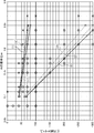
- FIG. 8 and 9 are graphs showing the relationship between the atomic ratio m (horizontal axis) of Al in the hard coating 20 and the bias voltage V (vertical axis) applied to the substrate 11.
- (2) ′ is a straight line of ⁇ 1556 m + 1022.6.
- the charged particles which are evaporated from the target 22 ⁇ / b> A and enter the base material 11 can be accelerated by the potential gradient formed in the vicinity of the base material 11, and energy can be applied.
- the magnetic field generating member 42 generates a magnetic field M extending from the target 22A toward the substrate 11 in a direction perpendicular to the discharge surface 22B.
- the hard coating 20 is formed.
- the discharge is stably maintained, and the generated plasma (ions, electrons) is less fluctuated and uniformized.
- the plasma generated by the magnetic field M lines of magnetic force
- the hard coating 20 can be formed stably and uniformly, and the hard coating 20 having a miniaturized cubic structure can be formed.
- the magnetic field M perpendicular to the discharge surface 22B of the target 22A is further increased. It can be easily generated.
- FIG. 10 shows a state in which a steel plate 60 that is a member to be pressed is installed in the mold 50.
- the mold 50 is a mold used for hot forming of the steel plate 60, for example, and is an upper mold 51 (first mold) and a lower mold 52 (second mold) that are spaced apart from each other in the vertical direction. Type).
- the upper die 51 has a convex portion 53
- the lower die 52 is formed with a concave portion 54 having a shape along the convex portion 53.
- the upper mold 51 and the lower mold 52 are configured to be movable in a direction approaching or separating from each other by a driving force from a driving source (not shown).
- a driving force from a driving source not shown.
- FIG. 10 by lowering the upper mold 51 in a state where the heated steel sheet 60 is placed on the molding surface of the lower mold 52, the steel sheet 60 is pressed by the convex portion 53. It can be formed into a shape along the recess 54 of the lower mold 52.
- a cold forming process may be performed.
- Each of the upper mold 51 and the lower mold 52 has base materials 55 and 58 constituting a main body portion of the mold, and hard films 56 and 57 coated on the surfaces of the base materials 55 and 58 by PVD. is doing. Similar to the first embodiment, the hard films 56 and 57 have a composition formula of Al m Cr 1-m N 1-xyZ C x B y O z (0.68 ⁇ m ⁇ 0.85). And having a cubic rock salt type crystal structure, H / E is 0.050 or more and 0.120 or less, and the hardness H is adjusted to 20 GPa or more and has excellent wear resistance. For this reason, not only the cutting tool illustrated in the first embodiment but also a plastic working jig such as the mold 50 can exhibit an excellent wear resistance effect.
- the mold 50 is not limited to the bending mold shown in FIG. 10, and may be another press mold such as a punching die, a drawing die, or a compression die.
- the hard film-coated member of the present invention can be applied to various machine parts that require wear resistance in addition to cutting tools and dies.
- it can be applied to sliding parts such as piston rings and valves.
- the base material 11 and the hard coating 20 are in direct contact with each other as shown in FIG. 3, and the base layer for improving the adhesion is between the base material 11 and the hard coating 20. It may be formed.
- the underlayer include those made of materials such as TiAlN, CrN, or TiN.
- the atomic ratio x of C may be outside the range of 0.05 ⁇ x ⁇ 0.5.
- the atomic ratio y of B may be less than 0.01.
- the atomic ratio z of O may be outside the range of z ⁇ 0.10.
- the hard coating 20 is formed by arc ion plating.
- the present invention is not limited to this, and the film may be formed by other physical vapor deposition methods such as sputtering.
- Example 1 [Hard film formation] First, various targets 22A having different Al contents (atomic ratio) were prepared, and the hard coating 20 was formed by changing the bias voltage (base bias) V applied to the base 11. The conditions of the Al atomic ratio m and the substrate bias V of the target 22A are as shown in Table 1 (Nos. 1 to 25) below. The film formation apparatus 2 described with reference to FIGS. 5 to 7 was used for film formation.
- a mirror-finished carbide test piece (13 mm ⁇ 13 mm ⁇ 5 mm thick) was prepared as the base material 11.
- the substrate 11 was ultrasonically cleaned in ethanol, introduced into the chamber 21, and set on the stage 24.
- a target 22A made of AlCr having the component composition shown in Table 1 was prepared and connected to the negative side of the arc power source 22.
- a target having a target diameter of 100 mm ⁇ was used as the target 22A.
- the inside of the chamber 21 was evacuated to 5 ⁇ 10 ⁇ 3 Pa, the substrate 11 was heated to 500 ° C. by the heater 26, and then etching with Ar ions was performed for 5 minutes. Thereafter, nitrogen gas was introduced until the inside of the chamber 21 reached 4 Pa. Then, the hard coating 20 was formed on the surface of the substrate 11 by evaporating the target 22A with a discharge current of 150A and rotating the stage 24 at a rotation speed of 5 rpm. At this time, the bias voltage V applied to the substrate 11 by the bias power source 25 was controlled as shown in Table 1 below. A DC power source was used as the bias power source 25. The film thickness of the hard coating 20 was 3 ⁇ m.
- the hardness was measured by a nanoindenter test using a cemented carbide test piece on which the hard coating 20 was formed.
- ENT-1100 manufactured by Elionix Co., Ltd. was used as the apparatus, and a Belkovic type triangular pyramid indenter was used as the indenter.
- Five load load curves were measured under five load conditions of 2 mN, 5 mN, 7 mN, 10 mN, and 20 mN, respectively.
- the data was corrected by the method (J. Mater. Res. Vol. 16, No. 11, 2001, 3084) proposed by SAWA et al.
- SAWA et al was calculated from the hardness and Young's modulus thus determined.
- the crystallinity of the hard coating 20 formed on the base material 11 is determined by X-ray diffraction (CuK ⁇ ray, 40 kV-40 mA, ⁇ -2 ⁇ , divergence slit 1 °, divergence length limiting slit 10 mm, scattering slit 1 °. , Light receiving slit 0.15 mm, monochrome light receiving slit 0.8 mm).
- a peak based on the cubic (111) plane in the hard coating 20 was observed at a diffraction angle (2 ⁇ ) of around 38 ° (36 to 39 °) in the X-ray diffraction pattern. The presence of this peak confirmed the formation of cubic crystals.
- FWHM Full Width Half Maximum
- the wear resistance of the hard coating 20 was confirmed by an MSE (Micro Slurry-Jet Erosion) test. About each sample which formed the hard film
- the MSE test uses a slurry (3 mass%) containing amorphous alumina particles of # 8000 (average particle size 1.2 ⁇ m), a projection distance of 10 mm, a projection angle of 90 °, and a projection pressure of 0.390 MPa ( ⁇ 0.002). Within the conditions).
- the slurry was projected for a certain period of time, and the erosion depth was determined by measuring the projection mark using a stylus roughness meter, and the erosion rate ( ⁇ m / min) was calculated. An erosion rate of 3.0 ⁇ 10 ⁇ 2 ⁇ m / min or less was accepted.
- the erosion rate increased with a decrease in the bias voltage (absolute value), and the wear resistance decreased. This is presumably because the energy given to the coating surface was reduced and hexagonal crystals were formed.
- the bias voltage exceeds the upper limit ( ⁇ 1429 m + 940.3), hexagonal crystals are formed even if the Al content is within the range of 0.70 ⁇ m ⁇ 0.85, and the wear resistance is poor. .
- the bias voltage was lower than the lower limit ( ⁇ 316 V), the effect of sputtering was increased, so that an evaluable film could not be formed.
- the graph of FIG. It corresponds to Examples 1 to 25, and “x” corresponds to a comparative example.
- Example 2 The conditions of the Al atomic ratio m and the substrate bias V of the target 22A were adjusted as shown in the following Table 2 and Table 3 (Nos. 1 to 47), and the same test as in Example 1 was performed.
- the bias voltage exceeds the upper limit ( ⁇ 214.3 m + 110), hexagonal crystals are formed even if the Al content is within the range of 0.7 ⁇ m ⁇ 0.85, and the wear resistance is poor. .
- the bias voltage is lower than the lower limit ( ⁇ 1666 m + 1100), the wear resistance is further improved when the bias voltage is higher than the lower limit.
- the graph of FIG. It corresponds to Examples 1 to 47, and “x” corresponds to a comparative example.
- the H / E is It turned out that the hard film 20 excellent in abrasion resistance adjusted to 0.058 or more and 0.120 or less can be formed.
- Example 1 is the same as Example 1 except that a hard film 20 containing the elements C, B, and O is formed.
- C and O were added into the film by introducing methane (CH 4 ) gas and oxygen (O) gas into the nitrogen gas during film formation.
- Boron (B) was added by putting it in the target 22A.
- the Al content was 71 at%, and the bias voltage applied to the substrate 11 was ⁇ 200V.
- Each evaluation method of the hard coating 20 was the same as that in Example 1. The test results are shown in Table 4 below. In Table 4, No. The result of 1 is indicated by a circle in the graph of FIG.
- Example 1 is the same as Example 1 except that a hard film 20 containing the elements C, B, and O is formed.
- C and O were added into the film by introducing methane (CH 4 ) gas and oxygen (O) gas into the nitrogen gas during film formation.
- Boron (B) was added by putting it in the target 41.
- the Al content was 77 at%, and the bias voltage applied to the substrate 11 was ⁇ 100V.
- Each evaluation method of the hard coating 20 was the same as that in Example 1. The test results are shown in Table 5 below.
Landscapes
- Engineering & Computer Science (AREA)
- Mechanical Engineering (AREA)
- Chemical & Material Sciences (AREA)
- Chemical Kinetics & Catalysis (AREA)
- Materials Engineering (AREA)
- Metallurgy (AREA)
- Organic Chemistry (AREA)
- Cutting Tools, Boring Holders, And Turrets (AREA)
- Physical Vapour Deposition (AREA)
Abstract
L'invention concerne un revêtement dur (20) comprenant chacun des éléments Al, Cr et N. Le revêtement dur (20) a une structure cristalline de type sel gemme cubique et comprend la formule de composition AlmCr1-mN1-x-y-zCxByOz (où 0,68 ≤ m ≤ 0,85 et y ≤ 0,10). Lorsque H (en GPa) représente la dureté du revêtement dur (20) et E (en GPa) représente le module de Young du revêtement dur (20), le rapport H/E de la dureté au module de Young est dans la plage de 0,050 à 0,120 inclus et H est d'au moins 20 GPa.
Applications Claiming Priority (4)
| Application Number | Priority Date | Filing Date | Title |
|---|---|---|---|
| JP2016062053A JP2017172022A (ja) | 2016-03-25 | 2016-03-25 | 硬質皮膜、硬質皮膜被覆部材及び硬質皮膜の製造方法 |
| JP2016-062053 | 2016-03-25 | ||
| JP2016196590A JP6789055B2 (ja) | 2016-10-04 | 2016-10-04 | 硬質皮膜、硬質皮膜被覆部材及び硬質皮膜の製造方法 |
| JP2016-196590 | 2016-10-04 |
Publications (1)
| Publication Number | Publication Date |
|---|---|
| WO2017163972A1 true WO2017163972A1 (fr) | 2017-09-28 |
Family
ID=59899432
Family Applications (1)
| Application Number | Title | Priority Date | Filing Date |
|---|---|---|---|
| PCT/JP2017/009922 Ceased WO2017163972A1 (fr) | 2016-03-25 | 2017-03-13 | Revêtement dur, élément recouvert de revêtement dur et procédé pour la production de revêtement dur |
Country Status (2)
| Country | Link |
|---|---|
| TW (1) | TW201804017A (fr) |
| WO (1) | WO2017163972A1 (fr) |
Cited By (4)
| Publication number | Priority date | Publication date | Assignee | Title |
|---|---|---|---|---|
| WO2020111122A1 (fr) * | 2018-11-29 | 2020-06-04 | 京セラ株式会社 | Outil revêtu et outil de coupe le comprenant |
| WO2020111123A1 (fr) * | 2018-11-29 | 2020-06-04 | 京セラ株式会社 | Outil à revêtement et outil de coupe le comprenant |
| DE112021001965T5 (de) | 2020-03-27 | 2023-01-12 | Kyocera Corporation | Beschichtetes werkzeug |
| JP2023172378A (ja) * | 2022-05-23 | 2023-12-06 | 国立大学法人福井大学 | 固体材料の表面内部評価方法 |
Families Citing this family (1)
| Publication number | Priority date | Publication date | Assignee | Title |
|---|---|---|---|---|
| JP7378716B2 (ja) * | 2018-10-24 | 2023-11-14 | 日東電工株式会社 | エンドミルの製造方法 |
Citations (6)
| Publication number | Priority date | Publication date | Assignee | Title |
|---|---|---|---|---|
| JP2003071611A (ja) * | 2001-06-19 | 2003-03-12 | Kobe Steel Ltd | 切削工具用硬質皮膜およびその製造方法並びに硬質皮膜形成用ターゲット |
| JP2004268250A (ja) * | 2003-02-17 | 2004-09-30 | Hitachi Tool Engineering Ltd | 被覆エンドミル及び被覆用ターゲット |
| JP2005344148A (ja) * | 2004-06-01 | 2005-12-15 | Sumitomo Electric Ind Ltd | 耐摩耗性被膜およびこれを用いた表面被覆切削工具 |
| JP2006524748A (ja) * | 2003-04-28 | 2006-11-02 | ユナキス・バルツェルス・アクチェンゲゼルシャフト | AlCr含有の硬質材料層を有する工作物および製造方法 |
| WO2012173236A1 (fr) * | 2011-06-17 | 2012-12-20 | 株式会社神戸製鋼所 | Élément recouvert d'un film de revêtement dur |
| JP2014091169A (ja) * | 2012-10-31 | 2014-05-19 | Mitsubishi Materials Corp | 表面被覆切削工具 |
-
2017
- 2017-03-13 WO PCT/JP2017/009922 patent/WO2017163972A1/fr not_active Ceased
- 2017-03-22 TW TW106109570A patent/TW201804017A/zh unknown
Patent Citations (6)
| Publication number | Priority date | Publication date | Assignee | Title |
|---|---|---|---|---|
| JP2003071611A (ja) * | 2001-06-19 | 2003-03-12 | Kobe Steel Ltd | 切削工具用硬質皮膜およびその製造方法並びに硬質皮膜形成用ターゲット |
| JP2004268250A (ja) * | 2003-02-17 | 2004-09-30 | Hitachi Tool Engineering Ltd | 被覆エンドミル及び被覆用ターゲット |
| JP2006524748A (ja) * | 2003-04-28 | 2006-11-02 | ユナキス・バルツェルス・アクチェンゲゼルシャフト | AlCr含有の硬質材料層を有する工作物および製造方法 |
| JP2005344148A (ja) * | 2004-06-01 | 2005-12-15 | Sumitomo Electric Ind Ltd | 耐摩耗性被膜およびこれを用いた表面被覆切削工具 |
| WO2012173236A1 (fr) * | 2011-06-17 | 2012-12-20 | 株式会社神戸製鋼所 | Élément recouvert d'un film de revêtement dur |
| JP2014091169A (ja) * | 2012-10-31 | 2014-05-19 | Mitsubishi Materials Corp | 表面被覆切削工具 |
Cited By (17)
| Publication number | Priority date | Publication date | Assignee | Title |
|---|---|---|---|---|
| JP7213888B2 (ja) | 2018-11-29 | 2023-01-27 | 京セラ株式会社 | 被覆工具およびそれを備えた切削工具 |
| KR102591245B1 (ko) | 2018-11-29 | 2023-10-19 | 교세라 가부시키가이샤 | 피복 공구 및 그것을 구비한 절삭 공구 |
| KR20210087049A (ko) * | 2018-11-29 | 2021-07-09 | 교세라 가부시키가이샤 | 피복 공구 및 그것을 구비한 절삭 공구 |
| KR20210087478A (ko) * | 2018-11-29 | 2021-07-12 | 교세라 가부시키가이샤 | 피복 공구 및 그것을 구비한 절삭 공구 |
| CN113165082A (zh) * | 2018-11-29 | 2021-07-23 | 京瓷株式会社 | 涂层刀具及具备该涂层刀具的切削刀具 |
| JPWO2020111123A1 (ja) * | 2018-11-29 | 2021-10-07 | 京セラ株式会社 | 被覆工具およびそれを備えた切削工具 |
| JPWO2020111122A1 (ja) * | 2018-11-29 | 2021-10-07 | 京セラ株式会社 | 被覆工具およびそれを備えた切削工具 |
| CN113165082B (zh) * | 2018-11-29 | 2025-02-21 | 京瓷株式会社 | 涂层刀具及具备该涂层刀具的切削刀具 |
| WO2020111123A1 (fr) * | 2018-11-29 | 2020-06-04 | 京セラ株式会社 | Outil à revêtement et outil de coupe le comprenant |
| US12151289B2 (en) | 2018-11-29 | 2024-11-26 | Kyocera Corporation | Coated tool and cutting tool including same |
| WO2020111122A1 (fr) * | 2018-11-29 | 2020-06-04 | 京セラ株式会社 | Outil revêtu et outil de coupe le comprenant |
| KR102676439B1 (ko) * | 2018-11-29 | 2024-06-19 | 교세라 가부시키가이샤 | 피복 공구 및 그것을 구비한 절삭 공구 |
| JP7441177B2 (ja) | 2018-11-29 | 2024-02-29 | 京セラ株式会社 | 被覆工具およびそれを備えた切削工具 |
| DE112021001965T5 (de) | 2020-03-27 | 2023-01-12 | Kyocera Corporation | Beschichtetes werkzeug |
| US12454012B2 (en) | 2020-03-27 | 2025-10-28 | Kyocera Corporation | Coated tool |
| JP7399504B2 (ja) | 2022-05-23 | 2023-12-18 | 国立大学法人福井大学 | 固体材料の表面内部評価方法 |
| JP2023172378A (ja) * | 2022-05-23 | 2023-12-06 | 国立大学法人福井大学 | 固体材料の表面内部評価方法 |
Also Published As
| Publication number | Publication date |
|---|---|
| TW201804017A (zh) | 2018-02-01 |
Similar Documents
| Publication | Publication Date | Title |
|---|---|---|
| JP6789055B2 (ja) | 硬質皮膜、硬質皮膜被覆部材及び硬質皮膜の製造方法 | |
| JP6268530B2 (ja) | 硬質被覆層がすぐれた耐チッピング性を発揮する表面被覆切削工具 | |
| CN106102972B (zh) | 被覆切削工具和其制造方法 | |
| JP5187570B2 (ja) | 硬質被覆層がすぐれた耐摩耗性を発揮する表面被覆切削工具 | |
| JP5621881B2 (ja) | 硬質皮膜被覆工具 | |
| JP2011189419A (ja) | 耐摩耗性に優れた被覆工具 | |
| WO2014132512A1 (fr) | Outil de coupe | |
| WO2014084338A1 (fr) | Outil de coupe à surface revêtue | |
| EP4292735A1 (fr) | Outil revêtu | |
| JP2016032861A (ja) | 被覆工具 | |
| TW201804017A (zh) | 硬質膜、硬質膜覆蓋構件及硬質膜之製造方法 | |
| WO2014142190A1 (fr) | Film dur, élément couvert d'un film dur, et procédé de fabrication du film dur et de l'élément couvert d'un film dur | |
| WO2021167087A1 (fr) | Outil revêtu | |
| Lu et al. | Characterization and wear role of (CrAlVTiNb) Nx high-entropy alloy nitride films deposited by high power impulse magnetron sputtering | |
| JP2017172022A (ja) | 硬質皮膜、硬質皮膜被覆部材及び硬質皮膜の製造方法 | |
| RU2715267C2 (ru) | Режущий инструмент с покрытием и способ | |
| KR20130028080A (ko) | 절삭 공구 | |
| CN108349016A (zh) | 表面包覆切削工具 | |
| JP6789503B2 (ja) | 硬質皮膜の成膜方法 | |
| JP6387190B2 (ja) | 被膜 | |
| JP5660457B2 (ja) | 硬質皮膜被覆金型 | |
| JP2015157975A (ja) | 硬質皮膜およびその形成方法 | |
| Yang et al. | Microstructure and mechanical properties of W–Ni–N coatings prepared by magnetron sputtering | |
| EP4082699B1 (fr) | Outil de coupe revêtu | |
| JP5617933B2 (ja) | 硬質皮膜被覆工具及びその製造方法 |
Legal Events
| Date | Code | Title | Description |
|---|---|---|---|
| NENP | Non-entry into the national phase |
Ref country code: DE |
|
| 121 | Ep: the epo has been informed by wipo that ep was designated in this application |
Ref document number: 17770015 Country of ref document: EP Kind code of ref document: A1 |
|
| 122 | Ep: pct application non-entry in european phase |
Ref document number: 17770015 Country of ref document: EP Kind code of ref document: A1 |