WO2017164211A1 - Film d'électrode réfléchissante stratifiée, motif d'électrode réfléchissante stratifiée et procédé de production d'un motif d'électrode réfléchissante stratifiée - Google Patents
Film d'électrode réfléchissante stratifiée, motif d'électrode réfléchissante stratifiée et procédé de production d'un motif d'électrode réfléchissante stratifiée Download PDFInfo
- Publication number
- WO2017164211A1 WO2017164211A1 PCT/JP2017/011347 JP2017011347W WO2017164211A1 WO 2017164211 A1 WO2017164211 A1 WO 2017164211A1 JP 2017011347 W JP2017011347 W JP 2017011347W WO 2017164211 A1 WO2017164211 A1 WO 2017164211A1
- Authority
- WO
- WIPO (PCT)
- Prior art keywords
- film
- reflective electrode
- atomic
- transparent conductive
- conductive oxide
- Prior art date
- Legal status (The legal status is an assumption and is not a legal conclusion. Google has not performed a legal analysis and makes no representation as to the accuracy of the status listed.)
- Ceased
Links
Images


Classifications
-
- H—ELECTRICITY
- H10—SEMICONDUCTOR DEVICES; ELECTRIC SOLID-STATE DEVICES NOT OTHERWISE PROVIDED FOR
- H10K—ORGANIC ELECTRIC SOLID-STATE DEVICES
- H10K50/00—Organic light-emitting devices
- H10K50/80—Constructional details
- H10K50/805—Electrodes
- H10K50/81—Anodes
- H10K50/818—Reflective anodes, e.g. ITO combined with thick metallic layers
-
- H—ELECTRICITY
- H05—ELECTRIC TECHNIQUES NOT OTHERWISE PROVIDED FOR
- H05B—ELECTRIC HEATING; ELECTRIC LIGHT SOURCES NOT OTHERWISE PROVIDED FOR; CIRCUIT ARRANGEMENTS FOR ELECTRIC LIGHT SOURCES, IN GENERAL
- H05B33/00—Electroluminescent light sources
- H05B33/10—Apparatus or processes specially adapted to the manufacture of electroluminescent light sources
-
- H—ELECTRICITY
- H05—ELECTRIC TECHNIQUES NOT OTHERWISE PROVIDED FOR
- H05B—ELECTRIC HEATING; ELECTRIC LIGHT SOURCES NOT OTHERWISE PROVIDED FOR; CIRCUIT ARRANGEMENTS FOR ELECTRIC LIGHT SOURCES, IN GENERAL
- H05B33/00—Electroluminescent light sources
- H05B33/12—Light sources with substantially two-dimensional [2D] radiating surfaces
- H05B33/26—Light sources with substantially two-dimensional [2D] radiating surfaces characterised by the composition or arrangement of the conductive material used as an electrode
Definitions
- the present invention relates to a laminated reflective electrode film that can be used, for example, as an anode of an organic electroluminescence (EL) element, a laminated reflective electrode pattern comprising the laminated reflective electrode film, and a method for producing the laminated reflective electrode pattern.
- EL organic electroluminescence
- an organic EL display is composed of organic EL elements arranged on a transparent substrate.
- An organic EL element is composed of an anode formed in a predetermined pattern on a transparent substrate, an organic EL light emitting layer, and a cathode. Holes are injected from the anode and electrons are injected from the cathode into the organic EL film.
- This is a light emitting element utilizing the principle of emitting light when holes and electrons are combined in the EL light emitting layer.
- the light extraction method of the organic EL element As the light extraction method of the organic EL element, a bottom emission method in which light is extracted from the transparent substrate side and a top emission method in which light is extracted from the side opposite to the transparent substrate are known.
- the top emission method since the top emission method has a higher aperture ratio than the bottom emission method, it is advantageous for high luminance.
- the anode used in the top emission type organic EL device has high reflectivity, high conductivity to efficiently extract light generated in the electroluminescent layer to the outside, and holes are efficiently formed in the electroluminescent layer. It is desirable that the work function be high so that it can be injected.
- Patent Documents 1 and 2 a laminated film having a work function increased by forming a surface oxide film by performing oxygen plasma treatment or the like on the surface of a metal film is used as an anode of an organic EL element.
- Patent Documents 3, 4, and 5 a laminated film in which a transparent conductive film such as an ITO film is formed on the surface of a metal film is used as an electrode of an organic EL element. Further, in Patent Document 6, a surface modified ITO film having a work function increased by irradiating the surface of the ITO film with oxygen ions or electrons to modify the surface is used as the anode of the organic EL element. ing.
- Patent Document 7 zinc oxide (ZnO), aluminum-added zinc oxide (AZO), and gallium are added as metal oxides in a laminated film in which a metal oxide thin film is stacked on a conductive layer containing Ag as a main component.
- the use of zinc oxide (GZO) is described.
- a metal oxide containing ZnO is easily dissolved in a resist stripping solution (weak alkali) used in an etching method. For this reason, it is difficult to form a laminated film using a metal oxide containing ZnO such as AZO or GZO into a fine electrode pattern that can be used as an electrode for an organic EL display by an etching method.
- JP 2006-294261 A International Publication No. 2010/032443 JP 2006-98856 A JP 2011-9790 A JP 2004-103247 A JP 2000-133466 A JP 2012-246511 A
- the above-described laminated reflective electrode film is required to have low electrical resistance and high reflectance equivalent to pure silver. Further, when manufacturing an organic EL element, it is necessary that a fine electrode pattern made of a laminated reflective electrode film can be easily formed by an etching method.
- the reflectance of visible light, particularly the reflectance of light in the blue region (400 to 500 nm) is lowered.
- the surface of the ITO film may be roughened and light may be scattered. It was.
- the electrode pattern is formed by etching in the laminated film of the Ag alloy film and the ITO film, the etching speed of the Ag alloy film is faster than that of the ITO film, so that the etching is performed collectively using the same etching solution. As a result, the Ag alloy film may be over-etched or an ITO film residue may be generated.
- the present invention has been made in view of the above-described circumstances, and is a laminated layer that has a high reflectance in the visible light region, particularly in the blue region, a low resistance value, and can easily form a fine electrode pattern by an etching method. It is an object of the present invention to provide a reflective electrode film, a laminated reflective electrode pattern comprising the laminated reflective electrode film, and a method for producing the laminated reflective electrode pattern.
- a laminated reflective electrode film of the present invention has an Ag film made of Ag or an Ag alloy, and a transparent conductive oxide film disposed on the Ag film, and the transparent conductive film
- the oxide film includes Zn and Ga, and further includes an oxide containing one or more of Sn, Y, and Ti.
- the laminated reflective electrode film of the present invention since the Ag film is provided, the electric resistance is lowered. Since the transparent conductive oxide film made of an oxide containing Zn and Ga and further containing one or more of Sn, Y and Ti is disposed on the Ag film, visible light, In particular, the reflectance of light in the blue region is increased. This is probably because the transparent conductive oxide film described above has a lower refractive index in the visible light region, particularly in the blue region than other transparent conductive oxides such as ITO. Moreover, since said transparent conductive oxide film contains 1 type, or 2 or more types in Sn, Y, and Ti, alkali resistance improves and it is hard to melt
- the laminated reflective electrode film of the present invention can form an electrode pattern by an etching method. Further, when an electrode pattern is formed by an etching method, when an acidic mixed solution containing phosphoric acid and acetic acid is used as an etchant for the above Ag film and the transparent conductive oxide film, a difference in etching rate occurs. Becomes smaller. Therefore, the multilayer reflective electrode film of the present invention reduces the amount of overetching when the electrode pattern is formed by the etching method. Note that since the transparent conductive oxide film has a work function higher than that of ITO, the transparent conductive oxide film can be used without performing surface modification by irradiation with oxygen ions or electrons.
- the atomic ratio of all metal elements contained in the transparent conductive oxide film is such that Ga is 0.5 atomic% or more and 30.0 atomic% or less, Sn, Y and Ti is preferably 0.1 atomic percent or more and 10.0 atomic percent or less, and the remaining Zn.
- the Ga content in all the metal elements contained in the transparent conductive oxide film is in the range of 0.5 atomic% or more and 30.0 atomic% or less, the increase in electric resistance is suppressed.
- the adhesion between the Ag film and the transparent conductive oxide film can be improved.
- the alkali resistance and environmental resistance are improved while suppressing the increase in electrical resistance.
- Y is more preferably contained in the transparent conductive oxide film 13 because the effect of improving alkali resistance is greater.
- the atomic ratio of all metal elements contained in the transparent conductive oxide film is such that Ga is 0.5 atomic% or more and 18.0 atomic% or less, Sn, Y and Ti Is more preferably 0.1 atomic percent or more and 10.0 atomic percent or less, and the remaining Zn.
- the Ga content in all the metal elements contained in the transparent conductive oxide film is in the range of 0.5 atomic% or more and 18.0 atomic% or less, an increase in electrical resistance is further suppressed. Meanwhile, the adhesion between the Ag film and the transparent conductive oxide film can be further improved.
- the total amount of Sn, Y and Ti is within the range of 0.1 atomic% or more and 10.0 atomic% or less, the alkali resistance and environmental resistance are improved while suppressing the increase in electrical resistance. Can be made.
- the atomic ratio of all metal elements contained in the transparent conductive oxide film is such that Ga is 0.5 atomic% or more and 14.0 atomic% or less, Sn, Y and More preferably, Ti is 0.1 atomic percent or more and 10.0 atomic percent or less, and the remaining Zn.
- the Ga content in all the metal elements contained in the transparent conductive oxide film is in the range of 0.5 atomic% or more and 14.0 atomic% or less, the increase in electrical resistance is further suppressed. Meanwhile, the adhesion between the Ag film and the transparent conductive oxide film can be further improved.
- the total amount of Sn, Y and Ti is within the range of 0.1 atomic% or more and 10.0 atomic% or less, the alkali resistance and environmental resistance are improved while suppressing the increase in electrical resistance. Can be made.
- the Ag film is composed of Cu, In, Sn, Sb, Ti, Mg, Zn, Ge, Al, Ga, Pd, Au, Pt, Bi, Mn, Sc, Y. , Nd, Sm, Eu, Gd, Tb, and Er containing a total of 0.2 atomic percent or more and 2.0 atomic percent or less, and the balance is an Ag alloy composed of Ag and inevitable impurities. It is preferable to be configured.
- the Ag film is made of Cu, In, Sn, Sb, Ti, Mg, Zn, Ge, Al, Ga, Pd, Au, Pt, Bi, Mn, Sc, Y, Nd, Sm, Eu, Gd, Tb. , Er or the like, the sulfidation resistance and heat resistance of the Ag film are improved, deterioration is prevented, and the film can be used stably for a long period of time.
- the thickness of the Ag film is 50 nm or more and the thickness of the transparent conductive oxide film is 100 nm or less.
- the thickness of the Ag film is 50 nm or more, the amount of visible light reflected on the surface of the Ag film is increased, and the reflectance of visible light is improved.
- the thickness of the transparent conductive oxide film is 100 nm or less, the visible light transmittance of the transparent conductive oxide film is improved, and the amount of visible light reflected on the surface of the Ag film is increased. .
- the multilayer reflective electrode pattern of the present invention is composed of the multilayer reflective electrode film described above and has a predetermined pattern. According to the multilayer reflective electrode pattern of the present invention, since it is composed of the multilayer reflective electrode film described above, the electrical resistance is low, and the reflectance of visible light, particularly light in the blue region, is high.
- the method for producing a laminated reflective electrode pattern according to the present invention is a method for producing the laminated reflective electrode pattern described above, wherein the laminated reflective electrode film includes the Ag film and the transparent conductive oxide film on a film forming surface of a substrate.
- a laminated reflective electrode film forming step for forming a film, a resist film forming step for forming a resist film having a predetermined pattern on the laminated reflective electrode film, and the laminated reflective electrode film on which the resist film is formed Using an acidic mixed solution containing phosphoric acid and acetic acid as an etchant, and an etching process for performing batch etching, and a resist film removing process for removing the resist film after etching. To do.
- the method for manufacturing a laminated reflective electrode pattern having this configuration when an acidic mixed solution containing phosphoric acid and acetic acid is used as an etchant, the difference in etching rate between the Ag film and the transparent conductive oxide film is small. Even if the laminated reflective electrode film is etched at once, the overetching of the Ag film, the residue of the transparent conductive oxide film, and the like can be suppressed, and the electrode pattern can be formed with high accuracy. In addition, since the alkali resistance of the transparent conductive oxide film is improved by adding one or more of Sn, Y and Ti, the resist film is removed using an alkaline resist removing solution in the resist film removing step. Even if it removes, degradation of the characteristic of a lamination reflective electrode pattern can be controlled.
- the method for producing a laminated reflective electrode pattern according to the present invention is a method for producing the laminated reflective electrode pattern described above, wherein a resist film forming step of forming a reverse pattern resist film having a predetermined pattern on the film-forming surface of the substrate; A laminated reflective electrode film forming step of forming the laminated reflective electrode film including the Ag film and the transparent conductive oxide film on a film forming surface of the base material on which the resist film is formed; and the resist film And a resist film removing step to be removed.
- a resist film is formed in a reverse pattern of a predetermined pattern on the film formation surface of the substrate, and the film formation surface of the substrate on which the resist film is formed A laminated reflective electrode film is formed.
- the resist film is removed from the substrate after forming the multilayer reflective electrode film, the multilayer reflective electrode film remains only in a region where the resist film is not formed and has a predetermined pattern. A pattern can be formed. For this reason, it is not necessary to perform an etching process, and a predetermined pattern can be formed with high accuracy.
- the alkali resistance of the transparent conductive oxide film is improved by adding one or more of Sn, Y, and Ti, a resist film is obtained using an alkaline resist removing solution in the resist film removing step. Even if it removes, degradation of the characteristic of a lamination reflective electrode pattern can be controlled.
- a laminated reflective electrode film having a high reflectance in the visible light region, particularly a blue region, a low resistance value, and a fine electrode pattern that can be easily formed by an etching method, and the laminated reflective electrode film are provided. It becomes possible to provide a manufacturing method of a laminated reflective electrode pattern and a laminated reflective electrode pattern.
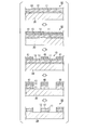
- the laminated reflective electrode film 10 in the present embodiment is used as an anode of an organic EL element, and is particularly used as an anode of a top emission type organic EL element.
- FIG. 1 shows a laminated reflective electrode film 10 according to this embodiment.
- the laminated reflective electrode film 10 includes, for example, a base oxide film 11 formed as a base layer formed on one surface of a substrate 20 as a base material, and an Ag film formed on the base oxide film 11. 12 and a transparent conductive oxide film 13 formed on the Ag film 12.
- a base oxide film 11 formed as a base layer formed on one surface of a substrate 20 as a base material
- substrate 20 a glass substrate, a resin film, etc. can be used, for example.
- the laminated reflective electrode film 10 having such a configuration has a high reflectance in the visible light region, particularly in the blue region, and a low resistance value.
- the reflectance of the laminated reflective electrode film 10 in the visible light region is preferably 95% or more, more preferably 96% or more, on average.
- the reflectance in the blue region (wavelength 400 to 500 nm) of the multilayer reflective electrode film 10 is preferably 86% or more on average and more preferably 88% or more.
- the higher the reflectivity, the better, so the upper limit is not particularly limited, but the reflectivity in the visible light region (wavelength 400 to 800 nm) is preferably 99% or less, and more preferably 98% or less.
- the reflectance in the blue region is preferably 95% or less, and more preferably 90% or less.
- the resistance value of the laminated reflective electrode film 10 is 1.0 ⁇ / sq. Or less, preferably 0.5 ⁇ / sq. More preferably, it is as follows. Since the sheet resistance value of the multilayer reflective electrode film 10 is preferably as low as possible, the lower limit value is not particularly limited, but is 0.1 ⁇ / sq. Is preferable, and 0.2 ⁇ / sq. Is more preferable.
- the base oxide film 11 is made of an oxide.
- the underlayer oxide film 11 has an action of suppressing deterioration of the Ag film 12 by suppressing intrusion of moisture and sulfur into the Ag film 12. Further, since the base oxide film 11 has higher adhesion to the Ag film 12 than the substrate 20, there is an effect of preventing the Ag film 12 from peeling off.
- the oxide constituting the base oxide film 11 the same oxide as that constituting the transparent conductive oxide film 13 can be used. However, it is not necessary to use an oxide having the same composition as that of the base oxide film 11. In the present embodiment, the transparent conductive oxide film 13 is composed of the same oxide.
- the Ag film 12 is made of Ag or an Ag alloy.
- the Ag or Ag alloy constituting the Ag film 12 is pure Ag having a purity of 99.9% by mass or more, or Cu, In, Sn, Sb, Ti, Mg, Zn, Ge, Al, Ga, Pd, Au. , Pt, Bi, Mn, Sc, Y, Nd, Sm, Eu, Gd, Tb, and an Ag alloy containing an additive element such as Er may be used.
- the content of the additive element is desirably limited to 2.0 atomic% or less from the viewpoint of suppressing a decrease in reflectance in the visible light region and an increase in electrical resistance of the Ag film 12.
- the Ag film 12 is formed of Cu, In, Sn, Sb, Ti, Mg, Zn, Ge, Al, Ga, Pd, Au, Pt, Bi, Mn, Sc, Y, Nd, Sm, One or more of Eu, Gd, Tb, and Er are contained in a total of 0.2 atomic% to 2.0 atomic%, and the balance is made of an Ag alloy made of Ag and inevitable impurities.
- Nd, Sm, Eu, Gd, Tb, and Er are elements having an effect of improving the sulfidation resistance and heat resistance of the Ag film 12, and suppress the deterioration of the Ag film 12 in the agglomeration production process and the use environment. It becomes possible.
- the reflectivity of the Ag film 12 may decrease and the resistance value may increase.
- Cu, In, Sn, Sb, Ti, Mg, Zn, Ge, Al, Ga, Pd, Au, Pt, Bi, Mn The total content of one or more of Sc, Y, Nd, Sm, Eu, Gd, Tb, and Er is specified within a range of 0.2 atomic% to 2.0 atomic%.
- the lower limit of the total content of one or more of Bi, Mn, Sc, Y, Nd, Sm, Eu, Gd, Tb, Er is 0.3 atomic% or more, 0.5 It is more preferable to set it to atomic% or more.
- the upper limit of the total content of one or more is preferably 1.8 atomic% or less, and is preferably 1.5 atomic% or less More preferably.
- the transparent conductive oxide film 13 is an oxide containing Zn and Ga and further containing one or more of Sn, Y and Ti. That is, the transparent conductive oxide film 13 is made by adding Ga and one or more of Sn, Y and Ti to Zn oxide.
- the atomic ratio between Ga in all the metal elements contained in the transparent conductive oxide film 13 and one or more of Sn, Y, and Ti is 0.5 atomic% or more. 30.0 atomic percent or less, Sn, Y, and Ti are 0.1 atomic percent or more and 10.0 atomic percent or less, respectively.
- the Ga content (atomic ratio of Ga to the total metal elements) in all the metal elements contained in the transparent conductive oxide film 13 to 0.5 atomic% or more, the Ag film 12 and the transparent conductive oxide are added. Together with improving the adhesion of the material film 13, an increase in electrical resistance in the transparent conductive oxide film 13 can be suppressed.
- the Ga content is 30.0 atomic% or less, an increase in electrical resistance in the transparent conductive oxide film 13 can be suppressed.
- the lower limit of the Ga content is preferably 1.0 atomic% or more, and more preferably 2.0 atomic% or more. preferable.
- the upper limit of the Ga content is preferably 25.0 atomic% or less, and preferably 20.0 atomic% or less. Is more preferably 18.0 atomic% or less, and even more preferably 14.0 atomic% or less.
- the alkali resistance and environmental resistance of the transparent conductive oxide film 13 are each set. Can be improved.
- the contents of Sn, Y and Ti are preferably contained in the transparent conductive oxide film 13 because the effect of improving alkali resistance is greater.
- the lower limit of each content of Sn, Y and Ti is 0.2 atomic% or more, More preferably, it is 0.5 atomic% or more.
- the upper limit of each content of Sn, Y and Ti is preferably 9.0 atomic% or less, and 8.0 atoms. % Or less is more preferable.
- the total content of Ga, Sn, Y and Ti is preferably 35.0 atomic% or less, preferably 30.0 atoms. % Or less, more preferably 25.0 atomic% or less.
- the film thickness t2 of the Ag film 12 is set to 50 nm or more in order to improve the reflectance.
- the thickness t2 of the Ag film 12 is preferably 60 nm or more, and more preferably 80 nm or more.
- the upper limit of the film thickness t2 of the Ag film 12 is not particularly limited, but the film thickness t2 of the Ag film 12 is preferably 200 nm or less, and more preferably 150 nm or less.
- the film thickness t3 of the transparent conductive oxide film 13 is set to 100 nm or less in order to improve the transmittance. In order to further improve the transmittance, t3 of the transparent conductive oxide film 13 is preferably 80 nm or less, and more preferably 50 nm or less. The lower limit of t3 of the transparent conductive oxide film 13 is preferably 5 nm.
- the film thickness t1 of the base oxide film 11 is not particularly limited, and may be the same as the film thickness t3 of the transparent conductive oxide film 13.
- the laminated reflective electrode pattern 30 according to the present embodiment is obtained by forming a predetermined pattern on the laminated reflective electrode film 10 shown in FIG.
- the pattern of the laminated reflective electrode pattern 30 according to the present embodiment is, for example, a pattern in which a plurality of rectangular electrode units having a side length of 10 ⁇ m to 500 ⁇ m are arranged on the substrate. is there.
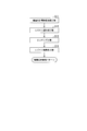
- the laminated reflective electrode pattern 30 described above is manufactured as follows. First, the multilayer reflective electrode film 10 according to the present embodiment is deposited on the film deposition surface of the substrate 20 as a base material (laminate reflective electrode film deposition step S11).
- a base oxide film 11 is formed on the substrate 20 as a base layer.
- the base oxide film 11 is preferably formed by DC sputtering using a sintered target whose film composition can be easily controlled.
- an Ag film 12 is formed on the formed base oxide film 11 by DC sputtering using an Ag target.
- This Ag target has a composition corresponding to the composition of the Ag film 12 to be formed.
- a transparent conductive oxide film 13 is formed on the formed Ag film 12 by DC sputtering using a transparent conductive oxide target.
- the transparent conductive oxide target is preferably a sintered target whose film composition can be easily controlled. In this way, the multilayer reflective electrode film 10 according to this embodiment is formed.
- a resist film 41 is formed on the multilayer reflective electrode film 10 formed on the surface of the substrate 20, and the resist film 41 is exposed and developed to form a multilayer reflective electrode pattern (resist film formation).
- the laminated reflective electrode film 10 on which the resist film 41 is formed is collectively etched using an acidic mixed solution containing phosphoric acid and acetic acid as an etchant (etching step S13).
- the content of phosphoric acid is preferably 55% by volume or less
- the content of acetic acid is preferably 30% by volume or less.
- the mixed solution may contain 20% by volume or less of nitric acid in addition to phosphoric acid and acetic acid.
- the resist film 41 is removed using an alkaline resist removing solution (resist film removing step S14). Thereby, the laminated reflective electrode film 10 located below the resist film 41 having the laminated reflective electrode pattern shape remains, and the laminated reflective electrode pattern 30 having a predetermined pattern is formed.
- a base oxide film 11 is formed as a base layer on the surface of the substrate 20, and an Ag film 12 is formed on the base oxide film 11. Is formed, water and sulfur can be prevented from entering the Ag film 12, and alteration of the Ag film 12 can be suppressed over a long period of time.
- the base oxide film 11 and the transparent conductive oxide film 13 are made by adding Ga or one or more of Sn, Y, and Ti to the Zn oxide, respectively.
- the atomic ratio of all metal elements contained in the oxide film is such that Ga is 0.5 atomic% to 30.0 atomic%, and Sn, Y, and Ti are 0.1 atomic% to 10.0 atomic%, respectively. Since the remaining Zn is used, the addition of Ga can improve the adhesion between the Ag film 12 and the transparent conductive oxide film 13, and can suppress an increase in electrical resistance. Moreover, alkali resistance can be improved by addition of Sn, Y and Ti. Furthermore, the base oxide film 11 and the transparent conductive oxide film 13 can suppress the intrusion of moisture and sulfur into the Ag film 12 and suppress the deterioration of the Ag film 12.
- the Ag film 12 is made of Cu, In, Sn, Sb, Ti, Mg, Zn, Ge, Al, Ga, Pd, Au, Pt, Bi, Mn, Sc, Y, Nd, Sm, Since one or more of Eu, Gd, Tb, and Er are contained in a total of 0.2 atomic percent to 2.0 atomic percent, and the balance is composed of an Ag alloy composed of Ag and inevitable impurities.
- the sulfidation resistance and heat resistance of the Ag film are improved, the deterioration is prevented, and the Ag film can be used stably for a long time.
- the laminated reflective electrode pattern 30 according to the present embodiment has a predetermined pattern formed on the laminated reflective electrode film 10 according to the present embodiment, it has a high reflectance with respect to light in the visible light region, particularly in the blue region. And a low resistance value.
- an organic EL display uses an organic EL element that emits blue light, an organic EL element that emits green light, and an organic EL element that emits red light, and combines the blue light, green light, and red light emitted from each organic EL element. Get an image. For this reason, when the reflectance of the blue region of the anode is lower than the reflectance of the green region or the red region, it is necessary to increase the power supplied to the organic EL element that emits blue light in order to increase the amount of blue light emission. was there.
- the multilayer reflective electrode pattern 30 according to the present embodiment has a high reflectance with respect to light in the blue region, it is not necessary to supply a large amount of power to the organic EL element that emits blue light. Since the deterioration is suppressed, the color balance of the entire organic EL display is stabilized over a long period of time.
- the etching of the Ag film 12, the base oxide film 11, and the transparent conductive oxide film 13 is performed. Since the difference in speed is small, it is possible to suppress the occurrence of over-etching of the Ag film 12 and residues of the base oxide film 11 and the transparent conductive oxide film 13 even when the laminated reflective electrode film 10 is collectively etched.
- the laminated reflective electrode pattern 30 can be formed with high accuracy.
- the alkali resistance of the transparent conductive oxide film 13 is improved by adding one or more of Sn, Y, and Ti. Therefore, in the resist film removing step S14, an alkaline resist is used. Even if the resist film is removed using the removing liquid, the deterioration of the characteristics of the laminated reflective electrode pattern can be suppressed.
- the Ag film 12 is made of Cu, In, Sn, Sb, Ti, Mg, Zn, Ge, Al, Ga, Pd, Au, Pt, Bi, Mn, Sc, Y, Nd, Sm, Eu. , Gd, Tb, and Er are included as a total of 0.2 atomic percent to 2.0 atomic percent, with the balance being composed of an Ag alloy composed of Ag and inevitable impurities.
- the present invention is not limited to this, and may be pure Ag or an Ag alloy containing other metal elements that are solid-solved in Ag.
- the base oxide film 11 has been described as being composed of the same oxide as the transparent conductive oxide film 13, but the present invention is not limited to this.
- ZnO, AZO or the like may be used.
- the base oxide film 11 is preferably composed of a film having a small difference in etching rate between the Ag film 12 and the transparent conductive oxide film 13.
- the base oxide film 11 is disposed as a base layer between the substrate 20 and the Ag film 12, but the present invention is not limited to this, and the Ag is directly formed on the surface of the substrate 20.
- a membrane 12 may be disposed.
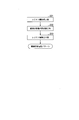
- the laminated reflective electrode pattern 30 has been described as being manufactured by an etching method, but the present invention is not limited to this, and as shown in FIGS. You may manufacture by the lift-off method.
- a resist film 41 is formed on the film-forming surface of the substrate 20, and the resist film 41 is exposed and developed to obtain a laminated reflective electrode.
- An inverted pattern obtained by inverting the pattern is formed (resist film forming step S21).
- the base oxide film 11, the Ag film 12, and the transparent conductive oxide film 13 are sequentially formed on the substrate 20 on which the resist film 41 having the reverse pattern is formed by a sputtering method.
- the laminated reflective electrode film 10 is formed on the resist film 41 and the substrate 20 (laminated reflective electrode film forming step S22).
- the resist film 41 is removed using an alkaline resist removing solution (resist film removing step S23).
- the laminated reflective electrode film 10 formed on the resist film 41 having the inverted pattern is removed, and a laminated reflective electrode pattern 30 having a predetermined pattern is formed.
- a predetermined pattern can be formed with high accuracy without performing an etching process.
- an alkaline resist removing solution is used in the resist film removing step S23. Even if the resist film is removed, the deterioration of the characteristics of the laminated reflective electrode pattern 30 can be suppressed.
- a laminated reflective electrode film having a structure shown in Table 1-5 was formed by sputtering.
- membrane and the transparent conductive oxide film in the Example of this invention and a comparative example was measured using the film thickness meter (DEKTAK by ULVAC).
- the compositions of the transparent conductive oxide film and the Ag alloy film were determined by quantitative analysis of elements using an ICP emission spectrometer (ICP emission spectrometer STS-3500DD manufactured by Hitachi High-Tech Science Co., Ltd.).
- the base oxide film and the transparent conductive oxide film For the production of the base oxide film and the transparent conductive oxide film, an oxide sintered body target having the composition described in Table 1-5 was used.
- the Ag film pure Ag or an Ag alloy target having the composition described in Table 1-5 was used.
- the composition of the ITO film (oxide in which Sn is added to In 2 O 3 ) in Table 5 is In: 35.6 atomic%, Sn: 3.6 atomic%, O: 60.8 Atomic%.
- the ITO film having the structure of Comparative Examples 1 to 5 was changed to a GZO film (the composition of the film was Zn: 47.3 atomic%, Ga: 2.2 atomic%) , O: 50.5 atomic%) was also produced.
- the conditions for forming each film are as follows.
- Sputtering device DC magnetron sputtering device (CS-200 manufactured by ULVAC) Magnetic field intensity: 1000 Gauss (directly above the target, vertical component) Ultimate vacuum: 5 ⁇ 10 ⁇ 5 Pa or less
- Sputtering gas Ar + O 2 mixed gas (O 2 mixing ratio 2%)
- Sputtering gas pressure 0.4 Pa
- Sputtering power DC100W
- Sputtering device DC magnetron sputtering device (CS-200 manufactured by ULVAC) Magnetic field intensity: 1000 Gauss (directly above the target, vertical component) Ultimate vacuum: 5 ⁇ 10 ⁇ 5 Pa or less Sputtering gas: Ar Sputtering gas pressure: 0.5 Pa Sputtering power: DC100W
- the evaluation method is as follows.
- Sheet resistance was measured by a four-probe method using a surface resistance measuring instrument (Loresta AP MCP-T400 manufactured by Mitsubishi Yuka Co., Ltd.). The measurement results are shown in Table 6-10, respectively.
- ⁇ Patterning test by etching method About the above-mentioned laminated reflective electrode film, a resist film was formed on the laminated reflective electrode film in the shape of an electrode pattern having a line width / space width of 30 ⁇ m / 30 ⁇ m by photolithography (photolithography). This was subjected to batch etching using a mixed solution containing phosphoric acid and acetic acid (SEA-5 manufactured by Kanto Chemical Co., Inc.) as an etchant. The etching was performed without heating and with an appropriate etching time (20 seconds to 240 seconds). Further, the phosphoric acid content in the mixed solution was 55% by volume or less, and the acetic acid content was 30% by volume or less.
- SEA-5 manufactured by Kanto Chemical Co., Inc.
- the formed electrode pattern was magnified with an optical microscope (Laser Microscope VK-X200 manufactured by KEYENCE). Observation was performed at 50 times, and the presence or absence of a residue of the transparent conductive oxide film 13 was confirmed. In addition, it is judged that there is a residue of the transparent conductive oxide film 13 when the presence of the transparent conductive oxide film that is not etched and remains in the form of needles or particles is recognized, and the rest is the transparent conductive oxide film It was judged that there were no 13 residues.
- the cross section of the electrode pattern before removing the resist film (the cross section perpendicular to the line and space and perpendicular to the film formation surface of the substrate 20) is scanned at a magnification of 50,000 using a scanning electron microscope (SU8000 manufactured by Hitachi High-Technologies Corporation). Observed at double.
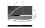
- the observation result of the cross-sectional shape of the electrode pattern obtained by the patterning test using the laminated reflective electrode film formed in Example 2 of the present invention is shown in FIG.
- the length L 2 of the length L 1 and the transparent conductive oxide film 13 of Ag film 12 is etched to the inside of the resist film 41 is measured, the length L 1 and length L 2 was calculated as the length of overetching.
- the length L 1 is the length between the end of the resist film 41 and the end of the Ag film 12 in the direction parallel to the film formation surface of the substrate 20, and the length L 2 is the film formation of the substrate 20. This is the length between the end of the resist film 41 and the end of the transparent conductive oxide film 13 in the direction parallel to the surface.
- the boundary (edge) of the resist pattern where the multilayer reflective electrode film 10 should remain between the substrate 20 is the end of the resist film 41, and the multilayer reflective electrode remaining between the resist pattern and the substrate 20
- the end of the Ag film 12 in the film 10 is the end of the Ag film 12, and the end of the transparent conductive oxide film 13 in the remaining laminated reflective electrode film 10 is the end of the transparent conductive oxide film 13. 1, was measured L 2.
- Table 6-10 shows the length of overetching for each sample of the present invention and the comparative examples. Note that the length of overetching in Table 6-10 is a value obtained by observing one cross section.
- ⁇ Patterning test by lift-off method First, a resist solution is applied to the substrate, a photomask on which an electrode pattern of line width / space width: 30 ⁇ m / 30 ⁇ m is attached, exposed to ultraviolet rays with an exposure machine, and then the portion exposed to the developer is removed. Then, a reversal pattern was formed by photolithography. Next, a multilayer reflective electrode film was formed on the substrate on which the reverse pattern was formed using the sputtering apparatus as described above.
- the formed electrode pattern was subjected to an optical microscope (KEYENCE).
- the accuracy of the electrode pattern was confirmed by observing at a magnification of 50 times with a laser microscope VK-X200 manufactured by the company.
- the average reflectance in the blue region and the average reflectance in the visible light region are 86% and 95% or more, respectively, and the sheet resistance after film formation is Except for the samples having the thickness of the Ag film of 50 nm (Invention Example 52, Invention Example 70), both are 0.5 ⁇ / sq. It was confirmed that a laminated film having excellent reflectance and sufficiently low resistance was obtained.
- the Ag film thickness is as thin as 50 nm, so the sheet resistance is 0.8 ⁇ / sq.
- the reflectivity was slightly reduced.
- the transparent conductive oxide film on the Ag film was thick as 100 nm and the absorption increased, so the reflectance was slightly smaller than that of the 10 nm sample.
- the average reflectance in the blue region and the average reflectance in the visible light region were smaller than 86% and 95%, respectively, and were lower than those of the present invention.
- the length of the overetching of the laminated film is 1 ⁇ m or less and there is no residue of the transparent conductive oxide film It was confirmed that the pattern can be formed with high accuracy.
- the length of overetching of the laminated film is larger than 1 ⁇ m, and a transparent conductive oxide film residue is generated. It was difficult to form the film with high accuracy.
- the patterning test by the lift-off method it was confirmed that the electrode pattern can be formed with high accuracy in the example of the present invention. Further, when the surface of the electrode pattern after the resist was peeled was visually observed, no change was observed in the present invention example as compared to before the test, whereas the GZO film without addition of Sn, Y, Ti was used.
- the laminated film of the comparative example which was a transparent conductive oxide, film peeling was observed in some places after resist peeling.
- the multilayer reflective electrode film of the present invention has a high reflectance in the visible light region, particularly in the blue region, a low resistance value, and a fine electrode pattern can be easily formed by an etching method, for example, organic electroluminescence (EL) Suitable for the anode of the element.
- EL organic electroluminescence
Landscapes
- Physics & Mathematics (AREA)
- Optics & Photonics (AREA)
- Engineering & Computer Science (AREA)
- Manufacturing & Machinery (AREA)
- Electroluminescent Light Sources (AREA)
Abstract
Priority Applications (4)
| Application Number | Priority Date | Filing Date | Title |
|---|---|---|---|
| CN201780018466.6A CN108886857B (zh) | 2016-03-23 | 2017-03-22 | 层叠反射电极膜、层叠反射电极图案及层叠反射电极图案的制造方法 |
| US16/086,623 US10971695B2 (en) | 2016-03-23 | 2017-03-22 | Multilayer reflection electrode film, multilayer reflection electrode pattern, and method of forming multilayer reflection electrode pattern |
| KR1020187025183A KR102327961B1 (ko) | 2016-03-23 | 2017-03-22 | 적층 반사 전극막, 적층 반사 전극 패턴, 적층 반사 전극 패턴의 제조 방법 |
| EP17770251.1A EP3435741B1 (fr) | 2016-03-23 | 2017-03-22 | Film d'électrode réfléchissante stratifiée, motif d'électrode réfléchissante stratifiée et procédé de production d'un motif d'électrode réfléchissante stratifiée |
Applications Claiming Priority (4)
| Application Number | Priority Date | Filing Date | Title |
|---|---|---|---|
| JP2016059097 | 2016-03-23 | ||
| JP2016-059097 | 2016-03-23 | ||
| JP2017-024269 | 2017-02-13 | ||
| JP2017024269A JP6776931B2 (ja) | 2016-03-23 | 2017-02-13 | 積層反射電極膜、積層反射電極パターン、積層反射電極パターンの製造方法 |
Publications (1)
| Publication Number | Publication Date |
|---|---|
| WO2017164211A1 true WO2017164211A1 (fr) | 2017-09-28 |
Family
ID=59899455
Family Applications (1)
| Application Number | Title | Priority Date | Filing Date |
|---|---|---|---|
| PCT/JP2017/011347 Ceased WO2017164211A1 (fr) | 2016-03-23 | 2017-03-22 | Film d'électrode réfléchissante stratifiée, motif d'électrode réfléchissante stratifiée et procédé de production d'un motif d'électrode réfléchissante stratifiée |
Country Status (1)
| Country | Link |
|---|---|
| WO (1) | WO2017164211A1 (fr) |
Cited By (2)
| Publication number | Priority date | Publication date | Assignee | Title |
|---|---|---|---|---|
| CN110165070A (zh) * | 2018-12-14 | 2019-08-23 | 合肥视涯显示科技有限公司 | Oled阳极的制作方法及oled显示装置的制作方法 |
| US20240172475A1 (en) * | 2022-11-18 | 2024-05-23 | Hannstar Display Corporation | Etching solution and manufacturing method of display panel |
Citations (11)
| Publication number | Priority date | Publication date | Assignee | Title |
|---|---|---|---|---|
| JP2000133466A (ja) | 1998-10-23 | 2000-05-12 | Canon Inc | 表面改質ito膜、その表面処理方法およびそれを用いた電荷注入型発光素子 |
| JP2002363732A (ja) * | 2001-03-15 | 2002-12-18 | Asahi Glass Co Ltd | 透明導電膜の製造方法および透明導電膜付き透明基板 |
| JP2004103247A (ja) | 2002-09-04 | 2004-04-02 | Sony Corp | 有機el表示装置 |
| JP2006098856A (ja) | 2004-09-30 | 2006-04-13 | Ulvac Japan Ltd | Ag系反射膜およびその作製方法 |
| JP2006294261A (ja) | 2005-04-05 | 2006-10-26 | Fuji Electric Holdings Co Ltd | 有機el発光素子およびその製造方法 |
| WO2010032443A1 (fr) | 2008-09-19 | 2010-03-25 | パナソニック株式会社 | Élément électroluminescent organique et son procédé de fabrication |
| JP2011009790A (ja) | 2000-02-03 | 2011-01-13 | Semiconductor Energy Lab Co Ltd | 発光装置 |
| JP2012246511A (ja) | 2011-05-25 | 2012-12-13 | Geomatec Co Ltd | 金属薄膜積層基板の製造方法及び静電容量型タッチパネルの製造方法 |
| JP2013105546A (ja) * | 2011-11-10 | 2013-05-30 | Ulvac Japan Ltd | 有機el表示装置、led装置、太陽電池、反射膜 |
| JP2015178239A (ja) * | 2014-03-19 | 2015-10-08 | 三菱マテリアル株式会社 | 積層膜 |
| JP2016085970A (ja) * | 2014-10-23 | 2016-05-19 | 株式会社半導体エネルギー研究所 | 発光素子、発光装置、表示装置、電子機器、及び照明装置 |
-
2017
- 2017-03-22 WO PCT/JP2017/011347 patent/WO2017164211A1/fr not_active Ceased
Patent Citations (11)
| Publication number | Priority date | Publication date | Assignee | Title |
|---|---|---|---|---|
| JP2000133466A (ja) | 1998-10-23 | 2000-05-12 | Canon Inc | 表面改質ito膜、その表面処理方法およびそれを用いた電荷注入型発光素子 |
| JP2011009790A (ja) | 2000-02-03 | 2011-01-13 | Semiconductor Energy Lab Co Ltd | 発光装置 |
| JP2002363732A (ja) * | 2001-03-15 | 2002-12-18 | Asahi Glass Co Ltd | 透明導電膜の製造方法および透明導電膜付き透明基板 |
| JP2004103247A (ja) | 2002-09-04 | 2004-04-02 | Sony Corp | 有機el表示装置 |
| JP2006098856A (ja) | 2004-09-30 | 2006-04-13 | Ulvac Japan Ltd | Ag系反射膜およびその作製方法 |
| JP2006294261A (ja) | 2005-04-05 | 2006-10-26 | Fuji Electric Holdings Co Ltd | 有機el発光素子およびその製造方法 |
| WO2010032443A1 (fr) | 2008-09-19 | 2010-03-25 | パナソニック株式会社 | Élément électroluminescent organique et son procédé de fabrication |
| JP2012246511A (ja) | 2011-05-25 | 2012-12-13 | Geomatec Co Ltd | 金属薄膜積層基板の製造方法及び静電容量型タッチパネルの製造方法 |
| JP2013105546A (ja) * | 2011-11-10 | 2013-05-30 | Ulvac Japan Ltd | 有機el表示装置、led装置、太陽電池、反射膜 |
| JP2015178239A (ja) * | 2014-03-19 | 2015-10-08 | 三菱マテリアル株式会社 | 積層膜 |
| JP2016085970A (ja) * | 2014-10-23 | 2016-05-19 | 株式会社半導体エネルギー研究所 | 発光素子、発光装置、表示装置、電子機器、及び照明装置 |
Non-Patent Citations (1)
| Title |
|---|
| JAPANESE SOCIETY FOR THE PROMOTION OF SCIENCE: "Technology of Transparent Conductive Films (Second Revised Edition)", 20 December 2006, OHMSHA LTD., pages: 171 - 172 |
Cited By (2)
| Publication number | Priority date | Publication date | Assignee | Title |
|---|---|---|---|---|
| CN110165070A (zh) * | 2018-12-14 | 2019-08-23 | 合肥视涯显示科技有限公司 | Oled阳极的制作方法及oled显示装置的制作方法 |
| US20240172475A1 (en) * | 2022-11-18 | 2024-05-23 | Hannstar Display Corporation | Etching solution and manufacturing method of display panel |
Similar Documents
| Publication | Publication Date | Title |
|---|---|---|
| CN108886857B (zh) | 层叠反射电极膜、层叠反射电极图案及层叠反射电极图案的制造方法 | |
| JP6888318B2 (ja) | 積層透明導電膜、積層配線膜及び積層配線膜の製造方法 | |
| JP5171990B2 (ja) | Cu合金膜および表示装置 | |
| JP2004158442A (ja) | 積層体、配線付き基体、有機el表示素子、有機el表示素子の接続端子及びそれらの製造方法 | |
| JP6870332B2 (ja) | 積層透明導電膜、積層配線膜及び積層配線膜の製造方法 | |
| CN104347818B (zh) | 发光装置及其制作方法 | |
| CN112018260B (zh) | 反射阳极电极、薄膜晶体管、有机el显示器及溅镀靶材 | |
| WO2017164211A1 (fr) | Film d'électrode réfléchissante stratifiée, motif d'électrode réfléchissante stratifiée et procédé de production d'un motif d'électrode réfléchissante stratifiée | |
| KR20190097919A (ko) | 은 박막 식각액 조성물 및 이를 이용한 식각 방법 및 금속 패턴의 형성 방법 | |
| JP4655281B2 (ja) | 薄膜配線層 | |
| KR101935131B1 (ko) | 은 함유 박막 식각액 조성물 및 이를 이용한 표시장치용 어레이기판의 제조방법 | |
| KR102623991B1 (ko) | 은 함유 박막 식각액 조성물 및 이를 이용하여 제조된 표시장치용 어레이기판 및 이의 제조방법 | |
| WO2017131183A1 (fr) | Film conducteur transparent multicouche, film de câblage multicouche et procédé de fabrication de film de câblage multicouche | |
| WO2016136953A1 (fr) | Fil conducteur transparent et procédé de fabrication de fil conducteur transparent | |
| WO2017164209A1 (fr) | Film conducteur transparent stratifié, film de câblage stratifié, et procédé de fabrication d'un film de câblage stratifié | |
| KR20190076494A (ko) | 은 함유 박막 식각액 조성물 및 이를 이용한 표시장치용 어레이기판의 제조방법 | |
| JP6123285B2 (ja) | 積層膜 | |
| KR20190000331A (ko) | 은 함유 박막 식각액 조성물 및 이를 이용한 표시장치용 어레이기판의 제조방법 | |
| KR20200060230A (ko) | 은 박막 식각액 조성물 및 이를 이용한 식각 방법 및 금속 패턴의 형성 방법 | |
| KR20200054813A (ko) | 은 박막 식각액 조성물 및 이를 이용한 식각 방법 및 금속 패턴의 형성 방법 | |
| KR20190076496A (ko) | 은 함유 박막 식각액 조성물 및 이를 이용한 표시장치용 어레이기판의 제조방법 |
Legal Events
| Date | Code | Title | Description |
|---|---|---|---|
| ENP | Entry into the national phase |
Ref document number: 20187025183 Country of ref document: KR Kind code of ref document: A |
|
| NENP | Non-entry into the national phase |
Ref country code: DE |
|
| WWE | Wipo information: entry into national phase |
Ref document number: 2017770251 Country of ref document: EP |
|
| ENP | Entry into the national phase |
Ref document number: 2017770251 Country of ref document: EP Effective date: 20181023 |
|
| 121 | Ep: the epo has been informed by wipo that ep was designated in this application |
Ref document number: 17770251 Country of ref document: EP Kind code of ref document: A1 |