WO2017164262A1 - Dispositif de type plaque mince - Google Patents
Dispositif de type plaque mince Download PDFInfo
- Publication number
- WO2017164262A1 WO2017164262A1 PCT/JP2017/011557 JP2017011557W WO2017164262A1 WO 2017164262 A1 WO2017164262 A1 WO 2017164262A1 JP 2017011557 W JP2017011557 W JP 2017011557W WO 2017164262 A1 WO2017164262 A1 WO 2017164262A1
- Authority
- WO
- WIPO (PCT)
- Prior art keywords
- conductive
- touch
- card
- conductor
- area
- Prior art date
- Legal status (The legal status is an assumption and is not a legal conclusion. Google has not performed a legal analysis and makes no representation as to the accuracy of the status listed.)
- Ceased
Links
Images























































Classifications
-
- G—PHYSICS
- G06—COMPUTING OR CALCULATING; COUNTING
- G06F—ELECTRIC DIGITAL DATA PROCESSING
- G06F3/00—Input arrangements for transferring data to be processed into a form capable of being handled by the computer; Output arrangements for transferring data from processing unit to output unit, e.g. interface arrangements
- G06F3/01—Input arrangements or combined input and output arrangements for interaction between user and computer
- G06F3/03—Arrangements for converting the position or the displacement of a member into a coded form
- G06F3/041—Digitisers, e.g. for touch screens or touch pads, characterised by the transducing means
-
- G—PHYSICS
- G06—COMPUTING OR CALCULATING; COUNTING
- G06F—ELECTRIC DIGITAL DATA PROCESSING
- G06F3/00—Input arrangements for transferring data to be processed into a form capable of being handled by the computer; Output arrangements for transferring data from processing unit to output unit, e.g. interface arrangements
- G06F3/01—Input arrangements or combined input and output arrangements for interaction between user and computer
- G06F3/03—Arrangements for converting the position or the displacement of a member into a coded form
- G06F3/033—Pointing devices displaced or positioned by the user, e.g. mice, trackballs, pens or joysticks; Accessories therefor
- G06F3/039—Accessories therefor, e.g. mouse pads
- G06F3/0393—Accessories for touch pads or touch screens, e.g. mechanical guides added to touch screens for drawing straight lines, hard keys overlaying touch screens or touch pads
-
- G—PHYSICS
- G06—COMPUTING OR CALCULATING; COUNTING
- G06F—ELECTRIC DIGITAL DATA PROCESSING
- G06F3/00—Input arrangements for transferring data to be processed into a form capable of being handled by the computer; Output arrangements for transferring data from processing unit to output unit, e.g. interface arrangements
- G06F3/01—Input arrangements or combined input and output arrangements for interaction between user and computer
- G06F3/03—Arrangements for converting the position or the displacement of a member into a coded form
- G06F3/041—Digitisers, e.g. for touch screens or touch pads, characterised by the transducing means
- G06F3/044—Digitisers, e.g. for touch screens or touch pads, characterised by the transducing means by capacitive means
Definitions
- the present invention relates to a device and a thin plate device.
- the recognition of the conductive pattern formed on the touch card is unstable, and the type of electronic device (smartphone or tablet, what type of smartphone, etc.) and usage environment (when electronic stamps are used, the electronic device must be handled manually. Or the like, etc.), the recognition accuracy of the conductor arrangement pattern is not stable.
- the present invention has been made in view of such a situation, and stably recognizes a conductive pattern formed on a card, and not only touches an electronic device but also points from an electronic device.
- Another object of the present invention is to provide a touch card that allows various authentication and content browsing by tapping with a conductor.
- an apparatus includes: An arrival amount detection unit for detecting an arrival amount per unit time of external energy coming from outside; An information acquisition circuit for acquiring input information in a predetermined format based on a change in the amount of arrival per unit time; A working surface on which one or more elements that cause a change in physical quantity detectable from the opposing surface are arranged; One or more physical quantity controllers that cause the physical quantity change in each of the one or more elements; An information output unit configured to output the output information in a predetermined format from the one or more elements according to the physical quantity change.
- an apparatus includes: For example, an identification information storage unit that stores identification information for identifying the device of one embodiment of the present invention described above as another device; A coding information generating circuit for generating coding information based on the identification information and the acquired input information; The information output unit outputs output information including the encoded information.
- the code even if the code is sequentially changed, it can be recognized by an electronic device such as a smartphone.
- FIG. 1 It is a figure which shows the usage example of a card type apparatus. It is a block diagram which shows the hardware structural example of an information device. It is a figure which illustrates the structure of the back surface of the card
- FIG. 38 is a diagram illustrating an exemplary arrangement of pattern codes according to the nineteenth embodiment.
- FIG. 38 is a diagram illustrating an exemplary arrangement of pattern codes according to the nineteenth embodiment.
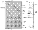
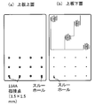
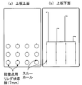
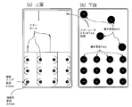
- (A) is a figure which illustrates the composition of the upper layer surface of the device of an embodiment
- (B) is the figure which combined the partial sectional view of the device.
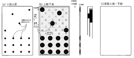
- (A) is a figure which illustrates the structure of the joint surface before element formation in a lower dielectric layer
- (B) is sectional drawing of an apparatus.
- (A) is a figure which illustrates the structure of the joint surface after element formation in the lower dielectric layer
- (B) is sectional drawing of an apparatus.
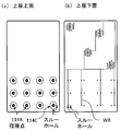
- (A) is a figure which illustrates the composition of the back of the device of an embodiment
- (B) is a figure which illustrates the outline of the section of the device after joining the dielectric of an upper layer and a lower layer.
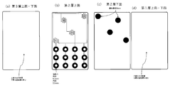
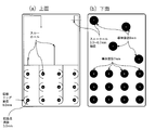
- (A) is a figure which illustrates the top view of the joint surface of the upper layer of the dielectric layer of the apparatus of embodiment
- (B) is the figure which combined the sectional view of the apparatus virtually.
- (A) is a figure which illustrates the state which formed the element in the lower dielectric back surface
- (B) is a figure which illustrates the state in which the element was formed in the lower dielectric back surface.
- (A) is a figure which illustrates the composition of the back of the device of an embodiment
- (B) is a figure which illustrates the outline of the section of the device after joining the dielectric of an upper layer and a lower layer.
- (A) is a figure which illustrates the composition of the upper layer surface of the device of an embodiment
- (B) is the figure which combined the partial sectional view of the device.
- (A) is a top view which illustrates the junction surface of the lower layer of the dielectric layer of an apparatus
- (B) is the figure which combined the partial cross section figure of the apparatus.
- (A) is a figure which illustrates the structure of the back surface of the apparatus after joining an upper layer and a lower layer
- (B) is a figure which illustrates the outline
- (A) is a figure which illustrates the composition of the upper layer surface of the device of an embodiment
- (B) is the figure which combined the partial sectional view of the device.
- (A) is a figure which illustrates the structure of the lower layer joining surface of an apparatus
- (B) is the figure which combined the partial cross section figure of the apparatus.
- (A) is a top view which illustrates the structure of the back surface of the apparatus which joined the upper layer and the lower layer
- (B) is a figure which shows the outline
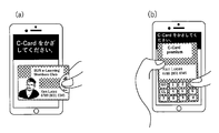
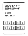
- C-Card is used as a credit card with a numeric keypad.
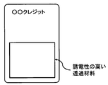
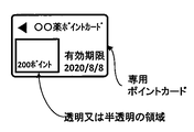
- C-Card is used as a credit card with a transparent area.
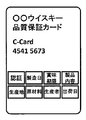
- C-Card is attached to a product package. It is a figure explaining the case where C-Card is used for authentication of a ticket and a coupon.
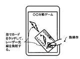
- C-Card is used as a game card. It is a figure explaining the state which is playing the game using the card for games.
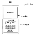
- C-Card is used as an authentication card.
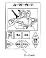
- C-Card is used as a movie card.
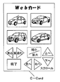
- C-Card is used as a Web card.
- C-Card is used as an examination ticket.
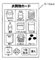
- C-Card is used as a shopping card.
- C-Card is used as a bank ATM card.
- C-Card is used as an animal card.
- C-Card is used as a questionnaire card.
- C-Card is used as a system control card.
- FIG. 1 shows an example of use of the card type device 110.
- the card-type device 110 has a configuration in which a conductive element is embedded in a plastic or paper plate member.
- the card-type device 110 is used in contact with a touch panel of an information device 200 such as a mobile phone, a smart phone, a portable information terminal, a tablet terminal personal computer, or an on-vehicle device.
- an information device 200 such as a mobile phone, a smart phone, a portable information terminal, a tablet terminal personal computer, or an on-vehicle device.
- FIG. 2 is a block diagram illustrating a hardware configuration example of the information device 200.
- the information device 200 includes a CPU 51, a ROM (Read Only Memory) 52, a RAM (Random Access Memory) 53, a bus 54, an input / output interface 55, a touch operation input unit 56, a display unit 57, and an input unit. 58, a storage unit 59, a communication unit 60, and a drive 61.
- ROM Read Only Memory
- RAM Random Access Memory
- the CPU 51 executes various processes according to a program recorded in the ROM 52 or a program loaded from the storage unit 59 to the RAM 53.
- the RAM 53 appropriately stores data necessary for the CPU 51 to execute various processes.
- the CPU 51, ROM 52 and RAM 53 are connected to each other via a bus 54.
- An input / output interface 55 is also connected to the bus 54.
- a touch operation input unit 56, a display unit 57, an input unit 58, a storage unit 59, a communication unit 60, and a drive 61 are connected to the input / output interface 55.
- the touch operation input unit 56 includes, for example, a capacitance type position input sensor stacked on the display surface of the display unit 57, and detects the coordinates of the position where the touch operation is performed.
- the touch operation refers to an operation of touching or approaching an object with respect to the touch operation input unit 56.
- An object that contacts or approaches the touch operation input unit 56 is generally a user's finger, a touch pen, or the like, and is a plurality of dots that configure the code output unit 13 of the code generator 1 in the present embodiment.
- touch position the position where the touch operation is performed
- touch coordinates the coordinates of the touch position
- the display unit 57 is composed of a display such as a liquid crystal display, and displays various images such as the images shown in FIGS.
- the touch operation input unit 56 and the display unit 57 constitute the touch panel 31 described above.
- the input unit 58 is composed of various hardware buttons and the like, and inputs various information according to the player's instruction operation.
- the storage unit 59 is composed of a DRAM (Dynamic Random Access Memory) or the like, and stores various data.
- DRAM Dynamic Random Access Memory
- the communication unit 60 controls communication with other devices (the server 4 in the example of FIG. 1) via the network N including the Internet.
- the drive 61 is provided as necessary.
- a removable medium 71 made of a magnetic disk, an optical disk, a magneto-optical disk, a semiconductor memory, or the like is appropriately attached to the drive 61.
- the program read from the removable medium 71 by the drive 61 is installed in the storage unit 59 as necessary.
- the removable medium 71 can also store various data stored in the storage unit 59 in the same manner as the storage unit 59.
- FIG. 3 is a diagram showing the structure of the card type device.
- the element 111 (conductor) is formed (including printing) with a unique pattern without electrically turning the conductor ON / OFF, and a region operated by a finger is provided.
- the region operated by the finger is configured such that the conductor gives the touch panel an interaction with a capacitance or electric field that can be detected by the touch panel.
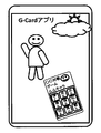
- FIG. 3 and 4 illustrate the configuration of the game cards.
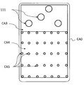
- FIG. 3 illustrates the configuration of the back surface of the card (the surface that contacts the touch panel).
- FIG. 4 illustrates the configuration of the surface of the card.
- This card is provided with a conductor corresponding to the element 111 and a conductor plate inside the card for connecting the conductor.
- the number of simultaneously recognizable by multi-touch on the touch panel of the information device 200 is five as in the case of current smartphones.
- a game program using the card can be executed while enabling operation with a finger.
- the touch panel recognizes a unique pattern code and specifies the type of card and the arrangement on the touch panel. In this case, the touch panel can recognize one touch at a rear position. Therefore, the remaining touch recognition is performed when the user presses the touch panel with a finger over the card (that is, from the upper side of the card).
- the information device 200 recognizes the type and arrangement of the card by the arrangement pattern of the element 111 (conductor) on the back surface. Therefore, each time the touch area TC1 is pressed, the information device 200 recognizes the position of the touch area TC1 in the pressed card and specifies the label. For example, when “walking” is pressed, the information device 200 that executes the game program executes an operation of walking “ ⁇ character” corresponding to the type of card on the display.
- FIG. 5 shows an example of using a card in a tablet terminal.
- the number of touches that can be simultaneously recognized by the touch panel is 5 places and 10 places, but these restrictions are examples. Therefore, the implementation of the present invention is not limited by the number of touches that can be simultaneously recognized by the touch panel.
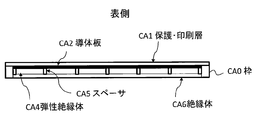
- FIG. 6 is a cross-sectional view (hereinafter referred to as cross-section A) in which the card is cut along a plane perpendicular to the paper surface passing through a line connecting the arrows A1 and A2 in FIG.
- FIG. 7 is a cross-sectional view (hereinafter referred to as cross-section B) in which the card is cut along a plane that passes through the line connecting the arrows B1 and B2 in FIG. 8 is a plan view (referred to as a bottom view) of the card of FIG. 3 viewed from below (the back side where the card contacts the touch panel).
- the card has a three-layer structure in general by a protective / printing layer CA1 on the front side, an internal conductor plate CA2 and an insulator CA3 (or elastic insulator CA4) on the back side.
- the periphery of the card is surrounded by an insulating frame.
- the element 111 in the vicinity of the cross section A, is embedded in the backside insulator CA3 and connected to the internal conductor plate CA2.
- the portion of the insulator CA3 in FIG. 6 is a portion where the presence or change of physical quantities (capacitance, electric field strength, etc.) is not detected by the touch panel.
- the touch panel detects the arrangement of the element 111 (conductor) from the presence or change of physical quantities (capacitance, electric field strength, etc.). If the arrangement of the element 111 (conductor) is asymmetric, the information device 200 acquires the arrangement coordinates of the element 111 (conductor) detected by the touch panel. Therefore, if the arrangement of the elements 111 (conductors) for each card is unique for a plurality of cards, the information device 200 can identify the type of the card.
- the protection / printing layer CA1 can be formed of a conductive material such as a conductive ink
- the user's finger touches the surface of the card, and the element is passed through the protection / printing layer CA1 and the conductor plate CA2.
- 111 conductor
- the protective / printing layer CA1 is not a conductive material, if the thickness is sufficiently thin and about 0.5 to 0.6 mm, the user can touch the protective / printing layer CA1 with the finger. , Causing electrostatic induction to the conductor plate CA2, and causing the touch panel to recognize the presence or change of a physical quantity (capacitance, electric field strength accompanying electrostatic induction) from the element 111 (conductor) through the conductor plate CA2.
- a conductive portion for example, conductive An ink thin film
- all the elements 111 may be connected to the conductive portions of these touch regions TC1 by conductive wires.
- a layer of an elastic insulator CA4 and a layer of an insulator CA6 are provided below the conductor plate CA2.
- a spacer CA5 is embedded in the layer of the elastic insulator CA4.
- the elastic insulator CA4 may be a gap, that is, an air layer.
- the elastic insulator CA4 may be a honeycomb structure or a layer formed of a sponge-like material.
- the spacer CA5 does not have to be cylindrical, and may have any shape as long as the structure supports the conductive plate CA2 with respect to the touch panel surface.
- the spacer CA5 may be, for example, a quadratic curved surface obtained by rotating a quadratic curve such as a hemisphere or a parabola.
- the spacer CA5 may be an elastic material.
- the spacer CA5 has elasticity, when the user presses the touch area TC1 (for example, a “walking” label), the conductive plate CA2 at the pressed position can easily come into contact with the touch panel, and the operability of the user is improved. To do.
- the conductive plate CA2 and the backside insulator CA6 come into contact with each other.
- the insulator CA6 may not be provided.
- the conductive plate CA2 contacts or approaches the touch panel surface. Accordingly, when the finger touches the touch area TC1, the conductive plate CA2 comes into contact with the insulator CA6 or the surface of the touch panel, so that the touch panel has a physical quantity (capacitance, electric field strength accompanying electrostatic induction) or the like or changes. Can be recognized.
- the card when the card is viewed from the lower side (rear surface), the card is surrounded by a frame CA0, and an area where four elements 111 are provided and an area where many spacers CA5 are provided. Exists.
- the insulator 111 is filled around the element 111.
- the periphery of the spacer CA5 is filled with an elastic insulator CA4.
- the elastic insulator CA4 may be an air layer.
- the elastic insulator CA4 is a gap, for example, the insulation rate is extremely high.
- the touch panel does not detect a touch due to the presence of a gap of about 0.2 mm to 0.3 mm.
- the touch panel detects a touch (finger press). Accordingly, the information device 200 such as a game machine executes the process so that the touch panel identifies the card and the “ ⁇ character” corresponding to the type of the card performs a walking action according to the configuration of FIGS. Is possible.
- the insulator CA6 is omitted. As already described, the insulator CA6 may not be provided.
- FIG. 9 is a modified example of the cross section B in which the card is cut along a plane perpendicular to the paper surface through the line connecting the B1 arrow and the B2 arrow in FIG.
- the spacer CA ⁇ b> 5 may be omitted when the elastic insulator CA ⁇ b> 4 is embedded in the section B, i.e., the portion immediately below the touch region TC ⁇ b> 1 (for example, a “walking” label). Absent.
- the elastic insulator TC4 is made of a material having elasticity, for example, a sponge, an elastic honeycomb structure, or the like. Note that the element 111 (conductor) illustrated in FIG.
- the insulator CA3 and the insulator CA4 may also be integrally formed using the same material as the elastic insulator CA4 instead of the insulator CA3.
- the touch area TC1 for example, “walking” label
- the pressed portion of the conductor plate CA2 is slightly depressed.
- the distance between the depressed portion and the touch panel becomes closer than the other portions, and the touch panel can detect a change in a physical quantity (capacitance, electric field strength accompanying electrostatic induction) and the like accompanying pressing of the touch area TC1.
- the insulator CA3 and the insulator CA4 form a layer in contact with or close to the touch panel.
- FIG. 10 shows the configuration of the back surface (the surface in contact with the touch panel) of another card.
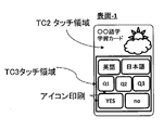
- this card has a touch area TC2 and a touch area TC3.
- the touch area TC2 for example, a title and a picture of “XX language learning card” are described, and five elements 111 (conductors) are provided on the back surface as shown in FIG. Therefore, the touch area TC2 is called a pattern code output touch area.
- labels such as “English”, “Japanese”, “Q1”, “Q2”, “Q3”, “YES”, “NO”, etc. are printed as icons on the touch area TC3. In this sense, the touch area TC3 is called an icon touch area.
- the touch area TC2 and the touch area TC3 are not electrically connected to each other.
- the conductor plate CA2 exists below the touch region TC2, but the conductor plate CA2 does not exist below the touch region TC3.
- the information device 200 reads the pattern code based on the arrangement of the element 111 (conductor) and identifies the type of card and the arrangement position of the element 111 (conductor). As a result, the information device 200 associates the touch area TC2 with the coordinate position on the touch panel of the information device 200. That is, the information device 200 specifies the position of the icon (“English” “Q1”) printed on the card on the touch panel.
- FIG. 12 is a cross-sectional view (hereinafter referred to as cross-section C) in which the card is cut along a plane perpendicular to the paper surface through the line connecting the C1 arrow and C2 arrow in FIG.
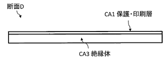
- FIG. 13 is a cross-sectional view (hereinafter referred to as cross-section D) in which the card is cut along a plane that passes through the line connecting the D1 arrow and D2 arrow in FIG.
- a cross section C in FIG. 12 has the same structure as the cross section A in FIG. 128.
- the conductor plate CA2 is not provided in the cross section D as shown in FIG. That is, there is no conductor plate CA2 immediately below the touch area TC3 in FIG.
- the touch panel detects an interaction due to a physical quantity (capacitance, electric field strength, etc.) via the element 111 (conductor) immediately below the touch area TC2. I can't.
- an insulator CA3 is provided in the section D.
- the insulator CA3 may be the same as the insulator around the element 111 (conductor) in the section C. Since the insulator CA3 has a certain dielectric constant, when the user touches the surface of the protective / printing layer CA1, the touch panel detects an interaction due to a physical quantity such as capacitance and electric field strength, and specifies the touch position. .
- the protective / printing layer CA1 and the insulator CA3 are made of a transparent material, the user can view the screen and operate the touch panel from above the card even when the user places the card on the touch panel.
- the protective / printing layer CA1 and the insulator CA3 may be a transparent medium such as glass or acrylic.
- the protective / printing layer CA1 and the insulator CA3 may be integrated with each other regardless of whether they are transparent or non-transparent.
- FIG. 14 is a modified example of a cross-sectional view (hereinafter referred to as a cross-section CC) in which a card is cut along a plane perpendicular to the paper plane passing through a line connecting the arrows C1 and C2 in FIG.
- both the element 111 (conductor) and the conductor plate CA2 may be formed by printing to form the element 111A and the conductive plate 111A.
- both the element 111A and the conductive plate 111A can be said to be printed thin films.
- the element 111A and the conductive plate 111A may be connected by a conductive line.
- portions other than the element 111A, the conductive plate 111A, and the conductive lines may be embedded with an insulator CA3 to form a card-type housing.
- a portion other than the element 111A, the conductive plate 111A, and the conductive line may be partially formed as a gap.
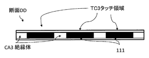
- FIG. 15 is a modified example of a cross-sectional view (hereinafter referred to as a cross-section DD) in which a card is cut along a plane perpendicular to the paper surface passing through the line connecting the D1 arrow and the D2 arrow in FIG.
- an element 111 (conductor) is provided under each icon printed in the touch area TC3.
- the icon illustrated in FIG. 11 label such as “English”
- physical quantities such as electrostatic capacitance and electric field strength by the finger interact with the touch panel via the element 111 (conductor) immediately below. Therefore, the information device 200 can recognize which icon is pressed.
- the card may slide or rotate when the user touches the icon.
- the information device 200 cannot take the correspondence between the touch area and the touch position. Therefore, an anti-slip material may be applied to the back of the card so that the card does not slide or rotate.
- a predetermined icon can be selected without any problem without applying anti-slip material.
- FIG. 16 is an example of another card for games.
- the card is provided with a transparent touch area TC4.
- the transparent touch region TC4 may be a transparent dielectric such as glass or acrylic.
- the structure of the back surface of the touch area TC2 is the same as that in the case of FIGS. 10 and 11, and the element 111 (conductor) is arranged.
- an icon image displayed on the display of the information device 200 is displayed in the transparent touch area TC4.
- the smartphone screen is displayed diagonally according to the direction of the card so that it fits within the transparent frame. However, even if the card is rotated / moved, the card is displayed at the same position.
- the touch panel can detect the touch position of the finger and specify the touched position by the interaction of the finger with the touch panel. That is, the electrostatic capacitance by the finger or the electric field strength can be detected by the touch panel through the transparent dielectric in the transparent touch region TC4. Therefore, the application executed on the information device 200 may execute a process corresponding to the icon displayed at the touched position.
- the touch area TC2 and the transparent touch area TC4 are covered with a conductive transparent film and connected to the conductor plate CA2 illustrated in FIG. 12, the touch area is displayed while the user is touching the transparent touch area TC4. Sufficient interaction from the element 111 (conductor) on the back surface of the TC2 to the touch panel can be given, and the information device 200 can recognize the arrangement of the element 111 (conductor). In that case, the user can give an interaction with a finger to the touch panel of the icon portion on the display such as “English” via the transparent touch area TC4, and can select an icon on the display.
- FIG. 17 shows an example in which the drawing application process is executed on the card shown in FIG.
- the drawing application executed on the information device 200 can acquire the movement locus of the finger via the touch panel by the interaction with the finger from the transparent touch area TC4.
- the drawing application may draw a line on the display according to the trajectory. Therefore, for example, the user can draw a character in the drawing area of the drawing application immediately below the transparent touch area TC4 of the card placed on the touch panel of the information device 200.
- FIG. 18 is a processing example of a game program that the information device 200 recognizes and executes the cards illustrated in FIGS. 3 to 17.
- the central processing unit (CPU) of the information device 200 starts a game program according to a user operation. For example, first, a character appears in a game scene (S1). Then, the CPU waits for the card to be placed on the touch panel (S2). When the CPU detects that the card is placed on the touch panel (YES in S2), the CPU specifies the type of the card from the arrangement of the elements 111 and specifies the relative position (arrangement) of the card on the touch panel. Then, the CPU waits for the user's finger to touch the card icon. When the card has the transparent touch area TC4, the CPU waits for the user's finger to touch the icon on the display (S4).
- the CPU detects a finger touch (YES in S4), it is determined whether or not the touched icon is an instruction to end the game program (S5). If the touched icon does not instruct the end of the game program, the CPU causes the character to execute an action corresponding to the touch position. Then, the CPU returns the process to S4. On the other hand, if it is determined in S5 that the touched icon is an instruction to end the game program, the CPU ends the game program.
- a game card or other item can be formed with a simple configuration using the insulator, the element 111, the conductor plate CA2, and the like.
- a card or an article is played by using a smaller number (for example, four) of elements 111 than the number of touched positions (for example, five) that can be detected simultaneously by the touch panel.
- a touch panel such as an information device or an information device 200, a touch operation with a finger is possible.
- Embodiment 2 shows an example of the arrangement of fixed pattern codes, unlike the example of pattern codes in which the output of the conductor is electrically variable and output.
- the pattern code of this embodiment is characterized in that two types of conductors, a reference conductor and an information conductor, are provided, and the pattern code direction and the pattern code are defined by the positional relationship between the reference conductor and the information conductor.
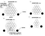
- FIGS. 19A and 19B are diagrams for explaining a case where three to four conductors having the same size are arranged.
- FIG. 19A shows a case where the distance between the reference conductors is 43 mm
- FIG. 19B shows a case where the distance between the reference conductors is 38 mm.
- C is a figure shown when the distance between standard conductors is 33 mm
- (d) is a figure showing the case where the distance between standard conductors is 28 mm.
- the direction of the pattern code is determined, and a unique pattern code can be defined.
- the distance between the two reference conductors is greater than the distance between any other conductors (between the reference conductor and the information conductor, between the information conductor and the information conductor), that is, between any conductors.
- the two reference conductors are arranged so that the distance between the two reference conductors becomes the maximum value. Thus, if two conductors having the maximum distance between the conductors are searched, it can be understood that the two are reference conductors. Then, it can be seen that the remaining one or two are information conductors, the direction of the pattern code is determined from the positional relationship between the reference conductor and the information conductor, and a unique pattern code can be defined.
- distance between conductors is the distance from the center of one conductor to the center of another conductor.
- the distance between the conductors is preferably about 10 mm. However, the preferred distance varies depending on the performance of the smartphone or tablet.
- (A) is a diagram showing a case where the distance between the reference conductors is 43 mm.
- placement candidates are information conductor placement candidates (hereinafter “placement candidates”). Arrangement candidates are at intervals of 5 mm. If the recognition error is small, it is possible to increase the number of information conductors that can be arranged by shortening the interval between the arrangement candidates and define a large number of pattern codes. In addition, when arrange
- the distance between the reference conductors is 43 mm
- Conductors cannot be placed so that the distance between conductors is less than 10 mm. This is because there is a possibility that the adjacent two cannot be recognized. Therefore, combinations that are less than 10 mm are excluded.
- (B) is a diagram showing a case where the distance between the reference conductors is 38 mm.
- (C) is a diagram showing a case where the distance between the reference conductors is 33 mm.
- the distance between the conductors is 4 mm or more shorter than the distance between the reference conductors (that is, the distance between the conductors is 29 mm or less).
- (D) is a diagram showing a case where the distance between the reference conductors is 28 mm.
- the distance between the reference conductors is not limited to the above four types, and the reference conductors may be arranged anywhere as long as the direction of the pattern code can be recognized. Even if the reference conductor is not arranged, the pattern code may be defined by forming a unique arrangement using only the information conductor. A unique arrangement is an arrangement in which the same pattern does not exist even when rotated and moved.
- FIG. 20 is a diagram for explaining a case where a reference medium having a size different from that of the information conductor is arranged, and a total of 3 to 4 conductors are arranged.
- A When the distance between the reference conductors is 35 mm, (b) When the distance between the reference conductors is 30 mm, (c) When the distance between the reference conductors is 25 mm, (d) When the distance between the reference conductors is 20 mm It is a figure shown about a case.
- the direction of the pattern code is determined, and a unique pattern code can be defined.
- the two reference conductors are made different in size from the information conductors so that the information device 200 having a touch panel can recognize them (in the figure, the reference conductors are made larger than the information conductors). Thereby, the information device 200 recognizes the size of the conductor and knows that the larger conductor is the reference conductor. Then, it can be seen that the remaining one or two are information conductors, and the direction of the pattern code is determined from the positional relationship between the reference conductor and the information conductor.
- the distance between conductors (the distance from the center of one conductor to the center of another conductor) is preferably about 10 mm. However, the preferred distance varies depending on the performance of the smartphone or tablet.
- (A) is a diagram showing a case where the distance between the reference conductors is 35 mm.
- Placement candidates are at intervals of 5 mm. If the recognition error is small, the number of information conductors that can be arranged can be increased by shortening the interval between the arrangement candidates, and a large number of pattern codes can be defined. In the actual arrangement, the distances of 10 mm or more are arranged so that two adjacent conductors can be reliably recognized.
- Conductors cannot be placed so that the distance between conductors is less than 10 mm. This is because there is a possibility that the adjacent two cannot be recognized. Therefore, combinations that are less than 10 mm are excluded.
- (B) is a diagram showing a case where the distance between the reference conductors is 30 mm.
- (C) is a diagram showing a case where the distance between the reference conductors is 25 mm.
- (D) is a diagram showing a case where the distance between the reference conductors is 20 mm.
- the distance between the reference conductors is not limited to the above four types, and the reference conductors may be arranged anywhere as long as the direction of the pattern code can be recognized. Further, by changing the sizes of the two reference conductors, the direction of the pattern code can be recognized regardless of where the information conductors are arranged.
- each pattern code, device, and the like of each embodiment can be used in appropriate combination beyond the embodiment.
- a pattern code used in a stamp type code generator can be used in a card type device, and an information reading device used in a card type can be used in a stamp type device.
- the reverse is also possible.
- Embodiment 34 illustrates the configuration of a card-type device that does not include an active circuit driven by a power source such as a semiconductor switch.
- the device 110Y1 has a structure in which two dielectric layers are bonded together.
- an action surface that acts on the information device 200 (for example, a surface that is brought into contact with the touch panel) is referred to as a back surface.
- the front surface the surface operated by the user is referred to as the front surface. The surface can be said to be the opposite surface of the working surface.
- the dielectric layer including the surface that serves as the working surface (that is, the back surface) of the card-type device is referred to as a lower layer.
- the dielectric layer including the surface to be the surface of the card type device is referred to as an upper layer.
- the surfaces to be bonded to each other are called bonding surfaces.
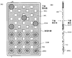
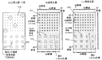
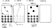
- FIG. 21A illustrates the configuration of the upper layer surface of the device 110Y1.
- FIG. 21B is a combination of the partial cross-sectional views of FIG. That is, the upper side toward the paper surface in FIG. 21B is a cross section of the device 110Y1 taken along the arrow A1 in FIG. 21A, and the lower side toward the paper surface in FIG. It is the cross section which cut
- the boundary between the two cross sections is indicated by two wavy lines.
- the wiring layer WR1 is formed in a lattice pattern on the substrate surface (upper surface) of the dielectric layer.
- the wiring layer WR1 has a configuration in which wirings of metals, for example, copper, aluminum, and the like are combined in a vertical and horizontal combination.
- the interval between the wiring layers WR1 is an interval at which the user can touch the wiring layer WR1 when the user's finger touches the upper layer surface.
- the apparatus 110Y1 used by an adult user is set to, for example, about several millimeters. Is done.
- the wiring layer WR1 can be said to be a wiring layer formed on the opposite side of the dielectric layer.
- through holes TH1 are formed at the intersections of the wirings in the upper region (referred to as the first region) toward the paper surface.
- the through hole TH1 is plated with a conductive metal or is filled with a conductive metal. Therefore, the metal in the through hole TH1 electrically connects the surface of the upper dielectric layer and the bonding surface.
- the through hole TH1 is provided with a metal contact ATP1 on the upper layer bonding surface, that is, the back surface side of FIG.
- the metal contact ATP1 is used to connect the upper layer through hole TH1 to a lower layer conductor, for example, a through hole, when the upper conductive layer and the lower conductive layer are joined.
- contact terminals 114A are formed between the wirings in the lower region (referred to as the second region) toward the paper surface.
- the contact terminal 114A has a thin metal plate structure.
- the dimension of the contact terminal 114A in plan view is a dimension that does not contact the wiring of the wiring layer WR1.
- the contact terminal 114A is electrically connected to the contact ATP1 on the joint surface side through a metal plated or embedded in the through hole TH1.
- first region and the “second region” are defined on the surface of the upper dielectric layer.
- first region and the “second region” are defined on the bonding surface of the upper dielectric layer.
- first region and “second region” can be defined as regions corresponding to “first region” and “second region” of the upper dielectric layer.
- the corresponding region here means that when the upper dielectric layer and the lower dielectric layer are joined, the “first region” and “second region” of the upper dielectric layer are perpendicular to the upper surface (that is, in the plan view direction). It can be said that the area is projected onto the lower layer.
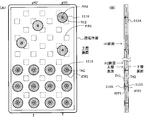
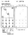
- FIG. 22A illustrates the configuration of the bonding surface before the element 111 is formed on the dielectric layer below the device 110Y1.
- FIG. 22B is a cross-sectional view of the device 110Y1 in FIG.
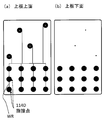
- FIG. 23A illustrates the structure of the bonding surface after the element 111 is formed on the lower dielectric layer of the device 110Y1.
- FIG. 23B is a cross-sectional view of the device 110Y1 of FIG.
- a frame portion is formed around the lower joint surface, and a plurality of protrusions PIR1 are formed on the joint surface surrounded by the frame portion. .
- the frame and the plurality of protrusions PIR1 act as spacers that form a gap SPC between the upper layer and the lower layer when the upper layer and the lower layer of the dielectric layer are joined.
- the protrusion PIR1 is formed on the lower joint surface corresponding to the wiring layer WR1 on the upper surface. Accordingly, the gap SPC formed between the upper layer and the lower layer by the frame portion and the plurality of protrusions PIR1 is formed in a portion including the portion immediately below the wiring layer WR1 on the upper layer surface.
- a plurality of protrusions PR2 and a through hole TH2 that penetrates the protrusion PR2 from the bonding surface side to the lower layer back surface side are formed in a region where the bonding surface of the upper second region is bonded.
- the through hole TH2 is plated or filled with a conductive metal to ensure conductivity between the joint surface side and the lower layer back surface side.
- a contact ATP2 for making electrical contact with the upper contact ATP1 is formed on the joint surface side of the through hole TH2.
- FIG. 23A and FIG. 23B illustrate a configuration in which the element 111A is formed in the lower dielectric layer in FIG. 22A and FIG. 22B.
- the element 111A is formed by inserting or filling a metal into a hole formed by hollowing out a lower dielectric layer. Therefore, when the upper and lower dielectric layers are joined, the element 111A contacts one of the contacts ATP1 on the upper joint surface and is connected to the wiring layer WR1 on the upper surface by the metal in the through hole TH1. Therefore, the lower dielectric layer element 111A is formed in the lower region corresponding to the first region where the metal of the through hole TH1 is connected to the wiring of the upper wiring layer WR1. By making the interval between the through holes TH1 smaller than the dimension of the element 111Al, the element 111Al is connected to the through hole TH1 regardless of the position of the lower layer corresponding to the first region.
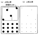
- FIG. 24A illustrates the configuration of the working surface acting on the back surface (lower layer back surface) of the device 110Y1, that is, the touch panel of the information device 200.
- the protrusion PIR1 is virtually illustrated by a dotted line for reference. Therefore, the gap SPC is formed inside the dielectric between the protrusions PIR1.
- FIG. 24B illustrates an outline of a cross section of the device 110Y1 after bonding the upper and lower dielectric layers.
- a plurality of elements 111A are formed in the region on the back surface corresponding to the first region in the upper layer of the device 110Y1.
- the element 111A is connected to the wiring layer WR1 through the upper layer contact ATP1 and the through hole TH1 (see FIGS. 21A and 21B).
- the contact ATP1 and the through hole TH1 can be said to be an example of a first through conductive path that connects one or more elements formed in the first region and the wiring layer through the dielectric layer.
- the information device 200 detects the arrangement positions of the plurality of elements 111A and specifies information corresponding to the shape of the arrangement positions. In this sense, it can be said that the plurality of elements 111A define a fixed arrangement pattern.
- the one or more elements formed in the first region form a physical quantity that can be detected by the sensor when the user's finger contacts the wiring layer, and when the user's finger does not contact the wiring layer, It can be said that a physical quantity that can be detected by the sensor is not formed.
- the information device 200 can be used even when the device 110Y1 is in contact with or close to the touch panel of the information device 200 in a state where the user's finger is not in contact with the wiring layer WR1. It is possible to detect the arrangement positions of the plurality of elements 111A and specify information corresponding to the shape of the arrangement positions. This is because the capacitance formed by the wiring layer WR1 and the plurality of elements 111A is sufficiently large so that the touch panel of the information device 200 can be recognized as a touch operation.
- the element 111A is an example of one or more elements formed in the first region of the working surface.
- a plurality of elements 111B are formed in the back region corresponding to the second region in the upper layer of the device 110Y1.
- the plurality of elements 111B can be formed by printing with a conductive material, for example, conductive ink.
- Each of the plurality of elements 111B is electrically connected to each of the contact terminals 114A on the surface through the through hole TH2 on the lower layer side, the contact ATP2, the contact ATP1 on the upper layer side, and the through hole TH1. Therefore, when the user's finger comes into contact with the contact terminal 114A on the front surface, the user and the element 111B are electrically connected, and the capacitance or electric field is applied to the touch panel of the information device 200 that is in contact with or close to the back surface of the device 110Y1. Causes a change in intensity.
- the touch operation is sequentially performed at the position of the element 111B of the touch panel of the information device 200 in accordance with the operation by the user's finger. Can be executed. Therefore, the contact terminal 114A arranged in the second region on the surface functions as an input device similar to a keyboard or a touch pad. For example, by forming an icon on each of the contact terminals 114A with a conductive material, and executing an application program that recognizes the arrangement of the information apparatus 200 icon, the information apparatus can be transferred from the user to the contact terminal 114A. Information associated with the operation can be acquired.
- the element 111B is an example of one or more elements formed in the second region of the working surface.
- the lower through hole TH2, the contact ATP2, the upper contact ATP1, and the through hole TH1 pass through the dielectric layer and connect one or more elements formed in the second region to the contact terminal. It can be said that it is an example of two through conductive paths.
- the wiring layer WR1 is formed by wiring arranged at a sufficiently smaller interval than the width of the user's finger, when the user operates the contact terminal 114A, the user's finger Will touch the wiring layer WR1. Therefore, information input to the information device 200 in the fixed arrangement pattern and information input from the contact terminal 114A as an input device are executed at the same timing. Therefore, for example, the information device 200 can recognize a specific identifier by the fixed arrangement pattern, execute a process according to the identifier, and receive an input corresponding to the process from the user. Accordingly, in the device 110Y1, the wiring layer is arranged at a wiring interval that allows the finger to contact any of the wirings when the user's finger contacts the opposite surface of the card shape with respect to the second region. Can do.
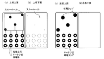
- FIG. 25 to FIG. 27 illustrate the configuration of the device 110Y2 as another example of the embodiment 33. Since the structure of the upper layer of the dielectric layer of the device 110Y2 is the same as that of the device 110Y1 (FIGS. 21A and 21B), description thereof is omitted.
- FIG. 25A illustrates a plan view of the bonding surface under the dielectric layer of the device 110Y2.
- FIG. 25B is a diagram in which the D1 sectional view and the D2 sectional view of FIG. 25A are combined and virtually connected by two wavy lines. As shown in the figure, a plurality of protrusions PIR2 are formed in a lattice pattern in a lower layer region corresponding to the first upper region.
- Each projection PIR2 is formed with a through hole TH2 penetrating the joint surface side and the back surface.
- the through hole TH2 is plated or filled with metal, and electrically connects the joint surface side and the back surface.
- a contact ATP3 is formed on the joint surface side of the through hole TH2. Therefore, when the upper and lower dielectric layers are joined, the lower through hole TH2 is connected to the surface wiring layer WR1 via the contact ATP3, the upper contact ATP1, and the through hole TH1. Since the structure of the lower layer area corresponding to the upper second area of the device 110Y2 is the same as that of the device 110Y1, the same reference numerals are given and the description thereof is omitted.
- FIGS. 26A and 26B illustrate a state in which the element 111C is formed on the lower dielectric back surface in FIGS. 25A and 25B.
- the element 111A of the device 110Y1 was formed by hollowing out a lower layer of a dielectric material and fitting or filling a metal.
- the element 111A is formed by printing with a conductive material, for example, conductive ink. Under the dielectric, a through hole TH2 plated with metal or filled with a contact ATP3 is formed. Therefore, when the upper and lower dielectric layers are joined, the element 111A is connected to the wiring layer WR1 on the surface via the upper contact ATP1 and the through hole TH1.
- FIG. 27A illustrates the configuration of the working surface acting on the back surface (lower layer back surface) of the device 110Y2, that is, the touch panel of the information device 200.
- the protrusion PIR2 and the through hole TH2 are virtually illustrated by dotted lines for reference. Therefore, a gap SPC is formed inside the dielectric between the protrusions PIR2.
- FIG. 27B illustrates an outline of a cross section of the device 110Y2 after bonding the upper and lower dielectric layers.
- the printed element 111C is connected to the wiring layer WR1 on the surface through the lower through hole TH2, the contact ATP3, the upper contact ATP1, and the through hole TH1.
- the device 110Y2 can be operated in the same manner as the device 110Y1.
- the element 111C is formed by printing, various arrangement patterns of the plurality of elements 111C can be formed flexibly. Therefore, according to the apparatus 110Y2, it becomes easy to cope with various application programs executed by the information device 200, and it is possible to cope with mass production of the apparatus 110Y2.
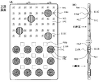
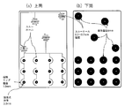
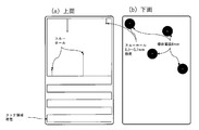
- FIG. 28A illustrates the structure of the upper surface of the device 110Y3.
- FIG. 28B is a combination of the partial cross-sectional views of FIG. That is, the upper side toward the paper surface in FIG. 28B is a cross section of the device 110Y3 taken along the E1 arrow in FIG. 28A, and the lower side toward the paper surface in FIG. It is the cross section which cut
- FIG. 28B the boundary between the two cross sections is shown divided by two wavy lines.
- the configuration of the upper surface of the dielectric layer of the device 110Y3 is the same as that of the devices 110Y1 and 110Y2.
- a plurality of protrusions PIR4, PIR5, and protrusions PIR6 are formed on the upper joint surface of the dielectric layer of the device 110Y3. Is different.
- the protrusion PIR4 is formed on the bonding surface side at a position corresponding to the position of the through hole TH1 connected to the wiring layer WR1 in the upper first region. Therefore, a through hole TH1 that penetrates the upper dielectric layer and is connected to the wiring layer WR1 is formed in the protrusion PIR4.
- the protrusion PIR4 is formed on the joint surface side at a position corresponding to the position of the through hole TH1 connected to the contact terminal 114A in the second region of the upper layer. Therefore, a through hole TH1 that penetrates the upper dielectric layer and is connected to the contact terminal 114A is formed in the protrusion PIR5.
- the protrusion PIR6 is a region where the density of the protrusions PIR4 and PIR5 is low, and acts as a spacer for forming a gap between the upper layer and the lower layer to be joined.
- FIG. 29A is a plan view illustrating the bonding surface of the lower layer of the dielectric layer of the device 110Y3.
- FIG. 29B is a diagram in which the F1 cross-sectional view and the F2 cross-sectional view of FIG. 29A are combined and virtually connected by two wavy lines.
- the lower layer of the dielectric layer of the device 110Y3 is formed by forming a hole in a flat dielectric layer without unevenness. That is, as shown in FIG. 28 (B), a plurality of projections PIR4, projections PIR5, and projections PIR6 are formed on the upper-layer joint surface.
- the lower layer of the dielectric layer of the device 110Y3 can be configured as a flat plate.
- a plurality of holes HL1 and HL2 are formed in the lower layer of the dielectric layer of the device 110Y3.
- the hole HL1 formed in the lower layer region corresponding to the upper first region is for penetrating the protrusion PIR4 of the upper layer bonding surface at the time of bonding.
- the hole HL2 formed in the lower layer region corresponding to the upper second region is for penetrating the protrusion PIR5 of the upper layer bonding surface at the time of bonding.
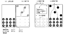
- FIG. 30A illustrates the configuration of the back surface of the device 110Y3 after joining the upper layer and the lower layer (the lower surface of the lower layer), that is, the working surface acting on the touch panel of the information device 200.
- FIG. 30B illustrates an outline of a cross section of the device 110Y3 after bonding the upper and lower dielectrics.
- the protrusions PIR4 to PIR6 and the through hole TH1 are virtually illustrated by dotted lines for reference. That is, the protrusion PIR4 penetrates the hole HL1 at a position corresponding to the first region of the upper layer.
- the through hole TH1 in the protrusion PIR4 electrically connects the front surface and the back surface of the device 110Y3. Therefore, the element 111C printed and molded on the back surface is connected to the wiring layer WR1 on the front surface through the through hole TH1 in the protrusion PIR4.
- the protrusion PIR5 penetrates the hole HL2 at a position corresponding to the second region of the upper layer.
- the through hole TH1 in the protrusion PIR5 electrically connects the front surface and the back surface of the device 110Y3. Therefore, the element 111B printed and molded on the back surface is connected to the contact terminal 114A on the front surface through the through hole TH1 in the protrusion PIR4.
- the lower layer has a very simple flat plate configuration, and can be configured more suitable for printing.
- the device 110Y4 will be described with reference to FIGS.
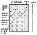
- the wiring layer WR1 is laid on almost the entire upper surface of the upper layer of the dielectric layer with a stitch, lattice shape, or other configuration. With such a configuration, the surface area due to the wiring layer WR1 is increased, and the capacitance due to the wiring layer WR1 and the elements 111A and 111C can be increased.
- the touch panel can detect the contact or proximity of the device 110Y.
- the touch panel of the information device 200 has the wiring layer WR1 and the element 111A, In an application based on the assumption that the capacitance due to 111C is not detected, erroneous detection may occur. Therefore, hereinafter, a configuration that reduces the capacitance caused by the wiring layer WR1 and the elements 111A and 111C as much as possible is exemplified by the device 110Y4.
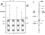
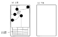
- FIG. 31A illustrates the configuration of the upper layer surface of the device 110Y4.
- FIG. 31B is a combination of the partial cross-sectional views of FIG. That is, the upper side toward the paper surface in FIG. 31B is a cross section obtained by cutting the device 110Y4 along the G1 arrow in FIG. 31A, and the lower side toward the paper surface in FIG. It is the cross section which cut
- the boundary between the two cross sections is indicated by two wavy lines.
- the configuration of the contact conductor 114A, the through hole TH1 connected to the contact conductor 114A, and the contact ATP1 in the cross-sectional configuration of the device 110Y4 is the same as that of the device 110Y1.
- the wiring layer WR3 is formed on the bonding surface side in the upper first region. Therefore, in FIG. 31A, the wiring layer WR3 is indicated by a dotted line.
- a contact ATP5 is formed on the bonding surface side of the wiring layer WR3.
- the contact ATP is a contact for electrically connecting to the contact ATP3 on the lower surface when the upper layer and the lower layer are bonded.
- the wiring layer WR3 is formed on the bonding surface side, thereby reducing the possibility that a fixed arrangement pattern is erroneously input to the information device when the user contacts a portion other than the wiring layer WR2 in the second region. it can.
- the wiring layer WR3 may be formed on the surface in an application in which the user does not touch the information device with a fixed arrangement pattern due to contact with a portion other than the wiring layer WR2 in the second region. Good.
- the wiring layer WR2 is formed in a one-dimensional line and space configuration instead of a stitch shape, and is connected to one wiring at one end of each wiring.
- the wiring layer WR3 is also formed in a one-dimensional line and space configuration on the bonding surface side, and is connected to the surface wiring layer WR2 through the through hole TH5.
- FIG. 32A illustrates the configuration of the lower joint surface of the device 110Y4.
- FIG. 32B is a combination of the partial cross-sectional views of FIG. That is, the upper side toward the paper surface in FIG. 32B is a cross section obtained by cutting the device 110Y4 along the arrow H1 in FIG. 32A, and the lower side toward the paper surface in FIG. It is the cross section which cut
- FIG. 33A is a plan view illustrating the configuration of the back surface of the device 110Y4 in which the upper layer and the lower layer are joined, and FIG. 33B shows an outline of the cross-sectional configuration of the device 110Y4 in which the upper layer and the lower layer are joined.
- FIG. 33A is a plan view illustrating the configuration of the back surface of the device 110Y4 in which the upper layer and the lower layer are joined
- FIG. 33B shows an outline of the cross-
- a through hole TH2 is formed in the projecting portion PIR3 on the lower joint surface as in the device 110Y1, and is connected to the element 111C on the back surface side.
- a contact ATP3 is formed on the joint surface side of the through hole TH2. Therefore, the device 110Y4 is different from the device 110Y1 in that the protrusion PIR3, the through hole TH2, and the contact ATP3 are formed only in the portion corresponding to the element 111C.
- the configuration of the portion connecting the front surface and the back surface of the device 110Y4 is the same as that of the device 110Y1.
- the line and space configuration on the straight line of the wiring layer WR2 with which the user's finger comes into contact is set, and the wiring layer WR3 for connecting to the element 111C on the back surface of the device 110Y4 is used as the first lead wire.
- the capacitance of the wiring layers WR2 and WR3 can be reduced.
- the touch panel of the information device 200 can recognize a so-called fixed arrangement pattern by the element 111C when the user's finger contacts the wiring layer WR2.
- information input by the contact terminal 114A in the device 110Y4 is the same as that in the devices 110Y1 to 110Y3.
- FIG. 34 illustrates the configuration of the back surface of the device 110Y5.
- the protrusion PIR1 that supports the air gap SPC inside the dielectric layer in which the upper layer and the lower layer are joined is virtually illustrated by a dotted line.
- the contact terminals 114A on the surface of the device 110Y5 and the wiring layer WR10 are virtually illustrated by dotted lines.
- the contact terminal 114A is formed by printing with a conductive material, for example.
- the element 111C is printed on the back surface, and connected to the wiring layer WR10 on the front surface similarly to the devices 110Y1 to 110Y4 through the through holes TH2.
- the wiring layer WR10 is not configured to be spread over a wide range like a mesh, a lattice, or a line and space pattern, and the element 110B and the contact terminal 114A are as short as possible. It is an arrangement that can be connected with.
- a plurality of elements 111B that input information to the information device 200 in a fixed arrangement pattern are formed in three groups connected to the contact terminals 114A1, 114A2, and 114A3.
- the wiring length of the wiring layer WR10 of each group is sufficiently short, and the touch panel of the information device 200 is connected to the working surface (back surface) of the information device 200 only by the capacitance between the wiring layer WR10 of each group and the element 111B.
- Contact or proximity cannot be detected.
- the capacitance between the wiring layer WR10 and the element 111B in each group can be adjusted so that the arrangement pattern of the element 111B is detected only when the user's finger contacts the wiring layer WR10 in each group. .
- the user can cause the information device 200 to detect the combination of the arrangement patterns by operating in the desired order of each group.
- six types of input are possible depending on the order in which the user touches the contact terminals 114A1, 114A2, and 114A3 with a finger. Therefore, by preparing a plurality of devices 110Y5 having different arrangement patterns of the plurality of elements 111B, various applications can be provided to the user.
- the dotted circle is a contact terminal 114A formed on the surface as a touch area.
- the wiring (conductive wire) included in the wiring layer WR10 may be extended through the center of the dotted circle and further to the end of the dotted circle to be a conductive wire for touch.
- a plurality of combinations of one or more elements formed in the first region and the wiring layer connected to the one or more elements are formed in the device 110Y5.
- the user sequentially touches the contact terminals 114A1, 114A2, and 114A3 corresponding to each group with a finger, the user sequentially touches each wiring layer included in the plurality of sets to be included in the plurality of sets. It can be said that information accompanying a change in physical quantity from one or more elements formed in the first region is input to the panel.
- FIG. 35 illustrates the configuration of the back surface of the device 110Y6.
- the device 110Y6 is provided with an information input unit by an element 111B. Therefore, according to the device 110Y6, the user can input a combination of fixed information to the information device 200 by a combination of fixed arrangement patterns by the contact terminals 114A1 and 114A2, and can use general-purpose alphanumeric characters and special characters. Key input such as symbols, selection with dedicated keys, cursor operation, etc. are possible.
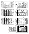
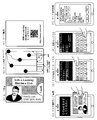
- [application] 36 to 39 recognize a conductive pattern arranged on a card, and touch a plurality of touch areas printed as icons (may be part of the graphic) on the card surface. In this embodiment, data input and application activation / operation are performed.
- FIG. 36 shows examples of various member cards.
- the facility arrangement pattern, membership type, etc. can be identified by the conductor arrangement pattern.
- you touch the number icon for the password and touch the ENTER icon you can enter the password and authenticate yourself. Cancel the password input. If the password is incorrect, touch the CANCEL icon and enter it again.
- you can authenticate yourself you can browse and enjoy various information and services of the facility.
- the card surface and the password is printed, the card is provided to the user for sales promotion etc., the web is accessed, the card is placed in a predetermined area, and the password obtained by scratch is entered If so, privileges and special information / content can be provided.
- FIG. 37 shows an example of a sightseeing card. If a tourist card is put on the touch panel and a language icon is touched, explanations of sightseeing spots and event information can be viewed in that language.
- Cards and touch panels may be installed at hotels, facilities, tourist information centers, etc. for inbound travel.
- a travel agent, a transportation facility, or the like may install and distribute the card so that it can be viewed on the user's smartphone.
- product descriptions and colors Information such as variations and prices can be acquired.
- the display may display the information by displaying frames of performance, color variations, etc., and hovering over the area. Even if a product is out of stock, information may be provided or ordered by displaying a product card.
- advertisement cards printed with eye-catching designs and photographs may be displayed at various locations and provided to users so that content with advertisements can be acquired.
- FIG. 38 shows an example of a “science learning card” for education.
- the problem comes out when you put the learning card on the tablet and touch the question icon. If the answer is 4 choices, touch a number from 1 to 4. If it is correct, touch XX. If the answer is correct, a correct or incorrect result may be output on the spot such as ping pong. In addition, when an answer icon is touched, an answer or an explanation of the answer may be given. Further, when the question icon is touched, the next question is output. If you touch the scoring icon, the scoring result of the answer after deceiving the card (3 out of 5 questions is correct) will be output. When the end icon is touched, the progress of the question is cleared, and when the question icon is touched again, the process starts from the first question.
- FIG. 39 shows an example of a game card.
- the character of that card is displayed. Touching the arrow icon moves the character in that direction. Touch the STOP icon to stop moving. Touch the JUMP icon to jump the character. Touch the GET icon to get an item. Touch the ATTACK icon to attack the opponent. The attack direction is changed by turning the card to attack the direction.
- MAP is displayed on the display, the game can be advanced while moving the card to a predetermined position.
- the conductor has a single size and shape, and so many patterns cannot be defined.
- the current touch panel can recognize the touch area and the maximum touch width, a considerable number of patterns can be defined as shown in FIG. 40 by changing the size of each pattern.
- the touch shape can be recognized in the future, and it becomes possible to define and recognize more conductor patterns by changing the shape.
- FIG. 40 shows an embodiment in which the size of the conductor is changed.
- Fig. A shows that the size of each conductor can be set and recognized, and the distance between conductor A and conductor B is the longest when three and four conductors whose orientation can be recognized are used. The two are considered as reference conductors.
- the card that is not controlled by the electric circuit has been discussed above. However, it is possible to change the size and shape of the conductor that reacts electrically. Similarly, the conductor pattern can be changed in the size and shape of the conductor. It goes without saying that more information can be defined and recognized.
- the position recognition method of the element 111 by the information device 200 and the processing of the program according to this position recognition method are illustrated.
- the device 110 has the same configuration as the device 110Y of the thirty-fourth embodiment, for example. Therefore, the target on which the information device 200 performs position recognition in the present embodiment is, for example, a thin plate-like device without a power source.
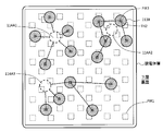
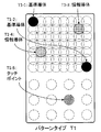
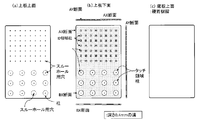
- FIG. 41 is an arrangement example (referred to as type 1) of the elements 111 on the working surface of the device 110 that is the processing target of the information device 200 of the present embodiment
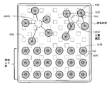
- FIG. FIG. 43 is a diagram for explaining an ID area and a touch area in which the element 111 on the working surface of the device 110 is arranged.
- the device 110 includes elements 111 on virtual lattice points that are virtually formed on a working surface that is close to or in contact with the touch panel of the information device 200. Be placed. That is, the element 111 is arranged so that the center of the element 111 is positioned at each lattice point.
- the grid points include grid points in the ID area and grid points in the touch area.
- the reference conductor refers to an element 111 serving as a reference for determining a lattice position among the elements 111 arranged at lattice points in the ID region.
- the reference conductor is usually arranged at two four corners at diagonal positions in the rectangular ID region. That is, the arrangement positions of the reference conductors are limited to two types, one set of the upper left corner and the lower right corner (hereinafter referred to as pattern type 1) and one set of the upper right corner and the lower left corner (hereinafter referred to as pattern type 2). .
- the information conductor is an element 111 arranged at a lattice point of the ID area, and means an element 111 other than the reference conductor in the rectangular ID area.
- the touch area is an area that causes a physical quantity change to the touch panel on the action surface directly below (back side) of the finger contact when the user touches the finger contact provided on the opposite surface of the action surface of the device 110. It is.
- the contact terminal 114A of the above-described embodiment 34 can be exemplified.
- the position on the working surface that causes a physical quantity change on the surface of the touch panel by a finger contact on the upper surface (opposite surface of the working surface) of the device 110 and a touch operation on the finger contact ( The back surface position of the finger contact) is collectively referred to as a touch point.
- 3 ⁇ 4 12 touch points are provided.
- the number of touch points is not limited to 12.
- Elements 111 corresponding to the number of touch points may be provided at positions on the working surface corresponding to the touch points (positions at which physical quantity changes due to touch operations).
- the element 111 on the working surface corresponding to the touch point and the touch point may be connected by a conductor (conductive path), for example.
- the element 111 and the conductor may not be provided at the touch point and the position on the action surface corresponding to the touch point.
- the element 111 and the conductor may not be provided at the touch point and the position on the action surface corresponding to the touch point.
- the element 111 and the conductor may not be provided, when the user touches the touch point, on the working surface corresponding to the touch point according to the dielectric constant of the substrate on the thin plate of the device 110 ( A physical quantity change acting on the touch panel occurs on the back surface of the touch point.
- the dielectric constant of the substrate is sufficiently high, the touch panel of the information device 200 detects such a change in physical quantity even when there is no element 111 or a conductive path.
- the device 110 is a touch card having four elements 111 (two reference conductors and two information conductors) arranged in the ID area and 12 touch points in the touch area. It can be said. However, in the following, there may be a case where two reference conductors, two information conductors, and five touch points are combined, including the case where the element 111 is not in the touch area.
- FIG. 41 shows the pattern type 1 apparatus 110.
- FIG. 42 shows the pattern type 2 apparatus 110.
- the information conductors in the ID region are not arranged at two adjacent lattice points.
- the two information conductors are arranged (at the top, bottom, left, and right diagonally) with at least one candidate location indicated by a dotted line O (with at least one lattice point left).
- information conductors are exemplified by information conductors T1-3, T1-4, T2-3, and T2-4 with dot hatching.
- the reference conductor is exemplified by a black circle, and is exemplified by reference conductors T1-1, T1-2, T2-1, and T2-2.
- the two reference conductors are not limited to the four corners of the ID region, and may be arranged, for example, above and below the four corners or left and right. By making the positions of the two reference conductors other than the four corners, a large number of IDs for identifying the card can be set accordingly.
- ID area code A combination of an ID and a touch input 1 by a touch operation is called an ID area code.
- the ID area code recognition algorithm will be described with reference to FIGS.
- Step G1 The information device 200 recognizes five conductor detection positions by the touch panel and searches for two reference conductors from the five conductor detection positions.
- Step G2 The touch panel detects information conductors arranged at two information conductor arrangement positions (lattice points) of a predetermined number (for example, 48 places) of ID areas uniquely determined from two reference conductors. Recognize the defined ID.
- Step G3 Furthermore, the information device 200 specifies 12 touch areas uniquely determined from the two reference conductors.
- the information device 200 detects touch selection (one of twelve places) in the specified card ID by detecting a grid point on the touch area corresponding to the touch point on which the touch operation is performed, Recognize the touch operation related to the ID.
- the card-like device 110 is formed with a mark indicating a processing target.
- the information device 200 identifies a position on the device 110 that has been touched, and provides functions such as execution of an application corresponding to the mark attached to the identified position, and operation / viewing of content. Therefore, the user can execute the application, operate / view the content, and the like by touching a touch point near the mark indicating the selection target formed on the card-like device 110.
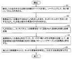
- the CPU of the information device 200 executes the process of FIG. 49 using a computer program that is executably expanded on the RAM.
- Step D1 The information device 200 detects the coordinate position where the physical quantity change at the element 111 in the ID region and the touch point occurs on the touch panel.
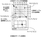
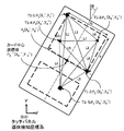
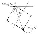
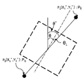
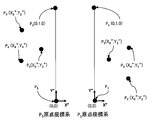
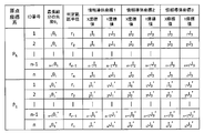
- the coordinate values of the detection points in the coordinate system on the touch panel in FIG. 45 are T1-1: P1 (X1 ′, Y1 ′), T1-2: P2 (X2 ′, Y2 ′), T1-3: P3 (X3 ′). , Y3 ′), T1-4: P4 (X4 ′, Y4 ′), T1-5: P5 (X5 ′, Y5 ′).
- the information device 200 calculates all the distances between two points out of a total of five points, that is, four points in the detected ID area and one point in the touch area.
- the information device 200 sorts as L1 to L10 from the longest distance between two points.
- the sorting result is obtained as L1> L2> L3> L4> L5> L6> L7> L8> L9> L10. Since the information device 200 detects L1 to L10 in the coordinate system on the touch panel, the numerical values of L1 to L10 acquired by the information device 200 are different from the actual size values.
- the XY coordinate system in FIG. 44 is a coordinate system on the working surface of the device 110 (card-like medium) with the lower left of the touch area as the origin. Also, the XiYi coordinate system of FIG. 44 is a coordinate value that is standardized so that the coordinate values can be collated with an ID search table (ID area coordinate value-ID number table of FIG.
- the coordinate value of each detection point when the card-shaped medium of FIG. 45 is placed on the touch panel by ⁇ rotation is represented by the X′Y ′ coordinate system of the touch panel. That is, the X′Y ′ coordinate system is a coordinate system of the touch panel when the card is placed on the touch panel by ⁇ rotation.
- the X "Y" coordinate system in FIG. 47 is a coordinate system in which a card placed by ⁇ rotation is rotated by ⁇ , the card orientation is positive (Y ”axis direction), and each point is coordinate-transformed. In these coordinate systems, the lower left is the origin, but the upper left (which may be the upper right or lower right) frequently used for coordinate detection of the touch panel may be the origin.
- the two reference conductors are included in the first to fifth ranges (L1 to L5) from the longest distance between the two points due to the geometric arrangement of the element 111.
- the reason why the two reference conductors are included in the range up to the fifth is that, as is clear from FIG. 44, the distance from at least one point of the touch area to the four points detected in the ID area is two pieces. This is because the distance may be longer than the distance between the reference conductors. If the card is arranged such that the distance from one point of the touch ID area farthest from T1-2 (X2, Y2) is shorter than the distance between the two reference conductors, the two reference conductors are It is included in the range from the longest distance between two points to the first to fourth.
- Step D2 the coordinates of both ends corresponding to the line segments of all the distances L1 to L5 from the first to the fifth are Pi and Pj.
- a rectangle can be generated by forming two triangles having apexes at right angles so that the actual size has a ratio of 42 mm to the actual card size of 36 mm.
- the information device 200 uses five detection points, for example, the center between two points regarded as the reference conductor as the center of the rotation angle (however, the information device 200 may use any position as the rotation center), ⁇
- the coordinates are converted so that the card can be rotated and placed in the positive direction (Y "axis direction).
- the ID area is within X1 ′′ to X2 ′′ and Y1 ′′ to Y2 ′′, and the conductor in the rectangular ID area can be easily recognized.
- the information device 200 geometrically moves the touch area downward. When there is one conductor in the touch area, the information device 200 can recognize two reference conductors, two information conductors, and one touch point.
- the information device 200 when determining whether or not there are conductors in the ID area and the touch area, the information device 200 considers the detection error of the element 111 (depending on the conductor detection resolution of the touch panel) and moves the predetermined margin left and right and up and down. What is necessary is just to define the determination area
- the information device 200 performs the processing of step D3 described above for pattern type 1 and pattern type 2, and recognizes all elements 111 (reference conductor, information conductor, and touch point) by either pattern type 1 or pattern type 2. To do. (Step D3) The information device 200 normalizes the coordinate values obtained by converting the coordinates of the five points in FIG.
- the coordinate values in the ID area table coordinate system are, for example, integer values from (0, 0) to ((7, 6) as illustrated in Fig. 44. Therefore, the coordinate values after the decimal point are rounded off.
- the information device 200 regards the next two points as reference conductors and recalculates (returns to step D2). (Step D5) If the coordinate value of the ID area table coordinate system is appropriate, the information device 200 determines that T1-5: P5 (X5 ′′, Y5 ′′) is two points T1-1: P1 (X1 ′′, Y1 "), T1-2: Twelve coordinate values (center positions in FIG. 47) of the touch area geometrically determined from P2 (X2", Y2 ") are obtained. The information device 200 applies the range of allowable values centered on the 12 coordinate values obtained by the remaining one point.
- the information device 200 considers a conductor detection error (depending on the touch panel conductor detection resolution and the like), and the remaining one point belongs to a range within a radius r (or a rectangle) as a predetermined margin from each of the 12 centers. The correctness is judged. If the determination result is correct, the information device 200 acquires the touch position number. If it does not belong to any of the 12 ranges, an error is assumed, the next two points are regarded as reference conductors, and recalculation is performed (return to step D2). (Step D6) The coordinate values of the two information conductors in the ID region table coordinate system obtained by converting to an integer in (Step D4) are collated with the ID region coordinate value-ID number table shown in FIG. Search for.
- the retrieved ID number and the touch position number of the touch area are recognized, and the corresponding application can be executed (including parameter input) and content can be browsed.
- the card center coordinate value PC ′ (XC ′, YC ′) and ⁇ obtained by the above equation 1 may be used for executing an application (including input of parameters) and browsing content.
- the position recognition method of the element 111 by the information device 200 and the processing of the program according to this position recognition method are illustrated.
- the information device 200 recognizes the conductor arrangement pattern using all of the four elements 111 (conductors) arranged in the ID region and one of the touch points as information conductors, and the ID is detected at the five detection points. Define and get.
- Other configurations and operations of the present embodiment are the same as those of the thirty-seventh embodiment.
- the configuration and operation other than the point of recognizing the conductor arrangement pattern using all the four elements 111 arranged in the ID region and one touch point as information conductors are the same as those in the embodiment 37. Applied.
- the arrangement between the two elements 111 (up and down, left and right diagonally) is set to one arrangement candidate indicated by a dotted line 0 so that the elements 111 are not arranged adjacent to each other. Placed in place.
- FIG. 55 illustrates details of the algorithm.
- the coordinate values of the detection points in the coordinate system on the touch panel in FIG. 51 are P 1 (X 1 ′, Y 1 ′), P 2 (X 2 ′, Y 2 ′), P 3 ( X 3 ′, Y 3 ′), P 4 (X 4 ′, Y 4 ′), and P 5 (X 5 ′, Y 5 ′).
- the information device 200 calculates all the distances between two points out of a total of five points, that is, four points in the detected ID area and one point in the touch area. Sort from the longest distance between two points as L1 to L10.
- the result of sorting is L1>L2>L3>L4>L5>L6>L7>L8>L9> L10.
- the XY coordinate system of FIG. 50 is a coordinate form with the origin at the lower left of the touch area.
- the coordinate value of each detection point when the card-like device 110 is placed on the touch panel by ⁇ rotation is represented by the X′Y ′ coordinate system of the touch panel.
- the longest line segment L1 connecting the sensing two points consists P 1 and P 5, it is at an angle theta 1 of L1 with respect to the positive direction of the card (Y-axis direction).
- ⁇ 1 is preset in the information device 200 as one piece of information corresponding to the longest line segment connecting the two detection points, and is stored in, for example, the ROM.
- Step E2 In recognition of ID by five detection points, first, the information device 200 first starts and ends P S and P E constituting the longest line segment L1 connecting the two detection points (in this modification, P 5 and P 1 ) is determined.
- the information device 200 performs coordinate conversion by rotating the coordinate value on the touch panel by ⁇ ′.
- the coordinates after the coordinate conversion are called standardized coordinates, and the coordinate values after the coordinate conversion are called standardized coordinate values.
- the coordinate value of each detection point with the origins of P 5 and P 1 is obtained.
- Step E4 the information device 200 is scaled coordinate values of three points except for the starting point P S and the end point P E that constitutes the longest line segment L1 was calculated in advance, the card of the longest line segment L1 positive ( It is stored in the normalized coordinate-ID number table in association with the angle ⁇ 1 with respect to the (Y-axis direction).
- Information apparatus 200 collates the longest line segment positive direction (Y axis direction) up angle theta 1 of the line segment is stored in the angle ⁇ 1 and the reference coordinates -ID number table for cards L1.
- FIG. 54 is an example of a standardized coordinate-ID number table. Combinations of the four lattice points of the arrangement coordinates and touch area of the ID region of the device 111, for each angle ⁇ 1 of the longest line segment L1, and calculates a normalized coordinate values of three points except for the starting point P S and the end point P E , Stored in ROM.
- the field of “origin coordinate system” is determined by which of the end points P1 and P5 of the longest line segment L1 is the origin, and indicates two coordinate systems.
- the “ID number” field indicates an ID determined in each row of the table of FIG.
- the field of “longest line segment angle ⁇ 1 ” is an angle ⁇ 1 of the longest line segment L 1 with respect to the positive direction (Y-axis direction) of the card. Since the information device 200 holds a correspondence table between the length of the longest line segment L1 and the angle ⁇ 1 in the RAM or the ROM, the angle ⁇ 1 can be obtained by calculating the length of the longest line segment L1.
- the “determination range radius” is an allowable error between the coordinate values specified in the table of FIG. 54 and the three-point position coordinate acquired by the information device 200 from the touch panel.
- “Information conductor coordinates 1” to “information conductor coordinates 3” are standardized coordinate values with which the coordinates of three points other than the end points P1 and P5 of the longest line segment L1 are collated.
- the angle ⁇ 1 of the longest line segment L1 matches, and the coordinates of the three points other than the end points P1 and P5 of the longest line segment L1 change from the information conductor coordinate 1 to the information conductor coordinate 3, and the error range of the determination range radius When they are matched, the ID number of the row is specified as the ID.
- the predetermined error is largely influenced by the detection resolution of the touch panel, and the error is an absolute value in actual size.
- the error range is not constant depending on the ID (that is, the distance of L1). Therefore, in FIG. 54, an error range radius r is set in the standardized coordinate-ID number table in order to determine proper matching even with the standardized coordinate values.
- the information device 200 determines a match if it falls within the radius r with the coordinate value (I, J) in the table as the center.
- the information device 200 may set and determine the error range as a rectangle.
- Step E4 the information device 200 specifies the ID and the touch position number from the obtained coordinate values, and executes a corresponding process.
- the information device 200 can collate with the standardized coordinate-ID number table of FIG. Therefore, the information device 200 can execute various processes corresponding to the obtained ID.
- Modification 1 match with the scaled coordinates of each detected point as the origin the starting point, as shown in FIG. 54, to set the case with the origin of each P 5 and P 1 on the table
- the coordinate conversion performed by rotating by ⁇ ′ may be performed at any one point (any one of P 5 and P 1 ) constituting the longest detection two-point line segment in FIG.
- the table sets only any one case, (both P 5 and P 1) 2-point may be matched in two coordinate values coordinate transformation as origin. 50 to 53, the coordinate system of FIGS. 50 to 53 has the lower left as the origin, but the upper left (which may be the upper right or the lower right) frequently used for touch panel coordinate detection may be used as the origin.
- the standardized coordinate-ID number table is not limited to the example of FIG.
- the ID area and the touch area may be separately coded and included in the table.
- the standardized coordinate-ID number table because the standardization is based on the longest line segment by two detection points, the arrangement of conductors due to the size of the similar shape is excluded, but the coordinate system of the touch panel (the coordinate value per unit length) ) Can be recognized, a combination of similar patterns depending on the distance of the longest line segment by two detection points can be added, and a large number of IDs can be defined.
- the advantage of standardization is that the arrangement of conductors can be recognized without being affected by the difference in coordinate system or resolution for each touch panel.
- ⁇ 1 in the standardized coordinate-ID number table of FIG.
- the setting / recognition of the conductor pattern of the card has been discussed.
- the present invention can also be used in the same manner for electronic stamps that are not electrically controlled, smart cards that are electrically controlled, digital stamps, and the like.
- the standardized coordinate-ID number table of FIG. 54 stores the angle ⁇ 1 of the longest line segment L1 with respect to the positive direction (Y-axis direction) of the card.
- the information device 200 holds a correspondence table between the length of the longest line segment L1 and the angle ⁇ 1 in the RAM or ROM, obtains the angle ⁇ 1 based on the length of the longest line segment L1, and determines the angle ⁇ 1. Based on this, the standardized coordinate-ID number table was referenced. However, instead of such processing, the longest line segment L1 may be stored in the standardized coordinate-ID number table.
- step E4 the information device 200 holds a correspondence table between the length of the longest line segment L1 and the angle ⁇ 1 in the RAM or ROM, and refers to the standardized coordinate-ID number table based on the length of the longest line segment L1. Then, the standardized coordinate value obtained from the touch panel may be collated with the information conductor coordinate 3 from the information conductor coordinate 1 in the standardized coordinate-ID number table.
- the OFF threshold is set so that it is turned OFF with a lower capacity than when ON is detected so as not to be non-detected (OFF) due to a slight change in detection capacity due to hysteresis.
- the second threshold is set for all the conductors. At that moment, if the detection capacity of the conductor is less than the second threshold OFF capacity, the touch panel immediately detects no conductor. However, while all the conductors are moving, it is assumed that the finger is moving, and the first threshold value continues to be applied.
- the presence of the conductor is always detected even if it is not detected as long as there is a certain capacity, and when the conductor moves, the touch panel follows the movement The conductor is detected.
- an event including error setting
- various developed applications recognize the state of conductor detection (including error setting).
- the detected capacitance is further reduced due to the characteristics of the touch panel, and one or all of the arranged conductors are There is a case where it becomes OFF.
- conductors that are not detected in the horizontal or vertical state are detected by the touch panel when they are moved so as not to line up horizontally or vertically.
- the capacity to be detected is easier to detect if the area of the tap is large, the degree of close contact with the screen is high, and the capacity of the tap including the wiring is large.
- many current smartphones detect up to five conductors, but if they exceed five, an error event is issued and all conductors are set as errors.
- an error event does not occur in a conductor such as an elongated finger, but an error event is issued in a massive conductor such as a fist.
- a smartphone determines that it is not a human finger that is processed as an error. Even if the capacitance is not exceeded, if the capacitance is detected over a wide range, the conductor that has been detected may not be detected even if no error event is issued.
- the first and second thresholds are the conditions for issuing touch status events.
- the basic processing of the first and second threshold values is considered to be the same as that of a smartphone.
- an iPad (registered trademark) with a large housing detects a larger conductor capacity than a smartphone and responds better.
- the detection result of the touch panel is not turned OFF even with the second threshold value for conductors such as conductive taps in the ID region of the present embodiment (the element 111 of each of the above embodiments and the code output unit 13 of Example 0).
- the touch area of this embodiment is not provided with through holes (conduction holes) and conductive taps in the touch area in order to be manufactured at low cost as in the mechanism shown in FIGS. 77 to 296.
- a touch can be detected simply by providing a dielectric column directly under the.
- the detection capacity of the conductive tap in the ID area is small, and if it is used on a wooden desk (the detection capacity is small compared to steel attachment), it will be detected in 10 seconds. Sometimes it becomes.
- the capacitance detected by the touch panel is easier to detect if the tap area is large, the capacitance of the tap including the wiring is large, and the degree of close contact with the touch panel is high.
- the conductor can be detected normally in any situation if it has enough capacity for all the conductors to be detected with the second threshold, and it can be in a stationary state and / or moving state for 10 seconds or more. Not limited, continue to detect normally. Many current smartphones detect up to 11 conductors, but if 11 are exceeded, an error event is issued and all conductors are set as errors.
- the usage environment can be assumed to be held by hand or placed on a desk. There are wooden desks and steel desks, and it is necessary to function normally on wooden desks whose conductor capacity is difficult to detect. 1) Hold the smartphone with your hand. 2) Use on a wooden desk. -> Both 1) and 2) are detected well when finger contacts, through holes (conduction holes), and conductive taps are provided as shown in FIGS. 56 and 57 of this embodiment, especially 1) The reaction is good.
- the dielectric column is a conductive column (the bottom surface of the top plate and the bottom plate excluding the touch region is a non-conductive material) is also desirable.
- the conductive column may be fitted into the bottom plate, or may be provided on the bottom plate by multiple molding.
- this conductive column may be a metal rod or a metal wire. Note that from 2), 1) is more capable of detecting a large capacity and reacting more easily because a circuit between the touching human body and the touch panel can be formed via the housing of the smartphone.
- a wire with a length of about 25 cm or more is provided to detect the conductive tap in the ID area and retain the capacitance without touching with a finger.
- the conductive tap can be detected by the touch panel. 1) Hold the smartphone with your hand. 2) Use on a desk. -> Both 1) and 2) are good, but in particular 1) the detection response of the conductive tap is good even if the finger does not touch the wiring, but the finger does not touch the wiring even in the case of 2).
- it is desirable to increase the length of the wiring, the size of the contacts, and the size of the tap so that the touch panel can reliably detect the capacitance of all the conductive taps in the ID area simply by placing the device 110 on the touch panel.
- the touch panel can detect the conductive tap in the ID area even if it exceeds 10 seconds in many operation tests in 1). It is desirable to use a mechanism in which the conductive tap is wired and connected to the conductive tap in the ID area (AC signal can be conducted) so that the conductive tap can be detected again.
- AC signal can be conducted
- the touch panel reliably detects the four conductive taps in the ID area even once, there is no need for conduction from the finger to the conductive tap in the ID area via the wiring.
- the area and ID area can be separated. Furthermore, if the area where the card-like device 110 is placed is approximately the same size as the card-like device 110 and the placement direction of the card-like device is also limited, the touch panel detects four conductive taps in the ID area. Then, the smartphone can detect the touch to the touch area after 10 seconds without misidentification.
- the tablet has a better touch detection response on the touch panel than a smartphone and can be detected continuously.
- a through hole (conduction hole) and a conductive tap may not be provided.
- the manufacturing cost can be reduced at a low cost if no through hole (conduction hole) or conductive tap is provided.
- a wiring with an extension of 25 cm or more is provided in order to detect a conductive tap while retaining a capacity without touching the device 110 with a finger, and a through hole on the conductive tap of each ID region provided on the wiring
- the wiring and the conductive tap are made conductive. Because the case is large and the stray capacitance between the ground and the operating human body is large, a large amount of capacitance is detected, and even if the second threshold is applied over 10 seconds, the detection of the conductor in the ID area can be continued, Very good.
- the card is a conductive tap formed in any shape such as a circle, ellipse, polygon, etc. of the prescribed size on the back or on the laminated layer that forms the card However, a plurality of ID codes are defined in a predetermined arrangement pattern.
- the area where the card is placed on the touch panel is displayed on the touch panel having a display, or a sheet printed or printed directly on at least a part of the touch panel is pasted on at least a part to clearly indicate the card placement area. It may be.
- the conductive tap is placed without defining the card orientation when defining the ID code.
- a pattern may be set. If the card orientation is not specified, the layout pattern that defines the ID code must be recognizable as a unique pattern no matter how the card is placed.
- the conductive codes may be formed in different sizes and shapes to increase the ID code.
- the touch panel must be able to recognize the size and shape of the conductive tap.
- the touch panel detects the conductive tap and recognizes the ID code from the arrangement of the conductive pattern and / or the size / shape of the conductive tap, the ID code is authenticated by a predetermined method.
- Conductive taps placed in the ID area of the touch panel are 1) Conductive from a person's finger or a predetermined conductor (a person's finger or a predetermined conductor is directly connected to a conductor or a planar conductor formed on the card) When the signal is conducted by touching, it means that the AC signal or pulse signal is propagated to the area where the conductor or planar conductor formed on the card is covered with the non-conductive material, and so on) 2) When detecting the capacity, 2) Conductive tap and the conductor itself joined to the conductive tap without touching with a finger or the like, and by simply placing the card, the touch panel has a capacity that is equal to or greater than the threshold detected. There is a case.
- a conductive wire is wired from a plurality of conductive taps, and the conductive wire is wired in a two-dimensional shape (any two-dimensional wiring such as a wave shape or a lattice shape) to a predetermined touch area, or formed by a conductive sheet or printing
- a conductive surface to be touched may be disposed to form a touch conductive region and touch with a finger or the like.
- a plurality of touch areas may be provided. 36 to 40 and FIG. 43, one or more touch areas may be provided inside the ID area.
- the conductive wire may be formed by any method such as plating or printing with conductive ink.
- the conductive taps may be connected to each other with a conductive wire and connected to the touch conductive region on the extension.
- the formed conductive wiring and conductive surface may be formed on the card surface or may be stacked in the card.
- the upper layer needs to be formed of a material that allows a touch such as a finger to be conducted to the touch conductive region.
- a conductive wire having a predetermined length or more is wired. Therefore, an experiment was conducted to see how the thickness of the conductor affects the retained capacity. As shown in FIG. 140, the capacities possessed by the thickness and length of the conductive wires connected to the conductive taps made of a plated conductor having a diameter of 8 mm were compared.
- the comparison of the capacities was performed by measuring the intensity corresponding to the capacities output from the EETI touch panel controller. At the same time, confirming whether capacitance detection of conductive taps is possible for smartphones (i-PHON: when held in a hand and when placed on a wooden desk) and tablets (i-PAD: when placed on a steel and wooden desk) did.
- a wooden (insulator) support bar was attached in the vertical direction from the conductive tap, and fixed with an insulating tape along the support bar.
- the conductors had three diameters of 0.07 mm, 0.3 mm, and 1.0 mm. A 40 cm long conductor was cut by 1 cm and the strength was measured.
- the length of the lead wire to be detected reliably is (1)
- the smartphone When the smartphone is held in the hand: When the lead wire diameter is 0.07 mm, it is 29 cm, when it is 0.3 mm, it is 23 cm, when it is 1.0 mm, it is 27 cm.
- the smartphone When the smartphone was placed on a wooden desk: the lead wire diameter was 31 cm when the diameter was 0.07 mm, 34 cm when the diameter was 0.3 mm, and 29 cm when the diameter was 1.0 mm.
- the conductor diameter was 39 cm when the diameter was 0.07 mm, 34 cm when 0.3 mm, and 31 cm when 1.0 mm.
- the conductive pattern When the card is placed on the touch panel, the conductive pattern may be set so that the conductive taps do not line up horizontally and / or vertically on the touch panel. When the conductive taps are arranged horizontally and / or vertically, the touch panel cannot normally detect the conductive tap even if the length of the conductive wire is increased. When the conductive pattern is formed under such usage conditions, it is desirable that the extension of the conductive wire connected to the conductive tap is 25 cm or more as a design condition. When the use is limited by any one of (1) to (4), or when it is limited to a commercial / industrial touch panel, the conductive length of the corresponding touch panel may be set as a design condition.
- the touch panel it is possible to prevent the touch panel from detecting. If an air layer of at least 0.4 mm is provided, the conductive tap is not detected. However, when the pillars are provided at regular intervals so that the card does not bend, the capacity may be detected from the finger touched via the pillars, etc., depending on the material and size / shape of the pillars and the distance between the pillars. Yes, be careful. It is desirable that at least the pillars have a diameter of about 2 ⁇ 2 mm or less if they are rectangular and about 3 mm or less if they are circular, and that the distance between the ends of adjacent pillars is about 5 to 6 mm or more. Note that it is desirable that the pillars be non-conductive and have a low dielectric constant.
- a card has a plurality of conductive taps formed in an arbitrary shape such as a circle, an ellipse, or a polygon of a predetermined size on a back surface or a predetermined layer on which the card is formed.
- ID code is defined.
- the area where the card is placed on the touch panel is displayed on the touch panel having a display, or a sheet printed or printed directly on at least a part of the touch panel is pasted on at least a part to clearly indicate the card placement area. It may be.
- the conductive tap is placed without defining the card orientation when defining the ID code.
- a pattern may be set.
- the layout pattern that defines the ID code must be recognizable as a unique pattern no matter how the card is placed.
- the conductive codes may be formed in different sizes and shapes to increase the ID code. In that case, the touch panel must be able to recognize the size and shape of the conductive tap.
- the touch panel detects the conductive tap and recognizes the ID code from the arrangement of the conductive pattern and / or the size / shape of the conductive tap, the ID code is authenticated by a predetermined method.
- Conductive taps placed in the ID area of the touch panel are 1) Conductive from a person's finger or a predetermined conductor (a person's finger or a predetermined conductor is directly connected to a conductor or a planar conductor formed on the card) When the signal is conducted by touching, it means that the AC signal or pulse signal is propagated to the area where the conductor or planar conductor formed on the card is covered with the non-conductive material, and so on) 2) When detecting the capacity, 2) Conductive tap and the conductor itself joined to the conductive tap without touching with a finger or the like, and by simply placing the card, the touch panel has a capacity that is equal to or greater than the threshold detected. There is a case.
- a conductive wire is wired from a plurality of conductive taps, and the conductive wire is wired in a two-dimensional shape (any two-dimensional wiring such as a wave shape or a lattice shape) to a predetermined touch area, or formed by a conductive sheet or printing
- a conductive surface to be touched may be disposed to form a touch conductive region and touch with a finger or the like.
- a plurality of touch areas may be provided. 36 to 40 and FIG. 43, one or more touch areas may be provided inside the ID area.
- the conductive wire may be formed by any method such as plating or printing with conductive ink.
- the conductive taps may be connected to each other with a conductive wire and connected to the touch conductive region on the extension.
- the formed conductive wiring and conductive surface may be formed on the card surface or may be stacked in the card.
- the upper layer needs to be formed of a material that allows a touch such as a finger to be conducted to the touch conductive region.
- a conductive wire having a predetermined length or more is wired. Therefore, an experiment was conducted to see how the thickness of the conductor affects the retained capacity.
- the diameters of the conductors were 0.07 mm, 0.3 mm, and 1.0 mm, and a 40 cm long conductor was cut by 1 cm and the strength was measured.
- capacitance (strength) which a conducting wire has was measured with the touch panel.
- the strength corresponding to the detection capacity gradually increases as the conducting wire becomes longer. It was confirmed that the strength (corresponding to the capacity) of the conducting wire increased by about 1.3 to 1.5 times by extending the length of the conducting wire from 20 cm to 40 cm.
- the length of the lead wire to be detected reliably is (1) When a smartphone is held in hand: When the lead wire diameter is 0.07 mm, it is 29 cm, when it is 0.3 mm, it is 23 cm, and when 1.0 mm, it is 27 cm. (2) When the smartphone was placed on a wooden desk: the lead wire diameter was 31 cm for 0.07 mm, 34 cm for 0.3 mm, and 29 cm for 1.0 mm.
- the conductive pattern may be set so that the conductive taps do not line up horizontally and / or vertically on the touch panel.
- the touch panel cannot normally detect the conductive tap even if the length of the conductive wire is increased.
- cm be the design condition.
- the conductive length of the corresponding touch panel may be set as a design condition.
- capacitance which detects a conductive tap by coupling will increase extremely, and the case where it cannot recognize correctly generate
- the effect is small when the conductor is not conducted with a finger or the like. In the wiring method, if the wiring is performed in a wave shape or a lattice shape, the effect of holding the capacity with respect to the conductive length is reduced.
- the ID area if a hollow part (formed by an air layer or a layer with a very low dielectric constant) is provided in the card, the area where the conductive tap is not provided in the ID area is touched with a finger or the like. In addition, it is possible to prevent the touch panel from detecting. If an air layer of at least 0.4 mm is provided, the conductive tap is not detected. However, when the pillars are provided at regular intervals so that the card does not bend, the capacity may be detected from the finger touched via the pillars, etc., depending on the material and size / shape of the pillars and the distance between the pillars. Yes, be careful.
- the pillars have a diameter of about 2 ⁇ 2 mm or less for a rectangle and about 3 mm or less for a circle, and that the distance between the ends of adjacent pillars is about 5 to 6 mm or more. Note that it is desirable that the pillars be non-conductive and have a low dielectric constant.
- the apparatus 110AB according to the embodiment 39 will be described with reference to FIGS.
- the device 110AB of the present embodiment is a thin plate-like device that does not use a battery, like the embodiments 37 and 38.
- the surface that is close to or in contact with the touch panel among the surfaces of the thin plate viewed in plan is called an action surface.
- the surface opposite to the working surface is referred to as the upper surface. Both the working surface and the upper surface of the device 110AB have the same ID region and touch region as those in the thirty-seventh and thirty-eighth embodiments.
- the element 111 in the ID area and the touch point in the touch area are referred to as conductors, and the planar shape formed by the shape and arrangement of the element 111 in the ID area and the touch points in the touch area is referred to as a conductor pattern.
- a mold is produced for each conductor pattern including the element 111 in the ID area and the touch point in the touch area in order to arrange many patterns in the ID area. Design, construction methods, and materials are used so that they do not have to be.
- the upper plate is a highly non-conductive sheet or molded plate so as not to bend when bonded. For this purpose, a material that is hard or does not stretch is used.
- the touch panel it is desirable to form the bottom plate shown in FIGS. 56 (c) and 56 (d) with a material that can hold the contact surface between the touch panel and the card flat.
- a non-conductive material with high adhesion that sticks to the touch panel.
- These holes may be formed at the time of molding, or holes may be formed at necessary places after molding.
- the through-holes need to have a diameter of about 0.3 to 1.0 mm.
- holes for through holes TH2 are provided at 12 locations in the touch area of the bottom plate.
- the front and back of the card can be printed directly because the upper plate has a thickness of 0.2 to 0.3 mm and can be handled by various printing machines. Since the bottom plate is thick, it is desirable to separately print it on a white sheet and attach it to the back surface of the bottom plate. If it is necessary to hide the conductive tap (element 111), wiring, or contact, it is hidden with a white sheet (other colors may be used depending on the graphic), and the printed graphic is printed on it. Is desirable.
- the printed sheet including the ink layer and the adhesive layer should be within 0.1 to 0.15 mm so as not to affect the detection of the conductive tap (element 111).
- the thickness of the printed sheet is preferably within 0.005 to 0.015 mm including the adhesive layer in order to enable conduction from the finger.
- Directly printing on the upper plate has the highest conductivity.
- the element 111 is also referred to as a conductive tap or simply a tap.
- the thicknesses of the bottom plates in FIGS. 56 (b) and 56 (c) are, for example, 0.6 mm to 0.8 mm.
- Through-hole columns 2 mm ⁇ 2 mm are provided at intervals of 6 mm (ID region columns).
- the dimensions and number of these pillars are design conditions, and the number of conductive taps (elements 111) connected to the wiring via the pillars and through holes is arbitrary.
- the 6 mm interval is highly likely to be detected when a finger touches a position other than the conductive taps to be arranged, but is set to 6 mm in order to increase the number of conductive tap arrangement candidates. In this way, the capacity detection other than the ID pattern is handled as an error in the touch panel application as an error.
- This groove will provide an air layer with the lowest dielectric constant (1), so that the touch panel will not misidentify the touch by finger touch or the wiring / contact of the upper plate as a physical quantity change from the device 110AB, This is for correctly detecting only the conductive taps.
- the column may be circular or polygonal, but it is desirable that the cross-sectional dimension be as small as possible. This is because when the upper plate is touched with a finger, the touch panel may detect the capacity of the finger through the column if the size of the column is large.
- a conductive pattern array of the elements 111 for identifying the card is arranged, and therefore, when detected by touching a position other than the arrangement with a finger, an ID is mistakenly defined by the conductor pattern.
- the through-hole column is as small as possible, and is within 2 ⁇ 2 mm when the cross-sectional shape is rectangular, and within 3 mm when the cross-sectional shape is circular.
- the touch panel may detect the capacitance as a single conductor via a plurality of pillars when touched with a finger, and at least the distance between the pillar ends. It is desirable to set a distance of 4 to 6 mm or more.
- the thickness of the top plate is 0.2 to 0.3 mm, and this thickness can be molded with a non-conductive hard thermosetting resin for maintaining the flatness of the bottom surface of the card.
- a conductive tap when placed on the bottom surface, it may be crimped to maintain a flat surface when a white sheet (other colors may be used depending on the graphic) is pasted to hide the conductive tap. desirable.
- a column (touch area column) is used for the through hole TH2 for arranging 12 conductive taps arranged in the horizontal direction and 4 columns in the horizontal direction and 3 cards in the vertical direction and for preventing the card from bending. ) Are provided at intervals of 14 mm in the horizontal direction and 12 mm in the vertical direction.
- This pillar is also called a touchpoint pillar.
- the cross section is circular in FIG. 56 (b), and the diameter is preferably about 3 mm to 8 mm.
- the diameter of the column cross section may be about 3 mm as in the ID region, but when the through hole is not provided, the diameter of the column cross section is preferably about 8 mm so that the finger capacity can be detected.
- the column shape is rectangular, and the cross-sectional dimension is desirably about 2 ⁇ 2 mm to 7 ⁇ 7 mm.
- the dimension of the column cross section may be about 2 ⁇ 2 mm as in the ID region.
- the dimension of the column cross section is about 7 ⁇ 7 mm so that the finger capacity can be detected. desirable.
- the area other than the touch point is provided with a groove having a depth of 0.4 to 0.5 mm as in the ID area, and its function is the same as that of the ID area.
- the use of pillars that do not have through-holes includes a method that does not use the lower conductive tap, and this makes it possible to effectively utilize the coupling by finger contacts and wiring arranged on the upper plate. To do.
- ⁇ To hide the wiring and finger contacts on the card surface paste a sheet of white (other colors may be used depending on the graphic) that can print the graphic.
- the white sheet is preferably within 0.005 to 0.015 mm including the heel adhesive layer in order to allow conduction from the finger.
- the obstacle is that the user's finger touches the finger contacts of adjacent touch points at the same time, and the touch panel detects the conductive taps of the two touch areas, but in the touch area as shown in FIG.
- the conductive taps are arranged at sufficient intervals (for example, 12 mm long and 14 mm wide), and are designed so that they cannot be touched at the same time.
- the conductive tap in the touch area is energized through the through hole, and the touched position can be reliably detected.
- the ring-shaped conductor and the finger contact are separated from each other by about 1 mm or more. It is desirable not to do so.
- a ring-shaped conductor and a circular finger contact are shown.
- any shape such as an ellipse, a polygon, etc. Such shapes and combinations may be used.
- a ring-shaped conductor 114C (for example, 6 mm in diameter) is provided for conducting to the conductive tap in the ID region.
- a finger contact (rectangular about 1.0 ⁇ 1.0 to 2.0 ⁇ 2.0 or about 1.5 to 3 mm in diameter) is provided to conduct to the conductive tap in the touch area.
- conduction is made to four conductive taps (elements 111) arranged in the ID region, and a total of five elements 111 are detected by the touch panel.
- the wiring extension 25cm or more with only the fixed wiring in the touch area? ? It has a capacity of pF or more, has a capacity that exceeds the threshold detected by the touch panel, and even with iPHON (registered trademark) and iPAD (registered trademark), the four conductive taps in the ID area can be obtained by simply mounting the device 110AB on the touch panel. It has been confirmed that it can be detected.
- the wiring of 20 cm or more is interdigital, but any wiring such as a lattice or spiral may be used.
- the threshold of the physical quantity (for example, capacitance) detected by the touch panel changes after 10 seconds have passed since the operation such as placement on the touch panel by the device 110AB. Although it is not detected, it has been confirmed that the tablet can continue to detect the conductive tap for an unlimited time. Therefore, in the following, the threshold when the touch panel determines the presence or absence of physical quantity detection immediately after performing an operation such as placing the device 110AB on the touch panel of the smartphone is referred to as a first threshold. In addition, a threshold that is set when about 10 seconds have elapsed from this operation is referred to as a second threshold. It has been confirmed that the second threshold is higher than the first threshold.
- a through hole of 0.3 to 1.0 mm is formed inside the upper plate of FIG. 57 (b), and the finger of the user touches the conductive tap (element 111) by touching the finger contact or the ring-shaped conductor 114C. ) Is conducted.
- a through hole is provided in the top of the bottom plate having a height of 0.4 to 0.5 mm on the top surface of the bottom plate, and an ID arranged on the bottom surface of the bottom plate as shown in FIG. 57 (d). Conducted to four conductive taps in the region.
- conductive taps are arranged at intervals of 12 mm in the vertical direction and 14 mm in the horizontal direction, and the conductive taps each have a diameter of about 8 mm.
- a conductive tap having a diameter of 8 mm generally corresponds to a finger touch area (maximum length touched).
- the finger contact has a slightly horizontally long aspect ratio because the contact area is slightly horizontally long when a human finger comes into contact with the finger contact. This prevents the adjacent finger contacts from being touched simultaneously.
- Different icons are printed on each of the 12 touch areas. When one of the touch areas is touched, one conductive tap is detected in addition to the four conductive taps in the ID area, and the device 110AB is detected. It is possible to execute the application specified by the icon related to the image printed on the screen or browse the content specified by the icon.
- a rectangular 1.0 x 1.0 to the contact point of the through hole on the top plate and the through hole on the bottom plate It is desirable to provide a junction contact having a diameter of about 2.0 ⁇ 2.0 or a diameter of about 1.5 to 3 mm.
- a hole for a through hole is made after the top plate and the bottom plate are bonded and the conductive ink is charged, a through hole having high conductivity can be reliably provided.
- a white sheet within 0.005 to 0.015 mm (including other adhesive layers) to allow conduction from the finger. It is desirable to paste (good).
- the circumferential line width of the ring-shaped conductor 114C is narrow, there is a possibility that the ring-shaped conductor 114C may not be conducted from the finger. Therefore, in order to increase the conduction from the finger, as shown in the lower part of FIG. 57 (a), the circumferential line width of the ring-shaped conductor 114C is increased, and the shape is made donut-shaped to increase the area.
- a button having a diameter of about 6 to 10 mm and a rectangle of about 5 ⁇ 5 mm to 8 ⁇ 8 mm molded with a conductive material on which an icon is printed may be arranged at the center portion (each touch point) of the 12 touch areas. Adjacent buttons may be kept away from each other with an interval of 1 mm or more. However, if the area of the conductive button is too large, the range of the capacitance that is detected due to coupling becomes excessive, and an error occurs or the touched position does not match the detected position, so the button size is You need to be careful. You may control by the electroconductivity of the electrically-conductive material used for a button.
- the twelve conductive buttons are preferably arranged on a sheet made of a non-conductive material.
- the lower part of the conductive button of the sheet must be pierced to allow conduction.
- the conductive button and the non-conductive sheet may be integrally formed by multiple molding.
- the button and the seat are integrally molded with a material having a relatively weak appropriate conductivity. Also good.
- 57 (c) and 57 (d) are preferably used as the bottom plate of the upper plate FIGS.
- guide light may be emitted from a touch panel to a predetermined touch area in order to guide touch in each touch area for games and security.
- the guide column at the lower part of the touch area may be made translucent, or a hollow part may be provided in the guide column.
- the conductive tap (element 111) arranged in FIG. 57 (d) is shielded by the guide light, the conductive tap may be formed in a donut shape.
- FIG. 58 is obtained by changing the arrangement of the conductors of the upper plate in FIG. As shown in FIG. 58 (a), a larger capacity can be retained by forming a wavy dense portion of the wiring on the conductive tap in the ID region on the upper plate. That is, as a result of increasing the length of the wiring connected to the conductive tap by the through hole by forming the wavy dense portion, the capacitance of the conductive tap and the wiring detected by the touch panel increases. As a result, the touch panel can easily detect the four conductive taps without placing a card on the touch panel and touching the finger. In addition, there is an effect of further increasing the detection capacity by coupling under the wavy wiring.
- FIG. 59 is obtained by changing the arrangement of the conductors of the upper plate in FIG. As shown in FIG. 59 (a), by disposing a conductor 114B similar to the conductive tap on the wiring on the conductive tap in the ID region, more capacitance is retained, and the detection capacitance is further increased by coupling in particular. effective.
- FIG. 60 is obtained by changing the arrangement of the conductors on the upper plate in FIG. 58 with respect to FIG. 58, without connecting the ID area and the touch area, and the rectangular wiring and the wiring on the ID conductive tap. It is designed to detect four conductive taps (see the element 111 in FIG. 57 (d)) without placing a card on the touch panel and touching a finger only (wiring sufficiently exceeding 25 cm). In order to realize this, adhesion with the touch panel is a big issue, and the bottom surface of the bottom plate needs to be maintained flat.
- FIG. 61 differs from FIG. 60 in that the arrangement of the conductors of the upper plate in (a) in both figures is changed.
- a card-like device 110AB is placed on the touch panel, and the user's finger is placed on the device 110AB.
- the touch panel of the information device 200 is designed to detect the four conductive taps (see the element 111 in FIG. 57D) on the bottom surface of the bottom plate.
- FIG. 61 (a) by arranging the conductor 114B similar to the conductive tap in the wiring on the conductive tap in the ID region, more capacitance is retained, and in particular, the detection capacitance is further increased by coupling. effective.
- the conductive tap in the ID area and the finger contact in the touch area are not conductive, the card is deformed, the touch panel surface is attached with small dust, etc. If it is not, the capacity to be detected decreases, and the conductive tap may not be recognized, which requires caution.
- Fig. 62 shows the conductive pattern placed in the ID area when a white sheet (within about 0.005 to 0.015 mm including the adhesive layer) is touched with a finger to hide the wiring and contacts on the card surface.
- toe is illustrated. For this reason, it is desirable to provide a conductor having a certain area.
- the AC sensor signal from the touch panel is conducted to the sheet so that the touch panel can detect the conductive tap (element 111) in the ID region.
- a circular (polygonal or any other shape) conductor is disposed via an upper plate, and the bottom plate may have the mechanism of FIG. 57, or FIG. 71 (c).
- a dielectric column with a high dielectric constant of about 8 mm in diameter that adheres to the conductor is formed, coupling by the conductor placed on the top of the dielectric column is also caused by finger touch, and the capacitance can be detected by the touch panel. it can.
- the ID area has a larger capacity by arranging a conductor similar to the conductive tap on the wiring on the conductive tap in the ID area.
- the coupling has the effect of further increasing the detection capacity.
- the touch area in FIG. 63 is the same as that in FIGS. 62A and 62B and has the same function.
- the bottom plate of the ID region and the bottom surface of the top plate are the same as the wiring in FIG. 57A, but the conductive tap of the ID region on the bottom surface of the bottom plate on the top surface of the ID region (element of FIG. 57D).
- a conductor 114B is arranged at a position immediately above. That is, the conductor 114B similar to the conductive tap is formed on the lower surface of the upper plate on the conductive tap in the ID region from the wiring WR on the upper surface of the upper plate in FIG. 63 (a) through the through hole TH in FIG. 63 (b).
- the conductor 114B is disposed on the lower surface of the upper plate. This arrangement has an effect of shortening the distance from the conductor 114B to the lower surface of the bottom plate, further affecting the coupling, and increasing the detection capacity.
- FIGS. 64 to 71 show that high-quality graphics are directly printed in an area other than the touch area, and when a high-quality printed sheet is pasted on a card, a lead wire or a through hole can be seen through.
- nothing is provided on the upper surface of the upper plate and wiring and contacts are provided on the lower surface so as not to cause unevenness.
- wiring and / or conductors are arranged on both the upper surface and the lower surface of the upper plate, which increases the cost.
- the ID region on the upper surface of the upper plate is not provided with a mechanism that conducts more than a finger touch.
- the conductive tap (element 111) on the lower surface of the bottom plate in the touch area only needs to be electrically connected to the upper surface of the upper plate by finger touch, it is desirable to provide a finger contact that is as inconspicuous as possible.
- the ID region since there is no conduction from the finger in the ID region, the ID region has a capacitance with wiring (including a coupling conductor) and conductive taps. However, if the card is deformed, the surface of the touch panel is attached with a small dust or the like, or the protective sheet is not attached well, the conductive tap may not be recognized, which requires attention.
- 66 and 67 show an embodiment in which the wiring on the upper surface of the ID area in FIGS. 57 and 58 is wired on the lower surface of the upper surface. This is also a mechanism for forming a high-quality graphic in an area other than the touch area.
- 64 and 65 is that the ring-shaped conductor 114C on the upper surface of the upper plate is connected to the wiring WR on the lower surface of the upper plate and the conductive tap in the ID region of the lower surface of the bottom plate through the conductive path in the through hole. It is.
- a mechanism that can reliably detect the capacity It has become.
- a ring that surrounds the finger contact 114A and its periphery in the center of each touch area on the upper plate surface so that the touch area does not stand out even if graphics are printed on the upper surface or a printed sheet is pasted 114C is provided, and a conductive path passing through the through hole is provided on the ring-shaped conductor 114C and connected to the wiring WR on the lower surface.
- a through hole is provided so as to conduct from the finger contact 114A to the conductive tap directly below, and a conductive path is formed in the through hole.
- the card surface may be printed with a design such that the finger contacts 114A and the ring-shaped conductor 114C are not conspicuous at 12 locations in each touch area.
- the finger contacts 114A and the ring-shaped conductor 114C may be exposed or printed with similar color graphics.
- FIG. 68 shows a mechanism in which a guide light is emitted from a touch panel to a predetermined touch area so that the user can visually recognize the touch in each touch area for games and security.
- the finger contact is a donut-shaped conductor, and a through-hole is provided in this conductor, but a ring-shaped conductor as shown in FIG. 65 (a) may be used.
- the conductive tap When the conductive tap is shielded by the guide light, the conductive tap may be formed in a donut shape as shown in FIG.
- the wiring is such that the conductive taps in the ID area cannot be conducted by finger touching.
- FIGS. ZU27 to 59 and FIGS. 62 to 67 can also be designed so that the guide light can be visually recognized, such as a doughnut-shaped conductive tap or a conductor for conducting to the conductive tap in the ID region.
- the touch position can be indicated by the guide light even if there is no icon printing on the card surface.
- the guide light may selectively guide a finger touch with light emission of different colors.
- the finger touch may be selectively guided by changing the blinking interval (light emission / light-out time).
- the set light and light other than the set light may be emitted simultaneously. Multiple touches may be made at the same time.
- the position to be touched next may be instructed, or the item selection, character movement, attack direction, language, etc. may be determined by the emission color or flashing light.
- the security system the user sets the emission color and blinking, and as a one-time password, various lights are emitted with time changes in some or all touch areas, and the preset light is selected and You can enter a one-time password by touching the touch area. Furthermore, if a plurality of light colors and blinking orders are set including the order of touching, higher security can be realized.
- the molding material of the card is made transparent, an image can be displayed outside the touch area. Accordingly, it can be used for switching images by touching with a finger and ordering / settlement of the image (product or service).
- an image can be displayed in the touch area and switched freely.
- FIG. 69 shows an embodiment in which the wiring on the upper surface of the upper plate in FIG. 63 (a) is wired on the lower surface of the upper plate (FIG. 69 (b)).
- FIG. 69 (a) shows a circular shape (any shape such as a polygon) having a certain area in order to conduct to the wiring connected to the conductive tap arranged in the ID area when the blindfold sheet is touched with a finger.
- a conductor 114D is provided and is electrically connected to the conductive tap in the ID region by the wiring WR provided in FIG. 69 (b).
- a dielectric column having a high dielectric constant of about 8 mm in diameter as shown by a dotted line in FIG.
- a ring-shaped wiring is provided on the upper surface of the upper plate, a through-hole penetrating the upper plate is provided on the wiring on the lower surface of the upper plate, and the ring-shaped conductor on the upper surface of the upper plate and the wiring on the lower surface of the upper plate are connected by a conductive path.
- the wiring has the least influence on the graphic when printed on the upper surface. Such wiring can be printed directly on the top plate without compromising the quality of the graphic.
- a donut-shaped conductor similar to that shown in FIG. 68A is provided on the lower surface of the upper plate (FIG. 70B). As shown in FIG.
- the doughnut-shaped conductor is a mechanism that emits guide light from a touch panel to a predetermined touch area and can be visually recognized by the user.
- the conductive tap in the touch area disposed on the bottom surface of the bottom plate is not provided with a through hole for conduction.
- the conductive tap in the touch area is not connected to the circular delay line 114D on the upper plate.
- a mechanism is employed in which the touch panel detects the finger touch capacitance via a dielectric column provided in each touch area of the bottom plate.
- the ring-shaped wiring of FIG. 70A is electrically connected to the donut-shaped conductor formed in FIG.
- a touch panel that detects even a small capacity has a possibility that a touch area other than a finger touched area may be detected as a conductor.
- FIG. 71 is a schematic diagram of an embodiment in which a conductive tap is not provided on the bottom plate bottom surface.
- the meaning that FIG. 71 is a schematic diagram is that, in FIG. 71 (c), the ID area column and the touch amount area column are omitted and indicated by dotted lines. Note that twelve touch amount region columns are described with dotted lines, but only four ID region columns are described with dotted lines, and the rest are omitted and are not described.
- the touch panel is a mechanism that detects the capacitance by finger touch only with the dielectric pillar provided in the touch area of the bottom plate (dotted line in FIG. 5C), and the dielectric pillar must have high dielectric properties.
- the same wiring as in FIG. 63 (a) and a circular conductor for finger touch (any shape such as a polygon) (finger contact 114A) are provided on the upper surface of the upper plate.
- a through hole is provided at the end of the wiring, and is conducted to the conductive tap in the ID region on the bottom surface of the bottom plate.
- the detection position of the capacity of the ID area is not the touch position of the finger, a conductor tap that is conducted to the finger contact 114A on the upper surface of the upper plate is provided so that the touch panel can detect the capacity.
- the diameter of the conductor of the finger contact 114D in the touch area in FIG. 71 (a) has an area of about 8 mm (in other shapes, an area of about 50 square mm), a coupling effect at the time of finger touch occurs. This makes it easier to detect the capacity directly below. It can also be used for blindfold sheets.
- This embodiment can be manufactured at the lowest cost, although the detection capacity is smaller than when a conductor tap is arranged on the bottom surface of the bottom plate of the touch area or when the finger contact and the conductor tap are made conductive.
- the bottom plate of this embodiment can also be applied to FIGS. 60 to 63 and FIGS. 68 to 70 as the top plate. However, a through hole for energizing the conductive tap in the touch area is not necessary.
- FIG. 57 to FIG. 71 have been described as specific examples to which the structure of FIG. 26 is applied. How these various conductive wirings, conductors, through holes, contacts, conductive taps are combined, You may form in the mechanism of FIG.
- the device 110AC according to Embodiment 40 will be described with reference to FIGS.
- the device 110AC of the present embodiment is a thin plate-like device that does not use a battery, like the embodiments 37 to 39. Both the operation surface and the upper surface of the device 110AC have the same ID region and touch region as those in the thirty-seventh to thirty-third embodiments.
- the structure of the top plate and the bottom plate of the device 110AC is opposite to that of the above-described embodiment 39.
- Other configurations and operations of the present embodiment are the same as those of the 39th embodiment.
- the device 110AC is formed of two pieces, a top plate and a bottom plate, and uses a design, a construction method, and a material so that it is not necessary to manufacture a mold for each conductor pattern in order to arrange many patterns in the ID region. . 72, the thin top plate of FIGS. 56 (a) and 56 (b) is used as the bottom plate of FIGS. 72 (c) and 72 (d), and the uneven bottom plate of FIGS. 56 (c) and 56 (d) is shown in FIG. It is the Example used as the upper board of a) and (b).
- This embodiment has two types of features, one of which is that the ID area and touch area conductive taps (element 111) are formed on the top surface of the bottom plate, and the bottom surface of the bottom plate that is in contact with the touch panel surface. A mechanism that does not need to be formed can be realized. When a conductive tap is formed on the bottom surface of the bottom plate, a slight level difference is generated on the bottom surface. As a result, for example, when the device 110AC is placed on the touch panel of the information device 200, an air layer is formed between the lower surface of the bottom plate that is the working surface and the touch panel, and the detection accuracy of physical quantities such as capacity by the touch panel decreases. To do.
- the thin bottom plate can be molded with a hard material and the flatness can be maintained, the card and the touch panel surface are in close contact with each other, and the generation of an air layer is suppressed, and the touch panel detects the capacitance of the conductive tap on the upper surface side of the bottom plate. It becomes easy.
- the distance from the conductive tap instead of the finger to the touch panel surface is about 0.2 to 0.3 mm of the thickness of the bottom plate, and the thickness of a general protective sheet covering a touch panel such as a smartphone is around 0.5 mm. There is no significant influence on the detection of the conductive tap.
- the thickness of the top plate and the bottom plate should be as thin as possible, and a highly dielectric molding material should be used. In such a case, the capacity may not be detected.
- the second feature is that if the color of the bottom plate is molded in white (other colors may be used depending on the design), the thickness of the bottom plate is 0.2 to 0.3 mm, so printing with various printing machines is possible.
- the back side graphic can be easily printed.
- the conductive tap on the upper surface of the bottom plate can be printed with the conductive ink.
- the bottom plate is a highly non-conductive sheet or molded plate so as not to bend when bonded.
- a material that is hard or / and does not stretch is used.
- the contact surface between the touch panel and the card is preferably made of a material that can hold a flat surface, and the bottom plate is preferably molded.
- through holes for connecting the conductive taps and the wirings are provided at the positions where the conductive taps are arranged on the upper surface of the bottom plate. It is necessary to provide it. These holes may be formed at the time of molding, or holes may be formed at necessary places after molding. The through-holes need to have a diameter of about 0.3 to 1.0 mm. On the other hand, depending on the mechanism, as shown in FIG. 75, it may not be necessary to make a hole in the upper plate. In FIGS. 73 and 75, through-holes are provided at 12 locations on the touch area of the upper plate.
- the upper plate is molded with a plate of about 40 cm ⁇ 50 cm or more, wiring is performed by printing or plating with a conductive ink, and after bonding, the through hole is filled with the conductive ink.
- a contact is provided so that the through hole of the upper plate is connected to the conductive tap of the bottom plate.
- the upper plate Since the upper plate is thick, it is desirable to print the card surface separately on a white sheet and attach it to the upper plate surface.
- a white sheet When it is necessary to hide the conductive tap, wiring, or contact, it is desirable to make a printed sheet by hiding it with a white sheet (other colors may be used depending on the graphic) and printing the graphic thereon.
- the white sheet shall be within 0.1 to 0.15 mm so as not to affect the detection of the conductive tap.
- the thickness of the printed sheet is preferably within 0.005 to 0.015 mm. In the manufacturing process, considering the cost, wiring, contacts, through-holes, conductive taps, etc. are formed on the top and bottom plates, and printing or printing sheet bonding is performed in the proper order. After pasting, it is desirable to cut the card size.
- a groove having a depth of 0.4 to 0.5 is formed in a region other than the column on the lower surface of the upper plate. Therefore, basically, the conductive wiring to the conductive tap in the ID region and the finger contact conductive material in the touch region are formed on the upper surface of the upper plate.
- the conductive wiring on the upper and lower surfaces of the upper plate is the same as that shown in FIGS. 57A and 57B.
- FIGS. 73 (c) and (d) four conductive taps are formed on the ID region of the bottom plate and twelve conductive taps are formed on the touch region.
- upper conductive wiring in addition to FIGS. 57 (a) and (b), FIGS. 58 (a), (b), FIGS. 59 (a) and (b) may be used.
- a sheet of white other colors may be used depending on the graphic
- it is desirable that the manufacturing process is performed by pasting the top plate and the bottom plate after printing or after pasting the printed sheet. The same applies to FIGS. 74 and 75 shown below.
- the ID area is the same as in FIGS. 58 (a) and (b), and the touch area is the same as in FIGS. 68 (a) and (b).
- the conductive tap in the ID region can have more capacity by making the wiring above the conductive tap corrugated. That is, even if the card-like device 110AC is placed on the touch panel and the finger is not touched, the touch panel can easily detect the four conductive taps. In addition, there is an effect of further increasing the detection capacity by coupling under the dense portion of the wavy wiring.
- the wavy wiring may be a multiple circle, a spiral, or a lattice.
- a doughnut-shaped conductor for finger contact is provided on the upper surface of the touch area, and has a predetermined area so that conduction from a finger touch is possible even when a blindfold sheet is attached.
- a doughnut-shaped conductive tap having the same size as the conductor of the upper plate is provided so that the guide light from the touch panel can be transmitted and visually recognized.
- FIGS. 60A and 60B and FIGS. 61A and 61B may be used.
- the upper surface of the upper plate in FIG. 75 (a) is the same conductive wiring as that in FIG. 70 (b), and only the through hole to the conductive tap in the ID region is formed on the lower surface of the upper plate in FIG. 75 (b). .
- FIG. 75 (b) the same conductive tap as in FIG. 74 (b) is formed.
- the finger touch is energized to the conductive tap in the ID region, increasing the capacitance of the conductive tap in the ID region and making it easier to detect.
- it is not conducted from the touch area to the lower conductive tap it is difficult to detect the conductive tap in the touch area.
- the correspondence between the blindfold sheet and the guide light is the same as in FIG.
- FIGS. 60A and 60B and FIGS. 61A and 61B may be used. As described above, FIG. 73 to FIG. 75 are described as specific examples to which FIG. 72 is applied. However, the various conductive wirings, conductors, through holes, and conductive taps of FIG. 57 to FIG. 71 and FIG. Any combination may be used to form the mechanism of FIG.
- FIG. 76 illustrates a thin plate-like substrate having a tapered dielectric.
- the base material of FIG. 76 is used for the bottom plate of embodiment JS4 or the top plate of JS5. For example, when the devices 110AB, 110AC, etc.
- the touch panel increases the physical quantity detected on the working surfaces of the devices 110AB and 110C, and widens the touch point spacing on the upper plate upper surface (opposite surface of the working surface) of the devices 110AB and 110AC. It is possible to take.
- the ID region is provided with a number of ID region pillars having through holes.
- a through hole is formed.
- devices 110AB, 110AC, etc. or their upper and bottom plates before forming the element 111 are provided by providing a number of pillars with through holes in the ID region. Can be mass-produced. That is, for example, a large number of bottom plates as shown in FIGS.
- the element 111 is an example of a plurality of first conductive pattern members formed on the first surface.
- the wiring is an example of a second conductive pattern member formed at a predetermined distance or more from the first surface.
- the conductive path in the through hole passes through the hole opened in the portion where the first conductive pattern member is formed on the first surface, and passes through the first conductive pattern member and the second conductive pattern member. It is an example of the 1st conductive path to connect.
- a groove (space) between the top plate and the bottom plate is an example of a cavity.
- the printed shape that prompts various operations printed on the upper surface of the upper plate is an example of a mark.
- 77 to 82 illustrate a method for manufacturing the device 110.
- the device 110 is formed by two sheets of a top plate and a bottom plate, and the bottom plate is formed by multiple molding using a conductive material and a non-conductive material.
- Twelve fixed conductive columns, two information A conductive columns, and two information B conductive columns are formed of a conductive material.
- the twelve fixed conductive columns are a mechanism that allows the capacitance to be detected only at the bottom of the fixed conductive columns so that even if a finger touches in the touch area, even if the position deviated from the fixed conductive columns is touched. Yes.
- the two information A conductive columns are arranged at fixed positions, but the two information B conductive columns are arranged at arbitrary positions, thereby forming a conductive pattern of the ID region. However, in order to increase the number of patterns, the two information A conductive columns may also be arranged at arbitrary positions.
- the structure of the mold allows the conductive pillar and the non-conductive support pillar to be arranged at a required position.
- the support pillars are arranged at predetermined intervals so as not to bend when the thin upper plate is pressed with a finger.
- the size of the support columns is preferably about 2 ⁇ 2 mm or less for a rectangle, and about 3 mm or less for a circle, and at least the interval between the column end portions is preferably 4 to 6 mm or more.
- the conditions of the mechanism of the bottom plate including the above are described in the explanation of FIG.
- the conductive pillars described in black in the cross-sectional view (AY cross-section) of FIG. 78 are formed on the upper surface of the bottom plate having a thickness of 0.3 mm with a thickness of 0.4 mm and a diameter of 8 mm. Or a printing sheet within about 0.1 to 0.15 mm can be pasted. Since the conductive column has a diameter of 8 mm, the capacitance can be sufficiently detected even through a bottom surface of the bottom plate having a thickness of 0.3 mm and a dielectric layer made of a printed sheet having a thickness of about 0.1 to 0.15 mm.
- FIGS. 57 (a) and (b), FIGS. 58 to 61, and FIGS. 89 to 96 can be applied.
- 62A and 62B can be applied without forming the conductor in the touch area on the lower surface.
- FIGS. 71A, 71B, 73A, 73B can be applied.
- a conductive column having a diameter of 8 mm is formed in a cylindrical shape (the hollow portion is a void or a transparent non-electric conductor), and guide light is emitted from the touch panel to a predetermined touch area in order to guide touch in each touch area. And visible from the card surface.
- normal molding may be performed with a non-electric conductor, and conductive columns may be arranged from the upper surface of the bottom plate and the lower surface may be bonded.
- FIG. 65, FIG. 74 (a), (b), FIG. 75 (a), (b), and FIG. 68 (a) and 68 (b) can be applied without the wavy wiring on the lower surface.
- FIG. 65, FIG. 74 (a), (b), FIG. 75 (a), (b), and FIG. 68 (a) and 68 (b) can be applied without the wavy wiring on the lower surface.
- a notch is provided in the central vertical direction of a conductive pillar having a diameter of 8 mm, and in order to guide the touch in each touch area as in FIG. 79, guide light is emitted from the touch panel to the predetermined touch area, Visible from.
- normal molding may be performed with a non-electric conductor, and conductive columns may be arranged from the upper surface of the bottom plate and the lower surface may be bonded.
- FIGS. 84 and 85 are wiring diagrams of the upper plate taking advantage of the features of the notch conductive pillars of FIG. Since only the ring-shaped conductors for finger contacts or finger contacts are formed on the upper surface of the upper plate, direct printing or an extremely thin printed sheet within about 0.005 to 0.015 mm can be pasted.
- the ring-shaped lead wire for finger contact shown in Fig. 84 (a) has a donut shape as shown in Fig. 75 (c) in order to ensure conduction from the finger even when a blindfold within 0.005 to 0.015mm is pasted.
- the conductor may be formed.
- the wiring in the ID region in FIGS. 84 and 85 may be the wiring in FIG. 67 (b) or 74 (b).
- pot-shaped conductive pillars are arranged by multiple molding.
- the conductive pillar has a lower diameter of 8 mm, a thickness of 0.3 mm, an upper diameter of 3 mm, and a thickness of 0.4 mm.
- the lower portion of the conductor is flush with the bottom surface of the bottom plate, so that the capacitance can be detected reliably.
- normal molding may be performed with a non-conductor, and the non-conductor may be fitted from the upper surface of the bottom plate and bonded around the lower portion of the conductive column.
- the blindfold sheet is covered.
- FIGS. 57 (a) and (b) As the upper plate of this bottom plate, FIGS. 57 (a) and (b), FIGS. 58 to 64, FIGS. 66, 67, 71 (a) and (b), and FIGS. 89 to 96 can be applied.
- 62 and 63 can be applied without the conductor in the touch area on the lower surface of the upper plate and the wavy wiring on the lower surface of the upper plate in FIG. FIG.
- FIGS. 3 to 6, and FIGS. 89 to 96 can be applied as the upper plate of the bottom plate.
- the conductive column used in FIG. 21 may be any conductive material and any material as long as it has high conductivity, and may be a metal.
- FIG. 85 the upper plate and the bottom plate are formed, and the upper plate is formed by multiple molding using a conductive material and a non-conductive material.
- This embodiment is a mechanism in which the bottom plate of FIGS. 77 to 82 is used as an upper plate and the front and back sides are reversed, and the same applies to the formation of the conductive column and the indicator column.
- the conductive pillars described in black in the cross-sectional view of FIG. 85 (b) are formed with a thickness of 0.4 mm and a diameter of 8 mm below the upper surface of the bottom plate having a thickness of 0.3 mm.
- the blindfold sheet is printed with a graphic, but it is preferably within 0.005 to 0.015 mm including the adhesive layer when the conductive tap in the ID area from the finger is made conductive.
- the bottom plate is a white plate (or other color) 0.2 mm thick plate or sheet in FIG.
- the lower surface of the bottom plate can be printed directly. Furthermore, even when a printed sheet having a thickness of about 0.1 mm is provided on the bottom surface of the bottom plate, the capacitance can be sufficiently detected through these dielectric layers.
- the bottom plate is made of a highly dielectric non-conductive sheet (including paper, PET, etc.) or a molded plate, but it needs to hold a flat surface so that it touches the touch panel. Do not. For this purpose, a material that is hard or does not stretch is used. In addition to multiple molding, normal molding may be performed with a non-conductive material, and conductive columns may be arranged and bonded from the upper surface of the upper plate. As the wiring on the upper surface of the upper plate, the wiring, finger contacts, and through holes on the upper surfaces of FIGS. 57 to 61, 71, 63, and 89 to 96 can be applied.
- the shape is the same as that of the conductor of FIG. 81, and the upper end surface of the conductor is flush with the upper surface of the upper plate, thus serving as a finger contact.
- This upper plate is an appropriate mechanism for performing normal molding in addition to multiple molding, using a non-conductive material, and inserting and attaching a power pole to the upper surface of the bottom plate.
- a blindfold sheet is necessary.
- the blindfold sheet is printed with a graphic, but it is preferably within 0.005 to 0.015 mm including the adhesive layer when the conductive tap in the ID area from the finger is made conductive. Directly printing on the upper plate has the highest conductivity.
- the conductive pillar may be anything as long as it is a highly conductive material in addition to a conductive molded product, and may be a metal.
- conductive taps formed by printing with metal, plating, conductive ink, and conductive pillars molded with a conductive material that doubles as conductive taps can be used in any combination as long as the original function is maintained. Also good. Further, if wiring and graphics cannot be formed directly on the flat surface side of the concavo-convex plate, another sheet may be provided to form wiring and graphics on the sheet.
- the wiring to the flat surface serving as the upper surface may be reduced as much as possible, and wiring may be made to the concave portion on the concavo-convex side.
- both the ID area and the touch area are provided, but either one may be used.
- a conductor that is detected by the touch panel simply by placing the card.
- a wiring requiring a sufficient capacity exceeding 25 cm is formed.
- FIG. 87 shows a mechanism in which the cross section of the bottom plate column in the touch region of the upper plate in FIGS. 21 and 22 is reduced to suppress the coupling of the conductive wires wired to the touch region.
- C-CARD mechanism single layer: mechanism without a void layer
- the biggest point of providing the void layer is that the touch panel does not detect even if the finger touches the surface of the card where the conductive tap is not arranged.
- the gap layer may react excessively with the conductive tap (the detection area becomes excessive) due to the coupling effect of the conductors arranged around the conductive tap, and the accurate position of the conductive tap may not be detected. This is to minimize the coupling effect of the conducting wire.
- a conductor such as a finger touches the ID area
- the touch panel detects a touch that is different from the arrangement of the conductive taps in the ID area and / or exceeds the number of conductive taps, it can be handled as an error process.
- conductors and finger contacts are printed on the card surface (plating, other methods may be used), and conductive taps are printed on the back of the card (plating, conductor fitting or molding, Other methods may also be used.
- the conductive pattern may be analyzed in advance by recognizing the arrangement of the conductive tap, assuming the displacement width.
- the accuracy of the position detection information of the conductive tap is lowered, the number of different conductive patterns is reduced, but there is an advantage that the manufacturing cost can be reduced. Therefore, in the C-CARD mechanism provided with the gap layer described above, it is possible to significantly reduce the cost by manufacturing with a mechanism in which the airspace layer is filled with a material having low non-electricity.
- the thickness can be reduced by about 0.2 to 0.4 mm, depending on the mechanism. It is also possible to use the cheapest paper. Note that the card thickness is assumed to be within about 0.6 to 0.8 mm, and it is not necessary to provide a conductive tap in the touch area. If there is no gap layer, touching an area other than a predetermined position in a predetermined touch area will also detect the touch position, but the conductive pattern including the detection position of the conductive tap in the ID area is appropriate. If it is different from the arrangement pattern, an error process is performed. In this case, an icon that clearly indicates the touch position of the touch area and touch position registration must be performed.
- the touch position can be freely determined for each card. Furthermore, at least a part of the ID area and the touch area may be mixed. That is, the conductive tap in the ID area and the touch position in the touch area may be mixed.
- the front and back sides of the card can be either 1) directly printed or 2) affixed with a graphic-printed sheet to hide the conductors, finger contacts, and conductive taps, and print the graphic as needed. . Furthermore, if the conductor width is within 0.1 to 0.3 mm, even if the conductive tap and the conductor are arranged on the same surface, the conductor detection capacity is small and the conductor tap can be properly detected.
- the conductive tap may be printed, and no through hole is required.
- the card can be manufactured with at least one layer using a material such as paper or PET.
- a material such as paper or PET.
- the front side of the card needs to be blindfolded and the graphics superimposed by either of the methods 1) or 2), but the backside need not be blindfolded, and the graphics can be directly printed as necessary.
- the thickness of the card is within about 0.6 mm, there is no need for a conductive tap in the touch area.
- An embodiment where paper is used will be described.
- a three-layer structure is desirable as shown in FIG.
- the layer in contact with the touch panel is the lower surface of the first layer in FIG. 88 (a), and the opposite card surface is the upper surface of the third layer in FIG. 88 (d).
- the intermediate layer sandwiched between the first layer and the third layer is the second layer shown in FIGS. 88 (b) and 88 (c).
- Graphics are printed on the lower surface of the first layer and / or the upper surface of the third layer. In printing graphics on the card surface, the first layer and / or the third layer may be omitted if it is not necessary to hide at least one of the conductive taps and wirings.
- the second layer is provided with conductive taps, wiring, finger contacts, and through holes. Only the conductive tap is printed on the lower surface of the second layer, and finger contacts and wiring are formed on the upper surface of the second layer.
- a through hole penetrating the second layer is provided in the printed conductive tap region, and the conductive tap formed in the touch region is conducted to the finger contact through the through hole.
- the conductive tap formed in the ID region is electrically connected to the wiring formed on the upper surface of the second layer through a through hole.
- a finger contact is provided in the vicinity of the finger contact above the conductive tap in the touch area to conduct to the conductive tap in the ID area to be joined to the wiring or the wiring.
- the paper is thin, there is no need to provide through holes for the conductive taps and finger contacts in the region touched by the finger on the second layer.
- the conductive taps and through holes in the touch area are not provided as shown in (c) of FIG. 88 card.
- the third layer is within the range of 0.005 to 0.015 mm when conducting to the ID area conductive tap, and may be completely arbitrary when it is not necessary to conduct to the ID area conductive tap. .
- the thickness of the first layer is preferably about 0.1 to 0.15 mm or less.
- the second layer is preferably about 0.2 to 0.4 mm in order to eliminate the wiring coupling effect as much as possible.
- the finger contact in FIG. 88 (b) has a donut shape, and the finger and the finger contact are surely conducted.
- the first to third layers are made of transparent or translucent acrylic or the like. This is because the guide light from the touch panel can also be visually recognized if the above material or transparent paper is formed. Of course, it is not necessary to stick the finger contact in a donut shape, and any wiring that can visually recognize the guide light from the touch panel as shown in FIGS. 93 to 34, 98 to 102, 104, and 105 can be used in this embodiment. Don't worry about it.
- the touch position can be indicated by the guide light even if there is no icon printing on the card surface.
- the guide light may selectively guide a finger touch with light emission of different colors. Further, the finger touch may be selectively guided by changing the blinking interval (light emission / light-out time). The set light and light other than the set light may be emitted simultaneously. Multiple touches may be made at the same time.
- the position to be touched next in accordance with the progress may be instructed, or the item selection, character movement, attack direction, language, etc. may be determined by the emission color or flashing light.
- the user sets the emission color and blinking, and as a one-time password, various lights are emitted with time changes in some or all touch areas, and the preset light is selected and If you touch the touch area, you can enter it as a one-time password. Furthermore, if a plurality of light colors and blinking orders are set including the order of touching, higher security can be realized. Further, if the set position of light is not touched, the left, right, up, down, and diagonal directions of the position are set in advance and the position in that direction is touched, skimming is not easily performed. Further, if at least a part of the card is made transparent, an image can be displayed in addition to the touch area.
- the ID area or the touch area may be either one.
- the touch area (which does not need to be provided with a plurality of touch areas) is arranged in the shape of interdigital, grid, wave, spiral or circle, polygon, etc. As shown in FIGS. 93 to 34 and FIG.
- gap showed various forms, it cannot be overemphasized that the card
- FIG. 89 (a) shows a case where a conductive wire is wired in a wave shape above the conductive tap, a through hole is provided, and the wiring that conducts to the conductive tap in the ID region is a semicircle having a diameter of about 6 mm. If the wiring is formed in a ring shape, a loop current flows so as not to affect the wiring. The reason why the ID region is enclosed by a rectangle is that the conductive wire to the conductive tap is shortened, interferes with other conductive wires, and does not cause coupling. Moreover, the net-like wirings in the upper part of the ID area are not connected except for the conductive wires wired in a rectangular shape.
- the finger contact in the conductive wire touch region is provided with a through hole by arranging a circular conductor having a diameter of about 3 mm in a semicircle.
- a conductive tap in the ID region is provided immediately below the wavy wiring, and a conductive tap is provided immediately below the circular conductor in the touch region.
- FIG. 90 (a) a part of the rectangular wiring in the ID area of FIG. 89 (a) is deleted so that the loop current does not flow through the rectangular wiring. However, the lead wire is shortened accordingly and the holding capacity is reduced.
- the arrangement of the conductive taps in FIG. 90 (b) is as follows. In FIG. 90 (b), the conductive taps in the ID area are provided immediately below the wavy wiring, and the conductive taps are provided immediately below the circular conductor in the touch area.
- the ID area is wired with a rectangular conductor, and the wiring from the rectangular wiring to the upper part of the through hole at the center of the ID area is shortest to minimize the coupling by the conductor within the rectangular wiring. ing. However, the lead wire is shortened accordingly and the holding capacity is reduced.
- the wiring to be connected to the conductive tap in the ID area is a semicircle with a diameter of about 8 mm and its end is linearly connected to the rectangular wiring. The current flows in a straight line so that no influence is exerted.
- the finger contact in the conductive wire touch region is provided with a through hole by arranging a circular conductor having a diameter of about 3 mm in a semicircle. In the arrangement of the conductive taps in FIG. 91 (b), the conductive taps are arranged immediately below the through holes in both the ID area and the touch area.
- Fig. 92 (a) is such that a part of the rectangular wiring in the ID area in Fig. 91 (a) is deleted so that a loop current does not flow through the rectangular wiring. However, the lead wire is shortened accordingly and the holding capacity is reduced.
- the conductive taps in FIG. 92 (b) are arranged immediately below the through holes in both the ID area and the touch area.
- the wiring in the ID area in FIG. 93 (a) is the same as that in FIG. 91 (a), and the wiring to be conducted to the conductive tap in the ID area is wired in a straight line above the touch area, and the through hole is not provided. Absent.
- a conductive tap is provided immediately below the through hole only in the ID region. If the distance from the tap position to the lower surface of the card is about 0.6 mm or less, the capacitance can be detected by tapping anywhere on the conductive wiring that is wired in a straight line. Where to tap may be clearly indicated by a graphic or icon printed on the upper surface of the card.
- the wiring in the ID area in FIG. 94 (a) is the same as that in FIG. 91 (a), and the wiring to be conducted to the conductive tap in the ID area is wired with a single stroke so that parallel lines are folded left and right at the top of the touch area. However, no through hole is provided. For the same reason as in FIG. 93 (b), a conductive tap is provided just below the through hole only in the ID region.
- the parallel lines wired to the touch area can be tapped anywhere in the touch area.
- the tap on the conducting wire of a parallel line is good also as a role of only the conduction
- FIG. 95 is a diagram in which the interval between parallel lines wired in the touch area of FIG. 94 (a) is halved, tap detection is ensured, and the wiring holding capacity is increased.
- C-CARD mechanism single layer: conductive wire and conductive tap formed on one surface
- the touch panel detects a touch that is different from the arrangement of the ID area and / or exceeds the number of conductive taps. If the line width is within 0.1 to 0.2 mm, even if conductive taps and conductors are arranged on the same surface, the detection capacity of the influence of the conductors is small and the conductive taps can be detected properly. Taps may be printed and no through holes are required. Naturally, it is not necessary to provide a void layer inside the card as shown in FIGS. That is, the card can be manufactured with at least one layer using a material such as paper or PET.
- the touch position can be freely determined for each card by reading the conductive tap in the ID area.
- the touch position function can be made variable by detecting the arrangement of the conductive taps in the ID area by an application on the touch panel side, depending on the position of the card and the orientation of the card.
- at least a part of the ID area and the touch area may be mixed. That is, the conductive tap in the ID area and the touch position in the touch area may be mixed.
- the front and back sides of the card can be either 1) directly printed or 2) affixed with a graphic-printed sheet to hide the conductors, finger contacts, and conductive taps, and print the graphic as needed. .
- the thickness of the card is within about 0.6 mm, there is no need for a conductive tap in the touch area.
- an icon that clearly indicates the touch position of the touch area and touch position registration must be performed. "Look at least part of the card transparent or peninsular to see light and images from the touch panel”, "Form conductive wires and conductive taps on one surface” and “Form ID area and touch area overlap”
- the wiring and the conductive tap can be formed on one surface as long as the function is not impaired. That is, the techniques described in this specification may be used in any combination.
- FIG. 96 (a) conductive wires and conductive taps are formed on the same surface as FIGS. 92 (a) and 92 (b).
- FIG. 96 (b) no conductors / wirings are formed, and graphics can be printed directly, so that it is not necessary to provide a lower layer, so the paper thickness can be reduced. Accordingly, since the tap can reliably detect the capacitance, it is not originally necessary to dispose the conductive tap in the touch area, but the conductive tap is formed so that the capacitance can be properly detected even with an unstable tap.
- the thickness of the conductive wire is preferably within 0.1 mm. It should be noted that the paper thickness must be such that it does not affect the detection of the capacitance by the conducting wire.
- FIG. 97 (a) reduces the number of conductive taps in the touch area of FIG. 96 (a), widens the ID area, and forms a touch area in the ID area. It is possible to tap the touch area freely specified by the graphic in the ID area formed on the surface. In addition, there is a meaning of a treasure hunt, and it is not necessary to explicitly indicate a touch area. The same applies to FIGS. 98 (a) to 101 (a) and 104 (a). FIG. 97 (b) is the same as FIG. 96 (b).
- FIG. 98 (a) further shortens the conductive wiring to the ID area in the touch area of FIG. 97 (a), widens the ID area, and provides a part of the touch area in the ID area. Further, the wiring in the touch area is formed in a ring shape, and the conductive tap in the touch area is eliminated.
- FIG. 98 (b) since no conductor / wiring is formed and graphics can be printed directly, it is not necessary to provide a lower layer, so the paper thickness can be reduced. Accordingly, since the tap can reliably detect the capacitance, there is no need to dispose the conductive tap in the touch area.
- FIG. 98 (b) is the same as FIG. 96 (b).
- FIG. 99 (a) eliminates the independent touch area of FIG. 98 (a), forms a rectangular conductor around the card, and provides all the touch areas in the ID area. As a result, it is possible to tap in a touch area that is clearly defined in all graphics formed on the surface.
- FIG. 99 (b) is the same as FIG. 96 (b).
- FIG. 100 (a) the ring-shaped touch area wiring of FIG. 99 (a) is used as a small contact. Thereby, unless the said contact position is tapped correctly, it dares not to conduct
- FIG. 100 (b) is the same as FIG. 96 (b).
- FIG. 101 (a) the ring-shaped touch area wiring of FIG. 99 (a) is eliminated, and the touch area wiring is made into a grid-like conductor. Capacitance can be detected by tapping anywhere on the grid-like conductors. Where to tap may be clearly indicated by a graphic or icon printed on the upper surface of the card. Note that the taps on the grid-like conductors may serve only for conduction to the conductive taps.
- FIG. 101 (b) is the same as FIG. 96 (b).
- FIG. 102 (a) the rectangular ID region of FIG. 96 (a) is expanded, and a wiring of a horizontally long grid-like conductor is formed in the touch region.
- the grid conductors wired to the touch area can be tapped anywhere in the touch area. Note that the taps on the grid conductors may serve only for conduction to the conductive taps.
- FIG. 102 (b) is the same as FIG. 96 (b).
- FIG. 103 (a) is a diagram in which it is difficult to keep the flatness of the paper, so that a predetermined area of the card is held with a finger, the card is slightly bent and the adhesiveness is increased to make it look like a smartphone.
- FIG. 103 (b) is a diagram of holding the card with the thumb so that it does not slip when the card is put on the smartphone.
- FIG. 104 (a) shows an example in which an independent touch area is eliminated, a rectangular conductor is formed around the card, and all the touch areas are provided in the ID area as shown in FIG. 103 (b).
- the card is put on the smartphone and the touch area is tapped, it is assumed that the card is held by the thumb so as not to slip, and a rectangular conductor is provided on the outer periphery of the card as a card holding conductor.
- the number of conductive taps in the ID area becomes 3 from the limit of the multi-touch number of the smartphone.
- FIG. 104 (b) is the same as FIG. 96 (b).
- Fig. 105 (a) assumes that the card is held with a thumb so that it does not slip when the card is tapped on the smartphone and the touch area is tapped, as shown in Fig. 103 (b). It is provided on the left and right. Similar to FIG. 104 (a), there are three conductive taps in the ID region. FIG. 105 (b) is the same as FIG. 96 (b).
- the user opens a website for service on a smartphone or tablet (hereinafter referred to as “smartphone”). And hesitates to C-Card on the website. Then, the smartphone identifies the C-Card by recognizing the card ID provided for each C-Card.
- the icon area or the periphery of the icon may be illuminated using a smartphone display. By making it shine, it is possible to guide or evoke user operations.
- C-Card shine it is desirable that all or part of C-Card be transparent or translucent.
- C-Card Specific uses include the following.
- Prepaid card A unique pin code is written on the surface of the card, and if you touch the number icon while looking at the pin code, you can do shopping and check the balance. The delivery destination is entered only once, and thereafter it is linked to the smartphone ID, so there is no need to enter it. A pin code is required every time. It may be used from any smartphone. Cards are sold at convenience stores.
- Order card A card is placed on the shopping site, the setting icon is touched, and the delivery destination and credit card information are input. Touch Product Settings / Purchase to select a product to purchase and register it in Products (1) to (10). After that, touch the item you want to purchase, determine the quantity on the screen of the smartphone and purchase. Images of the products (1) to (10) may be printed with icons in advance. Used to enhance product online sales by manufacturers.
- Sports cards Print pictures of various athletes such as baseball, soccer, sumo, etc. on the card surface, touch the icons, browse the contents, and purchase tickets. Sports cards may be sold or provided free of charge by sponsors.
- ⁇ Ninth Embodiment> (Background technology)
- a credit card or a card for personal authentication for example, with a credit card
- the information written on the card such as the number, name, expiration date, and security code, is entered. Then, you can purchase the product.
- An object of the present invention is to provide a simple, inexpensive and highly secure authentication means.
- the authentication card is a key for various personal authentications, payments, and access to information.
- One aspect is exemplified by the following information processing apparatus or thin plate-shaped apparatus.
- a panel for detecting the arrangement of the conductive pattern when a medium having an ID region in which a plurality of conductive patterns are formed on the surface of the thin plate-like non-conductive substrate or the back surface of the surface is contacted
- a control unit, and the control unit passes through the panel when the arrangement of the conductive pattern detected by the panel matches a pattern arrangement registered in a storage device accessible from the control unit.
- An information processing apparatus that executes input of further information.
- control unit limits at least one of input of information through the panel and output of information to the display according to a predetermined rule when the arrangement of the conductive pattern cannot be detected. Processing equipment.
- control unit executes post-authentication processing when the input information can be authenticated with predetermined authentication information.
- the control unit sets an input area by a touch operation at a position on the panel determined from the pattern arrangement, and acquires information from the input area.
- the information processing apparatus according to item.
- the touch area on the medium corresponding to the input area determined from the pattern arrangement is formed with one or more windows of a transparent or translucent material, and the display area on the display corresponding to the input area
- the control unit displays one or more graphics including at least one of numerals, characters, symbols, marks, and icons in the window, accepts a touch operation on the graphics, and accepts the touch operation.
- control unit When the control unit receives two or more touch operations, the control unit executes further processing when the received graphics type and / or color order matches a preset order.
- the information processing apparatus according to description.
- control unit displays graphics in the window, and acquires a position of the touch operation on the window and a trajectory by an operation of tracing the region.
- Graphics including at least one of one or more numbers, letters, symbols, marks, and icons are transparent or translucent in the touch area on the medium corresponding to the input area determined from the pattern arrangement Printed on a window formed of the material, and the control unit changes a display position on the display corresponding to the one or more graphics and accepts a touch operation on the graphics through the panel.
- the information processing apparatus according to (5) or (6), wherein further processing is executed when the type and / or color of the graphic that has received the touch operation matches predetermined operation target information.
- the control unit sets a second input area in an area where the medium is not placed, and acquires information from the second input area.
- the information processing apparatus according to any one of (1) to (13).
- the information processing apparatus further includes a communication unit that accesses a network, The information processing apparatus according to any one of (1) to (15), wherein the control unit acquires the authentication information from a server on the network accessed via the communication unit.
- the control unit when the medium is placed, when the arrangement of the conductive pattern detected by the panel matches the pattern arrangement registered in the storage device accessible from the control unit, Alternatively, the information processing apparatus according to any one of (1) to (17), wherein the input is permitted only within a predetermined time from when the information input guide (including voice) is output.
- a thin plate-like device that acts on a panel including a sensor that detects a physical quantity, and is placed on the panel, an ID region in which a conductive pattern that detects a position based on the physical quantity is arranged on the panel, and the panel
- a thin plate-like device comprising: a non-conductive substrate having a touch region that causes the panel to detect a physical quantity change caused by a touch operation from the upper surface of the device.
- [Personal authentication system] 106 to 110 illustrate an example in which C-Card is used for personal authentication.
- An expensive card reader for reading an IC chip or a magnetic stripe is used to pay for various cards such as an existing credit card.
- the ID of a card that can input and output information without contact may be skimmed during transmission, and in particular, a magnetic card or the like may be easily copied and forged.
- FIG. 106 uses C-Card as a credit card.
- the user places C-Card on the touch panel of an information device such as a smartphone. Then, the information device recognizes the credit card ID from the arrangement pattern of the elements provided in the ID area. Next, the user inputs a password from the numeric keypad printed on the touch area.
- the information device refers to the credit card ID and password registered in the memory provided inside or outside the information device or a server accessed via the network, and compares the entered credit card ID and password. To determine whether the association is correct. If it is determined that the association is correct, a credit card settlement process is executed.
- FIG. 107 is a diagram for explaining the case where C-Card is used.
- a part of the touch area can be formed of a transparent or translucent material.
- the user places the C-Card on the information device and signs the transparent or translucent area with a finger or a stylus pen.
- the information device recognizes the credit card ID from the arrangement pattern of the elements provided in the ID area, acquires the signature feature point, and compares it with the feature point stored in advance in the memory. Only when it is determined that the association between the credit card ID and the signature is correct, the credit card settlement process is executed.
- the C-Card can be prevented from being used even if it is stolen without the user's own smartphone. Even if both the smartphone and C-Card are stolen, it is possible to perform secure identity verification by using fingerprint authentication when using C-Card or by entering a password as shown in Fig. 106 It becomes.
- Fig. 106 It becomes.
- 108 to 109 illustrate an example in which C-Card is used in a security system such as product warranty.
- FIG. 108 is a diagram for explaining a case where the authenticity determination is executed using C-Card.
- the numeric keypad is printed on C-Card.
- the C-Card can be acquired by a user when purchasing a product by a method such as being included in the package as a warranty card for product warranty.
- the user activates a C-Card security application for product guarantee on the information device or opens a security page on the website of the product.
- the C-Card is put on a smartphone or the like and a security code is input from the numeric keypad.
- the smartphone or the like compares the conductive code output from the arrangement of the C-Card element with the security code input from the user, and performs authenticity determination based on whether or not the association is correct.
- the result of authenticity determination can be displayed on the display of the information device.
- various information such as the product manufacturing date, validity period, and product content can be acquired and displayed on the display.
- the card shown in FIG. 109 may be used.
- icons such as “manufacturing date”, “expiration date”, and “product content” are printed in the touch area.
- a security code is written on the card. The user inputs the security code written on the card into the information device before deceiving the C-Card. Next, the user inputs C-Card to the information device. Then, the card ID acquired from the element arrangement pattern provided in the ID area and the security code are linked. Next, the user touches an icon on which information to be acquired is printed, and releases C-Card from the information device. Then, information related to the icon touched by the user is displayed on the information device.
- FIG. 110 is a diagram for explaining a case where C-Card is used for receiving an article or the like.
- C-Card is affixed to the product packaging or the receipt received by the person.
- a card ID is defined in the conductive pattern formed by the elements arranged in C-Card, and the card ID is associated with information known only to the person himself / herself.
- information associated with the conductive pattern is output to the touch panel of the information device.
- the information device displays the information about the person on the display, so that the delivery person can authenticate the person.
- FIG. 111 to FIG. 112 are diagrams for explaining a case where ticket / coupon authentication is realized using C-Card.
- a ticket / coupon is provided in the form of C-Card.
- the information device operates as a ticket / coupon authentication tablet, a terminal device of a dedicated reader, or the like.
- the information device has started an application for confirming a ticket / coupon.
- the information device recognizes the card ID from the conductive pattern.
- C-Card is separated from the information device, a ticket / coupon code input screen is displayed on the display.
- the information device is registered in a memory provided inside or outside the information device, or a server or cloud accessed through a network (hereinafter referred to as “cloud etc.”).
- the entered credit card ID and password are referred to, and the entered card ID and ticket / coupon code are compared to determine whether the association is correct. When it is determined that the association is correct, admission to the venue and exchange / use of coupons are approved.
- the ticket / coupon code can be obtained by printing the numeric keypad on the C-Card, placing the C-Card on the touch panel and tapping the numeric keypad. You may enter.
- the information device may access the cloud and delete the association between the C-Card card ID and the ticket / coupon code on the cloud. Also, as shown in FIG. 112, when the C-Card is placed on an information device such as a user's smartphone, the information device accesses the cloud and the use history of tickets and coupons corresponding to the C-Card card ID. And the usage history may be displayed on the display of the information device.
- 113 and 114 are diagrams for explaining a case where the content / coupon / point attracting service is realized by using C-Card.
- FIG. 113 is a diagram showing an example of displaying the status of the point service by C-Card.
- the information device recognizes the card ID from the arrangement of the conductive pattern of the C-Card.
- the cloud is accessed, and the expiration date of points and the number of points acquired corresponding to the card ID are acquired and displayed on the display. Thereby, the user can confirm the expiration date of points and the number of points earned.
- FIG. 114 is a diagram showing an example of displaying service contents such as coupons by C-Card. The user can confirm the service content of the coupon acquired by purchasing a concert ticket or the like by holding the C-Card over an information device such as a smartphone.
- the user can use the coupon points recorded in C-Card at various stores.
- the user can use the coupon points for services on the Internet by activating the C-Card application on the information device such as the user's smartphone and holding the C-Card.
- the user can view the current coupon and point service contents recorded in the C-Card, and the status such as the expiration date.
- the user may move and use the coupon points to an application for using G-Stamp (stamp type code generation device) on the information device 200 such as a smartphone.
- G-Stamp stamp type code generation device
- the service provider can further provide services using various communication means that can be received by the information device such as the user's smartphone. Good.
- the C-Card is not limited to attracting customers to the service counter, but may be used without going to the service counter.
- C-Card can be used for content viewing services and customer collection services by storing coupon points.
- the user acquires a C-Card for providing contents, coupons, and points by a predetermined method from the service provider.
- the user receives C-Card bundled direct mail (DM), catalogs, magazines, newspapers, products, and distributes them in stores, facilities, and towns. Can be obtained.
- DM direct mail
- [Stamp / Point Card Flash System] 115 to 118 are examples in which C-Card is used as a stamp and a point card.
- stamp stamping and point addition / deletion are performed by light emission to the G-Card on the display of the information device 200.
- FIG. 115 is a diagram showing an example in which C-Card is used as a dedicated point card for a specific store.
- FIG. 116 is a diagram showing an example in which C-Card is used as a common point card at a plurality of stores.
- the C-Card has a transparent or translucent area.
- the transparent or translucent area can be visualized by displaying the status of the current stamp or point displayed on the display of the information device.
- FIG. 117 is a diagram showing an example in which stamps and points recorded on C-Card are added and deleted.
- the user presents C-Card at the store.
- the user holds the C-Card over an information device such as a smartphone or a tablet provided in the store for business use. That is, in this service, the store vendor does not have to use a dedicated machine.
- the smartphone or tablet accesses the cloud or the like.
- the cloud or the like executes point addition / deletion.
- the user can recognize the card ID, the current stamp, and the point status on the display of an information device such as a smartphone or a tablet, and the point can be erased.
- the user can display a C-Card recognition page by downloading a C-Card application using an information device such as a smartphone or accessing a C-Card website or a predetermined website.
- an information device such as a smartphone or accessing a C-Card website or a predetermined website.
- the information device 200 recognizes the card ID from the arrangement of the conductive pattern of the C-Card.
- the information device accesses the cloud or the like, acquires information such as the store ID corresponding to the card ID, the number of points acquired at the store, the expiration date, and displays the information on the information device. Thereby, the user can confirm the point for every store with information equipment 200, such as a smart phone, at any time.
- the information device 200 such as a smartphone displays the information recorded in the C-Card. You can just do it.
- [Toys / Games] 119 and 120 illustrate an example of a game using a card-type device.
- the user places the C-Card on the information device 200 having a touch panel such as a tablet in the case of a game card or trading card by C-Card. Since the C-Card is specified by the touch panel, the user can enjoy the game while moving and rotating the C-Card. Furthermore, since the score, power, items, and the like acquired can be recorded on the cloud, the user can play the game in the same way as a competitive game or a game center on C-Card. Note that an application installed in the C-Card may record the game information in the C-Card memory 117 or the like.
- the C-Card is a tool sold to the user in the game center or the shopping mall.
- a user purchases a C-Card at a game center or shopping mall where a game machine to be enjoyed by the C-Card is installed and plays a game. Then, the user can return to his / her home and enjoy the continuation of the game on the C-Card using a tablet or the like owned at home.
- the user can also provide part or all of the C-Card ID and game information over a third party tablet or the like.
- the information device can specify the direction of the card from the arrangement of the conductive pattern, the user can enjoy the game while moving and rotating the C-Card.
- a touch area is provided on the C-Card surface.
- the user can operate the game by touching the touch area of C-Card.
- Information equipment and game machines can accurately recognize the C-Card placement position. Therefore, as illustrated in FIG. 120, the information device and the game machine can also recognize the arrangement of the touch area provided in the C-Card.
- the touch area may be a transparent non-conductor (insulator) such as acrylic.
- the touch panel of the information device or the game machine can directly recognize the finger touch through the C-Card. That is, the user can operate the C-Card and operate the information device and the game machine through the C-Card even when the C-Card is interposed between the finger and the touch panel.
- an icon indicating an operation may be displayed on the touch area from the display of the touch panel of the game machine over the transparent area of the C-Card.
- FIG. 121 is a diagram for explaining a case where an authentication card is realized using C-Card.
- C-Card has an ID area and a touch area (input area).
- a conductive pattern (element) that defines a card ID is provided below the ID region. Icons such as “registration”, “authentication”, and numbers are printed in the touch area, and elements are provided below the icons.
- the information device 200 identifies the position and orientation of the C-Card from the arrangement of the conductive pattern (element), and the icons “register”, “authentication”, “ENTER”, “0” to “9” attached to the touch area.
- the coordinates (area) on the touch panel corresponding to the position such as. For example, when the user touches the “Register” icon, an action on the dielectric occurs. Then, the information device detects the user's touch operation on the “registration” icon and executes registration processing. In the registration process, a touch operation from “0” to “9” and “ENTER” is detected, and a registration password is accepted.
- the information device registers the received registration password in the memory inside the information device.
- the information device starts authentication processing, detects a touch operation from “0” to “9”, and “ENTER”, and accepts an authentication password. .
- the information device compares the received authentication password with the password registered in the memory, and outputs the comparison result to the display of the touch panel.
- FIG. 122 is a diagram using C-Card as a movie card.
- FIG. 123 is a diagram using C-Card as a Web card.
- the car picture is displayed on C-Card.
- a web page related to the displayed picture is accessed.
- the user touches “forward” to go to the next displayed page, and touch “back” to go back to the previous page.
- FIG. 124 is a diagram using C-Card as an examination ticket.
- Information devices such as tablets and dedicated terminals are installed in hospitals and clinics.
- the user places the C-Card on the information device, first, the personal information of the user is recognized by the arrangement pattern of the conductor.
- FIG. 125 is a diagram using C-Card as a shopping card.
- One or more information devices such as tablets and dedicated terminals are installed in a store such as a convenience store, and a card shown in the figure is installed in the vicinity of the information device.
- a store such as a convenience store
- a card shown in the figure is installed in the vicinity of the information device.
- touch “Add to basket” at the bottom of C-Card You can order one by touching once and two by touching twice.
- the ordered product and its quantity are displayed on the display.
- “Up” is touched, the highlight moves up, and when “Down” is touched, the highlight moves down.
- the operator touches “cancel one” the quantity of the highlighted product is reduced by one.
- touch “Purchase”. touch “Purchase”.
- a voucher is output. At a later date, the user brings this voucher to the cash register of the store and pays the price at the same time. Then, already packed goods are provided.
- payment may be made by a method other than cash, such as a prepaid card.
- a store or a mail order dealer may distribute a shopping card to the user, and the user may perform online shopping using the shopping card at home.
- FIG. 126 is a diagram using C-Card as a bank ATM card.
- a touch panel area for placing the C-Card is provided in the bank ATM.
- information such as an account number is recognized by the arrangement pattern of the conductor.
- the user inputs a predetermined password by touching a number. It should be noted that the arrangement of C-Card numbers is random in order to prevent a third party from perceiving a password by the movement of a finger. If it is recognized that the password has been correctly input, the user can perform processing such as transfer and cash withdrawal.
- FIG. 127 is a diagram using C-Card as an animal picture book card.
- the card When a user places a C-Card on an information device such as a smartphone or tablet, the card is recognized because it is a card related to any animal depending on the arrangement pattern of conductors.
- an explanation of the animal is displayed on the display.
- an animal call is output from the speaker.
- 128 is a diagram using C-Card as a questionnaire sheet.
- This example is a questionnaire for determining the best product for the user.
- a product in this case, emulsion
- the user answers the question by touching “YES” or “NO”.
- the user's answer is displayed on the display.
- touch “Determination” To change the answer, touch “Cancel” and answer again.
- the best cosmetics and usage for users are introduced.
- FIG. 129 is a diagram in which C-Card is used as a system control card.
- This card is used for controlling a machine or the like in a factory or the like.
- the user touches “machine robot (A)” and touches an instruction such as “part replacement”.
- machine robot (A) touches “machine robot (A)” and touches an instruction such as “part replacement”.
- FIG. 130 is a diagram for explaining a content authentication service using C-Card.
- (A) is a C-Card used as a music card. This card is distributed in order to browse member-only content.
- pin code may be entered only for high security content.
- FIG. 131 is a diagram for explaining product advertisement / tourist guidance using C-Card.
- Figure (A) is a C-Card for use in sightseeing and facility information.
- the content can be easily browsed simply by holding the card on a smartphone or the like. Also, highly secure content such as limited content can be distributed.
- FIG. 132 is a diagram for explaining online shopping (such as Amazon Dash Button) using C-Card.
- (A) is a C-Card for use in online shopping.
- the card is printed with a pattern of necessary products on a regular basis.
- products that are regularly purchased such as daily necessities
- can be easily completed using a C-Card simply by placing them on a smartphone or the like. Since there is no need to search for product orders, it is very convenient.
- FIG. 133 is a diagram for explaining an arcade game / online game using C-Card.
- (A) in the figure is a C-Card that can be operated by a game. On the card, a picture related to the game is printed.
- the user plays using the C-Card on the game machine of the game center. Thereafter, as shown in FIG. 5C, the player can play with the same C-Card using a tablet or the like at home or on the go.
- a C-Card can be played with a game machine at a game center, and the C-Card can be played with a tablet or smartphone at home, etc. it can.
- FIG. 134 is a diagram for explaining a case where C-Card is used as a common card.
- a card that allows a single card to browse services and individual and other information is called a common card.
- the common card is a secret card ID (capacitance code using a conductive pattern), a card ID (including pin code, etc.), a smartphone ID (other than a smartphone, any information communication with a touch panel such as a tablet) Terminal may be registered). It should be noted that registration may be done by any method regardless of the following procedure.
- the user obtains a C-Card (regardless of charge) by mailing, handing or posting. If the C-Card is for a specific individual, the name may be printed on the card surface. As shown in FIG. 6A, the number written under the name is a unique ID, and is a card ID (which may be a pin code) that completely identifies the card. Note that a separately printed pin code may be input.
- a two-dimensional code such as a QR code indicating a URL for providing a service related to registration / use of a C-Card may be printed on the back side of the card. If a two-dimensional code is printed, you can take a picture with your smartphone and open the C-Card service site or enter the URL on your smartphone.
- the C-Card service site can be opened by any method such as sending a URL via email or SNS. It is also possible to register the C-Card by downloading the C-Card service application from the beginning using a possible method. When the C-Card service application is used, it is registered including the smartphone ID and can be set so that it can be operated only by the smartphone. As a result, it cannot be misused unless both a smartphone and a C-Card are acquired.
- the C-Card service application may be downloaded from the URL and used at any timing.
- this capacitance code is formed in a limited ID area other than the touch area where the C-Card numeric keypad is arranged, only a few thousand codes can be set because the area of the area is small. Therefore, it is desirable to assign the capacitance code according to the area, store / facility, or the attribute of the individual to be distributed or the type of C-Card.
- the biggest role of the capacitance code that can set only several thousand codes is that if you don't hesitate to use a C-Card, you will not be able to register to use the card after that.
- the arrangement of the numeric keypad is uniquely defined by the arrangement pattern of the conductive taps, the position information of the arrangement pattern of the conductive taps in the ID area is not recognized at the same time when the touch panel detects the position information. I cannot recognize which numeric keypad I tapped.
- the cloud acquires the capacitance code and smartphone ID based on the conductive pattern of the C-Card, and a unique pin code is displayed on the smartphone display. -You may enter with the numeric keypad of Card or the numeric keypad displayed on the smartphone screen.
- the smartphone ID cannot be obtained from the C-Card service site (WEB).
- the pin code input mode cannot be entered unless the card is tapped, so that only the user who owns the card can use the service. This is because when registering, the person registers with his / her smartphone, so strict security is not necessary.
- FIG. 5E shows a state in which the card number written on the card surface is being input, but the card number and the pin code may match in this way. It is possible to enter a pin code when using it when it is misused by acquiring both a smartphone and a C-Card. However, if a PIN code is registered, the security is perfect.
- a password code input guide is displayed as shown in FIG. 5F, and the password code may be input using the card numeric keypad.
- the security code is not necessary because the security code has been enhanced several times, such as the key with the capacitance code by the conductive pattern from the card, the key by the pin code input from the card, and the connection with the smartphone ID by the smartphone application.
- a personal identification code a very high security can be easily secured by associating the personal identification code with a familiar personal identification code (which may be a personal identification code, birthday, or telephone number used elsewhere). .
- this password may be positioned as a simplified code for facilitating input.
- the password may be entered on the smartphone screen after removing the card. This is because when registering, the person registers with his / her smartphone, so strict security is not necessary.
- FIG. 5G shows a menu for determining what information is to be linked and whether to receive a service. These settings may be URLs that can be viewed only by the person, or may be linked to payment systems such as credit card payments, trading of stocks and various financial products.
- FIG. 135 is a diagram illustrating a procedure for using a common card (C-Card). Follow the procedure below when using a common card.
- the C-Card service site which is a dedicated site for common cards, it is desirable to enter a PIN code because you cannot obtain a smartphone ID.
- the PIN code is a 4-digit password (it may be a PIN code, birthday, or phone number used elsewhere), it can be easily entered by entering it from the numeric keypad on the C-Card. Extremely high security can be ensured. That is, the arrangement of the numeric keys is uniquely defined by the arrangement pattern of the conductive taps. Therefore, when the card placement position or rotation angle changes, the position information of the conductive tap arrangement pattern in the ID area is simultaneously recognized and detected from the arrangement pattern when the touch panel tap position information is detected. This is because it is not possible to recognize which ten key is tapped unless the system can collate with the position information of the ten key.
- FIGS. (D) and (E) are screens displayed as a result of selecting the menus (B) and (C).
- VIZA in the figure (D) is selected, at least the information written on the front and back of the card is linked at the time of registration, and using that information, payment conditions (batch, split) Etc.) and settle.
- the point of the present invention is that an inexpensive C-Card having a conductive pattern in which a simple capacitance code is defined in the ID area is provided with a plurality of touch areas, at any position, at any rotation angle. Even if a C-Card is placed, it is possible to recognize which numeric keypad is tapped. If the person owns a smartphone and a card, and the card is not used after being tricked, the necessary settlement and access to the necessary information cannot be realized. Furthermore, by tapping the numeric keypad placed on the C-Card and inputting a simple password, the advanced security of the pin code with a large number of digits and high security can be easily utilized. A special feature is that a dedicated reader is not required and a radio that is easily intercepted and skimmed is not used. Since it can be realized with a paper card as well as a plastic, it is a very inexpensive and highly secure system.
- FIG. 136 is a diagram for describing registration of a specific card when C-Card is used as a common card.
- Specific cards include credit cards, members cards, point cards, examination tickets, identification cards such as employee ID cards and student ID cards, and various licenses such as driver's licenses and qualification licenses. There are various hospital examination tickets, insurance cards, etc., but each is a C-Card that corresponds independently.
- the C-Card in FIG. 2A is a member card for e-learning classes.
- the registration method and the usage method shown in FIGS. 134 and 135 are basically the same, but the procedures shown in FIGS. 134 (G) and 135 (C) on the assumption that a plurality of cards are handled are not necessary.
- the specific card specifies the field of use, and it is only necessary to correspond to each field of use, facility, store, equipment, and network service.
- the figure (A) shows the surface of the C-Card, but a face photo for personal identification is printed, but it is not necessary if personal identification by face is not required.
- the card number may be displayed when it is stored on the smartphone after registration. If the smartphone ID and card information are not linked, it is necessary to enter a password or the like.
- FIG. 5B since there is no numeric keypad, a conductive wire is wired in the conductive tap conduction finger touch region, and the conductive tap is conducted regardless of where in the region. Furthermore, since there is no numeric keypad, five conductive taps can be arranged, so 100,000 or more capacitance codes can be defined. As shown in FIG.
- a two-dimensional code such as a QR code indicating a URL for providing a service related to registration / use of a C-Card or a URL may be printed on the back side of the card. If the two-dimensional code is printed, you can shoot with your smartphone and open the C-Card service site, or enter the URL on your smartphone.
- the C-Card service site can be opened by any method such as sending a URL via email or SNS. It is also possible to register the C-Card by downloading the C-Card service application from the beginning using a possible method. When the C-Card service application is used, it is registered including the smartphone ID and can be set so that it can be operated only by the smartphone. As a result, you won't be misused unless you get both a smartphone and a C-Card.
- the C-Card service application may be downloaded from the URL and used at any timing.
- the pin code may be issued by changing the input order of the recitation code and the pin code and inputting the recitation code of FIG.
- the recitation code input icon and the pin code input icon may be formed on the card surface, and after tapping the icon, the C-Card may be removed and input on the screen of the smartphone.
- FIG. 3 (g) confirmation of card number 6789 2831 6345, cardholder Ken Lucas, expiration date 20/01, PIN 1808 is displayed. If there is no problem, tap the next icon, and then Payment may be made by selecting a course and entering / registering name, address, date of birth, age, credit card information, etc. Cards with photos printed are often pre-registered with necessary information, but C-Cards with only card numbers printed should register various information required by the user. It may be. (Specific card authentication / use example)
- FIG. 137 is a diagram illustrating an example of authentication / use of a specific card.
- Fig. (A) is an example of using e-Learning Class Member's Card, but if you hold the C-Card sideways and pinch the touch area with your finger and touch it with your smartphone, as shown in Fig. (B), The recitation code input screen will be displayed. If you remove the C-Card and enter the recitation code on the smartphone screen, the curriculum, lecture, Q & A, grades, etc. The item is displayed. When the Japanese grade is selected, the Japanese exam grade is displayed as shown in FIG.
- C-Card in e-learning has been shown, but you can distribute various membership cards free of charge as points and coupons as advertising media without photos, Alternatively, it can be sold as a content card from which a gift certificate or music / video / game software can be obtained. For example, if you are a member card for online shopping, register the water and liquor, rice, ingredients, toilet paper, tissue, etc. that you purchase on a daily basis, and register the C-Card when you use it. A menu may be displayed, and a product can be ordered simply by tapping it. In cases where such payments are involved, or when it is possible to access highly secure personal information, it is desirable to register with a C-Card service application that can acquire a smartphone ID.
- FIG. 138 is a diagram illustrating a case where C-Card is used as a content card.
- C-Cards can be purchased at stores or distributed free of charge, but C-Cards can be used as triggers to purchase music, video, games, e-books, learning materials, tickets and goods, home delivery of food and drinks, etc. Everything that can be done with a smartphone or tablet, such as simple reservations and taxi arrangements, is covered.
- the C-Card in FIGS. 1A and 1B is a card that can be used instead of a CD. You can easily purchase at bookstores and convenience stores. It can also be distributed free of charge and used as a promotional advertising medium for viewing only part of the song.
- On the surface of the card in FIG. 6A artist photographs and illustrations are printed, and a pin code for accessing the music is described.
- the pin cord is a seal that visually affects the graphic and may be peeled off.
- the pin code is a unique ID and is a card ID that completely identifies the card. The pin code may be printed separately and included.
- the arrangement of the conductor pattern formed on the inner layer of the card is the same as that in FIG. 134 (B).
- a two-dimensional code such as a QR code indicating a URL for providing a service related to registration / use of a C-Card may be printed on the back side of the card. ⁇ ⁇ If a 2D code is printed, you can shoot with your smartphone and open the C-Card service site, or enter the URL on your smartphone.
- the C-Card service site can be opened by any method such as sending a URL via email or SNS. It is also possible to register the C-Card by downloading the C-Card service application from the beginning using a possible method. When the C-Card service application is used, it is registered including the smartphone ID and can be set so that it can be operated only by the smartphone. As a result, you won't be misused unless you get both a smartphone and a C-Card.
- the C-Card service application may be downloaded from the URL and used at any timing.
- this capacitance code is formed in a limited ID area other than the touch area where the C-Card numeric keypad is placed, only a few thousand codes can be set because the area of the area is small. It can be said that the number of songs on the C-Card service site (or C-Card service app) is sufficient. The most important role of the capacitance code that can be set to several thousand codes is that the authentication required to use the card is not possible unless the C-Card is used. Furthermore, since the arrangement of the numeric keypad is uniquely defined by the arrangement pattern of the conductive taps, the position information of the arrangement pattern of the conductive taps in the ID area is not recognized at the same time when the touch panel detects the position information. I cannot recognize which numeric keypad I tapped.
- the purchased music pieces and videos may be viewed.
- you enter the pin code on the smartphone screen after placing the C-Card without placing the numeric keypad on the C-Card surface the number of power transmission taps and the conductive pattern placement area will increase, and the static code will exceed 100,000 codes.
- FIG. 139 is a diagram illustrating a case where C-Card is used as a shopping card.
- Figures (A) and (B) are C-Cards for ordering products distributed from stores and manufacturers such as online supermarkets.
- On the surface of the card there is a space where you can write down the pin code and order items.
- the memo writing region is formed of a material that can be easily erased even if written with a sign pen or pencil.
- a two-dimensional code such as a QR code indicating a URL for providing a service related to registration / use of C-Card is printed on the back of the card, -Can open Card service site.
- Figures (C) and (D) open the C-Card service site (or C-Card service app), hold the C-Card sideways and pinch the touch area with your finger to enter the numeric keypad on the smartphone screen. Is displayed and tap to enter the pin code.
- the pin code may coincide with the card number, or a separately printed pin code may be input.
- the capacitance code and the smartphone ID based on the conductive pattern of the C-Card may be acquired by the cloud, and a unique pin code may be displayed and input on the smartphone display. Since the present embodiment involves payment, it is necessary to download the C-Card service application. After entering the pin code and tapping the registration button, you may automatically download the C-Card service app. Of course, you may enter the pin code after downloading the C-Card service application.
- the settlement information such as a credit card and the address of the commodity are input.
- the product and quantity to be selected and ordered from the handling product are registered. These products can be easily changed at the time of ordering.
- FIG. 5G when placing an order for a product, the product is displayed and can be ordered by holding the C-Card sideways and pinching the touch area with a finger. At this time, it is possible to easily change / delete products and change the quantity.
- a C-Card on which a plurality of product photos are printed can be placed on a smartphone and a product can be ordered simply by tapping the product icon. Good.
- the quantity of merchandise may be registered as shown in FIG.
- the quantity may be changed when confirming the order.
- Such a mechanism can be used to sell various products used on a daily basis, such as liquor, food, supplements, and cosmetics.
- C-Cards may be used with point cards, discount coupons, and coupons. All of these can be processed in the cloud.
- C-Card Although various embodiments using C-Card have been described above, the present invention is not limited to this embodiment, and C-Card can be used for various other purposes.
Landscapes
- Engineering & Computer Science (AREA)
- General Engineering & Computer Science (AREA)
- Theoretical Computer Science (AREA)
- Human Computer Interaction (AREA)
- Physics & Mathematics (AREA)
- General Physics & Mathematics (AREA)
- User Interface Of Digital Computer (AREA)
- Telephone Set Structure (AREA)
Abstract
La présente invention concerne un dispositif de type plaque mince qui agit sur un panneau (écran de téléphone intelligent ou similaire) équipé d'un capteur pour détecter une quantité physique. Un dispositif de type plaque mince comprend: un substrat non conducteur de type plaque fine avec une partie creuse formée en son sein; une pluralité de premiers éléments de motifs conducteurs qui sont formés sur une première surface du substrat non conducteur, ladite première surface agissant sur un panneau; un second élément de motif conducteur formé de manière à être espacé d'au moins une distance prédéfinie de la première surface; et un premier trajet de conduction qui passe à travers des trous débouchant sur une section de la première surface, où les premiers éléments de motifs conducteurs sont formés et qui relie les premiers éléments de motifs conducteurs et le second élément de motif conducteur.
Priority Applications (8)
| Application Number | Priority Date | Filing Date | Title |
|---|---|---|---|
| KR1020197030665A KR102418345B1 (ko) | 2017-03-20 | 2018-03-20 | 박판상의 장치 |
| EP18772674.0A EP3605282A4 (fr) | 2017-03-20 | 2018-03-20 | Dispositif en forme de feuille |
| PCT/JP2018/011228 WO2018174109A1 (fr) | 2017-03-20 | 2018-03-20 | Dispositif en forme de feuille |
| JP2019507722A JPWO2018174109A1 (ja) | 2017-03-20 | 2018-03-20 | 薄板状の装置 |
| US16/495,392 US10884564B2 (en) | 2017-03-20 | 2018-03-20 | Sheet-shaped device |
| JP2018053584A JP6508557B2 (ja) | 2017-03-20 | 2018-03-20 | 薄板状の装置 |
| JP2018194012A JP2019061683A (ja) | 2017-03-20 | 2018-10-15 | 薄板状の装置 |
| JP2022147060A JP2022177162A (ja) | 2017-03-20 | 2022-09-15 | システム |
Applications Claiming Priority (18)
| Application Number | Priority Date | Filing Date | Title |
|---|---|---|---|
| US201662311611P | 2016-03-22 | 2016-03-22 | |
| US62/311611 | 2016-03-22 | ||
| JP2016057723A JP6031689B1 (ja) | 2015-09-21 | 2016-03-22 | 装置、及びカード型装置 |
| JP2016-057723 | 2016-03-22 | ||
| US201662366615P | 2016-07-25 | 2016-07-25 | |
| JP2016145848A JP6089194B1 (ja) | 2015-09-21 | 2016-07-25 | 装置、及びカード型装置 |
| JP2016-145848 | 2016-07-25 | ||
| US62/366615 | 2016-07-25 | ||
| JP2016184911 | 2016-09-21 | ||
| JP2016-184911 | 2016-09-21 | ||
| PCT/JP2016/077914 WO2017051833A1 (fr) | 2015-09-21 | 2016-09-21 | Dispositif et dispositif de type carte |
| JPPCT/JP2016/077914 | 2016-09-21 | ||
| JP2016227383 | 2016-11-23 | ||
| JP2016-227383 | 2016-11-23 | ||
| PCT/JP2017/006018 WO2017142093A2 (fr) | 2016-02-17 | 2017-02-17 | Dispositif, et dispositif de type carte |
| JPPCT/JP2017/006018 | 2017-02-17 | ||
| JP2017053833 | 2017-03-20 | ||
| JP2017-053833 | 2017-03-20 |
Publications (2)
| Publication Number | Publication Date |
|---|---|
| WO2017164262A1 true WO2017164262A1 (fr) | 2017-09-28 |
| WO2017164262A8 WO2017164262A8 (fr) | 2017-12-14 |
Family
ID=59900318
Family Applications (1)
| Application Number | Title | Priority Date | Filing Date |
|---|---|---|---|
| PCT/JP2017/011557 Ceased WO2017164262A1 (fr) | 2016-03-22 | 2017-03-23 | Dispositif de type plaque mince |
Country Status (1)
| Country | Link |
|---|---|
| WO (1) | WO2017164262A1 (fr) |
Cited By (2)
| Publication number | Priority date | Publication date | Assignee | Title |
|---|---|---|---|---|
| JP2020013515A (ja) * | 2018-07-20 | 2020-01-23 | Zホールディングス株式会社 | 情報制御プログラム、情報制御方法および情報制御装置 |
| US20230419054A1 (en) * | 2022-06-28 | 2023-12-28 | Sick Ag | Reading apparatus for a contactless readout of information on objects and methods for safeguarding such a reading apparatus |
Citations (6)
| Publication number | Priority date | Publication date | Assignee | Title |
|---|---|---|---|---|
| JPH11189708A (ja) * | 1997-12-26 | 1999-07-13 | Tsutsunaka Plast Ind Co Ltd | カード用樹脂組成物 |
| WO2012070593A1 (fr) * | 2010-11-22 | 2012-05-31 | Yoshida Kenji | Système d'entrée d'informations, programme, support |
| JP2013089013A (ja) * | 2011-10-18 | 2013-05-13 | Toppan Printing Co Ltd | 情報媒体及び情報媒体の読取方法 |
| JP2013529800A (ja) * | 2010-06-11 | 2013-07-22 | プリンテクノロジクス ゲーエムベーハー | 情報を取得するための容量性情報担体を備えるシステム |
| JP2015022449A (ja) * | 2013-07-17 | 2015-02-02 | 信行 千葉 | 入力デバイスおよびプログラム |
| JP2015507270A (ja) * | 2012-01-09 | 2015-03-05 | チェ,ヨンウ | タッチスクリーンが採用された携帯端末機用タッチスタンプ及びこれを利用した認証システム並びに方法 |
-
2017
- 2017-03-23 WO PCT/JP2017/011557 patent/WO2017164262A1/fr not_active Ceased
Patent Citations (6)
| Publication number | Priority date | Publication date | Assignee | Title |
|---|---|---|---|---|
| JPH11189708A (ja) * | 1997-12-26 | 1999-07-13 | Tsutsunaka Plast Ind Co Ltd | カード用樹脂組成物 |
| JP2013529800A (ja) * | 2010-06-11 | 2013-07-22 | プリンテクノロジクス ゲーエムベーハー | 情報を取得するための容量性情報担体を備えるシステム |
| WO2012070593A1 (fr) * | 2010-11-22 | 2012-05-31 | Yoshida Kenji | Système d'entrée d'informations, programme, support |
| JP2013089013A (ja) * | 2011-10-18 | 2013-05-13 | Toppan Printing Co Ltd | 情報媒体及び情報媒体の読取方法 |
| JP2015507270A (ja) * | 2012-01-09 | 2015-03-05 | チェ,ヨンウ | タッチスクリーンが採用された携帯端末機用タッチスタンプ及びこれを利用した認証システム並びに方法 |
| JP2015022449A (ja) * | 2013-07-17 | 2015-02-02 | 信行 千葉 | 入力デバイスおよびプログラム |
Cited By (3)
| Publication number | Priority date | Publication date | Assignee | Title |
|---|---|---|---|---|
| JP2020013515A (ja) * | 2018-07-20 | 2020-01-23 | Zホールディングス株式会社 | 情報制御プログラム、情報制御方法および情報制御装置 |
| US20230419054A1 (en) * | 2022-06-28 | 2023-12-28 | Sick Ag | Reading apparatus for a contactless readout of information on objects and methods for safeguarding such a reading apparatus |
| US12626075B2 (en) * | 2022-06-28 | 2026-05-12 | Sick Ag | Reading apparatus for a contactless readout of information on objects and methods for safeguarding such a reading apparatus |
Also Published As
| Publication number | Publication date |
|---|---|
| WO2017164262A8 (fr) | 2017-12-14 |
Similar Documents
| Publication | Publication Date | Title |
|---|---|---|
| JP6508557B2 (ja) | 薄板状の装置 | |
| US11650690B2 (en) | System and method for retrieving information from an information carrier by means of a capacitive touch screen | |
| JP6016794B2 (ja) | 情報を取得するための情報担体及びシステム | |
| JP6031689B1 (ja) | 装置、及びカード型装置 | |
| AU2008340226B2 (en) | Cards and devices with magnetic emulators for communicating with magnetic stripe readers and applications for the same | |
| KR102168577B1 (ko) | 장치 및 카드형 장치 | |
| US20140304806A1 (en) | Security media and authentication system including the same | |
| US20200387265A1 (en) | Code generation device | |
| JP5911995B1 (ja) | 装置、情報処理装置、プログラムおよび情報処理システム | |
| US20120180507A1 (en) | Computer interface system | |
| AU2014200516B2 (en) | Cards and devices with magnetic emulators for communicating with magnetic stripe readers and applications for the same | |
| HK1189683A (en) | Information carrier and system for acquiring information | |
| HK1189683B (en) | Information carrier and system for acquiring information | |
| AU2018202290A1 (en) | Cards and devices with magnetic emulators for communicating with magnetic stripe readers and applications for the same |
Legal Events
| Date | Code | Title | Description |
|---|---|---|---|
| NENP | Non-entry into the national phase |
Ref country code: DE |
|
| 121 | Ep: the epo has been informed by wipo that ep was designated in this application |
Ref document number: 17770302 Country of ref document: EP Kind code of ref document: A1 |
|
| 122 | Ep: pct application non-entry in european phase |
Ref document number: 17770302 Country of ref document: EP Kind code of ref document: A1 |
|
| NENP | Non-entry into the national phase |
Ref country code: JP |