WO2017164302A1 - CIBLE DE PULVÉRISATION EN ALLIAGE Ti-Nb ET PROCÉDÉ POUR LA FABRIQUER - Google Patents
CIBLE DE PULVÉRISATION EN ALLIAGE Ti-Nb ET PROCÉDÉ POUR LA FABRIQUER Download PDFInfo
- Publication number
- WO2017164302A1 WO2017164302A1 PCT/JP2017/011696 JP2017011696W WO2017164302A1 WO 2017164302 A1 WO2017164302 A1 WO 2017164302A1 JP 2017011696 W JP2017011696 W JP 2017011696W WO 2017164302 A1 WO2017164302 A1 WO 2017164302A1
- Authority
- WO
- WIPO (PCT)
- Prior art keywords
- alloy
- sputtering target
- raw material
- oxygen content
- variation
- Prior art date
- Legal status (The legal status is an assumption and is not a legal conclusion. Google has not performed a legal analysis and makes no representation as to the accuracy of the status listed.)
- Ceased
Links
Images
Classifications
-
- H—ELECTRICITY
- H01—ELECTRIC ELEMENTS
- H01J—ELECTRIC DISCHARGE TUBES OR DISCHARGE LAMPS
- H01J37/00—Discharge tubes with provision for introducing objects or material to be exposed to the discharge, e.g. for the purpose of examination or processing thereof
- H01J37/32—Gas-filled discharge tubes
- H01J37/34—Gas-filled discharge tubes operating with cathodic sputtering
- H01J37/3411—Constructional aspects of the reactor
- H01J37/3414—Targets
- H01J37/3426—Material
-
- B—PERFORMING OPERATIONS; TRANSPORTING
- B22—CASTING; POWDER METALLURGY
- B22D—CASTING OF METALS; CASTING OF OTHER SUBSTANCES BY THE SAME PROCESSES OR DEVICES
- B22D7/00—Casting ingots, e.g. from ferrous metals
- B22D7/005—Casting ingots, e.g. from ferrous metals from non-ferrous metals
-
- C—CHEMISTRY; METALLURGY
- C22—METALLURGY; FERROUS OR NON-FERROUS ALLOYS; TREATMENT OF ALLOYS OR NON-FERROUS METALS
- C22C—ALLOYS
- C22C1/00—Making non-ferrous alloys
- C22C1/02—Making non-ferrous alloys by melting
-
- C—CHEMISTRY; METALLURGY
- C22—METALLURGY; FERROUS OR NON-FERROUS ALLOYS; TREATMENT OF ALLOYS OR NON-FERROUS METALS
- C22C—ALLOYS
- C22C14/00—Alloys based on titanium
-
- C—CHEMISTRY; METALLURGY
- C22—METALLURGY; FERROUS OR NON-FERROUS ALLOYS; TREATMENT OF ALLOYS OR NON-FERROUS METALS
- C22F—CHANGING THE PHYSICAL STRUCTURE OF NON-FERROUS METALS AND NON-FERROUS ALLOYS
- C22F1/00—Changing the physical structure of non-ferrous metals or alloys by heat treatment or by hot or cold working
- C22F1/002—Changing the physical structure of non-ferrous metals or alloys by heat treatment or by hot or cold working by rapid cooling or quenching; cooling agents used therefor
-
- C—CHEMISTRY; METALLURGY
- C22—METALLURGY; FERROUS OR NON-FERROUS ALLOYS; TREATMENT OF ALLOYS OR NON-FERROUS METALS
- C22F—CHANGING THE PHYSICAL STRUCTURE OF NON-FERROUS METALS AND NON-FERROUS ALLOYS
- C22F1/00—Changing the physical structure of non-ferrous metals or alloys by heat treatment or by hot or cold working
- C22F1/16—Changing the physical structure of non-ferrous metals or alloys by heat treatment or by hot or cold working of other metals or alloys based thereon
- C22F1/18—High-melting or refractory metals or alloys based thereon
-
- C—CHEMISTRY; METALLURGY
- C22—METALLURGY; FERROUS OR NON-FERROUS ALLOYS; TREATMENT OF ALLOYS OR NON-FERROUS METALS
- C22F—CHANGING THE PHYSICAL STRUCTURE OF NON-FERROUS METALS AND NON-FERROUS ALLOYS
- C22F1/00—Changing the physical structure of non-ferrous metals or alloys by heat treatment or by hot or cold working
- C22F1/16—Changing the physical structure of non-ferrous metals or alloys by heat treatment or by hot or cold working of other metals or alloys based thereon
- C22F1/18—High-melting or refractory metals or alloys based thereon
- C22F1/183—High-melting or refractory metals or alloys based thereon of titanium or alloys based thereon
-
- C—CHEMISTRY; METALLURGY
- C23—COATING METALLIC MATERIAL; COATING MATERIAL WITH METALLIC MATERIAL; CHEMICAL SURFACE TREATMENT; DIFFUSION TREATMENT OF METALLIC MATERIAL; COATING BY VACUUM EVAPORATION, BY SPUTTERING, BY ION IMPLANTATION OR BY CHEMICAL VAPOUR DEPOSITION, IN GENERAL; INHIBITING CORROSION OF METALLIC MATERIAL OR INCRUSTATION IN GENERAL
- C23C—COATING METALLIC MATERIAL; COATING MATERIAL WITH METALLIC MATERIAL; SURFACE TREATMENT OF METALLIC MATERIAL BY DIFFUSION INTO THE SURFACE, BY CHEMICAL CONVERSION OR SUBSTITUTION; COATING BY VACUUM EVAPORATION, BY SPUTTERING, BY ION IMPLANTATION OR BY CHEMICAL VAPOUR DEPOSITION, IN GENERAL
- C23C14/00—Coating by vacuum evaporation, by sputtering or by ion implantation of the coating forming material
- C23C14/22—Coating by vacuum evaporation, by sputtering or by ion implantation of the coating forming material characterised by the process of coating
- C23C14/34—Sputtering
- C23C14/3407—Cathode assembly for sputtering apparatus, e.g. Target
- C23C14/3414—Metallurgical or chemical aspects of target preparation, e.g. casting, powder metallurgy
Definitions
- the present invention relates to a Ti—Nb alloy sputtering target suitable for forming a barrier layer in a wiring of a semiconductor integrated circuit and a manufacturing method thereof, and more particularly to a Ti—Nb alloy sputtering target manufactured by a melting method and a manufacturing method thereof.
- Ta As a barrier material for Cu wiring, Ta is expensive due to the high cost of its raw material, and alternative materials such as relatively inexpensive Nb and Ti, which has a proven record as a barrier material for Al wiring, are constantly being studied. ing. However, as wiring miniaturization progresses, the characteristics that exceed Ta have not been obtained while the required characteristics have become stricter. However, in recent years, the movement of using Co material as a Cu wiring liner material has accelerated, and the paired Ta has the possibility of changing the material. Furthermore, pure Ti materials for metal gates are also required to have heat resistance due to thinning, and the momentum of alloy addition is increasing in the same way as the transition from Ni to NiPt. Alloy addition elements in Ti such as Al and Nb have been put into practical use or evaluated at the test level, but Ta, which has been studied from a relatively early stage, has been studied again.
- Patent Documents 1 to 3 disclose that a barrier film made of a titanium alloy is formed between an insulating film and a conductive layer (wiring).
- Patent Documents 4 to 6 disclose Ti alloy sputtering targets.
- Patent Documents 4 and 6 are targets based on powder metallurgy, and there is a problem of characteristic deterioration due to the oxygen content described above.
- Patent Document 5 discloses a Ti alloy sputtering target produced by a melt casting method, but this technique suggests melting ultra-high melting point Nb and Ti material having a melting point difference close to 800 ° C. by vacuum skull melting.
- this technique suggests melting ultra-high melting point Nb and Ti material having a melting point difference close to 800 ° C. by vacuum skull melting.
- improvement of target characteristics there is no recognition of the problems related to the uniformity of dissolution and the problems related to the oxygen content due to the selection of raw materials, and no mention is made regarding improvement of target characteristics.
- An object of the present invention is to provide a Ti—Nb alloy sputtering target capable of suppressing particles generated during sputtering.
- a Ti—Nb alloy sputtering target capable of reducing Vickers hardness by reducing the oxygen concentration of the target and reducing the amount of particles generated due to oxygen during sputtering. Is an issue.
- the relative density is 99.9% or more, The Ti—Nb alloy sputtering target according to any one of 1) to 6).
- the present invention reduces the oxygen concentration in a Ti—Nb sputtering target produced by melt casting, thereby reducing the hardness of the target and reducing the amount of particles caused by oxygen during sputtering. can do.
- the decrease in hardness can improve the workability and machinability of the target, and excellent surface properties can be obtained, so that it is possible to suppress abnormal discharge caused by processing marks on the target surface.
- the present invention is a Ti—Nb alloy sputtering target produced by a melt casting method, and its constituent components are composed of Nb: 0.1 to 30 at%, the remainder: Ti and inevitable impurities.
- Nb content is less than 0.1 at%, the effect of improving the film quality (adhesion, heat resistance) of the Ti film cannot be obtained, while the Nb content exceeds 30 at%, Unmelted Nb is generated in the melting Nb, making it difficult to homogenize the material. Therefore, the Nb content is within this range.
- the oxygen content can be reduced compared to the powder sintering method.
- further oxygen reduction is possible by adjusting the raw material shape.
- the oxygen content can be achieved up to 400 wtppm or less.
- the variation in the oxygen content can be within 20%. If the variation in oxygen concentration exceeds 20%, the hardness in the target surface also varies, and a uniform surface property cannot be obtained. In order to suppress the variation in oxygen content, it is necessary to make the raw material of Nb (melting point: 2469 ° C.), which is a refractory metal material, as fine as possible. Therefore, it is very important to adjust the input material size. In the present invention, the problem of conflicting oxygen content and its variation is solved by strictly controlling the size as described later.
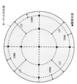
- the variation in the oxygen content is 9 locations in the target plane (1 location in the center, 4 locations at 1 ⁇ 2 radius on the two perpendicular diameters, and 4 locations 10 mm inside from the outer periphery.
- the oxygen content of each small piece (0.5 to 1 g) collected from (1) is measured using the LECO method.
- variation in oxygen content is computed from the following formula
- Oxygen content variation (%) (maximum value ⁇ minimum value) / average value ⁇ 100
- the Ti—Nb alloy sputtering target of the present invention preferably has a Vickers hardness of 400 Hv or less. More preferably, it is 300 Hv or less, More preferably, it is 200 Hv or less. The lower the Vickers hardness, the easier the plastic working, cutting, etc., and the better the finished shape of the target. A good surface property has an excellent effect that generation of particles during sputtering can be suppressed.
- the hardness of a metal or alloy usually decreases as the purity increases, it is conceivable to increase the refining ability and reduce impurities in order to obtain a low-hardness material.
- oxygen is a gas component and unlike other metal impurities, there is a limit to the reduction in the normal purification process.
- the present invention focuses on oxygen in the target (raw material), and realizes a high hardness target by reducing the oxygen concentration as much as possible even if the purity is 4N to 5N.
- the Vickers hardness of the Ti—Nb alloy sputtering target preferably has a variation within 10% within the target plane. If the in-plane variation of the Vickers hardness is more than 10%, the surface property changes depending on the location, and there is a possibility that uniform film formation becomes difficult.
- the surface roughness Ra of the sputtering target is preferably 1.0 ⁇ m or less.
- the hardness of the Ti—Nb alloy target can be reduced, so that cutting can be easily performed and the target has excellent surface properties with a surface roughness Ra of 1.0 ⁇ m or less. Can be produced. Thus, film formation characteristics can be improved.
- the surface roughness of the present invention is 9 locations in the plane of the target (1 location in the center, 4 locations at 1 ⁇ 2 radius on the two orthogonal diameters, and 10 mm inside from the outer periphery. About 4 positions), each surface roughness is measured using the measuring method of the surface property of JIS B 0601, and is averaged.
- the purity is preferably 4N (99.99%) or more and 5N (99.999%) or less.
- purity 4N is analyzed by glow discharge mass spectrometry (GDMS), and the total value of Na, Al, Si, K, Cr, Mn, Fe, Co, Ni, Cu, Zn, and Zr is less than 100 ppm. It means that. This is because if a large amount of impurities is contained, the film quality is deteriorated and desired film characteristics may not be obtained.
- the Ti—Nb alloy has a relationship in which the purity and the hardness are proportional, and the hardness can be lowered by increasing the purity. In the present invention, as shown in FIG.
- the purity is determined by slicing a portion 10 mm inside from the top surface or bottom surface of the ingot (target material) with a thickness of 2 mm to produce a disk-shaped sample, and a small piece (2 mm ⁇ 2 mm) from the center of the sample. X15 mm) is collected, analyzed by GDMS, and the impurity content is measured.
- the purity notation that contains Ta may be about 2N, but the presence of Ta does not hinder the characteristics of the barrier application.
- the Nb purity can be calculated from the metal impurities excluding Ta as described above.
- the density is higher than that produced by sintering powder.
- the relative density of the sintered body (target material) is about 97%, but in the present invention, a relative density of 99.9% or more can be achieved.
- Such a high-density target can contribute to particle suppression.
- the relative density in the present invention is represented by the ratio of the measured evaluation density of Ti—Nb evaluated by the Archimedes method to the theoretical density of Ti—Nb, as represented by the following formula.
- Relative density (%) (Archimedes density / theoretical density) ⁇ 100
- the theoretical density of Ti—Nb is expressed by the following equation when the ratio of Nb atoms in the target is N (%).
- Theoretical density (g / cm 3 ) (4787-45.04 ⁇ N) / (1061 ⁇ 0.227 ⁇ N)
- the Ti—Nb alloy sputtering target of the present invention can be produced by the following method.
- a Ti raw material having a purity of 4N or higher and an Nb raw material having a purity of 4N or higher are prepared so as to have a desired atomic ratio.
- the oxygen concentration increases when the surface area of the raw material is large, it is preferable to use a raw material with a small surface area.
- the Ti material is preferably tiled with a thickness of 1 mm to 5 mm and 10 mm square to 50 mm square, and the Nb material is 0.5 mm to 2 mm thick, 2 mm to 50 mm wide, and the length is appropriately selected.
- a plate-like or ribbon-like shape is preferable.
- the raw material having such a shape can be produced by adjusting the end material produced by cutting and grinding each metal material ingot to a certain size. In addition, after that, in order to remove the adhered dirt, washing, degreasing, and pickling as necessary are performed.
- the raw material is put into a vacuum skull melting furnace equipped with a water-cooled copper crucible of ⁇ 150 mm ⁇ 200 mmL and melted.
- the Nb raw material is added in multiple portions. This can be dissolved even when the Nb content is 0.1 to 3 at% simultaneously with the Ti material.
- the Nb content is in the range of 3 to 30 at%, the above-mentioned multiple times of follow-up is possible. This is because the uniformity of the dissolved material (including oxygen in the material) can be kept good by performing the addition of the Nb material by addition.
- the melt synthesis of a low Nb composition it is possible to promote the melt synthesis of a low Nb composition and maintain the fluidity of the melt at a melt temperature much lower than the Nb melting point of 2469 ° C., and Ti exposed to a high temperature near the melting point of Nb.
- the composition can be precisely controlled without scattering and volatilizing (melting point 1668 ° C.).
- the Ti—Nb alloy ingot is produced by cooling the Ti—Nb alloy melt prepared by melting all the raw materials prepared for the target composition in a water-cooled copper crucible. Thereafter, the ingot is hot forged at 700 to 1200 ° C., and then hot rolled at 700 to 1000 ° C. If necessary, secondary forging and secondary rolling can be performed.
- the present invention is not particularly limited by the above steps, and the number and temperature of forging and rolling can be appropriately selected for adjusting the shape and structure.
- the surface of the plastic-processed Ti—Nb alloy is machined such as cutting and polishing to finish the surface properties as desired.
- a Ti—Nb alloy sputtering target having the features of the present invention can be manufactured. And such a target can suppress generation
- Example 1 A 30 mm square, 2 mm thick Ti raw material (purity 4N or more) and a ribbon-like Nb raw material (purity 4N or more excluding Ta) having a width of 10 mm and a length of 1 mm are prepared, and these are 99.9 at% Ti.
- the Nb was weighed so as to be 0.1 at% and put into a melting furnace. Next, this was subjected to vacuum skull melting with an output that would dissolve the Ti material to form a Ti—Nb alloy, and then the molten alloy was cooled in a water-cooled copper crucible. Next, this Ti—Nb alloy ingot was hot forged at 700 ° C. and then hot rolled at 700 ° C. Thereafter, the plastic-processed Ti—Nb alloy was subjected to machining such as cutting and polishing to finish a desired surface property.
- the oxygen content was 380 wtppm (variation: 18%)
- the relative density was 100%
- the Vickers hardness was 150 Hv (variation: 10%)
- the surface roughness Ra was 0.4 ⁇ m.
- the sputtering conditions were as follows: the input power was 15 kW, the Ar gas flow rate was 8 sccm, 75 kWhr of pre-sputtering was performed, and then a film was formed on a 12-inch diameter silicon substrate for 15 seconds.
- the number of particles having a size of 0.1 ⁇ m or more adhered on the substrate was three. Further, as a result of performing a heat resistance test (heating at 700 ° C.) on the formed film, no peeling or the like was observed, and good adhesion and heat resistance were exhibited.
- Example 2 A 30 mm square, 2 mm thick Ti raw material (purity of 4 N or more) and a ribbon-shaped Nb raw material (purity excluding Ta of 4 N or more) of 10 mm width, 50 mm length and 1 mm thickness are prepared. It weighed so that it might become 2at%, and it injected into the melting furnace. Next, this was subjected to vacuum skull melting with an output that would dissolve the Ti material to form a Ti—Nb alloy, and then the molten alloy was cooled in a water-cooled copper crucible. Next, this Ti—Nb alloy ingot was hot forged at 700 ° C. and then hot rolled at 700 ° C. Thereafter, the plastic-processed Ti—Nb alloy was subjected to machining such as cutting and polishing to finish a desired surface property.
- the oxygen content was 350 wtppm (variation: 18%)
- the relative density was 100%
- the Vickers hardness was 180 Hv (variation: 10%)
- the surface roughness Ra was 0.4 ⁇ m.
- the sputtering conditions were as follows: the input power was 15 kW, the Ar gas flow rate was 8 sccm, 75 kWhr of pre-sputtering was performed, and then a film was formed on a 12-inch diameter silicon substrate for 15 seconds. The number of particles having a size of 0.1 ⁇ m or more adhered on the substrate was three. Further, as a result of performing a heat resistance test (heating at 700 ° C.) on the formed film, no peeling or the like was observed, and good adhesion and heat resistance were exhibited.
- Example 3 50 mm square, 5 mm thick Ti raw material (purity 4N or more) and 10 mm width, 50 mm length, 1 mm thick ribbon-like Nb raw material (purity excluding Ta 4N or more) are prepared. Weighed and prepared to 3at%. First, the Ti material was charged into the melting furnace, and the Nb material was set in a raw material charging mechanism for additional addition. Next, this was vacuum skull melted at an output that would dissolve the Ti material, and after confirming the dissolution of the Ti raw material, the Nb material was added in 10 portions. After forming a Ti—Nb alloy, the molten alloy was cooled in a water-cooled copper crucible.
- this Ti—Nb alloy ingot was hot forged at 1200 ° C. and then hot rolled at 1000 ° C. Thereafter, the plastic-processed Ti—Nb alloy was subjected to machining such as cutting and polishing to finish a desired surface property.
- the oxygen content was 330 wtppm (variation: 17%)
- the relative density was 100%
- the Vickers hardness was 190 Hv (variation: 8%)
- the surface roughness Ra was 0.4 ⁇ m.
- the target thus obtained was attached to a sputtering apparatus, and sputtering was performed.
- the sputtering conditions were the same as in Example 1.
- the number of particles having a size of 0.1 ⁇ m or more adhered on the substrate was five. Further, as a result of performing a heat resistance test (heating at 700 ° C.) on the formed film, no peeling or the like was observed, and good adhesion and heat resistance were exhibited.
- Example 4 50 mm square, 5 mm thick Ti raw material (purity 4N or higher) and 10 mm width, 50 mm length, 1 mm thick ribbon Nb raw material (purity 4N or higher excluding Ta) are prepared. It prepared by weighing so that it might become 10 at%. First, the Ti material was charged into the melting furnace, and the Nb material was set in a raw material charging mechanism for additional addition. Next, this was vacuum skull melted at an output that would dissolve the Ti material, and after confirming the dissolution of the Ti raw material, the Nb material was added in 10 portions. After forming a Ti—Nb alloy, the molten alloy was cooled in a water-cooled copper crucible.
- this Ti—Nb alloy ingot was hot forged at 1200 ° C. and then hot rolled at 1000 ° C. Thereafter, the plastic-processed Ti—Nb alloy was subjected to machining such as cutting and polishing to finish a desired surface property.
- the oxygen content was 260 wtppm (variation: 15%)
- the relative density was 100%
- the Vickers hardness was 220 Hv (variation: 8%)
- the surface roughness Ra was 0.5 ⁇ m.
- the target thus obtained was attached to a sputtering apparatus, and sputtering was performed.
- the sputtering conditions were the same as in Example 1.
- the number of particles having a size of 0.1 ⁇ m or more adhered on the substrate was nine. Further, as a result of performing a heat resistance test (heating at 700 ° C.) on the formed film, no peeling or the like was observed, and good adhesion and heat resistance were exhibited.
- Example 5 50 mm square, 5 mm thick Ti raw material (purity 4N or higher) and 10 mm width, 50 mm length, 1 mm thick ribbon Nb raw material (purity 4N or higher excluding Ta) are prepared. It prepared by weighing so that it might become 20at%. First, the Ti material was charged into the melting furnace, and the Nb material was set in a raw material charging mechanism for additional addition. Next, this was vacuum skull melted at an output that would dissolve the Ti material, and after confirming the dissolution of the Ti raw material, the Nb material was added in 10 portions. After forming a Ti—Nb alloy, the molten alloy was cooled in a water-cooled copper crucible.
- this Ti—Nb alloy ingot was hot forged at 1200 ° C. and then hot rolled at 1000 ° C. Thereafter, the plastic-processed Ti—Nb alloy was subjected to machining such as cutting and polishing to finish a desired surface property.
- the oxygen content was 200 wtppm (variation: 9%)
- the relative density was 100%
- the Vickers hardness was 360 Hv (variation: 8%)
- the surface roughness Ra was 0.7 ⁇ m.
- the target thus obtained was attached to a sputtering apparatus, and sputtering was performed.
- the sputtering conditions were the same as in Example 1.
- the number of particles having a size of 0.1 ⁇ m or more adhered on the substrate was seven. Further, as a result of performing a heat resistance test (heating at 700 ° C.) on the formed film, no peeling or the like was observed, and good adhesion and heat resistance were exhibited.
- Example 6 50 mm square, 5 mm thick Ti raw material (purity 4N or higher) and 10 mm width, 50 mm length, 1 mm thick ribbon Nb raw material (purity 4N or higher excluding Ta) are prepared. Weighed and prepared to be 30 at%. First, the Ti material was charged into the melting furnace, and the Nb material was set in a raw material charging mechanism for additional addition. Next, this was vacuum skull melted at an output that would dissolve the Ti material, and after confirming the dissolution of the Ti raw material, the Nb material was added in 10 portions. After forming a Ti—Nb alloy, the molten alloy was cooled in a water-cooled copper crucible.
- this Ti—Nb alloy ingot was hot forged at 1200 ° C. and then hot rolled at 1000 ° C. Thereafter, the plastic-processed Ti—Nb alloy was subjected to machining such as cutting and polishing to finish a desired surface property.
- the oxygen content was 160 wtppm (variation: 6%)
- the relative density was 100%
- the Vickers hardness was 390 Hv (variation: 7%)
- the surface roughness Ra was 0.8 ⁇ m.
- the target thus obtained was attached to a sputtering apparatus, and sputtering was performed.
- the sputtering conditions were the same as in Example 1.
- the number of particles having a size of 0.1 ⁇ m or more adhered on the substrate was six. Further, as a result of performing a heat resistance test (heating at 700 ° C.) on the formed film, no peeling or the like was observed, and good adhesion and heat resistance were exhibited.
- Comparative Example 1 Prepare Ti raw material (purity 4N or more) and Nb raw material (purity 4N or more excluding Ta) of 60mm square and 10mm thickness, and weigh them so that Ti is 99.9at% and Nb is 0.1at% And put into a melting furnace. First, the Ti material was charged into the melting furnace, and the Nb material was set in a raw material charging mechanism for additional addition. Next, this was vacuum skull dissolved at an output that would dissolve the Ti material, and after confirming the dissolution of the Ti raw material, the square Nb material was added all at once. Thereafter, the molten alloy was cooled in a water-cooled copper crucible. Next, this Ti—Nb alloy ingot was hot forged at 700 ° C.
- the composition varied in the range of 0.1 to 0.4 at%, the relative density could not be measured, the oxygen content was 360 wtppm (variation: 20%), the Vickers hardness was 220 Hv. (Variation 23%).
- a Ti raw material (purity of 4N or higher) and Nb raw material (purity of 4N or higher excluding Ta) of 60 mm square and 10 mm thickness were prepared and weighed and prepared such that Ti was 90 at% and Nb was 10 at%.
- the Ti material was charged into the melting furnace, and the Nb material was set in a raw material charging mechanism for additional addition.
- this Ti—Nb alloy ingot was hot forged at 1000 ° C. and then hot rolled at 1000 ° C. However, unmelted Nb material was observed, and slight cracking occurred during forging or rolling.
- the composition varied within a range of 5 to 40 at%, the relative density could not be measured, the oxygen content was 280 wtppm (variation: 30%), the Vickers hardness was 220 Hv (variation: 30 %).
- the composition varied in the range of 8 to 75 at%, the relative density could not be measured, the oxygen content was 220 wtppm (variation: 31%), the Vickers hardness was 330 Hv (variation: 30 %).
- Comparative Example 4 Ti powder and Nb powder were prepared so as to have an atomic composition ratio of 70:30, and these were mixed, and then sintered by holding at a temperature of 1300 ° C. for 2 hours by vacuum hot pressing. Thereafter, this Ti—Nb alloy sintered body was subjected to mechanical processing such as grinding and polishing, and finished to a desired surface property.
- oxygen content, relative density, Vickers hardness, and surface roughness were investigated. As a result, the oxygen content was 1500 wtppm (variation: 25%), relative density 98%, Vickers hardness 450 Hv (variation: 16%), and surface roughness Ra 1.2 ⁇ m.
- the target thus obtained was attached to a sputtering apparatus, and sputtering was performed.
- the sputtering conditions were the same as in Example 1.
- the number of particles having a size of 0.1 ⁇ m or more adhered on the substrate was 1200. Further, as a result of performing a heat resistance test (heating at 700 ° C.) on the formed film, peeling was observed.
- Comparative Example 5 A Ti raw material and an Nb raw material were prepared so as to have an atomic composition ratio of 90:10, and these were pulverized by an atomizing process, and then held and sintered at a temperature of 1300 ° C. for 2 hours by vacuum hot pressing. Thereafter, this Ti—Nb alloy sintered body was subjected to mechanical processing such as grinding and polishing, and finished to a desired surface property. About the sputtering target obtained by the above process, oxygen content, relative density, Vickers hardness, and surface roughness were investigated.
- the oxygen content was 800 wtppm (variation: 15%), the relative density was 98%, the Vickers hardness was 420 Hv (variation: 10%), and the surface roughness Ra was 1.0 ⁇ m.
- the target thus obtained was attached to a sputtering apparatus, and sputtering was performed.
- the sputtering conditions were the same as in Example 1.
- the number of particles having a size of 0.1 ⁇ m or more adhered on the substrate was 350. Further, as a result of performing a heat resistance test (heating at 700 ° C.) on the formed film, peeling was observed.
- the present invention is a Ti—Nb alloy tantalum sputtering target, which has a low oxygen content, low hardness, and is easy to process and has good surface properties, and therefore can suppress generation of particles during sputtering. It has an excellent effect.
- the present invention is useful as Ti—Nb alloy sputtering suitable for forming a thin film for element wiring of a semiconductor integrated circuit.
Landscapes
- Chemical & Material Sciences (AREA)
- Engineering & Computer Science (AREA)
- Mechanical Engineering (AREA)
- Metallurgy (AREA)
- Organic Chemistry (AREA)
- Materials Engineering (AREA)
- Physics & Mathematics (AREA)
- Crystallography & Structural Chemistry (AREA)
- Thermal Sciences (AREA)
- Chemical Kinetics & Catalysis (AREA)
- Plasma & Fusion (AREA)
- Analytical Chemistry (AREA)
- Physical Vapour Deposition (AREA)
- Electrodes Of Semiconductors (AREA)
Abstract
Priority Applications (5)
| Application Number | Priority Date | Filing Date | Title |
|---|---|---|---|
| JP2017555409A JP6440866B2 (ja) | 2016-03-25 | 2017-03-23 | Ti−Nb合金スパッタリングターゲット及びその製造方法 |
| US16/088,118 US11837449B2 (en) | 2016-03-25 | 2017-03-23 | Ti-Nb alloy sputtering target and production method thereof |
| KR1020187026284A KR102236414B1 (ko) | 2016-03-25 | 2017-03-23 | Ti-Nb 합금 스퍼터링 타깃 및 그 제조 방법 |
| EP17770342.8A EP3418422B1 (fr) | 2016-03-25 | 2017-03-23 | Cible de pulvérisation en alliage ti-nb et procédé pour la fabriquer |
| SG11201808205QA SG11201808205QA (en) | 2016-03-25 | 2017-03-23 | Ti-Nb ALLOY SPUTTERING TARGET AND PRODUCTION METHOD THEREOF |
Applications Claiming Priority (2)
| Application Number | Priority Date | Filing Date | Title |
|---|---|---|---|
| JP2016062545 | 2016-03-25 | ||
| JP2016-062545 | 2016-03-25 |
Publications (1)
| Publication Number | Publication Date |
|---|---|
| WO2017164302A1 true WO2017164302A1 (fr) | 2017-09-28 |
Family
ID=59900250
Family Applications (1)
| Application Number | Title | Priority Date | Filing Date |
|---|---|---|---|
| PCT/JP2017/011696 Ceased WO2017164302A1 (fr) | 2016-03-25 | 2017-03-23 | CIBLE DE PULVÉRISATION EN ALLIAGE Ti-Nb ET PROCÉDÉ POUR LA FABRIQUER |
Country Status (7)
| Country | Link |
|---|---|
| US (1) | US11837449B2 (fr) |
| EP (1) | EP3418422B1 (fr) |
| JP (1) | JP6440866B2 (fr) |
| KR (1) | KR102236414B1 (fr) |
| SG (1) | SG11201808205QA (fr) |
| TW (1) | TWI721139B (fr) |
| WO (1) | WO2017164302A1 (fr) |
Cited By (1)
| Publication number | Priority date | Publication date | Assignee | Title |
|---|---|---|---|---|
| WO2024236783A1 (fr) * | 2023-05-17 | 2024-11-21 | 住友電気工業株式会社 | Matériau de titane, élément médical, élément de constitution d'implant dentaire et capsule de logement de capteur de diamant |
Families Citing this family (2)
| Publication number | Priority date | Publication date | Assignee | Title |
|---|---|---|---|---|
| CN111057905B (zh) * | 2020-01-13 | 2022-03-04 | 西安理工大学 | 一种粉末冶金制备铌钛合金的方法 |
| CN113290178B (zh) * | 2021-05-21 | 2022-04-19 | 东莞市诺德金属科技有限公司 | 一种高Nb含量Ti-Nb合金铸锭开坯锻造方法 |
Citations (3)
| Publication number | Priority date | Publication date | Assignee | Title |
|---|---|---|---|---|
| WO2010110412A1 (fr) * | 2009-03-27 | 2010-09-30 | 日鉱金属株式会社 | Cible de pulvérisation de corps fritté d'oxyde de ti - nb, mince film d'oxyde de ti - nb et procédé de fabrication du mince film |
| JP2012507626A (ja) * | 2008-11-03 | 2012-03-29 | トーソー エスエムディー,インク. | スパッターターゲットを製造する方法と当該方法によって製造されるスパッターターゲット |
| JP2013194276A (ja) * | 2012-03-19 | 2013-09-30 | Citizen Holdings Co Ltd | 金色硬質装飾部材 |
Family Cites Families (17)
| Publication number | Priority date | Publication date | Assignee | Title |
|---|---|---|---|---|
| JPS5197393A (en) | 1975-02-21 | 1976-08-26 | x senshutsuryokuno seigyohoho | |
| JPH01290766A (ja) | 1988-05-18 | 1989-11-22 | Nippon Mining Co Ltd | Ti含有高純度Taターゲット及びその製造方法 |
| US5224534A (en) * | 1990-09-21 | 1993-07-06 | Nippon Mining And Metals Company, Limited | Method of producing refractory metal or alloy materials |
| US5102450A (en) * | 1991-08-01 | 1992-04-07 | General Electric Company | Method for melting titanium aluminide alloys in ceramic crucible |
| US6309556B1 (en) * | 1998-09-03 | 2001-10-30 | Praxair S.T. Technology, Inc. | Method of manufacturing enhanced finish sputtering targets |
| US6348113B1 (en) * | 1998-11-25 | 2002-02-19 | Cabot Corporation | High purity tantalum, products containing the same, and methods of making the same |
| US6331484B1 (en) | 1999-03-29 | 2001-12-18 | Lucent Technologies, Inc. | Titanium-tantalum barrier layer film and method for forming the same |
| JP3445557B2 (ja) | 1999-05-24 | 2003-09-08 | ルーセント テクノロジーズ インコーポレーテッド | チタン−タンタル障壁層薄膜及びその形成方法 |
| JP2001131737A (ja) * | 1999-11-09 | 2001-05-15 | Nikko Materials Co Ltd | スパッタリングターゲット及びその研削方法 |
| TWI256420B (en) * | 2000-04-20 | 2006-06-11 | Toshiba Corp | Sputter target, barrier film and electronic component |
| US20030227068A1 (en) | 2001-05-31 | 2003-12-11 | Jianxing Li | Sputtering target |
| AU2001275184A1 (en) | 2000-08-15 | 2002-02-25 | Honeywell International, Inc. | Sputtering target |
| JP3898044B2 (ja) * | 2001-12-03 | 2007-03-28 | 株式会社東芝 | スパッタリングターゲット |
| JP4923933B2 (ja) | 2006-10-10 | 2012-04-25 | 東京エレクトロン株式会社 | バリヤ層の形成方法及びプラズマ成膜装置 |
| JP2010123586A (ja) | 2008-11-17 | 2010-06-03 | Nec Electronics Corp | 半導体装置、半導体装置の製造方法 |
| JP5550328B2 (ja) * | 2009-12-22 | 2014-07-16 | 株式会社東芝 | Moスパッタリングターゲットおよびその製造方法 |
| JP5701879B2 (ja) | 2010-07-16 | 2015-04-15 | Jx日鉱日石金属株式会社 | タンタル基焼結体スパッタリングターゲットの製造方法 |
-
2017
- 2017-03-23 WO PCT/JP2017/011696 patent/WO2017164302A1/fr not_active Ceased
- 2017-03-23 EP EP17770342.8A patent/EP3418422B1/fr active Active
- 2017-03-23 KR KR1020187026284A patent/KR102236414B1/ko active Active
- 2017-03-23 SG SG11201808205QA patent/SG11201808205QA/en unknown
- 2017-03-23 US US16/088,118 patent/US11837449B2/en active Active
- 2017-03-23 JP JP2017555409A patent/JP6440866B2/ja active Active
- 2017-03-24 TW TW106109928A patent/TWI721139B/zh active
Patent Citations (3)
| Publication number | Priority date | Publication date | Assignee | Title |
|---|---|---|---|---|
| JP2012507626A (ja) * | 2008-11-03 | 2012-03-29 | トーソー エスエムディー,インク. | スパッターターゲットを製造する方法と当該方法によって製造されるスパッターターゲット |
| WO2010110412A1 (fr) * | 2009-03-27 | 2010-09-30 | 日鉱金属株式会社 | Cible de pulvérisation de corps fritté d'oxyde de ti - nb, mince film d'oxyde de ti - nb et procédé de fabrication du mince film |
| JP2013194276A (ja) * | 2012-03-19 | 2013-09-30 | Citizen Holdings Co Ltd | 金色硬質装飾部材 |
Cited By (1)
| Publication number | Priority date | Publication date | Assignee | Title |
|---|---|---|---|---|
| WO2024236783A1 (fr) * | 2023-05-17 | 2024-11-21 | 住友電気工業株式会社 | Matériau de titane, élément médical, élément de constitution d'implant dentaire et capsule de logement de capteur de diamant |
Also Published As
| Publication number | Publication date |
|---|---|
| TW201805461A (zh) | 2018-02-16 |
| US20190115196A1 (en) | 2019-04-18 |
| EP3418422A4 (fr) | 2019-10-30 |
| TWI721139B (zh) | 2021-03-11 |
| JPWO2017164302A1 (ja) | 2018-03-29 |
| KR20180110111A (ko) | 2018-10-08 |
| EP3418422B1 (fr) | 2022-06-22 |
| SG11201808205QA (en) | 2018-10-30 |
| JP6440866B2 (ja) | 2018-12-19 |
| US11837449B2 (en) | 2023-12-05 |
| EP3418422A1 (fr) | 2018-12-26 |
| KR102236414B1 (ko) | 2021-04-05 |
Similar Documents
| Publication | Publication Date | Title |
|---|---|---|
| JP6356357B2 (ja) | Ti−Ta合金スパッタリングターゲット及びその製造方法 | |
| TWI419987B (zh) | Tantalum sputtering target | |
| TWI413703B (zh) | Tantalum sputtering target | |
| TWI419986B (zh) | Tantalum sputtering target | |
| TWI500778B (zh) | Tantalum sputtering target | |
| TWI503420B (zh) | Tantalum sputtering target | |
| KR20170141280A (ko) | 탄탈 스퍼터링 타깃 | |
| JP6440866B2 (ja) | Ti−Nb合金スパッタリングターゲット及びその製造方法 |
Legal Events
| Date | Code | Title | Description |
|---|---|---|---|
| ENP | Entry into the national phase |
Ref document number: 2017555409 Country of ref document: JP Kind code of ref document: A |
|
| ENP | Entry into the national phase |
Ref document number: 20187026284 Country of ref document: KR Kind code of ref document: A |
|
| WWE | Wipo information: entry into national phase |
Ref document number: 1020187026284 Country of ref document: KR |
|
| WWE | Wipo information: entry into national phase |
Ref document number: 2017770342 Country of ref document: EP |
|
| WWE | Wipo information: entry into national phase |
Ref document number: 11201808205Q Country of ref document: SG |
|
| NENP | Non-entry into the national phase |
Ref country code: DE |
|
| ENP | Entry into the national phase |
Ref document number: 2017770342 Country of ref document: EP Effective date: 20180919 |
|
| 121 | Ep: the epo has been informed by wipo that ep was designated in this application |
Ref document number: 17770342 Country of ref document: EP Kind code of ref document: A1 |