WO2017164309A1 - 光学体及び発光装置 - Google Patents
光学体及び発光装置 Download PDFInfo
- Publication number
- WO2017164309A1 WO2017164309A1 PCT/JP2017/011729 JP2017011729W WO2017164309A1 WO 2017164309 A1 WO2017164309 A1 WO 2017164309A1 JP 2017011729 W JP2017011729 W JP 2017011729W WO 2017164309 A1 WO2017164309 A1 WO 2017164309A1
- Authority
- WO
- WIPO (PCT)
- Prior art keywords
- uneven structure
- micro
- macro
- optical body
- light
- Prior art date
- Legal status (The legal status is an assumption and is not a legal conclusion. Google has not performed a legal analysis and makes no representation as to the accuracy of the status listed.)
- Ceased
Links
Images


Classifications
-
- G—PHYSICS
- G02—OPTICS
- G02B—OPTICAL ELEMENTS, SYSTEMS OR APPARATUS
- G02B5/00—Optical elements other than lenses
- G02B5/04—Prisms
- G02B5/045—Prism arrays
-
- G—PHYSICS
- G02—OPTICS
- G02B—OPTICAL ELEMENTS, SYSTEMS OR APPARATUS
- G02B1/00—Optical elements characterised by the material of which they are made; Optical coatings for optical elements
- G02B1/10—Optical coatings produced by application to, or surface treatment of, optical elements
- G02B1/11—Anti-reflection coatings
- G02B1/118—Anti-reflection coatings having sub-optical wavelength surface structures designed to provide an enhanced transmittance, e.g. moth-eye structures
-
- G—PHYSICS
- G02—OPTICS
- G02B—OPTICAL ELEMENTS, SYSTEMS OR APPARATUS
- G02B6/00—Light guides; Structural details of arrangements comprising light guides and other optical elements, e.g. couplings
- G02B6/0001—Light guides; Structural details of arrangements comprising light guides and other optical elements, e.g. couplings specially adapted for lighting devices or systems
- G02B6/0011—Light guides; Structural details of arrangements comprising light guides and other optical elements, e.g. couplings specially adapted for lighting devices or systems the light guides being planar or of plate-like form
- G02B6/0033—Means for improving the coupling-out of light from the light guide
- G02B6/0035—Means for improving the coupling-out of light from the light guide provided on the surface of the light guide or in the bulk of it
- G02B6/0036—2-D arrangement of prisms, protrusions, indentations or roughened surfaces
-
- G—PHYSICS
- G02—OPTICS
- G02B—OPTICAL ELEMENTS, SYSTEMS OR APPARATUS
- G02B6/00—Light guides; Structural details of arrangements comprising light guides and other optical elements, e.g. couplings
- G02B6/0001—Light guides; Structural details of arrangements comprising light guides and other optical elements, e.g. couplings specially adapted for lighting devices or systems
- G02B6/0011—Light guides; Structural details of arrangements comprising light guides and other optical elements, e.g. couplings specially adapted for lighting devices or systems the light guides being planar or of plate-like form
- G02B6/0033—Means for improving the coupling-out of light from the light guide
- G02B6/0035—Means for improving the coupling-out of light from the light guide provided on the surface of the light guide or in the bulk of it
- G02B6/0045—Means for improving the coupling-out of light from the light guide provided on the surface of the light guide or in the bulk of it by shaping at least a portion of the light guide
-
- G—PHYSICS
- G02—OPTICS
- G02B—OPTICAL ELEMENTS, SYSTEMS OR APPARATUS
- G02B6/00—Light guides; Structural details of arrangements comprising light guides and other optical elements, e.g. couplings
- G02B6/0001—Light guides; Structural details of arrangements comprising light guides and other optical elements, e.g. couplings specially adapted for lighting devices or systems
- G02B6/0011—Light guides; Structural details of arrangements comprising light guides and other optical elements, e.g. couplings specially adapted for lighting devices or systems the light guides being planar or of plate-like form
- G02B6/0065—Manufacturing aspects; Material aspects
Definitions
- the present invention relates to an optical body and a light emitting device.
- an optical body that combines a light guiding phenomenon and a macro uneven structure is known.
- Such an optical body is also referred to as a light guide plate.
- the macro uneven structure is formed on one surface of the light guide plate.
- Light incident on the inside of the light guide plate, that is, internally propagated light propagates inside the light guide plate while being reflected by the surface of the light guide plate (that is, the interface between the inside and outside of the light guide plate). Thereafter, the internally propagating light is reflected by the surface of the macro uneven structure and emitted from the other surface of the light guide plate.
- the light guide plate emits light incident from the side surface of the light guide plate from the surface of the light guide plate.
- the light guide plate is used as a light emitter for various display devices or a light emitter for illumination, for example.
- Examples of the display device in which the light guide plate is used include various types of LCDs (for example, local dimming drive type LCDs), passive type display devices, light decoration panels for amusements, and illumination panels for advertising such as digital signage. It is done. In these display devices, it is possible to make an expression as if light is lifted from a portion where a pattern of the macro uneven structure is formed by turning on and off the light source.
- the slope of at least one surface of the macro uneven structure needs to be a slope of 30 ° or more and less than 90 °.
- Light that enters from the side surface of the light guide plate and travels through the light guide plate is totally reflected by the inclined surface and is emitted from the surface of the light guide plate.
- external light in addition to sunlight, light from other light emitters (for example, illumination, other display devices, etc.), other display bodies (for example, liquid crystal panels, etc.) provided in the display device, etc.
- the light from other light emitters for example, illumination, other display devices, etc.
- other display bodies for example, liquid crystal panels, etc.
- JP 2006-012854 A Japanese Patent Laid-Open No. 2003-249110 JP 2008-299079 A
- Patent Documents 1 to 3 disclose techniques related to the above-described light guide plate.
- a micro uneven structure having an average period of unevenness of a visible light wavelength or less is provided on at least one surface of both surfaces of the light guide plate.
- the micro concavo-convex structure is randomly arranged. Further, the distance between the convex portions or the distance between the concave portions of the micro uneven structure satisfies a predetermined condition.
- the present invention has been made in view of the above problems, and the object of the present invention is to be used as a light guide plate and to have an excellent antireflection function for extraneous light. It is an object of the present invention to provide a new and improved optical body and light emitting device.
- a base material and internal propagation light formed on one surface of the base material and incident on the inside of the base material from the side surface of the base material are used.
- the surface of the macro concavo-convex structure has an inclined surface inclined at 30 ° or more and less than 90 ° with respect to one surface, and the arrangement of the micro concavo-convex structure is arranged in a staggered arrangement with respect to the traveling direction of the internal propagation light.
- An optical body is provided.
- the angle formed between the arrangement direction of the micro concavo-convex structure and the direction perpendicular to the propagation direction of the internal propagation light may be 30 to 60 °.
- one surface may be divided into a light emitting region in which a macro uneven structure is formed and a non-light emitting region other than the light emitting region, and the micro uneven structure may be formed in both the light emitting region and the non-light emitting region.
- micro uneven structure may extend in a direction perpendicular to the surface of the macro uneven structure.
- the macro uneven structure is an aggregate of a plurality of macro convex portions and macro concave portions, and at least one of the plurality of macro convex portions and macro concave portions has a prism shape. You may form according to each surface of a macro convex part and a macro recessed part.
- the luminous reflectance may be 1.0% or less.
- reflection chromaticities a * and b * may be 1.0 or less.
- the average height of the micro uneven structure may be 200 nm or more.
- the base material may have a multilayer structure.
- a light emitting device comprising: the optical body described above; and a light source that is provided on a side surface of the optical body and that makes light enter the inside of the optical body from the side surface of the optical body.
- the macro uneven structure formed on the surface of the optical body emits internally propagating light incident on the inside of the base material from the side surface of the base material from the other surface of the base material. be able to. Therefore, the optical body can be used as a light guide plate. Furthermore, the micro concavo-convex structure is periodically formed following both surfaces of the base material and the surface of the macro concavo-convex structure, and the average period of the concavo-convex is equal to or less than the visible light wavelength. Therefore, the optical body has an excellent antireflection function for extraneous light.
- FIG. 1 is a side sectional view showing a schematic configuration of an optical body according to Example 1.
- FIG. 6 is a side sectional view showing a schematic configuration of an optical body according to Example 2.
- FIG. FIG. 1 is a side sectional view showing a schematic configuration of an optical body according to Example 1.
- 6 is a side sectional view showing a schematic configuration of an optical body according to Example 3. It is a cross-sectional SEM photograph which shows a micro uneven structure. It is a cross-sectional SEM photograph which shows the micro uneven structure formed in accordance with the surface of a macro uneven structure. It is a plane SEM photograph which shows a micro uneven structure. 6 is a side sectional view showing a schematic configuration of an optical body according to Comparative Example 1.
- FIG. 10 is a side sectional view showing a schematic configuration of an optical body according to Comparative Example 2.
- FIG. 6 is a planar SEM photograph showing a micro uneven structure according to Comparative Example 4.
- 10 is a planar SEM photograph showing a micro uneven structure according to Comparative Example 5.
- 4 is a graph showing a comparison of specular reflection spectra of optical bodies according to Examples 1 to 3 and Comparative Examples 1 to 3.
- FIG. 6 is a graph showing a comparison of diffuse reflection spectra of optical bodies according to Examples 1 to 3 and Comparative Examples 1 to 3. It is a graph which shows the correspondence of the incident angle of measurement light, and reflection Y value (luminous reflectance) for every height of a micro uneven structure.
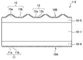
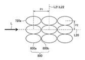
- the optical body 1 includes a substrate 10, a first micro uneven structure 11, a second micro uneven structure 12, and a macro uneven structure 13.
- the optical body 1 can function as a so-called light guide plate. That is, the optical body 1 emits internally propagating light incident on the optical body 1 from the side surface of the optical body 1 from the surface of the optical body 1 (specifically, a first surface 10A described later) to the outside.
- the base material 10 propagates the light incident on the inside of the base material 10, that is, internally propagated light, in the surface direction of the base material 10 (that is, the direction perpendicular to the thickness direction, the horizontal direction in FIG. 1). Further, although details will be described later, the optical body 1 is a macro uneven surface master having a reversed shape of the macro uneven structure 13 on the base material 10 on which the first micro uneven structure 11 and the second micro uneven structure 12 are formed. It is made by pressing under heating. Therefore, the base material 10 is required to be softened under heating. Therefore, it is preferable that the base material 10 is comprised with the thermoplastic resin excellent in light conductivity.
- the thickness of the substrate 10 is not particularly limited, and may be adjusted as appropriate depending on the use of the optical body 1 and the like.
- the substrate 10 may have a multilayer structure. For example, even if the optical body 1 is manufactured by bonding the base material on which the first micro uneven structure 11 is formed and the base material on which the second micro uneven structure 12 and the macro uneven structure 13 are formed, Good.
- the base material in which the 1st micro concavo-convex structure 11 was formed, the 2nd micro concavo-convex structure 12, and the macro concavo-convex structure 13 were formed in the both surfaces of the base material comprised with resin other than a thermoplastic resin. You may bond together a base material.
- the base material on which the second micro uneven structure 12 and the macro uneven structure 13 are formed is made of a thermoplastic resin.
- the first micro concavo-convex structure 11 is periodically formed in accordance with the surface 10A (hereinafter also referred to as the first surface) 10A of the substrate 10. That is, the first micro uneven structure 11 extends in a direction perpendicular to the first surface 10A.
- the average period of the concavo-convex is not more than the visible light wavelength (for example, 830 nm or less).
- the average period of the irregularities is preferably 100 nm or more and 350 nm or less, more preferably 120 nm or more and 280 nm or less, and further preferably 130 to 270 nm. Therefore, the first micro uneven structure 11 has a so-called moth-eye structure.
- the average period when the average period is less than 100 nm, it may be difficult to form the first micro uneven structure 11, which is not preferable. Further, when the average period exceeds 350 nm, the intensity of diffracted light may increase. That is, the internally propagating light may be diffracted by the first surface 10A and leaked to the outside.
- the first micro concavo-convex structure 11 has a large number of first micro convex portions 11a and first micro concave portions 11b.
- the first micro convex portion 11 a has a shape protruding outward in the thickness direction of the optical body 1
- the first micro concave portion 11 b has a shape recessed in the thickness direction of the optical body 1.
- the first micro convex portion 11a and the first micro concave portion 11b are periodically formed on the first surface 10A.
- the first micro concavo-convex structure 11 is a structure in which tracks (rows) composed of a plurality of first micro convex portions 11a and first micro concave portions 11b are arranged in parallel to each other.
- the tracks extend in the left-right direction and are aligned in the up-down direction.
- the first micro convex portion 11a (or the first micro concave portion 11b) disposed between adjacent tracks is half the length of the first micro convex portion 11a (or the first micro concave portion 11b). Only shifted in the track length direction.
- the average period of the irregularities is given as an arithmetic average value of the dot pitch P1 and the track pitch P2.
- the dot pitch P1 is a distance between the first micro convex portions 11a (or the first micro concave portions 11b) arranged in the track length direction.
- the track pitch P2 is a distance between adjacent tracks. In this embodiment, both the dot pitch P1 and the track pitch P2 are less than or equal to the visible light wavelength.
- the dot pitch P1 and the track pitch P2 may be the same or different.
- the dot pitch P1 is a distance between the first micro convex portions 11a (or the first micro concave portions 11b) arranged in the track length direction.
- the first micro concavo-convex structure 11 can be observed by, for example, a scanning electron microscope (SEM) or a cross-sectional transmission electron microscope (cross-section TEM).
- the dot pitch P1 is measured by the following method, for example. That is, a combination of the first micro-projections 11a adjacent in the track length direction is picked up.
- the distance between the vertices of the first micro-projections 11a may be the dot pitch P1.
- the track pitch P2 is a distance between adjacent tracks.
- the track pitch P2 is measured by the following method, for example. That is, a combination of adjacent tracks is picked up.
- the distance between the tracks may be the track pitch P2.
- the arrangement direction of the first micro concavo-convex structure 11 is divided into two arrangement directions, that is, a dot arrangement direction L20 and a cross arrangement direction L22.
- the dot arrangement direction L20 coincides with the track extending direction.
- the intersecting arrangement direction L22 is defined as a direction connecting the vertices of the first micro convex portions 11a (or the first micro concave portions 11b) adjacent to each other in the track arranging direction (here, the vertical direction).
- the angle between at least one of the dot arrangement direction L20 and the cross arrangement direction L21 and the straight line L21 perpendicular to the propagation direction L of the internal propagation light is 30 to 60 °. preferable.
- the angle ⁇ formed by the intersecting arrangement direction L22 and the straight line L21 is 30 to 60 °.
- the propagation direction L of the internal propagation light is defined as the propagation direction of the internal propagation light incident perpendicularly to the side surface of the substrate 10. Therefore, the propagation direction L is parallel to the surface direction of the substrate 10. Further, the plane whose normal is the propagation direction L and the surface direction of the substrate 10 intersect perpendicularly.
- the first micro concavo-convex structures 11 are arranged in a staggered pattern with respect to the traveling direction of the internally propagating light. That is, the traveling direction of the internal propagation light and the dot arrangement direction of the first micro concavo-convex structure 11 substantially coincide.
- the arrangement of the first micro uneven structure 11 is not limited to this example. That is, any arrangement is possible as long as the above-described requirements are satisfied.
- the first micro uneven structure 11 may be arranged in a rectangular lattice shape.
- the average height of the first micro uneven structure 11 is not particularly limited. That is, the average height of the first micro uneven structure 11 may be the same as or different from the average height of the second micro uneven structure 12.
- the average height of the first micro uneven structure 11 is preferably 100 nm to 300 nm, more preferably 130 nm. It is not less than 300 nm, more preferably not less than 150 nm and not more than 230 nm.
- the average height of the 1st micro uneven structure 11 is an arithmetic average value of the height of the 1st micro convex part 11a.
- the height of the 1st micro convex part 11a can be measured with the observation method mentioned above. That is, several heights of the first micro-projections 11 a are measured, and the arithmetic average value thereof may be set as the average height of the first micro-concave structure 11.
- the first micro convex portion 11a extends in a direction perpendicular to the first surface 10A.
- the second micro concavo-convex structure 12 is periodically formed along the surface (hereinafter also referred to as “second surface”) 10 ⁇ / b> B of the base material 10. That is, the second micro concavo-convex structure 12 extends in a direction perpendicular to the second surface 10B.
- the second micro uneven structure 12 has the same characteristics as the first micro uneven structure 11. That is, in the second micro concavo-convex structure 12, the average period of the concavo-convex is not more than the visible light wavelength (for example, 830 nm or less).
- the average period of the irregularities is preferably 100 nm or more and 350 nm or less, more preferably 120 nm or more and 280 nm or less, and further preferably 130 to 270 nm. Therefore, the second micro uneven structure 12 has a so-called moth-eye structure.
- the average period is less than 100 nm, it may be difficult to form the second micro uneven structure 12, which is not preferable.
- the average period exceeds 350 nm, the intensity of diffracted light may increase. That is, the internally propagating light may be diffracted by the second surface 10B and leaked to the outside.
- the second micro uneven structure 12 has a large number of second micro convex parts 12a and second micro concave parts 12b.
- the second micro convex portion 12 a has a shape protruding outward in the thickness direction of the optical body 1
- the second micro concave portion 12 b has a shape recessed in the thickness direction of the optical body 1.
- the second micro convex portion 12a and the second micro concave portion 12b are periodically formed on the second surface 10B.
- the arrangement of the second micro uneven structure 12 is the same as the arrangement of the first micro uneven structure 11.
- the arrangement direction of the second micro concavo-convex structure 12 is divided into two arrangement directions, that is, a dot arrangement direction L20 and a cross arrangement direction L22.
- an angle between at least one of the dot arrangement direction L20 and the cross arrangement direction L22 and a straight line L21 perpendicular to the propagation direction L of the internal propagation light is 30 to 60 °.
- the second micro uneven structure 12 is provided in both the region where the macro uneven structure 13 is formed, that is, the light emitting region 10D and the non-light emitting region 10C where the macro uneven structure 13 is not formed.
- the non-light emitting region 10C is a region other than the light emitting region 10D in the second surface 10B.
- the micro uneven structure 12 is formed following the surface of the non-light emitting region 10C. That is, the micro uneven structure 12 extends in a direction perpendicular to the surface of the non-light emitting region 10C.
- the macro uneven structure 13 is formed in the light emitting region 10D. Therefore, when light enters the optical body 1 from the light source 20, the internally propagated light is reflected by the macro uneven structure 13 in the light emitting region 10 ⁇ / b> D and emitted to the outside of the optical body 1. As a result, light is emitted from a region of the first surface 10A facing the light emitting region 10D. Accordingly, the light emitting region 10D is a region that emits internally propagating light. On the other hand, the macro uneven structure 13 is not formed in the non-light emitting region 10C. Therefore, light is not emitted from the region of the first surface 10A facing the non-light emitting region 10C.
- the second micro uneven structure 12 is formed following the surface of the macro uneven structure 13. That is, the second micro convex portion 12 a extends in a direction perpendicular to the surface of the macro uneven structure 13.
- the average height of the second micro uneven structure 12 is preferably 200 nm or more. Thereby, the antireflection function on the macro uneven structure 13 can be further enhanced.
- the upper limit value of the average height of the second micro concavo-convex structure 12 is not particularly limited, but is preferably 300 nm or less.
- the micro uneven structure 12 is provided in both the light emitting region 12D and the non-light emitting region 12C.
- the optical body 1 when used as a light guide plate, it is necessary to prevent the non-light emitting area from being recognized as much as possible by the viewer. Furthermore, it is necessary to prevent the viewer from recognizing the presence of the optical body 1 as much as possible when the light source is turned off. For this reason, in both the light emitting region 13D and the non-light emitting region 13C, an excellent antireflection function for extraneous light such as high transmission, low reflection, and low scattering is required. For this reason, in this embodiment, the micro uneven structure 12 is provided in both the light emitting region 12D and the non-light emitting region 12C.
- the first micro concavo-convex structure 11 and the second micro concavo-convex structure 12 may be integrally formed with the base material 10 or may be separate structures from the base material 10. Moreover, the uneven
- the macro uneven structure 13 is formed on a part of the second surface 10B.
- the macro uneven structure 13 is an aggregate of a plurality of macro convex portions 13a and macro concave portions 13b.
- the macro recess 13b has a shape that is recessed in the thickness direction of the optical body 1 with respect to the non-light emitting region 10C. Furthermore, the macro recessed part 13b may have what is called a prism shape. That is, the macro concave portion 13b is a long concave portion that extends in any plane direction of the second surface 10B (a direction perpendicular to the thickness direction of the optical body 1). In the example of FIG. 1, the macro recess 13b extends in a direction perpendicular to the paper surface.
- the shape of the macro recessed part 13b is not limited to this.
- the macro convex part 13a is arrange
- the vertices of the macro convex portions 13a are arranged in substantially the same plane as the non-light emitting region 10C. Therefore, although the details will be described later, the macro uneven structure 13 is formed by pressing a macro uneven surface master (see FIGS. 5 and 6) having an inverted shape of the macro recessed portion 13 b against the second micro uneven structure 12.
- the macro concave portion 13 b emits the internal propagation light toward the outside of the optical body 1. That is, the internally propagating light is reflected on the surface of the macro recess 13b.
- the specific shape of the macro uneven structure 13 is not particularly limited as long as it is the same shape as the macro uneven structure employed in the light guide plate.
- the macro recess 13b preferably has an inclined surface inclined with respect to the second surface 10B, and the angle ⁇ 1 formed by these is preferably 30 ° or more and less than 90 °.
- the macro concave portion 13b can emit the internal propagation light to the outside of the optical body 1 more reliably.
- the macro uneven structure 13 is formed on a part of the second surface 10B. For this reason, as described above, the second surface 10B is divided into a non-light emitting region 10C and a light emitting region 10D. Of course, the macro uneven structure 13 may be formed on the entire surface of the second surface 10B. In this case, the entire second surface 10B becomes the light emitting region 10D. In addition, the entire surface of the first surface 10A emits light.
- the shape of the macro uneven structure 13 is not limited to the example shown in FIG.
- the macro uneven structure 13 may have the inverted shape of FIG.
- the macro convex portion 13a has a shape protruding in the thickness direction of the optical body 1 with respect to the non-light emitting region 10C.
- the macro convex part 13a has what is called a prism shape.
- the internally propagating light is reflected by the surface of the macro convex portion 13a and is emitted to the outside of the optical body 1A.
- the angle formed between the inclined surface of the macro convex portion 13a and the second surface 10B is 30 ° or more and less than 90 °.
- the macro concave portion 13b can emit the internal propagation light to the outside of the optical body 1 more reliably.
- the micro concavo-convex structure 12 is formed following the inclined surface of the macro convex portion 13a.
- a micro uneven structure may be selectively formed only at least on the flat portions (here, the first surface 10A and the non-light emitting region 10C).
- the macro uneven structure 13 may not have a micro uneven structure.
- the luminous reflectance of the optical body 1, particularly the luminous reflectance of the light emitting region 10D is preferably 1.0% or less. Furthermore, it is preferable that the reflection chromaticity a * , b * of the optical body 1, particularly the reflection chromaticity a * , b * of the light emitting region 10D is 1.0 or less.
- the light emitting device includes the optical body 1 and the light source 20 described above.
- the operation of this light emitting device is roughly as follows. First, light enters the optical body 1 from the light source 20. The light incident on the inside of the optical body 1, that is, the internally propagating light is reflected by the first surface 10A and the second surface 10B of the optical body 1 (that is, the interface between the inside and the outside of the optical body 1). It propagates inside the optical body 1. Thereafter, the internally propagated light is reflected by the surface of the macro uneven structure 13 and is emitted from the other surface of the light guide plate. Thereby, the optical body 1 emits light.
- a straight line L10 indicates an example of an optical path of internally propagating light reflected by the surface of the macro uneven structure 13.
- the straight line L10 indicates an example of an optical path of internally propagating light that propagates inside the optical body 1.
- part of the internally propagated light may be emitted outside the optical body 1 as leaked light.
- the internally propagating light reaches the first surface 10A or the second surface 10B of the optical body 1, it may be diffracted and leaked to the outside.
- the internally propagating light propagates through the optical body 1 in various directions, and the wavelengths thereof are also various. For this reason, diffracted light (that is, leakage light) due to the arrangement of the first micro uneven structure 11 and the second micro uneven structure 12 tends to be a problem.
- the arrangement direction of the first micro uneven structure 11 and the second micro uneven structure 12 satisfies the above-described requirements, a lot of leaked light is emitted to a position different from the position of the viewer. Therefore, it is difficult for the viewer to visually recognize the leaked light. Therefore, for example, when the light-emitting device is used as a light-emitting device for LCD (so-called backlight or the like), the viewer can visually recognize a clearer image.
- the arrangement direction of the first micro concavo-convex structure 11 does not satisfy the above-described requirements, most of the leaked light leaking from the first surface 10A is emitted toward the viewer. For this reason, the viewer can easily see the leaked light. Therefore, for example, when the light-emitting device is used as a light-emitting device for an LCD (so-called backlight or the like), there is a possibility that the image is colored by leaking light. Accordingly, the visibility of the image is deteriorated. If the second micro concavo-convex structure 12 does not satisfy the above-described requirements, a similar event may occur on the second surface 10B.
- the optical body 1 has an excellent antireflection function for extraneous light, and can make it difficult for a viewer to visually recognize the leaked light. That is, in the present embodiment, it is possible to make it difficult for the viewer to visually recognize the leaked light generated in the non-light emitting region 10C, and thus the contrast between the light emitting region 10D and the non-light emitting region 10C can be improved.
- the non-light emitting area 10C looks black to the viewer, but this black color appears to be lumped.
- the first micro concavo-convex structure 11 can also suppress reflection inside the optical body 1, that is, reflection of internally propagated light. Therefore, more internal propagation light is emitted to the outside. Thereby, the optical body 1 can emit most of the internally propagating light reflected by the surface of the macro uneven structure to the outside. That is, the light extraction efficiency is improved.
- the first micro uneven structure 11 and the second micro uneven structure 12 are formed on both surfaces of the substrate 10.
- a micro uneven surface master 100 (see FIG. 4) having a reversed shape of the first micro uneven structure 11 and the second micro uneven structure 12 is prepared.
- an uncured resin layer is formed on both surfaces of the substrate 10.
- the uncured resin layer is composed of an uncured curable resin.
- the uncured resin layer is cured while transferring the micro uneven structure (specifically, the master uneven structure 120) of the micro uneven surface 100 to the uncured resin layer.
- the first micro uneven structure 11 and the second micro uneven structure 12 are formed on both surfaces of the substrate 10.
- the base material in which the 1st micro uneven structure 11 was formed may bond together the base material in which the 1st micro uneven structure 11 was formed, and the base material in which the 2nd micro uneven structure 12 was formed.
- a film in which the first micro uneven structure 11 and a film in which the second micro uneven structure 12 is formed may be bonded to the base material 10.
- the base material 10 is comprised with a thermoplastic resin, you may transfer the original recording uneven
- a master for macro unevenness On the surface of the master plate for macro unevenness, a macro uneven structure having an inverted shape of the macro uneven structure 13, specifically, a master macro convex portion having an inverted shape of the macro recessed portion 13 b is formed.
- the material of the master plate for macro unevenness is not particularly limited. For example, you may comprise with the material similar to the master 100 for micro unevenness
- the master for macro unevenness can be manufactured by the following steps. That is, a metal body whose surface is copper-plated or the like is cut with a cutting tool that has a symmetrical tip and a V shape, thereby producing a mold. The angle ⁇ 1 described above can be adjusted by adjusting the apex angle of the cutting tool.
- the angle ⁇ 1 is 45 °.
- the depth of the unevenness can be adjusted by the amount of pressing of the cutting tool.
- this mold is transferred to another material (that is, the material of the macro uneven master), thereby producing the macro uneven master.
- the transfer method is not particularly limited.
- the unevenness of the mold may be transferred to another metal material by electroforming.
- a cured resin layer made of UV curable resin or the like may be formed on the unevenness of the mold, and the resin layer may be cured.
- the pressure propagation medium may be any material as long as the pressure propagates.
- the pressure propagation medium may be compressed air, liquid, semi-solid semi-liquid viscoelastic body, and viscous body.
- the pressure is desirably 0.1 MPa or more, and more desirably 0.7 MPa or more.
- the heating temperature of the base material 10 and the master plate for macro unevenness is not particularly limited as long as the base material 10 can be deformed following the shape of the master macro protrusion.
- the heating temperature is preferably more than 150 ° C. and less than 250 ° C., more preferably 180 to 220 degrees. If the heating temperature is 150 ° C. or less, the shape of the base material 10 may not sufficiently follow the macro convex portions of the macro uneven master. Further, if the heating temperature exceeds 250 degrees, the substrate 10 may be damaged by heat.
- the pressure propagation medium is a viscous body, the pressure is 0.7 MPa, and the heating temperature is 180 to 220 ° C. According to this manufacturing method, an optical body in which the macro uneven structure 13 and the twelfth micro uneven structure 12 are formed in an overlapping manner is obtained.
- a new optical body 1 may be manufactured using the optical body 1 as a transfer mold.
- an uncured resin layer is formed on both surfaces of a new base material 10.
- the first micro uneven structure 11 may be transferred to one uncured resin layer
- the second micro uneven structure 12 and the macro uneven structure 13 may be transferred to the other uncured resin layer.
- the optical body 1A shown in FIG. 3 can be manufactured using the optical body 1 shown in FIG. 1 as a transfer mold.
- the first micro concavo-convex structure 11 and the second micro concavo-convex structure 12 are produced by using, for example, a micro concavo-convex master 100 shown in FIG. Next, the configuration of the micro uneven master 100 will be described.
- the micro uneven master 100 is, for example, a master used in the nanoimprint method, and has a cylindrical shape.
- the micro concave / convex master 100 may have a cylindrical shape or another shape (for example, a flat plate shape).
- the concave / convex structure 120 of the micro concave / convex master 100 can be seamlessly transferred to the substrate 10 by a roll-to-roll method. .
- the 1st micro uneven structure 11 and the 2nd micro uneven structure 12 can be formed on the base material 10 with high efficiency.
- the shape of the micro uneven master 100 is preferably cylindrical or columnar.
- the micro uneven master 100 includes a master base 110 and a master uneven structure 120 formed on the peripheral surface of the master base 110.
- the master base 110 may be, for example, a glass body, and specifically may be formed of quartz glass.
- the master base material 110 is not particularly limited as long as it has high SiO 2 purity, and may be formed of fused silica glass or synthetic quartz glass.
- the master base material 110 may be a metal base material obtained by laminating the above materials on a metal base material.
- the shape of the master base material 110 is a cylindrical shape, but may be a columnar shape or other shapes. However, as described above, the master base material 110 is preferably cylindrical or columnar.
- the master concavo-convex structure 120 has an inverted shape of the first micro concavo-convex structure 11 and the second micro concavo-convex structure 12.
- the 1st micro uneven structure 11 and the 2nd micro uneven structure 12 have a different shape, what is necessary is just to prepare the master plate for micro unevenness corresponding to these shapes.
- a base material resist layer is formed (film formation) on the master base material 110.
- the resist material constituting the base resist layer is not particularly limited, and may be either an organic resist material or an inorganic resist material.
- the organic resist material include novolak resists and chemically amplified resists.
- the inorganic resist material include metal oxides containing one or more transition metals such as tungsten (W) or molybdenum (Mo).
- the base resist layer is preferably formed of a thermal reaction resist containing a metal oxide.
- the base resist layer may be formed on the master base 110 by using spin coating, slit coating, dip coating, spray coating, screen printing, or the like. Moreover, when using an inorganic resist material for the base resist layer, the base resist layer may be formed by using a sputtering method.
- a latent image is formed on the base resist layer by exposing a part of the base resist layer with the exposure apparatus 200 (see FIG. 5). Specifically, the exposure apparatus 200 modulates the laser beam 200A and irradiates the substrate resist layer with the laser beam 200A. As a result, a part of the base resist layer irradiated with the laser beam 200A is denatured, so that a latent image corresponding to the master concavo-convex structure 120 can be formed on the base resist layer.
- the latent image is formed on the base resist layer with an average period equal to or shorter than the visible light wavelength.
- the base resist layer is developed by dropping a developer on the base resist layer on which the latent image is formed. Thereby, an uneven structure is formed in the base resist layer.
- the master base material 110 and the base material resist layer are etched using the base material resist layer as a mask, thereby forming the master concavo-convex structure 120 on the master base material 110.
- the etching method is not particularly limited, but dry etching having vertical anisotropy is preferable, for example, reactive ion etching (RIE) is preferable.
- RIE reactive ion etching
- the micro uneven master 100 is produced.
- An anodized porous alumina obtained by anodizing aluminum may be used as a master.
- Anodized porous alumina is disclosed in, for example, International Publication No. 2006/059686.
- the micro uneven master 100 may be manufactured by a stepper using an asymmetric reticle mask.
- a desired master uneven structure 120 can be formed.
- the shape of the master concavo-convex structure 120 can be changed to the inverted shape of the first micro concavo-convex structure 11 and the second micro concavo-convex structure 12.
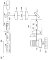
- the exposure apparatus 200 is an apparatus that exposes the base resist layer.
- the exposure apparatus 200 includes a laser light source 201, a first mirror 203, a photodiode (PD) 205, a deflection optical system, a control mechanism 230, a second mirror 213, a moving optical table 220, and a spindle motor. 225 and a turntable 227. Further, the master base material 110 is placed on the turntable 227 and can rotate.
- the laser light source 201 is a light source that emits laser light 200A, and is, for example, a solid-state laser or a semiconductor laser.
- the wavelength of the laser light 200A emitted from the laser light source 201 is not particularly limited, but may be, for example, a blue light band wavelength of 400 nm to 500 nm.
- the spot diameter of the laser beam 200A (the diameter of the spot irradiated on the resist layer) may be smaller than the diameter of the opening surface of the concave portion of the master concavo-convex structure 120, for example, about 200 nm.
- the laser beam 200 ⁇ / b> A emitted from the laser light source 201 is controlled by the control mechanism 230.
- the laser beam 200A emitted from the laser light source 201 travels straight in a parallel beam, is reflected by the first mirror 203, and is guided to the deflection optical system.
- the first mirror 203 is composed of a polarization beam splitter, and has a function of reflecting one of the polarization components and transmitting the other of the polarization components.
- the polarization component transmitted through the first mirror 203 is received by the photodiode 205 and subjected to photoelectric conversion.
- the light reception signal photoelectrically converted by the photodiode 205 is input to the laser light source 201, and the laser light source 201 performs phase modulation of the laser light 200A based on the input light reception signal.
- the deflection optical system includes a condenser lens 207, an electro-optic deflector (EOD) 209, and a collimator lens 211.
- EOD electro-optic deflector
- the laser beam 200A is condensed on the electro-optic deflection element 209 by the condenser lens 207.
- the electro-optic deflection element 209 is an element that can control the irradiation position of the laser light 200A.
- the exposure apparatus 200 can also change the irradiation position of the laser beam 200A guided onto the moving optical table 220 by the electro-optic deflection element 209 (so-called wobble mechanism).
- the laser beam 200 ⁇ / b> A is converted into a parallel beam again by the collimator lens 211 after the irradiation position is adjusted by the electro-optic deflection element 209.
- the laser light 200 ⁇ / b> A emitted from the deflection optical system is reflected by the second mirror 213 and guided horizontally and parallel onto the moving optical table 220.
- the moving optical table 220 includes a beam expander (BEX) 221 and an objective lens 223.
- the laser beam 200 ⁇ / b> A guided to the moving optical table 220 is shaped into a desired beam shape by the beam expander 221, and then irradiated to the substrate resist layer formed on the master substrate 110 through the objective lens 223. Is done. Further, the moving optical table 220 moves by one feed pitch (track pitch) in the arrow R direction (feed pitch direction) every time the master base 110 rotates once.
- the master base material 110 is installed on the turntable 227.
- the spindle motor 225 rotates the master base 110 by rotating the turntable 227. Thereby, the laser beam 200A is scanned on the base resist layer.
- a latent image of the base material resist layer is formed along the scanning direction of the laser beam 200A. Accordingly, the track direction (that is, the arrow B direction) of the first micro concavo-convex structure 11 and the second micro concavo-convex structure 12 corresponds to the scanning direction of the laser light 200A.
- the control mechanism 230 includes a formatter 231 and a driver 233, and controls the irradiation with the laser light 200A.
- the formatter 231 generates a modulation signal for controlling the irradiation of the laser light 200A, and the driver 233 controls the laser light source 201 based on the modulation signal generated by the formatter 231. Thereby, irradiation of the laser beam 200A to the master base material 110 is controlled.
- the formatter 231 generates a control signal for irradiating the substrate resist layer with the laser light 200A based on an input image on which an arbitrary pattern drawn on the substrate resist layer is drawn. Specifically, first, the formatter 231 acquires an input image on which an arbitrary pattern to be drawn on the base material resist layer is drawn. The input image is an image corresponding to a developed view of the outer peripheral surface of the base resist layer, which has been cut open in the axial direction and extended to one plane. Next, the formatter 231 divides the input image into small areas of a predetermined size (for example, in a grid pattern), and determines whether each small area includes a drawing pattern.
- a predetermined size for example, in a grid pattern
- the formatter 231 generates a control signal that controls to irradiate the laser light 200 ⁇ / b> A to each small region that is determined to include a drawing pattern.
- the control signal (that is, the exposure signal) is preferably synchronized with the rotation of the spindle motor 225, but may not be synchronized. Further, the synchronization between the control signal and the rotation of the spindle motor 225 may be reset every time the master base material 110 rotates once.
- the driver 233 controls the output of the laser light source 201 based on the control signal generated by the formatter 231. Thereby, irradiation of the laser beam 200A to the base resist layer is controlled.
- the exposure apparatus 200 may perform known exposure control processing such as focus servo, position correction of the irradiation spot of the laser beam 200A, and the like.
- the focus servo may use the wavelength of the laser beam 200A, or may use another wavelength for reference.
- the laser beam 200A irradiated from the laser light source 201 may be irradiated to the base resist layer after being branched into a plurality of optical systems. In this case, a plurality of irradiation spots are formed on the base resist layer. In this case, the exposure may be terminated when the laser beam 200A emitted from one optical system reaches the latent image formed by the other optical system.
- the transfer device 300 includes a micro uneven master 100, a substrate supply roll 301, a winding roll 302, guide rolls 303 and 304, a nip roll 305, a peeling roll 306, a coating apparatus 307, and a light source 309. Prepare.
- the base material supply roll 301 is a roll in which the long base material 10 is wound in a roll shape
- the winding roll 302 is a roll that winds up the base material 10 on which the first micro uneven structure is formed.
- the guide rolls 303 and 304 are rolls that transport the base material 10.
- the nip roll 305 is a roll for bringing the base material 10 on which the uncured resin layer 310 is laminated, that is, the transferred film 3a into close contact with the master plate 100 for micro unevenness.
- the peeling roll 306 is a roll for peeling the base material 10 on which the first micro uneven structure 11 is formed from the micro uneven surface master 100.
- the coating device 307 includes coating means such as a coater, and applies an uncured photocurable resin composition to the substrate 10 to form an uncured resin layer 310.
- the kind in particular of photocurable resin composition is not restrict
- the coating device 307 may be, for example, a gravure coater, a wire bar coater, or a die coater.
- the light source 309 is a light source that emits light having a wavelength capable of curing the photocurable resin composition, and may be, for example, an ultraviolet lamp.
- the base material 10 is continuously sent out from the base material supply roll 301 through the guide roll 303.
- the uncured photocurable resin composition is applied to the delivered base material 10 by the coating device 307, and the uncured resin layer 310 is laminated on the base material 10.
- the to-be-transferred film 3a is produced.
- the transferred film 3a is brought into close contact with the master 100 for micro unevenness by a nip roll 305.
- the light source 309 cures the uncured resin layer 310 by irradiating light to the uncured resin layer 310 in close contact with the micro uneven master 100.
- the master uneven structure 120 formed on the outer peripheral surface of the micro uneven master 100 is transferred to the uncured resin layer 310.
- the first micro concavo-convex structure 11 having the inverted shape of the master concavo-convex structure 120 is formed on the substrate 10.
- the base material 10 on which the first micro concavo-convex structure 11 is formed is peeled off from the micro uneven surface master 100 by the peeling roll 306.
- the base material 10 is taken up by the take-up roll 302 via the guide roll 304.
- the micro uneven master 100 may be placed vertically or horizontally, and a mechanism for correcting the rotation angle and eccentricity of the micro uneven master 100 may be provided separately.
- an eccentric tilt mechanism may be provided in the chucking mechanism.
- the transfer film 3a is transported by roll-to-roll, while the peripheral shape of the micro uneven master 100 is transferred to the transfer film 3a.
- the first micro uneven structure 11 is formed on the substrate 10.
- the master uneven structure 120 of the micro uneven master 100 may be directly transferred onto the base 10.
- the coating device 307 and the light source 309 are unnecessary.
- a heating device is disposed upstream of the micro uneven master 100. The base material 10 is heated and softened by this heating device, and then the base material 10 is pressed against the master plate 100 for micro unevenness. Accordingly, the master uneven structure 120 formed on the peripheral surface of the micro uneven master 100 is transferred to the substrate 10. Therefore, the transfer device 300 can continuously form the first micro uneven structure 11 on the substrate 10.
- a transfer film in which the master uneven structure 120 of the micro uneven master 100 is transferred may be used as a transfer mold.
- the micro uneven master 100 may be duplicated by electroforming or thermal transfer, and this duplicate may be used as a transfer mold.
- the shape of the micro uneven master 100 need not be limited to a roll shape, and may be a flat master.
- Various processing methods such as anodization can be selected.
- FIG. 7 shows a configuration of the optical body 1-1 according to the first embodiment.
- the optical body 1-1 was produced by the following steps. First, a polymethyl methacrylate film (Technoloy manufactured by Sumika Acrylic Sales Co., Ltd.) having a thickness of 150 ⁇ m was prepared as the substrate 10-1. Next, the second micro uneven structure 12 was formed on one surface (here, the second surface 10B) of the substrate 10-1 using the transfer apparatus 300 shown in FIG.
- an ultraviolet curable acrylic resin composition (SK1120 manufactured by Dexerials) was used as the photocurable resin composition.
- the second surface 10B of the substrate 10-1 was previously primed in order to improve the adhesion between the substrate 10-1 and the cured layer of the uncured resin layer.
- a primer layer having a thickness of about 3 ⁇ m was formed on the second surface 10B of the substrate 10-1 by the primer treatment. Specifically, the primer treatment was performed by applying and drying a polycarbonate resin.
- the second micro uneven structures 12 were arranged in a staggered pattern.
- the dot pitch P1 was 230 nm and the track pitch P2 was 153 nm.
- the average height of the second micro-projections 12a was 250 nm.
- the substrate 10-1 was a long rectangular film.
- the dot arrangement direction L20 was parallel to the longitudinal direction of the substrate 10-1, and the intersecting arrangement direction L22 was inclined by about 40 ° with respect to a straight line perpendicular to the dot arrangement direction L20.
- An SEM photograph of the cross-sectional shape of the second micro uneven structure 12 is shown in FIG.
- a planar SEM photograph is shown in FIG.
- the master macro convex portion was a convex portion extending in the short direction of the macro concave / convex master disc, the pitch (distance between the vertices of the master macro convex portion) was 100 ⁇ m, and the height was 10 ⁇ m.
- the apex angle was 90 °. Therefore, the angle formed by the slope of the master macro convex portion and the plane between the master macro convex portions (that is, the bottom surface of the master macro concave portion) is 45 °.
- the master macro convex portion was transferred to the base material 10-1 by the method described above.
- the pressure propagation medium was a viscous body, the pressure was 0.7 MPa, and the heating temperature was 180 to 220 ° C. That is, the second micro uneven structure 12 and the macro uneven structure 13 were formed so as to overlap each other on the second surface of the substrate 10-1.
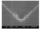
- FIG. 12 is a cross-sectional SEM photograph of the macro recess 13b. As is apparent from this photograph, it was confirmed that the second micro uneven structure 12 was formed so as to overlap on the macro recess 13b.
- the second micro convex portion 12a protrudes in the vertical direction from the surface of the macro concave portion 13b. That is, it was also confirmed that the second micro convex portion 12a was formed following the surface of the macro concave portion 13b.
- the moth-eye film 10-3 was attached to the other surface of the substrate 10-1, that is, the first surface 10A via a 25 ⁇ m thick adhesive film 10-2 (PANAC PDS1 film).
- a first micro uneven structure 11 is formed on the moth-eye film 10-3.
- the moth-eye film 10-3 was produced using the transfer device 300 described above. Specifically, a 60 ⁇ m-thick triacetyl cellulose film was used as the substrate, and an ultraviolet curable acrylic resin composition manufactured by Toagosei Co., Ltd. was used as the photo-curable resin composition.
- the thickness of the hardened layer on which the first micro uneven structure 11 is formed is about 3 ⁇ m.
- the uneven pattern of the first micro uneven structure 11 was the same as that of the second micro uneven structure 12.
- the optical body 1-1 according to Example 1 was manufactured through the above steps.
- the optical body 1-1 corresponds to the optical body 1 shown in FIG.
- spectral specular reflection spectrum was measured.
- the measurement of the regular reflection spectrum mainly evaluates the reflection characteristics of the flat portion of the optical body 1-1.
- Spectral specular reflection spectrum was measured using a spectrophotometer (model V-550, with absolute reflectance measurement unit, manufactured by JASCO Corporation). The incident angle and the reflection angle were both 5 °, the wavelength range was 400 to 800 nm, and the wavelength resolution was 1 nm. Further, the measurement light was applied to the second surface 10B. The results are shown in FIG.
- the horizontal axis in FIG. 20 indicates the measurement wavelength (nm), and the vertical axis indicates the regular reflectance (%).
- the diffuse reflection spectrum of the optical body 1-1 was measured.
- the measurement of the diffuse reflection spectrum is to evaluate the reflection characteristics on the entire surface of the optical body 1-1 including the macro uneven structure 13.
- the diffuse reflectance spectrum was measured by using the spectrophotometer (model V-550, with absolute reflectance measurement unit, manufactured by JASCO Corporation) and the absolute reflectance measuring instrument ARV474S (produced by JASCO Corporation) in combination. .
- Other conditions were the same as the measurement conditions for the specular reflection spectrum.
- a diffuse reflection spectrum is shown in FIG.
- the horizontal axis in FIG. 21 indicates the measurement wavelength (nm), and the vertical axis indicates the diffuse reflectance (%).
- a luminance meter (CS1000 manufactured by Konica Minolta Co., Ltd.) was installed on the surface 10A side of the first surface 10A, the installation position was 50 cm away from the first surface 10A, and the optical axis of the luminance meter was perpendicular to the first surface.
- High-intensity white light was incident on the optical body 1-1 from the LED light source, and the luminance (cd / cm 2 ) and xy value were measured with a luminance meter, which is perpendicular to the propagation direction L of the internal propagation light in Example 1.
- the angle formed between the straight line L21 and the intersecting arrangement direction L22 is 40 °, and the results are shown in Table 1.
- FIG. 8 shows a configuration of the optical body 1-2 according to the second embodiment.
- the optical body 1-2 was produced by using the optical body 1-1 as a transfer mold. Specifically, first, the base material 10-1 used in Example 1 was prepared. Subsequently, in order to improve the adhesion between the substrate 10-1 and each cured layer described later, both surfaces of the substrate 10-1 were subjected to primer treatment. The specific content of the primer treatment was the same as in Example 1. A primer layer having a thickness of about 3 ⁇ m was formed on both surfaces of the substrate 10-1 by the primer treatment. Next, an uncured resin layer of the photocurable resin composition was formed on one surface (here, the second surface 10B) of the substrate 10-1.
- the shape of the second surface 10B of the optical body 1-1 that is, the second micro uneven structure 12 and the macro uneven structure 13 were transferred to the uncured resin layer.
- the first macro uneven cured layer 10-5 was formed on the second surface 10B of the base material 10-1.
- the thickness of the first macro uneven cured layer 10-5 was about 3 ⁇ m.
- a second micro uneven structure 12 and a macro uneven structure 13 are formed in the first macro uneven cured layer 10-5.
- these 2nd micro uneven structure 12 and the macro uneven structure 13 have the reverse shape of the 2nd micro uneven structure 12 and the macro uneven structure 13 of Example 1.
- an uncured resin layer of the photocurable resin composition was formed on the other surface of the substrate 10-1, that is, the first surface 10A.
- the shape of the first surface 10A of the optical body 1-1, that is, the first micro uneven structure 11 was transferred to the uncured resin layer.
- a first micro uneven hardened layer 10-6 was formed on the first surface 10A of the substrate 10-1.
- the thickness of the first micro concave-convex cured layer 10-6 was about 3 ⁇ m.
- a first micro uneven structure 11 is formed in the first micro uneven cured layer 10-6.
- the first micro uneven structure 11 has an inverted shape of the first micro uneven structure 11 of the first embodiment.
- the optical body 1-2 according to Example 2 was manufactured through the above steps.
- the optical body 1-2 corresponds to the optical body 1A shown in FIG.
- Example 2 (2-2. Characteristic evaluation) Subsequently, the characteristics of the optical body 1-2 were evaluated in the same manner as in Example 1. A regular reflection spectrum is shown in FIG. 20, and a diffuse reflection spectrum is shown in FIG. In addition, Table 1 shows luminance and xy values. Further, Table 2 shows luminous reflectance and reflection chromaticity a * , b * .
- FIG. 9 illustrates a configuration of the optical body 1-3 according to the third embodiment.
- the optical body 1-3 was produced by using the optical body 1-2 as a transfer mold. Specifically, first, the base material 10-1 used in Example 1 was prepared. Subsequently, in order to improve the adhesion between the substrate 10-1 and each cured layer described later, both surfaces of the substrate 10-1 were subjected to primer treatment. The specific content of the primer treatment was the same as in Example 1. A primer layer having a thickness of about 3 ⁇ m was formed on both surfaces of the substrate 10-1 by the primer treatment.
- an uncured resin layer of the photocurable resin composition was formed on one surface (here, the second surface 10B) of the substrate 10-1.
- the shape of the second surface 10B of the optical body 1-2 that is, the second micro uneven structure 12 and the macro uneven structure 13 were transferred to the uncured resin layer.
- the second macro uneven cured layer 10-8 was formed on the second surface 10B of the base material 10-1.
- the thickness of the second macro uneven cured layer 10-8 was about 3 ⁇ m.
- a second micro uneven structure 12 and a macro uneven structure 13 are formed in the second macro uneven cured layer 10-8.
- these 2nd micro uneven structure 12 and the macro uneven structure 13 have the reverse shape of the 2nd micro uneven structure 12 and the macro uneven structure 13 of Example 2.
- FIG. That is, the second micro uneven structure 12 and the macro uneven structure 13 of Example 3 have substantially the same shape as the second micro uneven structure 12 and macro uneven structure 13 of Example 1.
- an uncured resin layer of the photocurable resin composition was formed on the other surface of the substrate 10-1, that is, the first surface 10A.
- the shape of the first surface 10A of the optical body 1-2 that is, the first micro uneven structure 11 was transferred to the uncured resin layer.
- a second micro uneven hardened layer 10-9 was formed on the first surface 10A of the base material 10-1.
- the thickness of the second micro uneven hardened layer 10-9 was about 3 ⁇ m.
- a first micro uneven structure 11 is formed in the second micro uneven cured layer 10-9.
- the first micro uneven structure 11 has an inverted shape of the first micro uneven structure 11 of the second embodiment. That is, the first micro uneven structure 11 of Example 3 has substantially the same shape as the first micro uneven structure 11 of Example 1.
- the optical body 1-3 according to Example 3 was manufactured through the above steps.
- the optical body 1-3 corresponds to the optical body 1 shown in FIG.
- Example 2 (3-2. Characteristic evaluation) Subsequently, the characteristics of the optical body 1-3 were evaluated in the same manner as in Example 1. A regular reflection spectrum is shown in FIG. 20, and a diffuse reflection spectrum is shown in FIG. In addition, Table 1 shows luminance and xy values. Further, Table 2 shows luminous reflectance and reflection chromaticity a * , b * .
- FIG. 13 shows a configuration of an optical body 500 according to Comparative Example 1.
- the optical body 500 was manufactured through the following steps. First, a substrate 510 similar to the substrate 10-1 used in Example 1 was prepared. Next, the macro uneven structure 520 was formed on the surface of the substrate 510 using the macro uneven master used in Example 1.
- the macro concavo-convex structure 520 includes a macro convex portion 520a and a macro concave portion 520b, and the macro concave portion 520b has an inverted shape of the master macro convex portion.
- the optical body 500 which concerns on the comparative example 1 was produced according to the above process.
- Example 2 (4-2. Characteristic evaluation) Subsequently, the characteristic evaluation of the optical body 500 was performed in the same manner as in Example 1. A regular reflection spectrum is shown in FIG. 20, and a diffuse reflection spectrum is shown in FIG. In addition, Table 1 shows luminance and xy values. Further, Table 2 shows luminous reflectance and reflection chromaticity a * , b * .
- FIG. 14 shows a configuration of an optical body 600 according to Comparative Example 2.
- the optical body 600 was produced by attaching the moth-eye film 620 to the back surface of the optical body 500 (that is, the surface on the side where the macro uneven structure 520 is not formed) via the adhesive film 610.
- the adhesive film 610 and the moth-eye film 620 were the same as the adhesive film 10-2 and the moth-eye film 10-3 used in Example 1.
- Example 2 (5-2. Characteristic evaluation) Subsequently, the characteristic evaluation of the optical body 600 was performed in the same manner as in Example 1. A regular reflection spectrum is shown in FIG. 20, and a diffuse reflection spectrum is shown in FIG. In addition, Table 1 shows luminance and xy values. Further, Table 2 shows luminous reflectance and reflection chromaticity a * , b * .
- FIG. 15 shows a configuration of an optical body 700 according to Comparative Example 3.
- an optical body 700 was manufactured by attaching an antireflection film 720 having a thickness of 60 ⁇ m to both surfaces of the optical body 500 via an adhesive film 710.
- the adhesive film 610 was the same as the adhesive film 10-2 used in Example 1.
- the antireflection film 720 was an AR film of inorganic four-layer film manufactured by Dexerials.
- Example 2 (5-2. Characteristic evaluation) Subsequently, the characteristic evaluation of the optical body 600 was performed in the same manner as in Example 1. A regular reflection spectrum is shown in FIG. 20, and a diffuse reflection spectrum is shown in FIG. In addition, Table 1 shows luminance and xy values. Further, Table 2 shows luminous reflectance and reflection chromaticity a * , b * .
- Example 2 the luminance in Examples 1 and 3 was superior to that in Example 2.
- the macro concave portion 13b which is a reflection portion of the internally propagating light is engraved in the optical bodies 1-1 and 1-3. For this reason, much of the internally propagating light traveling in the direction perpendicular to the thickness direction of the optical bodies 1-1 and 1-3, that is, so-called parallel light hits the film and the recess 13b and is totally reflected.
- the macro convex portion 13a which is a reflection portion of the internally propagating light, projects outward in the thickness direction of the optical body 1-2. For this reason, it becomes difficult for the parallel light to hit the macro convex portion 13a. For this reason, it is considered that the luminance in Examples 1 and 3 was superior to that in Example 2.
- an optical body 1-1A obtained by removing the macro uneven structure 13 from the optical body 1-1 described above was prepared as an optical body corresponding to the present embodiment.
- This optical body 1-1A was produced by removing the process of the master plate for macro unevenness from the process of producing the optical body 1-1.
- a comparative optical body Comparative Example 4
- optical body 1-1B such an optical body is also referred to as “optical body 1-1B”).
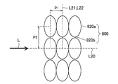
- the micro concavo-convex structure 800 has a large number of micro convex portions 800a and micro concave portions 800b.
- the optical body 1-1B was produced by changing the master uneven structure 120 of the master 100 for micro unevenness of the transfer device 300.
- the dot pitch P1, the track pitch P2, and the average height of the micro concavo-convex structure 800 were the same as those of the first micro concavo-convex structure 11 and the second micro concavo-convex structure 12 of Example 1.
- the arrangement was a lattice arrangement, and the dot arrangement direction L20 was a direction parallel to the longitudinal direction of the optical body 1-1B.
- a planar SEM photograph of the micro uneven structure 800 is shown in FIG.
- optical body 1-1D having a micro concavo-convex structure arranged in the above is prepared.
- Such a micro uneven structure was produced by changing the master uneven structure 120 of the micro uneven master 100 of the transfer device 300.
- the master plate 100 for micro unevenness was produced by randomly changing the irradiation interval of the laser light 200 ⁇ / b> A when performing exposure using the exposure apparatus 200.
- the average period of the micro concavo-convex structure was 200 nm.
- the same experiment as the above-described measurement of luminance and xy value was performed.
- the angle formed by the straight line L21 perpendicular to the propagation direction L of the internal propagation light and the intersecting arrangement direction L22 is 40 °.
- the angle formed by the straight line L21 perpendicular to the propagation direction L of the internal propagation light and the intersecting arrangement direction L22 is 0 °.
- the arrangement direction cannot be defined.
- the luminance of the optical body 1-1A is 8.5 cd / m 2
- the luminance of the optical body 1-1B is 9.2 cd / m 2
- the luminance of the optical body 1-1C is 12.3 cd / m 2. 2 .
- a similar experiment was performed by further setting the position of the LED light source on the side surface on the longitudinal side of the optical body 1-1B.
- the wave 17 shows the correspondence between the propagation direction L at this time, the dot arrangement direction L20, and the cross arrangement direction L22. Even in this case, the angle formed by the straight line L21 perpendicular to the propagation direction L of the internal propagation light and the intersecting arrangement direction L22 is 0 °.
- the luminance of the optical body 1-1B was 9.7 cd / m 2 . Therefore, the luminance of the optical body 1-1A was the smallest.
- the micro uneven structure needs to be periodically arranged, and the intersecting arrangement direction L22 is relative to the straight line L21 perpendicular to the propagation direction L of the internal propagation light. It has been found that it is necessary to incline and the angle needs to be 30-60 ° C.
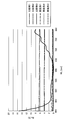
- the incident angle was changed within the range of 0 to 70 °, and the measurement wavelength was set to 380 nm to 780 nm. It was.
- the reflection angle was the same value as the incident angle.
- the same process was performed by changing the average height of the first micro uneven structure 11 (specifically, the average height of the first micro protrusion 11a).
- the luminous reflectance (that is, the Y value in the Yxy color space) was measured. The results are shown in FIG.
- the horizontal axis in FIG. 22 indicates the incident angle of the measurement light, and the vertical axis indicates the luminous reflectance (reflection Y value).
- a small luminous reflectance in this range means that the luminous reflectance on the macro uneven structure 13 is also small. In this respect, it was found that the luminous reflectance is sufficiently small when the average height is 200 nm or more.
Landscapes
- Physics & Mathematics (AREA)
- General Physics & Mathematics (AREA)
- Optics & Photonics (AREA)
- Engineering & Computer Science (AREA)
- Manufacturing & Machinery (AREA)
- Planar Illumination Modules (AREA)
- Surface Treatment Of Optical Elements (AREA)
- Light Guides In General And Applications Therefor (AREA)
- Liquid Crystal (AREA)
Priority Applications (4)
| Application Number | Priority Date | Filing Date | Title |
|---|---|---|---|
| US16/077,800 US11971569B2 (en) | 2016-03-25 | 2017-03-23 | Optical body and light emitting device |
| EP17770349.3A EP3428694B1 (en) | 2016-03-25 | 2017-03-23 | Optical body and light-emitting device |
| PL17770349.3T PL3428694T3 (pl) | 2016-03-25 | 2017-03-23 | Korpus optyczny oraz urządzenie emitujące światło |
| CN201780019295.9A CN108885284B (zh) | 2016-03-25 | 2017-03-23 | 光学体以及发光装置 |
Applications Claiming Priority (2)
| Application Number | Priority Date | Filing Date | Title |
|---|---|---|---|
| JP2016-062290 | 2016-03-25 | ||
| JP2016062290A JP6737613B2 (ja) | 2016-03-25 | 2016-03-25 | 光学体及び発光装置 |
Publications (1)
| Publication Number | Publication Date |
|---|---|
| WO2017164309A1 true WO2017164309A1 (ja) | 2017-09-28 |
Family
ID=59900257
Family Applications (1)
| Application Number | Title | Priority Date | Filing Date |
|---|---|---|---|
| PCT/JP2017/011729 Ceased WO2017164309A1 (ja) | 2016-03-25 | 2017-03-23 | 光学体及び発光装置 |
Country Status (7)
| Country | Link |
|---|---|
| US (1) | US11971569B2 (pl) |
| EP (1) | EP3428694B1 (pl) |
| JP (1) | JP6737613B2 (pl) |
| CN (1) | CN108885284B (pl) |
| HU (1) | HUE063422T2 (pl) |
| PL (1) | PL3428694T3 (pl) |
| WO (1) | WO2017164309A1 (pl) |
Cited By (1)
| Publication number | Priority date | Publication date | Assignee | Title |
|---|---|---|---|---|
| CN110109224A (zh) * | 2019-05-14 | 2019-08-09 | 深圳技术大学 | 一种基于导光板的激光阵列无线能量传输系统 |
Families Citing this family (9)
| Publication number | Priority date | Publication date | Assignee | Title |
|---|---|---|---|---|
| JP7202774B2 (ja) * | 2017-09-29 | 2023-01-12 | デクセリアルズ株式会社 | 光学体、光学体の製造方法、及び発光装置 |
| EP3776027B1 (en) * | 2018-04-02 | 2025-05-28 | Magic Leap, Inc. | Waveguides with integrated optical elements |
| JP2019188898A (ja) * | 2018-04-20 | 2019-10-31 | 矢崎総業株式会社 | 車両表示器用カバーおよび車両表示装置 |
| JP2021154626A (ja) * | 2020-03-27 | 2021-10-07 | デクセリアルズ株式会社 | 原盤の製造方法、原盤、転写物および物品 |
| KR102272612B1 (ko) * | 2021-02-08 | 2021-07-05 | 주식회사 멤스룩스 | 출광 부재와 이의 제조 방법 및 이를 포함하는 라이트 유닛 |
| CN114545539A (zh) | 2020-11-11 | 2022-05-27 | 梅姆斯莱克斯 | 出光部件和其制造方法及包含其的照明单元 |
| CN113156567B (zh) * | 2021-02-07 | 2022-09-02 | 捷开通讯(深圳)有限公司 | 导光板和显示装置 |
| US20250341670A1 (en) * | 2022-05-30 | 2025-11-06 | Carl Zeiss Jena Gmbh | Optical waveguide with a layer for reducing reflection and retardance |
| US12124074B1 (en) * | 2023-04-05 | 2024-10-22 | TieJun Wang | Light diffusing plate |
Citations (6)
| Publication number | Priority date | Publication date | Assignee | Title |
|---|---|---|---|---|
| JP2003249110A (ja) | 2001-12-21 | 2003-09-05 | Matsushita Electric Works Ltd | エッジライトパネル |
| JP2005208108A (ja) * | 2004-01-20 | 2005-08-04 | Omron Corp | 両面画像表示装置及び面光源装置 |
| JP2006012854A (ja) | 2003-10-06 | 2006-01-12 | Omron Corp | 面光源装置及び表示装置 |
| WO2006059686A1 (ja) | 2004-12-03 | 2006-06-08 | Sharp Kabushiki Kaisha | 反射防止材、光学素子、および表示装置ならびにスタンパの製造方法およびスタンパを用いた反射防止材の製造方法 |
| JP2007115438A (ja) * | 2005-10-18 | 2007-05-10 | Alps Electric Co Ltd | 導光部材、面発光装置及び発光センサ装置 |
| JP2008299079A (ja) | 2007-05-31 | 2008-12-11 | Fujikura Ltd | 表示装置 |
Family Cites Families (14)
| Publication number | Priority date | Publication date | Assignee | Title |
|---|---|---|---|---|
| JPH06342159A (ja) | 1993-05-14 | 1994-12-13 | Satoshi Inoue | 面状光源体および面状光源体の製造方法 |
| DE19708776C1 (de) * | 1997-03-04 | 1998-06-18 | Fraunhofer Ges Forschung | Entspiegelungsschicht sowie Verfahren zur Herstellung derselben |
| TWI251104B (en) * | 2004-06-07 | 2006-03-11 | Nano Prec Corp | Back lighting apparatus |
| JP2008159274A (ja) | 2006-12-20 | 2008-07-10 | Seiko Epson Corp | 導光板、導光板成形用金型、導光板成型用金型の製造方法及び導光板の製造方法 |
| US7633045B2 (en) * | 2006-08-21 | 2009-12-15 | Sony Corporation | Optical device, method for producing master for use in producing optical device, and photoelectric conversion apparatus |
| US20080158476A1 (en) * | 2006-12-06 | 2008-07-03 | Citizen Electronics Co., Ltd. | Optical member, backlight unit and display apparatus having the same |
| RU2429514C1 (ru) | 2007-08-09 | 2011-09-20 | Шарп Кабусики Кайся | Жидкокристаллическое устройство отображения |
| US8154688B2 (en) * | 2008-05-26 | 2012-04-10 | Citizen Electronics Co., Ltd. | Planar light-emitting device and liquid crystal display apparatus |
| BRPI0904808A2 (pt) * | 2008-07-16 | 2015-06-30 | Sony Corp | Elemento óptico, e, dispositivo de exibição |
| JP5527711B2 (ja) | 2010-02-25 | 2014-06-25 | 三菱レイヨン株式会社 | 面光源装置及びそれに用いる導光体 |
| WO2011125367A1 (ja) * | 2010-04-06 | 2011-10-13 | シャープ株式会社 | 光学素子、反射防止構造体及びその製造方法 |
| JP5321767B1 (ja) * | 2011-09-29 | 2013-10-23 | 凸版印刷株式会社 | 照明装置、表示装置 |
| JP6059695B2 (ja) * | 2014-09-01 | 2017-01-11 | デクセリアルズ株式会社 | 光学体の製造方法 |
| US10027846B2 (en) * | 2015-02-20 | 2018-07-17 | Mitsubishi Electric Corporation | Light guide body, light source device and image reading device |
-
2016
- 2016-03-25 JP JP2016062290A patent/JP6737613B2/ja active Active
-
2017
- 2017-03-23 PL PL17770349.3T patent/PL3428694T3/pl unknown
- 2017-03-23 WO PCT/JP2017/011729 patent/WO2017164309A1/ja not_active Ceased
- 2017-03-23 HU HUE17770349A patent/HUE063422T2/hu unknown
- 2017-03-23 US US16/077,800 patent/US11971569B2/en active Active
- 2017-03-23 CN CN201780019295.9A patent/CN108885284B/zh active Active
- 2017-03-23 EP EP17770349.3A patent/EP3428694B1/en active Active
Patent Citations (6)
| Publication number | Priority date | Publication date | Assignee | Title |
|---|---|---|---|---|
| JP2003249110A (ja) | 2001-12-21 | 2003-09-05 | Matsushita Electric Works Ltd | エッジライトパネル |
| JP2006012854A (ja) | 2003-10-06 | 2006-01-12 | Omron Corp | 面光源装置及び表示装置 |
| JP2005208108A (ja) * | 2004-01-20 | 2005-08-04 | Omron Corp | 両面画像表示装置及び面光源装置 |
| WO2006059686A1 (ja) | 2004-12-03 | 2006-06-08 | Sharp Kabushiki Kaisha | 反射防止材、光学素子、および表示装置ならびにスタンパの製造方法およびスタンパを用いた反射防止材の製造方法 |
| JP2007115438A (ja) * | 2005-10-18 | 2007-05-10 | Alps Electric Co Ltd | 導光部材、面発光装置及び発光センサ装置 |
| JP2008299079A (ja) | 2007-05-31 | 2008-12-11 | Fujikura Ltd | 表示装置 |
Non-Patent Citations (1)
| Title |
|---|
| See also references of EP3428694A4 |
Cited By (1)
| Publication number | Priority date | Publication date | Assignee | Title |
|---|---|---|---|---|
| CN110109224A (zh) * | 2019-05-14 | 2019-08-09 | 深圳技术大学 | 一种基于导光板的激光阵列无线能量传输系统 |
Also Published As
| Publication number | Publication date |
|---|---|
| EP3428694A4 (en) | 2019-10-30 |
| CN108885284A (zh) | 2018-11-23 |
| US20210191024A1 (en) | 2021-06-24 |
| PL3428694T3 (pl) | 2023-12-04 |
| HUE063422T2 (hu) | 2024-01-28 |
| CN108885284B (zh) | 2021-06-25 |
| US11971569B2 (en) | 2024-04-30 |
| JP2017173733A (ja) | 2017-09-28 |
| EP3428694A1 (en) | 2019-01-16 |
| EP3428694B1 (en) | 2023-07-26 |
| JP6737613B2 (ja) | 2020-08-12 |
Similar Documents
| Publication | Publication Date | Title |
|---|---|---|
| JP6737613B2 (ja) | 光学体及び発光装置 | |
| US8027090B2 (en) | Optical element, replica substrate configured to form optical element | |
| JP7282496B2 (ja) | 光学体、光学体の製造方法、発光装置及び遊戯機器用表示装置 | |
| CN107111002A (zh) | 光学体、光学膜粘合体及光学体的制造方法 | |
| WO2022071397A1 (ja) | 光学フィルムおよび光学フィルムの製造方法 | |
| WO2010074191A1 (ja) | 光学素子、表示装置、反射防止機能付き光学部品、および原盤 | |
| JP2013254130A (ja) | 光学素子およびその製造方法、表示素子、ならびに投射型画像表示装置 | |
| WO2015194649A1 (ja) | 光学体、フィルム貼付体、及び光学体の製造方法 | |
| US10732341B2 (en) | Optical body, method for manufacturing optical body, and light-emitting apparatus | |
| US20050128582A1 (en) | Display screen and its method of production | |
| JP2019066644A (ja) | 光学体及び発光装置 | |
| JP6107131B2 (ja) | ナノ構造体及びその作製方法 | |
| TW201622968A (zh) | 壓紋膜、單張膜、轉寫物、及壓紋膜之製造方法 | |
| WO2011162165A1 (ja) | 光拡散フィルムの製造方法、および当該製造方法によって製造された光拡散フィルム、ならびに当該光拡散フィルムを備えた表示装置 | |
| US10883676B2 (en) | Optical body having a concave-convex structure, method for manufacturing the optical body, and light emitting device |
Legal Events
| Date | Code | Title | Description |
|---|---|---|---|
| NENP | Non-entry into the national phase |
Ref country code: DE |
|
| WWE | Wipo information: entry into national phase |
Ref document number: 2017770349 Country of ref document: EP |
|
| ENP | Entry into the national phase |
Ref document number: 2017770349 Country of ref document: EP Effective date: 20181011 |
|
| 121 | Ep: the epo has been informed by wipo that ep was designated in this application |
Ref document number: 17770349 Country of ref document: EP Kind code of ref document: A1 |