WO2017164403A1 - Stratifié sensible aux ondes électromagnétiques - Google Patents
Stratifié sensible aux ondes électromagnétiques Download PDFInfo
- Publication number
- WO2017164403A1 WO2017164403A1 PCT/JP2017/012145 JP2017012145W WO2017164403A1 WO 2017164403 A1 WO2017164403 A1 WO 2017164403A1 JP 2017012145 W JP2017012145 W JP 2017012145W WO 2017164403 A1 WO2017164403 A1 WO 2017164403A1
- Authority
- WO
- WIPO (PCT)
- Prior art keywords
- electromagnetic wave
- particles
- protective member
- specific wavelength
- shape
- Prior art date
- Legal status (The legal status is an assumption and is not a legal conclusion. Google has not performed a legal analysis and makes no representation as to the accuracy of the status listed.)
- Ceased
Links
Images




Classifications
-
- B—PERFORMING OPERATIONS; TRANSPORTING
- B32—LAYERED PRODUCTS
- B32B—LAYERED PRODUCTS, i.e. PRODUCTS BUILT-UP OF STRATA OF FLAT OR NON-FLAT, e.g. CELLULAR OR HONEYCOMB, FORM
- B32B3/00—Layered products comprising a layer with external or internal discontinuities or unevennesses, or a layer of non-planar shape; Layered products comprising a layer having particular features of form
- B32B3/10—Layered products comprising a layer with external or internal discontinuities or unevennesses, or a layer of non-planar shape; Layered products comprising a layer having particular features of form characterised by a discontinuous layer, i.e. formed of separate pieces of material
- B32B3/18—Layered products comprising a layer with external or internal discontinuities or unevennesses, or a layer of non-planar shape; Layered products comprising a layer having particular features of form characterised by a discontinuous layer, i.e. formed of separate pieces of material characterised by an internal layer formed of separate pieces of material which are juxtaposed side-by-side
- B32B3/22—Layered products comprising a layer with external or internal discontinuities or unevennesses, or a layer of non-planar shape; Layered products comprising a layer having particular features of form characterised by a discontinuous layer, i.e. formed of separate pieces of material characterised by an internal layer formed of separate pieces of material which are juxtaposed side-by-side of spaced pieces
-
- B—PERFORMING OPERATIONS; TRANSPORTING
- B41—PRINTING; LINING MACHINES; TYPEWRITERS; STAMPS
- B41M—PRINTING, DUPLICATING, MARKING, OR COPYING PROCESSES; COLOUR PRINTING
- B41M3/00—Printing processes to produce particular kinds of printed work, e.g. patterns
- B41M3/14—Security printing
Definitions
- the present invention relates to an electromagnetic wave responsive laminate that can be easily imparted with designability, anti-counterfeiting properties, etc., and is excellent in durability.
- Non-Patent Document 1 discloses a laminate in which silver nanocube particles are fixed to the surface of a transparent substrate as particles capable of scattering visible light by plasmon resonance. Further, in Non-Patent Document 1, the wavelength of visible light that causes plasmon resonance is different between the surface of the particle on the substrate side and the surface opposite to the substrate. It is shown that images of different colors can be displayed depending on whether the side is opposite to the substrate.
- the laminate having particles dispersed on the surface of the substrate can be used as an electromagnetic wave-responsive laminate that responds to electromagnetic waves of a specific wavelength. And anti-counterfeiting properties may be imparted to the laminate.
- the particles dispersed on the surface of the base material are exposed and fixed to the atmosphere, for example, when the user's hand touches the particles, the particles may fall off and not exhibit the desired function. There is sex.
- an overcoat layer that covers the particles in contact with the particle surface in order to prevent the particles from falling off.
- electromagnetic wave responsiveness specifically, photoresponsiveness may not be exhibited effectively. This is because it is considered that the photoresponsiveness of the particles to the light having the specific wavelength is greatly influenced by the difference in refractive index on the particle surface. For this reason, when the overcoat layer is formed so as to be in contact with the particle surface, there is a possibility that the wavelength of light exhibiting photoresponsiveness changes as compared with the case where the particle surface is exposed and is in contact with air.
- the laminated body has a problem that, for example, an image of a specific color cannot be displayed.
- the laminate disclosed in Non-Patent Document 1 when an overcoat layer in contact with the particle surface is formed, the refractive index difference between the particle opposite to the substrate (the difference between the particle and the overcoat layer). The difference between the refractive index difference) and the refractive index difference between the particles on the substrate side surface (refractive index difference between the particles and the substrate), that is, the difference in refractive index between the front and back surfaces of the particles is reduced.
- the wavelength of the plasmon-resonant light on the material side surface and the surface opposite to the base material is close. Thereby, it is difficult for the laminate of Non-Patent Document 1 to scatter light of different wavelengths on the front and back, and as a result, it may be difficult to display images of different colors on the front and back.
- the present invention has been made in view of the above problems, and has as its main object to provide an electromagnetic wave responsive laminate that is easy to impart designability, anti-counterfeiting properties, etc., and is excellent in durability. To do.
- the present invention protects a base material, particles fixed on one surface of the base material in an exposed state and having electromagnetic wave response to an electromagnetic wave having a specific wavelength, and the particles.
- a protective member, and the protective member is disposed on the same surface side as the surface of the substrate on which the particles are fixed, and is a member having a height higher than that of the particles.
- a laminate is provided.
- the electromagnetic wave response laminated body of this invention has an electromagnetic wave response with respect to the electromagnetic wave of a specific wavelength.
- the electromagnetic wave-responsive laminate of the present invention can effectively exhibit the electromagnetic wave response of the particles.
- the electromagnetic wave responsive laminated body of this invention can prevent that a particle
- the particles are preferably made of a negative dielectric material and capable of plasmon resonance with the electromagnetic wave having the specific wavelength, and the electromagnetic wave having the specific wavelength is preferably visible light. Since the particles are capable of plasmon resonance, and the electromagnetic wave having the specific wavelength is visible light, the electromagnetic wave-responsive laminate of the present invention can be imparted with designability and anti-counterfeiting property using plasmon resonance. Because it becomes. For example, the electromagnetic wave-responsive laminate of the present invention exhibits design properties, anti-counterfeiting properties, etc., when an electromagnetic wave having a specific wavelength scattered by plasmon resonance is displayed with a specific color when irradiated with white light. It becomes possible.
- the particles are preferably made of a dielectric material, capable of Mie scattering or Rayleigh scattering with respect to the electromagnetic wave having the specific wavelength, and the electromagnetic wave having the specific wavelength is preferably visible light. . Since the particles are capable of Mie scattering and the like, and the electromagnetic wave having the specific wavelength is visible light, the electromagnetic wave-responsive laminate of the present invention has a design property using a light scattering effect by Mie scattering or Rayleigh scattering. This is because it is possible to impart anti-counterfeiting properties and the like.
- the electromagnetic wave-responsive laminate of the present invention has a design property, anti-counterfeiting property, etc., by displaying an image of a specific color of an electromagnetic wave having a specific wavelength scattered by Mie scattering or Rayleigh scattering when irradiated with white light. Can be achieved.
- the particles are made of a dielectric material and can be Mie scattered or Rayleigh scattered with respect to the electromagnetic wave having the specific wavelength, and the electromagnetic wave having the specific wavelength is larger than the visible light. It is preferable that The particles are capable of Mie scattering or Rayleigh scattering with respect to the electromagnetic wave having the specific wavelength, and the electromagnetic wave having the specific wavelength is an electromagnetic wave having a wavelength larger than that of visible light. This is because it is possible to impart anti-counterfeiting using a light scattering effect by Mie scattering or Rayleigh scattering.
- the electromagnetic wave responsive laminate of the present invention detects the wavelength scattered by Mie scattering or Rayleigh scattering, and confirms the presence or absence of predetermined particles by confirming whether or not an electromagnetic wave having a specific wavelength is detected. be able to. Thereby, forgery prevention property can be exhibited.
- the electromagnetic wave having a specific wavelength is an electromagnetic wave having a wavelength larger than that of visible light
- the electromagnetic wave responsive laminate of the present invention is disposed inside a forgery prevention target or the like, or is irradiated with an electromagnetic wave. Attracting attention can be prevented. For this reason, it is because the electromagnetic wave response laminated body of this invention becomes the thing excellent in forgery prevention property.
- the planar view shape of the particle arrangement region is preferably a pattern shape. This is because the electromagnetic wave-responsive laminate of the present invention can be easily provided with designability and the like because the planar view shape is a pattern shape.
- a cover layer covering the particles and the protective member is not formed on one surface of the base material. It is because the electromagnetic wave responsive laminated body of this invention can exhibit the electromagnetic wave responsiveness of particle
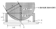
- the average primary particle size of the particles is h, the radius of curvature of the convex portion of the fingerprint of the skin to touch the electromagnetic wave responsive laminate, r, the height of the protective member a,
- the interval between the protective members is b, it is preferable to satisfy the following formula (III). It is because the said protection member can protect particle
- the present invention has an effect of providing an electromagnetic wave-responsive laminate that can be easily provided with designability, anti-counterfeiting properties, etc., and has excellent durability.
- the present invention relates to an electromagnetic wave responsive laminate.
- the electromagnetic wave responsive laminate of the present invention will be described in detail.
- the electromagnetic wave responsive laminate of the present invention includes a base material, particles fixed to one surface of the base material in an exposed state, and having electromagnetic wave response to an electromagnetic wave having a specific wavelength, and a protective member for protecting the particles.
- the protective member is arranged on the same side as the surface of the base material on which the particles are fixed, and is a member having a height higher than that of the particles.
- FIGS. 1 (a) and 1 (b) are schematic cross-sectional views showing an example of the electromagnetic wave responsive laminate of the present invention.
- the electromagnetic wave responsive laminate 10 of the present invention is fixed in an exposed state on one surface of the base material 1 and the base material 1, and is applied to an electromagnetic wave having a specific wavelength.
- the particle 2 having electromagnetic wave responsiveness and a protective member 3 for protecting the particle 2 are provided on the same surface side as the surface of the substrate 1 on which the particle 2 is fixed. It is a member which is disposed and is higher than the particle 2.
- the substrate 1 has a support substrate 1a and a high refractive index layer 1b.
- the protective member 3 may be disposed on the support base 1a and the high refractive index layer 1b, or as shown in FIG. 1 (b).
- the protective member 3 may be disposed on the support base 1a, and the high refractive index layer 1b may be disposed so as to cover the support base 1a and the protective member 3. It can select suitably according to the manufacturing method of the electromagnetic wave responsive laminated body of this invention.
- the electromagnetic wave may be anything that causes plasmon resonance, Mie scattering, Rayleigh scattering, or the like.
- ultraviolet light (10 nm or more and less than 360 nm), visible light (360 nm or more and less than 830 nm), infrared light (830 nm or more and less than 0.1 mm).
- Microwaves (0.1 mm or more and less than 1 m), short waves (1 m or more and less than 100 m), and the like.
- the electromagnetic wave response laminated body of this invention has an electromagnetic wave response with respect to the electromagnetic wave of a specific wavelength. Further, since the particles are fixed in an exposed state, at least the surface opposite to the substrate is exposed and the particles are in contact with the atmosphere. As a result, the electromagnetic wave responsive laminate of the present invention can easily adjust the electromagnetic wave responsiveness to electromagnetic waves of a specific wavelength. For example, the color of scattered light and electromagnetic waves observed when irradiated with visible light as electromagnetic waves. It becomes easy to set the wavelength or the like of the electromagnetic wave scattered when the light is irradiated to a desired color or wavelength.
- the electromagnetic wave responsive laminate of the present invention displays images of different colors when observed by irradiating visible light as electromagnetic waves from the front side and when observed by irradiating visible light as electromagnetic waves from the back side. It will be possible. As described above, the electromagnetic wave responsive laminate of the present invention can effectively exhibit the electromagnetic wave responsiveness of the particles, and can be easily provided with designability, anti-counterfeiting property, and the like.
- the electromagnetic wave responsive laminate of the present invention can prevent the particles from dropping off during use, and has excellent durability.
- the electromagnetic wave-responsive laminate of the present invention can be easily imparted with designability, anti-counterfeiting properties, etc., and has excellent durability.
- the electromagnetic wave-responsive laminate can be combined with the type of particle and the wavelength of the electromagnetic wave depending on the application.
- Examples of the combination of the type of particles and the wavelength of the electromagnetic wave of such an electromagnetic wave responsive laminate are, for example, those in which the particle is made of a negative dielectric material and can be plasmon-resonated with respect to the electromagnetic wave of the specific wavelength
- the embodiment in which the electromagnetic wave having the specific wavelength is visible light (first embodiment), and the particles are made of a dielectric material and can be Mie scattered or Rayleigh scattered with respect to the electromagnetic wave having the specific wavelength.
- the embodiment in which the electromagnetic wave having the specific wavelength is visible light (second embodiment) and the particles are made of a dielectric material, and can be Mie scattered or Rayleigh scattered with respect to the electromagnetic wave having the specific wavelength.
- an aspect in which the electromagnetic wave having the specific wavelength is an electromagnetic wave having a wavelength larger than that of visible light (third embodiment).
- the electromagnetic wave responsive laminate of the present invention will be described separately for each embodiment.
- the electromagnetic wave-responsive laminate of this aspect is the above-described electromagnetic wave-responsive laminate, wherein the particles are made of a negative dielectric material, and are capable of plasmon resonance with respect to the electromagnetic wave having the specific wavelength.
- the electromagnetic wave having a specific wavelength is visible light.
- plasmon resonance is possible with respect to an electromagnetic wave of a specific wavelength when the particle is irradiated with the electromagnetic wave, the electromagnetic wave of a specific wavelength is caused by the localized surface plasmon resonance of the particle (also called a localized surface plasmon polariton). It means that it can be scattered.
- the particle is capable of plasmon resonance with respect to electromagnetic waves having a specific wavelength
- the electromagnetic wave-responsive laminate according to this aspect has plasmon resonance because the electromagnetic waves having the specific wavelength are visible light. It is possible to impart designability, anti-counterfeiting properties, etc. using
- the electromagnetic wave-responsive laminate of this embodiment exhibits design properties, anti-counterfeiting properties, etc., when an electromagnetic wave having a specific wavelength scattered by plasmon resonance is displayed with a specific color when irradiated with white light. It becomes possible.
- the electromagnetic wave response laminated body of this aspect has a base material, particle
- each structure of the electromagnetic wave response laminated body of this aspect is demonstrated.
- the particles are fixed in an exposed state on one surface of the substrate.
- the particles are made of a negative dielectric material and are capable of plasmon resonance with visible light having the specific wavelength. Furthermore, the particles in this embodiment are so-called fine particles having a predetermined particle size.
- grains is mentioned later, description here is abbreviate
- the exposed state refers to a state in which at least the surface on the opposite side of the particle substrate is exposed and is not in contact with other members, and is usually at least the surface on the opposite side of the particle substrate. Refers to the state of contact with the atmosphere.
- the wavelength of visible light that plasmon-resonates (hereinafter sometimes simply referred to as light) is affected by the shape of the particle, the constituent material, and the like. For this reason, the wavelength of the plasmon-resonant visible light can be adjusted by adjusting the shape and constituent materials of the particles. For example, red, blue, yellow can be used as specific colors when irradiated with white light. Etc. can be scattered.
- the wavelength of light that causes plasmon resonance is preferably in the range of 360 nm to 830 nm, and preferably in the range of 400 nm to 760 nm. This is because the particles easily cause plasmon resonance when the wavelength of the light is within the above-mentioned range.
- the average primary particle diameter of the particles is not particularly limited as long as it is capable of plasmon resonance with respect to light.
- the average primary particle diameter is preferably in the range of 2 nm to 200 nm, and more preferably in the range of 5 nm to 150 nm. In particular, it is preferably in the range of 10 nm to 100 nm. This is because, when the average primary particle size is within the above range, the particles easily cause plasmon resonance.
- the said average primary particle diameter can be calculated
- a particle image was measured with a transmission electron micrograph (TEM) (for example, H-7650 manufactured by Hitachi High-Tech), and the average value of the length of the longest part of 100 or more randomly selected primary particles.
- TEM transmission electron micrograph
- the electron microscope may be either a transmission type (TEM) or a scanning type (SEM).
- the type of the average primary particle size is not limited to one using only one type, and two or more types may be used. When there are two or more types of average primary particle sizes, for example, particles having an average primary particle size in the range of 100 nm and particles having an average primary particle size of 200 nm can be mixed and used.
- the particle size distribution of the particles is not particularly limited as long as it is capable of plasmon resonance with respect to light.
- the particle size distribution is narrow from the viewpoint of displaying an image of a specific color.
- the narrow particle size distribution can be evaluated by the value of the ratio of D90 to D50 (D90 / D50) when the particle size of 50% cumulative and 90% cumulative is D50 and D90 from the fine particle side of the cumulative particle size distribution, for example.
- D90 / D50 is preferably 2 or less, and particularly preferably 1.5 or less.
- the shape of the particles is not particularly limited as long as it is capable of plasmon resonance with respect to light.
- a spherical shape or a cylindrical shape may be used. It is preferable that the shape has a corner such as a disk shape or other plate. This is because the particles are likely to cause plasmon resonance when the shape has a corner.
- the shape is a cubic shape or a rectangular parallelepiped shape. This is because the particles are likely to cause plasmon resonance and are easy to manufacture.
- the type of the shape is not limited to one using only one type, and two or more types may be used. When there are two or more types of shapes, for example, particles having a spherical shape and particles having a cubic shape can be mixed and used.
- the constituent material of the particles is a negative dielectric material, and is a material in which the real part of the dielectric constant is negative in a specific wavelength region where electromagnetic field responsiveness is desired.
- the negative dielectric material specifically, for visible light, a metal, a metal oxide, or an impurity semiconductor can be used.
- the negative dielectric material is preferably a metal. This is because the above-described constituent material is easy to perform plasmon resonance with respect to visible light.
- the metal it is preferable that they are silver, gold
- the metal oxide is not particularly limited as long as the real part of the dielectric constant is negative.
- indium tin oxide (ITO) used for forming the transparent electrode layer of JP-A-2015-194799 is used.
- An inorganic conductive material can be mentioned.
- the impurity semiconductor for example, those described in JP-A-2015-232713 can be used.
- the types of the constituent materials are not limited to those using only one type, and two or more types may be used. In the case where there are two or more kinds of constituent materials, for example, silver particles of the constituent materials and gold particles of the constituent materials can be mixed and used.
- the particles include at least negative dielectric particles composed of the negative dielectric material, and may include only the negative dielectric particles.
- the particles may have a coating layer that covers the surface of the negative dielectric particles. This is because, when the particles have a coating layer, the particles can suppress aggregation and the like.
- a resin material capable of binding to the surface of the negative dielectric particles can be used.
- PEG polyethylene glycol
- PEG derivative polyvinyl pyrrolidone
- PVP polyvinyl pyrrolidone
- citrate ion carbonate
- examples thereof include ions, ⁇ -lipoic acid, branched polyethyleneimine (BPEI), silica, silica derivatives, and dodecanethiol.
- the thickness of the coating layer may be any thickness as long as it does not significantly interfere with the plasmon resonance of the particles, but the electromagnetic wave-responsive laminate of this embodiment can easily observe images of different colors on the front side and the back side. From, for example, it can be 2 nm or less.
- the shape of the particle arrangement region in plan view may be a shape that covers the entire surface of the substrate, but from the viewpoint of providing designability and anti-counterfeiting properties, patterns such as patterns and characters
- the shape is preferred. This is because the particles can easily impart designability and the like to the electromagnetic wave-responsive laminate by being in the above-described arrangement shape.
- the pattern shape may be a dot shape, a line shape, or the like.
- the dot shape may be any shape such as a circular shape or a square shape.
- the arrangement shape can represent a symbol, a character, or the like.
- the arrangement shape may represent a character or the like using a line arrangement area, or may represent a character or the like using a dot arrangement area.
- the whole surface of a base material means all the areas
- FIG. 1A shows an example in which the planar arrangement shape of the particle arrangement region 12 covers the entire surface of the substrate 1, and FIG. 2B shows the arrangement region 12.
- An example in which the plan view shape is a star-shaped pattern shape arranged in an area not covered by the protective member of the base material 1 is shown.
- FIGS. 1A and 1B described above show examples in which the planar view shape of the arrangement region 12 is a pattern shape that covers only the region between the protective members of the base material.
- the coverage ratio of the particles in the arrangement region may be, for example, one that can scatter light having a specific wavelength with a desired intensity in the irradiated light, and is 0.1 ⁇ 10 6 particles / cm 2 to 1000 ⁇ . It can be in the range of 10 6 pieces / cm 2 .
- the interval of the particles in the arrangement region may be any as long as it can be the above-described covering ratio, and may be arranged at an equal interval with one kind of interval, but is randomly arranged.
- the interval may be two or more types.
- the particles are fixed to one surface of the substrate.
- being fixed to one surface of the base material is not limited to the case of being fixed so as to be in direct contact with the surface of the base material, but includes the case of being fixed to the surface of the base material through a binder resin or the like.
- the fixing mode may be based on adsorption of particles on the surface of the base material, or may be in close contact with the surface of the base material by a binder resin.
- a method for fixing the particles when the fixing mode is based on adsorption of particles onto the surface of the substrate, a particle dispersion containing particles and a solvent is applied onto the substrate, and the solvent is removed by drying. And the like.
- the fixing method may be a method in which a particle forming layer made of a constituent material constituting particles is formed on a substrate, and then patterned into a desired particle shape using a photolithography method or the like.
- the fixing method include a method in which a binder resin-containing one is used as the particle dispersion when the fixing mode is closely attached by a binder resin.
- the particle dispersion coating method includes various printing methods such as screen printing, gravure printing, offset printing, flexographic printing, die coating method, spray coating method, spin coating method, dip coating method, ink jet method, and microcontact. Examples thereof include a printing method and a dip pen lithography method.
- the particle forming layer may be formed by any method that can form a coating film of a negative dielectric material. For example, a sputtering method or the like can be used.
- the binder resin is not particularly limited as long as the particles can be stably adhered to the surface of the base material, and a photocurable resin such as a known thermosetting resin, ultraviolet (UV) curable resin, or electron beam (EB) curable resin.
- a photocurable resin such as a known thermosetting resin, ultraviolet (UV) curable resin, or electron beam (EB) curable resin.
- UV curable resin ultraviolet (UV) curable resin
- EB electron beam
- the protective member in this aspect protects the particles.
- the protective member is a member that is disposed on the same surface side as the surface of the base material on which the particles are fixed and is higher than the particles.
- protecting means preventing the user's finger from touching the particles when the user touches the electromagnetic wave responsive laminate.
- Shape of protective member As the shape of the protective member, for example, when the user touches the electromagnetic wave responsive laminate, the height of the user's finger does not touch the particles and the interval is protected. The particles can be protected only by the member.
- the height of such a protective member may be any as long as it is higher than the particles and the finger does not touch the particles when the user touches the electromagnetic wave responsive laminate.
- grain means that it is larger than the average primary particle diameter of the said particle
- the lower limit of the height of the protective member is, for example, 0.
- the thickness can be 3 ⁇ m or more, preferably 1 ⁇ m or more, more preferably 5 ⁇ m or more, and particularly preferably 20 ⁇ m or more. It is because the said protective member can protect particle
- the upper limit of the height is appropriately set according to the use of the electromagnetic wave-responsive laminate of this embodiment, but from the viewpoint of easy formation of the protective member, for example, 1 mm or less. Can do.
- the height is specifically indicated by a in FIGS. 1A and 1B.
- the height a of the protective member 3 can be obtained by actual measurement.
- the height a of the protection member 3 can be obtained as follows. That is, first, the distance from the surface of the high refractive index layer 1b arranged on the support substrate 1a to the surface of the high refractive index layer 1b arranged on the protective member 3, that is, FIG. The distance indicated by the symbol a ′ is obtained.
- the thickness d 1 of the high refractive index layer 1 b disposed on the support substrate 1 a tends to be thicker than the thickness d 2 of the high refractive index layer 1 b disposed on the protective member 3.
- the height a of the protective member 3 can be calculated by adding the difference between the thickness d 1 and the thickness d 2 of the high refractive index layer 1 b to the obtained distance a ′.
- these thickness can be calculated
- the electron microscope may be either a transmission type (TEM) or a scanning type (SEM).
- the interval between the protective members is such that a finger does not touch the particles when the user touches the electromagnetic wave responsive laminate.
- Such an interval can be wider than the average primary particle size of the particles.
- the upper limit of the interval is, for example, 2 mm or less. It is preferably 1 mm or less, more preferably 500 ⁇ m or less, and particularly preferably 200 ⁇ m or less. It is because the said protection member can protect particle
- the lower limit of the interval is appropriately set according to the use of the electromagnetic wave responsive laminate of this embodiment, but the viewpoint that the electromagnetic wave responsiveness of the particles can be efficiently obtained, formation of the protective member From an easy viewpoint etc., it can be set as 10 micrometers or more, for example.
- interval of the said protection member says the distance between adjacent protection members used as the shortest about each protection member.
- the planar view shape of a protection member is a shape which has the opening part mentioned later, it means the shortest thing among the distances between the protection members separated by the opening part.
- the interval is indicated by b in FIGS. 1 (a) and 1 (b).
- the average primary particle size of the particles 2 is h
- the electromagnetic wave-responsive laminate X is touched (in FIG. 3, finger skin (fingerprint
- the curvature radius of the convex portion)) is r
- the height a and the distance b are designed so as to satisfy the conditions of the following formulas (I) and (II). That is, in this aspect, it is preferable to design so as to satisfy the condition of the following formula (III) derived from the following formulas (I) and (II). It is because the said protection member can protect particle
- the distance a ′ shown in FIG. 1B can be calculated by subtracting the difference between the thickness d 1 and the thickness d 2 of the high refractive index layer 1 b from the height a of the protective member 3.
- the approximate curvature radius r of the unevenness of the fingerprint is usually about 290 ⁇ m, The minimum value can be about 180 ⁇ m.
- the curvature radius r of the unevenness of the fingerprint for example, Takashi Maeno, Daisuke Yamada, Hidenari Sato, “Mechanical Meaning of Human Fingerprint Shape”, Transactions of the Japan Society of Mechanical Engineers (C), Vol. 71, No. 701 pp. 245 -250, (2005-1).
- a combination of height and interval a combination of 106 ⁇ m or less when the height and interval are 5 ⁇ m, a combination of 6.8 ⁇ m or less when 0.1 ⁇ m, and 211 ⁇ m or less when 20 ⁇ m, respectively. It can be set as a combination.
- the type of the interval between the protective members may be arranged at an equal interval with one type of interval, but is preferably arranged at random and the interval becomes two or more types. It is because generation
- the shape of the protective member in plan view is not particularly limited as long as it exhibits strength that does not cause damage when the user uses the electromagnetic wave-responsive laminate, and may be in a dot shape, a line shape, or the like.
- the shape in plan view may be a shape having openings such as a honeycomb shape or a lattice shape, or a shape having random openings.
- 3 is a schematic plan view and a cross-sectional view showing another example of the electromagnetic wave responsive laminate of this embodiment
- FIG. 4 (b) is a cross-sectional view taken along the line AA in FIG. 4 (a).
- FIG. 4D is a cross-sectional view taken along line BB in FIG. 4C, and FIG.
- the shape in plan view is a dot shape, a line shape, and a shape having an opening.
- An example is given.
- the shape of the protective member in plan view is a dot shape as shown in FIG. 4A, the area where the particles are arranged increases, so that a large area for displaying an image of a predetermined color can be secured. . Therefore, it can be set as the electromagnetic wave response laminated body which has the more outstanding design property and forgery prevention property.
- planar view shape of a protection member is a line shape as shown in FIG.4 (b)
- the patterning at the time of forming a protection member can be performed easily. Therefore, it can be set as the electromagnetic wave responsive laminated body which can be manufactured more easily.
- shape of the protective member in plan view is a mesh having openings as shown in FIG. 4 (c)
- the occurrence of problems such as the protective member falling down is suppressed, and high-quality electromagnetic wave responsive lamination is achieved. It can be a body.
- planar view shape of the protection member in the case of a dot shape it can be a polygonal shape such as a circular shape, a triangular shape, or a quadrangular shape.
- FIG. 4A already described shows an example in which the shape of the dot-shaped protection member in plan view is a square shape.
- the size of the protective member in plan view may be any size as long as it exhibits a strength that does not damage the user when the electromagnetic wave responsive laminate is used, and can be in the range of 0.1 ⁇ m to 100 ⁇ m. It is preferably in the range of ⁇ 50 ⁇ m. This is because the protective member can stably protect particles from contact with fingers by having the size in plan view. Further, the protective member is inconspicuous because it cannot be identified with the naked eye.
- the size in plan view refers to the maximum diameter in the case of dots, the width in the short direction in the case of lines, and the shortest distance between adjacent openings in the case of having a shape with openings. . Specifically, the size in plan view is shown by c in FIGS. 1A and 1B and FIG.
- any material may be used as long as it exhibits strength that does not break when a user uses the electromagnetic wave-responsive laminate. Examples include a trapezoidal shape and a rectangular shape on the opposite side. Especially, it is preferable that the cross-sectional shape of a protective base material is a trapezoid shape with a wide base material side. Generation
- the cross-sectional shape here refers to the shape of the cut surface when the protective member is cut in the height direction.
- the protective member may be any member as long as it is arranged so as not to overlap with at least one particle fixed to the substrate surface in plan view, and may be in contact with the particle.
- the type of the protective member can be appropriately selected according to the shape in plan view and the like.
- a columnar protective member obtained by molding the constituent material of the protective member into a pattern can be used.
- a bead-shaped protective member that is dispersed and disposed on the surface of the substrate can be used.
- 1A, 1B, and 4 described above show examples in which the type of the protective member is a columnar protective member.
- a resin material such as a cured product of a photosensitive resin can be used.
- a photosensitive resin for example, an ultraviolet curable resin used for forming a protective member of a liquid crystal display device such as Japanese Patent No. 2953594 can be used.
- a method for forming the columnar protection member any method may be used as long as it is a method obtained by forming the constituent material of the protection member into a pattern. For example, the method for forming a protection member described in Japanese Patent No. 2953594 can be used.
- the forming method when the constituent material is a cured product of a photosensitive resin, a coating film of the photosensitive resin is formed on one surface of the substrate and applied through a photomask.
- An example is a method in which the film is exposed to light and the uncured photosensitive resin is removed by development.
- the forming method includes a transfer substrate having a columnar protection member disposed on the support substrate surface, and transferring the columnar protection member to the substrate by bringing the transfer substrate into contact with the substrate. You may form using a method.
- the columnar protection member is preferably bonded and fixed to the substrate surface.
- the constituent material of the bead-shaped protective member is not particularly limited as long as it has a desired strength.
- it is the same as the constituent material of a bead used as a protective member in a liquid crystal display device such as JP-A-2007-94185. be able to.
- an inorganic material such as glass or a resin material such as an acrylic resin can be used as the constituent material.
- any method may be used as long as it is a method of disposing the bead-shaped protective member on the surface of the base material, for example, applying a dispersion containing the bead-shaped protective member on the base material, A method of drying and removing the dispersion medium can be used.
- the dispersion liquid may contain particles to be described later, that is, the forming method may be a method in which the protective member and the particles are simultaneously arranged.
- the bead-shaped protective member may be disposed so as to be movable on the surface of the base material, or may be adhered and fixed to the surface of the base material.
- the protective member has a height and a distance at which the user's finger does not touch the particles when the user touches the electromagnetic wave responsive laminate, and the particles are formed only by the protective member.
- the protective member 3 may be used as a spacer that supports a cover layer 5 described later, as illustrated in FIG. In this case, as the height and interval of the protective member, if the finger touches the particles when the user touches the electromagnetic wave responsive laminate by supporting the cover layer, Good.
- the height may be, for example, at least a distance at which the near-field light of the particles is sufficiently attenuated, and can be supported at a position that is at least twice as high as the average primary particle size of the particles.
- the height is within a range of 0.16 ⁇ m to 300 ⁇ m. can do.
- the upper limit of the height is appropriately set according to the use of the electromagnetic wave responsive laminate of this embodiment.
- the interval is preferably one that can be supported without bending the cover layer, and is appropriately selected in consideration of the thickness of the cover layer and the Young's modulus of the material. More specifically, the interval can be set in the range of 10 ⁇ m to 5000 ⁇ m, for example. Specifically, the height and interval are indicated by a and b in FIG. 5, respectively.
- Base material supports the particles and the protective member.
- the base material may have a light blocking property to prevent the light from transmitting, but preferably has a light transmitting property capable of transmitting the light.
- the electromagnetic wave-responsive laminate of this embodiment can observe the effect of plasmon resonance of particles on the side opposite to the side where the particles are arranged.
- the electromagnetic wave responsive laminate of this embodiment can display images of different colors on the front and back sides.
- having light transmittance means that the transmittance of light having a wavelength scattered by plasmon resonance can be 70% or more, and preferably 90% or more.
- the light-transmitting material may be any material that transmits at least light having a wavelength scattered by plasmon resonance, but preferably has visible-light transmittance that transmits the entire visible light. .
- having the visible light transmittance means that the total light transmittance of the substrate is 70% or more, and preferably 90% or more.
- the electromagnetic wave-responsive laminate of this embodiment can easily observe the effect of plasmon resonance of particles on the side opposite to the side where the particles of the substrate are arranged. Because it becomes.
- the upper limit of the light transmittance and the total light transmittance of the base material is preferably higher, it is usually 95% or less from the viewpoint of imparting a desired strength to the base material, the viewpoint of the degree of freedom of material selection, and the like. is there.
- the total light transmittance can be measured according to JIS K7361-1 (Plastic—Testing method for total light transmittance of transparent material).
- Such a substrate may have a single layer structure consisting only of a supporting substrate, but has a laminated structure having a supporting substrate and a high refractive index layer arranged on the particle side of the supporting substrate. May be.
- the electromagnetic wave responsive laminate of this embodiment can have a large refractive index difference between the front and back of the particle. For this reason, when the electromagnetic wave-responsive laminate of this embodiment is used as an image that can display images of different colors on the front and back using the plasmon resonance of the particles, for example, the difference in the colors of the images displayed on the front and back It is because it becomes possible to enlarge.
- Support base material As a constituent material of the support base material, any material may be used as long as it exhibits strength that does not break when a user uses the electromagnetic wave-responsive laminate.
- a constituent material having visible light permeability that can be used for the support substrate, for example, polyethylene terephthalate (PET), acrylic resin (PMMA), polycarbonate, triacetyl cellulose (TAC), cycloolefin polymer (COP), Organic materials such as polyethylene (PE), polypropylene (PP), and silicone rubber, organic materials such as polyethylene naphthalate (PEN), inorganic materials such as glass, hybrid materials of organic materials and inorganic materials, and the like can be used.
- PET polyethylene terephthalate
- PMMA acrylic resin
- TAC triacetyl cellulose
- COP cycloolefin polymer
- PE polyethylene
- PP polypropylene
- silicone rubber organic materials such as polyethylene naphthalate (PEN), inorganic materials such as glass, hybrid materials of organic materials
- the structure of the support substrate may be a plate-like structure, a porous structure having a large number of pores, a nonwoven structure such as paper, and the like.
- the high refractive index layer is not particularly limited as long as the refractive index is higher than that of the supporting substrate, and the higher the refractive index, the more preferable it is, for example, 1.5 or more. Especially, it is preferable that it is 2 or more.
- the said refractive index can be measured with the thin film measuring apparatus by reflectance spectroscopy, or a spectroscopic ellipsometer.
- the constituent material of the high refractive index layer may be any material as long as the difference in refractive index from the supporting base material can be in a desired range, and the constituent material of the supporting base material is an organic material such as the above-mentioned acrylic resin,
- the constituent material of the supporting base material is an organic material such as the above-mentioned acrylic resin
- those having visible light permeability include inorganic oxides such as titanium oxide, chromium oxide, zinc sulfide, and aluminum oxide.
- the thickness of the high refractive index layer can be appropriately set according to the light transmittance required for the high refractive index layer.
- the thickness can be, for example, in the range of 10 nm to 1000 nm, and preferably in the range of 20 nm to 100 nm. This is because the electromagnetic wave-responsive laminate of this embodiment can easily display images of different colors on the front and back sides when the thickness is within the above-described range.
- the arrangement position of the high refractive index layer may be a surface on the particle side of the support substrate, and is usually a position in contact with the particles.
- the formation method of the high refractive index layer can be appropriately set according to the constituent material of the high refractive index layer.
- the constituent material is an inorganic oxide
- a general film formation method such as a sputtering method or a sol-gel method can be used as the formation method.
- the rigidity of the base material may be flexible so that it can be bent, or may not be bent.
- the thickness of the base material is not particularly limited as long as it can stably support the particles and the protective member, and varies depending on the constituent material, required light transmittance, etc., for example, within the range of 10 ⁇ m to 2000 ⁇ m. It is preferably within the range of 15 ⁇ m to 250 ⁇ m, and more preferably within the range of 20 ⁇ m to 100 ⁇ m. It is because the base material can stably support the particles and the protective member when the thickness is within the above-described range. In addition, the said thickness says the whole thickness, when a base material is a laminated structure.
- the surface on which the particles of the base material are arranged may be an uneven surface, but is preferably a flat surface. This is because the base material has less influence on the electromagnetic wave responsiveness of the particles by being a flat surface.
- the arithmetic average roughness Ra of the substrate surface can be 200 nm or less, and preferably 100 nm or less. This is because when the arithmetic average roughness Ra is within the above-described range, the base material has little influence on the electromagnetic wave responsiveness of the particles.
- the arithmetic average roughness Ra refers to the arithmetic average roughness Ra defined in JIS B 0601: 2001.
- the electromagnetic wave-responsive laminate of this embodiment has a base material, particles, and a protective member, but may have other configurations as necessary.
- grain and the said protection member may be covered on the one surface of the said base material can be mentioned, for example.
- FIG. 5 described above shows an example in which the electromagnetic wave responsive laminate 10 has the cover layer 4.
- cover layer is formed so as to cover the particles and the protective member on one surface of the base material.
- the cover layer may be formed, but from the viewpoint of more effectively exhibiting the electromagnetic wave response of the particles, it is preferable that the cover layer is not formed. .
- the cover layer is usually light transmissive so that the light can be transmitted.
- the light-transmitting material may be any material that transmits at least light having a wavelength scattered by plasmon resonance, but preferably has visible-light transmittance that transmits the entire visible light. .
- any material may be used as long as it exhibits strength that does not break when a user touches the electromagnetic wave responsive laminate.
- the structure, rigidity, and thickness of the cover layer can be the same as those described in the section “3. Substrate”.
- the cover layer only needs to be supported by the protective member, and may be bonded to the protective member or may not be bonded. Moreover, when not adhering to a protective member, a cover layer is normally fixed with respect to a base material by arbitrary fixing means. Examples of the fixing means include a resin sealing member disposed so as to cover the outer periphery of the cover layer and the base material.
- any method can be used as long as the cover layer can be disposed on the surface of the base material with high positional accuracy.
- a method of arranging a cover layer on the surface can be used.
- positioning the said laminated body to a base material so that a base material surface and a protective member may contact can be used.
- a method for adhering the protective member to the surface of the cover layer a method of directly forming a columnar protective member on the surface of the cover layer or a method of adhering the protective member via an adhesive layer can be used.
- the above-described other configurations include an adhesive layer that adheres between the base material and the protective member, the base material and the high refractive index layer, the protective member and the cover layer, the base material and the particles. There may be.
- the adhesive constituting the adhesive layer can be the same as the binder resin described in the section “1. Particles”.
- applications of the electromagnetic wave-responsive laminate of this embodiment include applications that require designability and anti-counterfeiting properties, such as banknotes and other vouchers; driver's licenses, identification documents such as passports, credits, etc. The card etc. can be mentioned.
- a method for preventing forgery using the electromagnetic wave-responsive laminate in addition to a method for visually confirming, a method using a device capable of detecting visible light such as a charge coupled device (CCD) is also used. Can do.
- CCD charge coupled device
- the electromagnetic wave-responsive laminate of this embodiment is the above-mentioned electromagnetic wave-responsive laminate, wherein the particles are made of a dielectric material and can be Mie scattered or Rayleigh scattered with respect to the electromagnetic wave having the specific wavelength.
- the electromagnetic wave having the specific wavelength is visible light.
- the particles are capable of Mie scattering and the like, and the electromagnetic wave having the specific wavelength is visible light, so that the electromagnetic wave-responsive laminate of this aspect is, for example, when irradiated with white light
- the light scattered by Mie scattering or Rayleigh scattering displays an image of a specific color, thereby making it possible to exhibit design properties, anti-counterfeiting properties, and the like.
- the electromagnetic wave response laminated body of this aspect has a base material, particle
- each structure of the electromagnetic wave response laminated body of this aspect is demonstrated.
- a base material, a protection member, another structure, a use, etc. since it can be made to be the same as that of the content of the term of the said "A. 1st embodiment", description here is abbreviate
- the particles in this embodiment are made of a dielectric material and can be Mie scattered or Rayleigh scattered with respect to the light.
- the wavelength of light causing Mie scattering or Rayleigh scattering is affected by the shape of the particle, the constituent material, and the like. For this reason, by adjusting the shape and constituent materials, the wavelength of light that is scattered by Mie scattering or Rayleigh scattering can be adjusted, and as a specific color when irradiated with white light, for example, red, blue, yellow, etc. Light can be scattered.
- the specific wavelength may be visible light, and may be the same as that described in the section “1.
- the average primary particle diameter of the particles is not limited as long as it is capable of Mie scattering or Rayleigh scattering with respect to the visible light, and is usually within a range of ⁇ / 100 to ⁇ of the specific wavelength ⁇ . it can.
- the average primary particle size is in the range of 1 nm to 1000 nm from the viewpoint of imparting designability, anti-counterfeiting property, etc. to the electromagnetic wave responsive laminate by displaying an image of a specific color while making the particles inconspicuous In particular, it is preferably within a range of 5 nm to 500 nm, and more preferably within a range of 10 nm to 100 nm.
- the average primary particle size is within the above-described range, whereby the particles can impart design properties by displaying an image of a specific color. Moreover, it is because the particle diameter of particle
- the shape of the particles may be anything that can be Mie-scattered or Rayleigh-scattered with respect to light.
- the constituent material of the particles is a dielectric material.
- the dielectric material may be any material as long as the real part of the dielectric constant is positive in a specific wavelength region where electromagnetic field responsiveness is desired.
- an organic material, an inorganic material that is not a metal, or the like can be used as the dielectric material.
- Such organic materials and inorganic materials can be the same as the organic materials and inorganic materials described in the section “3. Substrate” of the above “A. First embodiment”.
- the particles include at least dielectric particles made of a dielectric material, and may include only the dielectric particles.
- the particles may have a coating layer that covers the surface of the dielectric particles. This is because, when the particles have a coating layer, the particles can suppress aggregation and the like.
- the protective member in this aspect protects the particles.
- the protective member is a member that is disposed on the same surface side as the surface of the base material on which the particles are fixed and is higher than the particles.
- the height of such a protective member when the average primary particle size of the particles is a particle having a particle size of about 1 ⁇ m or less as described above, the height of the protective member is As a minimum, it is preferred that it is 5 micrometers or more, for example, and it is preferred that it is 20 micrometers or more especially. About the upper limit of the said height, it can be 1 mm or less, for example.
- the interval between the protective members when the average primary particle size of the particles is as small as about 1 ⁇ m or less as described above, the contents described in the above section “A. First embodiment” The same can be said.
- the electromagnetic wave-responsive laminate of this embodiment is the above-mentioned electromagnetic wave-responsive laminate, wherein the particles are made of a dielectric material and can be Mie scattered or Rayleigh scattered with respect to the electromagnetic wave having the specific wavelength.
- the electromagnetic wave having the specific wavelength is an electromagnetic wave having a wavelength larger than that of visible light.
- the particles can be Mie-scattered or Rayleigh-scattered with respect to an electromagnetic wave having a specific wavelength, so that the electromagnetic wave-responsive laminate of this aspect has a wavelength scattered by Mie scattering or Rayleigh scattering.
- the electromagnetic wave of a specific wavelength is an electromagnetic wave of a wavelength larger than visible light
- the electromagnetic wave excellent in substance permeability can be used as an electromagnetic wave of a specific wavelength.
- the electromagnetic wave-responsive laminate of this aspect can exhibit anti-counterfeiting properties even when it is placed inside the anti-counterfeiting object.
- electromagnetic waves include infrared rays, microwaves, and millimeter waves.
- infrared rays have a feature of excellent linearity. Therefore, it becomes possible to discriminate individual electromagnetic wave responsive laminates.
- the electromagnetic wave response laminated body of this aspect can prevent attracting attention when irradiated with electromagnetic waves. For this reason, it is because the electromagnetic wave response laminated body of this aspect becomes the thing excellent in forgery prevention property.
- the electromagnetic wave response laminated body of this aspect has a base material, particle
- each structure of the electromagnetic wave response laminated body of this aspect is demonstrated.
- the particles in the present embodiment are made of a dielectric material, and are capable of Mie scattering or Rayleigh scattering with respect to the electromagnetic wave having the specific wavelength. Further, the electromagnetic wave having the specific wavelength is an electromagnetic wave having a wavelength larger than that of visible light.
- the wavelength of electromagnetic waves that cause Mie scattering or Rayleigh scattering is determined by the shape of the particles, the constituent materials, and the like. For this reason, the wavelength of electromagnetic waves that cause Mie scattering or Rayleigh scattering can be adjusted by adjusting the shape of the particles, the constituent materials, and the like.
- the electromagnetic wave having the specific wavelength may be an electromagnetic wave having a wavelength larger than that of visible light, and may be, for example, infrared rays or microwaves. In this embodiment, it is particularly preferable to use a microwave or the like.
- the electromagnetic wave has high substance permeability.
- the electromagnetic wave-responsive laminate of this embodiment can exhibit anti-counterfeiting properties even when it is placed inside an anti-counterfeit target. For this reason, it is because the electromagnetic wave response laminated body of this aspect becomes the thing excellent in forgery prevention property.
- the average primary particle diameter of the particles is not limited as long as it is capable of Mie scattering or Rayleigh scattering with respect to the electromagnetic wave having the specific wavelength, and is usually within a range of ⁇ / 100 to ⁇ of the specific wavelength ⁇ . it can.
- the average primary particle diameter is, specifically, within the range of 0.1 ⁇ m to 1000 mm from the viewpoint of improving the anti-counterfeit property by scattering electromagnetic waves with high substance permeability by Mie scattering or Rayleigh scattering. In particular, it is preferably in the range of 1 ⁇ m to 1000 mm, and more preferably in the range of 10 ⁇ m to 1000 mm. This is because, when the average primary particle size is within the above range, the electromagnetic wave having a specific wavelength scattered by the particles becomes an electromagnetic wave having a high substance permeability.
- the protective member in this aspect protects the particles.
- the protective member is a member that is disposed on the same surface side as the surface of the base material on which the particles are fixed and is higher than the particles.
- Shape of protective member As the shape of the protective member, for example, when the user touches the electromagnetic wave responsive laminate, the height of the user's finger does not touch the particles and the interval is protected. The particles can be protected only by the member.
- the height and interval of such a protective member may be any height as long as it is higher than the particles, and can be appropriately set according to the use of the electromagnetic wave-responsive laminate.
- Base material supports the particles and the protective member.
- the base material preferably has a shielding property to prevent the transmission of the electromagnetic wave having the specific wavelength, but may have an electromagnetic wave transmission property capable of transmitting the electromagnetic wave having the specific wavelength.
- the constituent material of the substrate is not particularly limited as long as it can stably support the particles and the protective member.
- a metal material such as aluminum, copper, and stainless steel can be used.
- the rigidity, thickness, surface and the like of the substrate can be the same as those described in the section “3.
- the electromagnetic wave-responsive laminate of this embodiment has a base material, particles, and a protective member, but may have other configurations as necessary.
- Other structure" of said "A. 1st embodiment” can be mentioned, for example.
- the other configuration may include a concealing layer that is formed on one surface of the substrate so as to cover the particles and the protective member, and makes the presence of the particles inconspicuous.
- the concealing layer may be any layer that can effectively make the presence of particles inconspicuous.
- a layer having visible light shielding properties can be used.
- a total light transmittance can be made into 20% or less, and it is preferable that it is 10% or less especially.
- the concealment layer is usually one having electromagnetic wave permeability of a specific wavelength.
- the transmittance of electromagnetic waves of a specific wavelength can be the same as the light transmittance described in the section “3.
- the concealing layer has a visible light shielding property
- a material obtained by adding a coloring material such as carbon to the above-described constituent material having a visible light transmission property, paper, or the like can be used.
- a coloring material such as carbon
- a metal material having a shielding property can be used.
- a concealing layer made of a metal material such as aluminum has through-holes with a diameter of about half the wavelength arranged at the same period of the wavelength, the concealing layer has a visible light shielding property and a wavelength of the concealing layer.
- the electromagnetic wave having a wavelength of 1 mm can be transmitted while having a visible light shielding property. can do.
- the planar view shape of the said through-hole circular shape and polygonal shape may be sufficient, and arrangement
- the metal material the metal material described in the above section “3. Base material” can be used.
- the concealment layer may be used without being supported by the protective member, or may be supported by the protective member and have a function as a cover layer. Further, when the concealing layer is used without being supported by the protective member, it is usually fixed to the base material by any fixing means.
- the fixing means include a sealing member made of resin and the like arranged so as to cover the outer periphery of the concealing layer and the base material.
- the structure, rigidity, and thickness of the concealment layer may be the same as those of the cover layer described in the section “4. Other configurations” of the “A. First embodiment”.
- applications of the electromagnetic wave-responsive laminate of this embodiment include applications that require anti-counterfeiting, such as banknotes and other vouchers; driving licenses, identification cards such as passports, credit cards, etc. A card etc. can be mentioned.
- a method for preventing forgery using the electromagnetic wave-responsive laminate a method of using a device or the like that can confirm whether or not an electromagnetic wave having a specific wavelength has been detected can be given.
- electromagnetic waves having a wavelength larger than that of visible light may be able to pass through paper or cloth such as corrugated cardboard, or a metal plate in which a predetermined through hole is arranged.
- the electromagnetic wave-responsive laminate may be disposed on the outermost surface of the forgery prevention target, but is disposed inside the forgery prevention target within a range in which electromagnetic waves of a specific wavelength can be transmitted. It is preferable. This is because the presence of the electromagnetic wave-responsive laminate can be made inconspicuous, and the anti-counterfeiting property can be more effectively exhibited.
- the electromagnetic wave-responsive laminate of the present invention has other modes as the combination of the type of particles of the electromagnetic wave-responsive laminate and the wavelength of the electromagnetic wave in addition to the first to third embodiments described above.
- the particles are made of a negative dielectric material and can be plasmon-resonated with respect to the electromagnetic wave with the specific wavelength, and the electromagnetic wave with the specific wavelength is an electromagnetic wave other than visible light.
- a mode in which anti-counterfeiting properties are exhibited by detecting an electromagnetic wave having a specific wavelength scattered by plasmon resonance (1-2 embodiment), wherein the particles are made of a dielectric material, and the electromagnetic wave having the specific wavelength
- the electromagnetic wave of the specific wavelength is an electromagnetic wave other than visible light
- forgery prevention is achieved by detecting the electromagnetic wave of the specific wavelength scattered by Mie scattering or Rayleigh scattering.
- the particles are made of a dielectric material and can be Mie scattered or Rayleigh scattered with respect to the electromagnetic wave having the specific wavelength.
- the present invention is not limited to the above embodiment.
- the above-described embodiment is an exemplification, and the present invention has substantially the same configuration as the technical idea described in the claims of the present invention, and any device that exhibits the same function and effect is the present invention. It is included in the technical scope of the invention.
- Example 1 After the preparation procedure of the electromagnetic wave responsive laminate of Comparative Example 1, acetone having 5 ⁇ m glass beads dispersed on the silver nanoparticle diffusing surface of the substrate was sprayed with a disposable pipette and dried again to provide the electromagnetic wave responsive laminate of the present invention. Got the body. When this electromagnetic wave responsive laminate was illuminated with a white halogen lamp and visually observed, different colors were observed on the front and back sides as in Comparative Example 1. Moreover, when the silver nanoparticle dispersion
Landscapes
- Laminated Bodies (AREA)
- Printing Methods (AREA)
Abstract
La présente invention concerne un stratifié sensible aux ondes électromagnétiques caractérisé en ce qu'il présente un substrat, des particules qui sont fixées dans un état exposé sur une surface du substrat et qui sont sensibles aux ondes électromagnétiques d'une longueur d'onde spécifique, et un élément de protection pour protéger les particules, l'élément de protection étant un élément qui est disposé sur le même côté de surface que le côté de surface du substrat sur lequel les particules sont fixées et qui a une hauteur supérieure à celle des particules.
Priority Applications (1)
| Application Number | Priority Date | Filing Date | Title |
|---|---|---|---|
| JP2018507457A JP6402838B2 (ja) | 2016-03-25 | 2017-03-24 | 電磁波応答性積層体 |
Applications Claiming Priority (2)
| Application Number | Priority Date | Filing Date | Title |
|---|---|---|---|
| JP2016062162 | 2016-03-25 | ||
| JP2016-062162 | 2016-03-25 |
Publications (1)
| Publication Number | Publication Date |
|---|---|
| WO2017164403A1 true WO2017164403A1 (fr) | 2017-09-28 |
Family
ID=59899534
Family Applications (1)
| Application Number | Title | Priority Date | Filing Date |
|---|---|---|---|
| PCT/JP2017/012145 Ceased WO2017164403A1 (fr) | 2016-03-25 | 2017-03-24 | Stratifié sensible aux ondes électromagnétiques |
Country Status (2)
| Country | Link |
|---|---|
| JP (1) | JP6402838B2 (fr) |
| WO (1) | WO2017164403A1 (fr) |
Citations (10)
| Publication number | Priority date | Publication date | Assignee | Title |
|---|---|---|---|---|
| JP2001504406A (ja) * | 1996-11-05 | 2001-04-03 | イーストマン ケミカル カンパニー | セキュリティー文書及び不可視コード化マーキングの使用方法 |
| JP2006213939A (ja) * | 2005-02-01 | 2006-08-17 | Ricoh Co Ltd | 有機無機複合薄膜、その製造方法、及びそれを利用した光記録媒体 |
| JP2009244270A (ja) * | 2001-02-23 | 2009-10-22 | Life Technologies Corp | 検体分析において拡張ダイナミックレンジを提供する方法 |
| JP2009545747A (ja) * | 2006-08-02 | 2009-12-24 | カリフォルニア インスティチュート オブ テクノロジー | 標的を検出及び/又は選別する方法並びにシステム |
| US20100307705A1 (en) * | 2007-12-21 | 2010-12-09 | Giesecke & Devrient Gmbh | Security element |
| US20110291401A1 (en) * | 2004-02-16 | 2011-12-01 | Martin Bergsmann | Forgery-proof security element with color shift effect |
| JP2014112137A (ja) * | 2012-12-05 | 2014-06-19 | Seiko Epson Corp | 偏光素子の製造方法 |
| JP2015117353A (ja) * | 2013-12-20 | 2015-06-25 | 住友金属鉱山株式会社 | 偽造防止インク及び偽造防止印刷物 |
| WO2015100373A2 (fr) * | 2013-12-23 | 2015-07-02 | Illumina, Inc. | Substrats structurés permettant d'améliorer la détection des émissions de lumière et procédés se rapportant à ces derniers |
| WO2016125843A1 (fr) * | 2015-02-04 | 2016-08-11 | 凸版印刷株式会社 | Dispositif d'affichage et procédé d'observation de dispositif d'affichage |
Family Cites Families (1)
| Publication number | Priority date | Publication date | Assignee | Title |
|---|---|---|---|---|
| JP6641738B2 (ja) * | 2015-02-04 | 2020-02-05 | 凸版印刷株式会社 | 表示体、および、表示体の観察方法 |
-
2017
- 2017-03-24 WO PCT/JP2017/012145 patent/WO2017164403A1/fr not_active Ceased
- 2017-03-24 JP JP2018507457A patent/JP6402838B2/ja active Active
Patent Citations (10)
| Publication number | Priority date | Publication date | Assignee | Title |
|---|---|---|---|---|
| JP2001504406A (ja) * | 1996-11-05 | 2001-04-03 | イーストマン ケミカル カンパニー | セキュリティー文書及び不可視コード化マーキングの使用方法 |
| JP2009244270A (ja) * | 2001-02-23 | 2009-10-22 | Life Technologies Corp | 検体分析において拡張ダイナミックレンジを提供する方法 |
| US20110291401A1 (en) * | 2004-02-16 | 2011-12-01 | Martin Bergsmann | Forgery-proof security element with color shift effect |
| JP2006213939A (ja) * | 2005-02-01 | 2006-08-17 | Ricoh Co Ltd | 有機無機複合薄膜、その製造方法、及びそれを利用した光記録媒体 |
| JP2009545747A (ja) * | 2006-08-02 | 2009-12-24 | カリフォルニア インスティチュート オブ テクノロジー | 標的を検出及び/又は選別する方法並びにシステム |
| US20100307705A1 (en) * | 2007-12-21 | 2010-12-09 | Giesecke & Devrient Gmbh | Security element |
| JP2014112137A (ja) * | 2012-12-05 | 2014-06-19 | Seiko Epson Corp | 偏光素子の製造方法 |
| JP2015117353A (ja) * | 2013-12-20 | 2015-06-25 | 住友金属鉱山株式会社 | 偽造防止インク及び偽造防止印刷物 |
| WO2015100373A2 (fr) * | 2013-12-23 | 2015-07-02 | Illumina, Inc. | Substrats structurés permettant d'améliorer la détection des émissions de lumière et procédés se rapportant à ces derniers |
| WO2016125843A1 (fr) * | 2015-02-04 | 2016-08-11 | 凸版印刷株式会社 | Dispositif d'affichage et procédé d'observation de dispositif d'affichage |
Also Published As
| Publication number | Publication date |
|---|---|
| JP6402838B2 (ja) | 2018-10-10 |
| JPWO2017164403A1 (ja) | 2018-12-06 |
Similar Documents
| Publication | Publication Date | Title |
|---|---|---|
| US10281626B2 (en) | Color image display devices comprising structural color pixels that are selectively activated and/or deactivated by material deposition | |
| CN106574997B (zh) | 防伪结构体及防伪物品 | |
| JP5589939B2 (ja) | 微粒子、粒子群、偽造防止用インク、偽造防止用トナー、偽造防止用シートおよび偽造防止媒体 | |
| EP2960690B1 (fr) | Affichage ayant un effet anti-contrefaçon élevé | |
| CN112368610B (zh) | 转印片、显色片、显色物品以及转印方法 | |
| KR102535492B1 (ko) | 표시체, 및 표시체의 관찰 방법 | |
| EP2192428B1 (fr) | Elément optique, stratifié et article étiqueté | |
| US20170004342A1 (en) | Fingerprint sensing device comprising three-dimensional pattern | |
| CN108136809A (zh) | 防伪结构体 | |
| JP2012121173A (ja) | タガント粒子群、ならびにそれを有する偽造防止用インク、偽造防止用トナー、偽造防止用シートおよび偽造防止媒体 | |
| US20150185387A1 (en) | Polarization film, visible latent image article, and manufacturing method thereof | |
| JP2017215580A (ja) | 表示体、印刷物および情報記録媒体 | |
| JP2021177248A (ja) | ホログラム構造体 | |
| JP2017217903A (ja) | プラズモン共鳴積層体、バインダ部形成用組成物、プラズモン共鳴積層体の製造方法および情報記録媒体 | |
| JP6402838B2 (ja) | 電磁波応答性積層体 | |
| JP6759600B2 (ja) | ホログラム構造体 | |
| JP2018176450A (ja) | 積層体 | |
| JP6891457B2 (ja) | 表示体 | |
| CN205015498U (zh) | 一种三维动感防伪制品 | |
| JP2018180062A (ja) | 積層体 | |
| WO2017199969A1 (fr) | Stratifié à résonance plasmonique, composition de formation de partie de liant, procédé permettant de fabriquer un stratifié à résonance plasmonique et support d'enregistrement d'informations | |
| US12064987B2 (en) | Optical device with magnetic flakes and structured substrate | |
| JP5621308B2 (ja) | 偽造防止媒体 | |
| JP2019207319A (ja) | 光学素子、発色シート、および、偽造防止媒体 | |
| JP6939772B2 (ja) | 回折構造形成体、回折構造形成体付き物品、および、回折構造形成体の製造方法 |
Legal Events
| Date | Code | Title | Description |
|---|---|---|---|
| WWE | Wipo information: entry into national phase |
Ref document number: 2018507457 Country of ref document: JP |
|
| NENP | Non-entry into the national phase |
Ref country code: DE |
|
| 121 | Ep: the epo has been informed by wipo that ep was designated in this application |
Ref document number: 17770443 Country of ref document: EP Kind code of ref document: A1 |
|
| 122 | Ep: pct application non-entry in european phase |
Ref document number: 17770443 Country of ref document: EP Kind code of ref document: A1 |