WO2017168604A1 - 照明装置 - Google Patents
照明装置 Download PDFInfo
- Publication number
- WO2017168604A1 WO2017168604A1 PCT/JP2016/060310 JP2016060310W WO2017168604A1 WO 2017168604 A1 WO2017168604 A1 WO 2017168604A1 JP 2016060310 W JP2016060310 W JP 2016060310W WO 2017168604 A1 WO2017168604 A1 WO 2017168604A1
- Authority
- WO
- WIPO (PCT)
- Prior art keywords
- voltage
- led
- zener diode
- circuit board
- emitting element
- Prior art date
- Legal status (The legal status is an assumption and is not a legal conclusion. Google has not performed a legal analysis and makes no representation as to the accuracy of the status listed.)
- Ceased
Links
Images



Classifications
-
- H—ELECTRICITY
- H05—ELECTRIC TECHNIQUES NOT OTHERWISE PROVIDED FOR
- H05B—ELECTRIC HEATING; ELECTRIC LIGHT SOURCES NOT OTHERWISE PROVIDED FOR; CIRCUIT ARRANGEMENTS FOR ELECTRIC LIGHT SOURCES, IN GENERAL
- H05B47/00—Circuit arrangements for operating light sources in general, i.e. where the type of light source is not relevant
- H05B47/10—Controlling the light source
Definitions
- the present invention relates to a lighting device.
- a semiconductor light-emitting element in which a light-emitting element and a protective element are provided in one package is known (see, for example, Patent Document 1 and Patent Document 2).
- the protection element is an element for protecting the light emitting element from an overcurrent due to static electricity or the like.
- An object of the present invention is to provide a lighting device capable of preventing the semiconductor light emitting element from being destroyed or damaged by a test signal applied in a dielectric withstand voltage test and a withstand voltage test of a lighting fixture.
- the present invention relates to a lighting device including a light emitting element, a semiconductor light emitting element having a protective element for electrically protecting the light emitting element, and a circuit board provided with the semiconductor light emitting element. Is provided with a Zener diode connected in parallel to the semiconductor light emitting device and protecting the semiconductor light emitting device from a high-voltage test signal.
- the present invention is characterized in that, in the illumination device, the Zener diode is connected in parallel in a direction opposite to a polarity of the light emitting element.
- the present invention is characterized in that, in the lighting device, the Zener diode has a rising voltage lower than a voltage having a smaller absolute value of the breakdown voltage of the light emitting element and the breakdown voltage of the protection element.
- the present invention is characterized in that, in the illumination device, the Zener diode has a breakdown voltage higher than a voltage at which the light emitting element emits light and lower than a breakdown voltage in a forward voltage of the protection element.
- the present invention is characterized in that, in the illumination device, the circuit board is a metal substrate or a flexible substrate.
- the circuit board is provided with a Zener diode that is connected in parallel to the semiconductor light emitting element and protects the semiconductor light emitting element from the high-voltage test signal, thereby preventing the semiconductor light emitting element from being destroyed or damaged by the test signal. Is done.
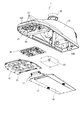
- FIG. 1 is a perspective view of a road lighting apparatus according to an embodiment of the present invention.
- FIG. 2 is a bottom view of the road lighting apparatus.
- FIG. 3 is an exploded perspective view of the road lighting fixture.
- FIG. 4 is a plan view of the LED light source substrate unit.
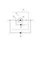
- FIG. 5 is a circuit diagram of the LED device and the first Zener diode.
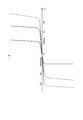
- FIG. 6 is a diagram schematically illustrating voltage-current characteristics of the first Zener diode and the LED device.
- FIG. 1 is a perspective view of a road lighting device 1 according to the present embodiment
- FIG. 2 is a bottom view of the road lighting device 1.
- FIG. 3 is an exploded perspective view of the road lighting device 1.
- the road lighting device 1 is a device that is attached to a column or the like standing on the road and illuminates the road surface of the road. As shown in FIGS. 1 to 3, the device main body 10, a bottom cover 11, and a lens are attached. A cover 12.
- the instrument body 10 is formed by die-casting (for example, aluminum die-casting) using a material having excellent thermal conductivity and corrosion resistance. As shown in FIG. Yes.
- a light source accommodating portion 15 described later is formed on the tip 10A side.
- the bottom surface cover 11 and the lens-equipped cover 12 are members that are attached to the bottom surface of the instrument body 10 and close the open portion of the bottom surface.
- the cover with lens 12 is attached at a position covering the light source housing 15 and covers the tip 10 ⁇ / b> A side of the instrument body 10.
- the bottom cover 11 covers the rear end 10B side of the instrument body 10 from the cover 12 with the lens.
- the bottom cover 11 is formed of a material having excellent thermal conductivity and corrosion resistance, like the instrument body 10. Further, the bottom cover 11 includes a hinge part 17 fixed to the instrument body 10 and a door plate 19 hinged to the hinge part 17, and the door plate 19 rotates downward with the hinge coupling portion as a fulcrum. open.
- the door plate 19 is non-rotatably screwed to the instrument body 10 on the side of the rear end 10B of the instrument body 10, and the screw is removed and released during maintenance work.
- the lens-equipped cover 12 is formed of a material that transmits light (for example, a resin material), and a large number of lenses 21 that control the distribution of transmitted light are integrally formed.
- a power supply box 23 is disposed inside the fixture body 10 at a position covered by the bottom cover 11, and an LED light source that is a light source of the road lighting fixture 1 is disposed in the light source housing 15.
- a substrate unit 30 is provided.
- the power supply box 23 houses a power supply circuit that supplies power to the LED light source board unit 30 and various electric circuit boards that control blinking and dimming of the LED device 32.
- an illuminance sensor socket 25 for detecting ambient brightness is provided on the upper surface of the fixture body 10, and the road lighting device 1 includes an illuminance sensor attached to the illuminance sensor socket 25. Turns on and off according to the detection result.
- the light source accommodating portion 15 includes a frame body 26 that divides a substantially rectangular region in bottom view inside the instrument main body 10, and a pedestal portion 27 that is provided in the region surrounded by the frame body 26. And.
- the pedestal portion 27 is a pedestal to which the LED light source substrate unit 30 is attached, and is formed integrally with the instrument body 10. The heat generated by the LED light source substrate unit 30 is transmitted from the pedestal portion 27 to the instrument body 10 and is radiated from, for example, the outer surface of the instrument body 10.
- FIG. 4 is a plan view of the LED light source substrate unit 30.
- the LED light source board unit 30 includes a circuit board 34, and a plurality of LED devices 32, which are examples of semiconductor light emitting elements, and a plurality of first Zener diodes 36 are mounted on the circuit board 34. Further, the circuit board 34 is provided with power feeding portions 39 and 39 to which the positive and negative electrodes of the power supply line are connected.
- the circuit board 34 is a metal board such as aluminum having high thermal conductivity. By directly attaching the circuit board 34 to the pedestal portion 27 of the instrument body 10, the heat generated by the LED device 32 is efficiently transmitted to the pedestal portion 27, and high heat dissipation performance is obtained.
- the LED mounting surface 34A of the circuit board 34 is entirely covered with a thin insulating layer.
- FIG. 5 is a circuit diagram of the LED device 32 and the first Zener diode 36.
- the LED device 32 includes an LED element 40 as an example of a light emitting element and a second Zener diode 41, and these are one electronic component packaged.
- the second Zener diode 41 is a protective element that protects the LED element 40 from static electricity, and is electrically connected in antiparallel to the LED element 40 inside the LED device 32.
- the second Zener diode 41 for electrostatic protection has a fast response speed and a small capacity. Note that any element can be used instead of the second Zener diode 41 as long as the element protects the LED element 40 from static electricity.
- an element that can short-circuit a reverse voltage that can be applied to the LED element 40 or can short-circuit a forward voltage that is higher than a predetermined voltage higher than the operating voltage of the LED element 40 is used as the protective element.
- an element include, in addition to a Zener diode, a diode connection of a transistor, an element in which the gate and source or drain of a MOSFET are short-circuited, or a composite element or IC thereof.
- the first Zener diode 36 is a protective element that protects the LED device 32 from a high-voltage test signal applied in the withstand voltage test and the withstand voltage test. They are electrically connected in reverse parallel.
- FIG. 6 is a diagram schematically illustrating voltage-current characteristics of the first Zener diode 36 and the LED device 32.
- the horizontal axis indicates the voltage V
- the vertical axis indicates the current I.
- the first Zener diode 36 has a characteristic that when the reverse voltage is applied to the LED device 32, the impedance becomes low impedance with the rising voltage Vthdiode as a boundary, and the current I flows rapidly.
- the rising voltage Vthdiode is a voltage having a smaller absolute value of the breakdown voltage Va of the LED element 40 and the breakdown voltage Vb of the second Zener diode 41 in the reverse voltage of the LED device 32 (illustrated example). Is set to a value lower than the breakdown voltage Va).
- the breakdown voltage is a voltage that causes an excessive current to flow and causes permanent damage or destruction of the element, and is a voltage that exceeds at least a rated voltage set so as not to cause damage or destruction.
- the first Zener diode 36 has a breakdown voltage Vc in the forward voltage of the LED device 32.
- the breakdown voltage Vc is set to be higher than the rising voltage Vthled emitted by the LED element 40 and lower than the breakdown voltage Vb ′ in the forward voltage of the second Zener diode 41.
- the first Zener diode 36 As the first Zener diode 36, a diode having a capacity high enough to prevent its own destruction by the test signal is selected, and the reliability of protection of the LED element 40 and the second Zener diode 41 is enhanced. In addition, the first Zener diode 36 has such a low reverse leakage current that a predetermined withstand voltage is obtained with respect to voltage application of a reverse voltage and a predetermined strength with respect to the withstand voltage. A diode having a high ESD (Electrostatic Discharge) breakdown voltage level is used. In addition, the first Zener diode 36 has a response frequency equal to or higher than the maximum frequency of the test signal, and protects the LED device 32 in the entire frequency band of the test signal.
- ESD Electrostatic Discharge
- this LED light source board unit 30 is provided with the metal circuit board 34, and the heat dissipation is improved.
- a high-voltage AC voltage is applied as a test signal between the power line of the road lighting fixture 1 and the fixture body 10.
- the LED light source substrate unit 30 is connected between the power supply unit 39 (FIG. 4) of the LED light source substrate unit 30 and the pedestal portion 27 that is a part of the instrument main body 10 to which the LED light source substrate unit 30 is attached.
- Voltage hereinafter referred to as “unit appliance voltage” occurs.
- the relationship between the voltage of the test signal and the voltage between unit instruments depends on the structure of the instrument body 10 and the circuit configuration of a power line (including an electric circuit such as a power circuit) and is difficult to consider quantitatively.
- the circuit board 34 is more electrically connected to the LED device 32 than the resin board when the circuit board 34 is a metal board. Load increases.
- the thickness of a general circuit board 34 used for an outdoor lighting fixture such as the road lighting fixture 1 is about 0.5 (mm) to 3 (mm).
- the circuit board 34 is a resin board
- the voltage between the unit appliances is a power supply portion 39 provided on the LED mounting surface 34A (FIG. 4) side of the circuit board 34 and wiring on the electrically connected LED mounting surface 34A.
- the opposite surface of the circuit board 34 that is in contact with the pedestal 27 of the instrument body 10, and the distance between them is substantially equal to the thickness of the circuit board 34.
- the circuit board 34 is a metal board such as an aluminum board
- the pedestal portion 27 of the instrument body 10 and the circuit board 34 are electrically connected, so that the voltage between the unit instruments is on the LED mounting surface 34A side of the circuit board 34.
- the thickness of the insulating layer is usually about 0.035 (mm) to 0.12 (mm).
- the circuit board 34 is configured by a metal board to which a larger voltage is applied to the LED device 32 by applying a test signal than in the case of a resin board. Even so, the LED device 32 can be sufficiently protected, and high heat dissipation performance is obtained.
- the LED device 32 is mounted on the circuit board 34 between the positive and negative power feeding portions 39 electrically connected in series. These LED devices 32 are annularly arranged in the plane of the circuit board 34, and each of the first Zener diodes 36 is arranged inside a range S surrounded by these LED devices 32. Since the first Zener diode 36 is disposed inside the range S surrounded by the LED devices 32, the circuit board 34 can be prevented from being enlarged.
- Each of the first Zener diodes 36 is disposed on a substantially central side of the circuit board 34, and the LED device 32 is disposed outside the first Zener diodes 36.
- the LED mounting surface 34A of the circuit board 34 is not electrically connected to the power feeding portions 39 and 39 in the region between the LED device 32 and the first Zener diode 36, and the wiring pattern and A planar pattern portion 42 (in the drawing, a hatched portion) formed of the same material is formed.
- each heat generation of the LED device 32 is guided to the surface pattern portion 42 to the outside of the center portion of the circuit board 34 and radiated, so that heat transfer from the LED device 32 to the first Zener diode 36 is performed.
- the first Zener diode 36 is protected from heat generation of the LED device 32.
- the circuit board 34 is provided with screw fixing holes 44 for screwing to the instrument body 10.
- screw fixing holes 44 for screwing to the instrument body 10.
- the circuit board 34 of the present embodiment is provided with the first Zener diode 36 that is connected in parallel to the LED device 32 and protects the LED device 32 from a high-voltage test signal. The destruction and damage of the LED device 32 due to the test signal applied in the test and withstand voltage test are prevented.
- the first Zener diode 36 is connected in parallel in the opposite direction to the polarity of the light emitting element, and the rising voltage Vthdiode is determined by the breakdown voltage Va of the LED element 40 and the breakdown voltage Vb of the second Zener diode 41.
- the absolute value of is lower than the smaller voltage.
- the first Zener diode 36 has the breakdown voltage Vc at the forward voltage higher than the rising voltage Vthled at which the LED element 40 emits light, and the breakdown voltage Vb ′ at the forward voltage of the second Zener diode 41. Is lower than.
- the LED 40 and the second Zener diode 41 can be protected from excessive forward voltage by causing a current to flow through the 40 and emitting light. Since not only the LED element 40 but also the second Zener diode 41 can be protected, resistance to overcurrent due to static electricity or the like can be maintained after the withstand voltage test.
- the circuit board 34 is a metal board, the LED device 32 is sufficiently protected by the first Zener diode 36 and high heat dissipation performance can be obtained.
- the circuit board 34 is configured by a metal substrate, but the circuit board 34 may be configured by a flexible substrate.
- the circuit board 34 formed of a flexible substrate may be directly attached to the pedestal portion 27 of the instrument main body 10 or may be attached with an insulating layer such as an insulating film interposed between the pedestal portion 27 and the pedestal portion 27.
- the thickness from the contact surface with the pedestal 27 to the power feeding portions 39, 39 of the circuit board 34 is thinner than that of the resin board.
- a stray capacitance (parasitic capacitance) larger than that of the resin substrate is generated, which causes a large charge transfer.
- the circuit board 34 is a flexible board
- a larger voltage is applied to the LED device 32 that changes its polarity in accordance with the application of the test signal that is an AC voltage, as compared with the resin board.
- the LED device 32 can be sufficiently protected from such a large voltage.
- any light emitting element such as an organic EL is used instead of the LED element 40.
- the circuit board 34 is connected in parallel to the LED device 32 and is similar to the first Zener diode 36 together with the first Zener diode 36 that protects the LED device 32 from a high-voltage test signal.
- one or more other elements such as a capacitor, a varistor, and a resistor that protect the LED device 32 from a high-voltage test signal may be provided.
- the lighting device of the present invention is not limited to the road lighting fixture 1 described above. That is, an illumination device that includes a light-emitting element and a semiconductor light-emitting element having a protective element that electrically protects the light-emitting element, and a circuit board provided with the semiconductor light-emitting element, and that illuminates by light emission of the light-emitting element If present, the present invention can be applied to any lighting device such as a lighting device used outdoors or indoors, or a lamp device such as an LED lamp.
Landscapes
- Circuit Arrangement For Electric Light Sources In General (AREA)
- Non-Portable Lighting Devices Or Systems Thereof (AREA)
Abstract
照明装置の絶縁耐圧試験ならびに耐電圧試験において印加される試験信号による半導体発光素子の破壊や損傷を防止する。 LED素子40、及び当該LED素子40を電気的に保護する第2ツェナーダイオード41を有したLEDデバイス32と、当該LEDデバイス32が設けられた回路基板34と、を備えた道路照明器具1において、前記回路基板34には、前記LEDデバイス32に並列接続され、高電圧の試験信号から前記LEDデバイス32を保護する第1ツェナーダイオード36が設けられている構成とした。
Description
本発明は、照明装置に関する。
従来、発光素子と、保護素子とが1つのパッケージ内に設けられた半導体発光素子が知られている(例えば、特許文献1、及び特許文献2参照)。保護素子は、静電気などによる過電流から発光素子を保護するための素子である。かかる半導体発光素子が照明装置の光源に用いられることで、静電気に対する耐性を有した照明装置の光源が実現される。
日本国内で販売される照明器具は全数、日本国内法令である電気用品安全法の規定により、絶縁耐圧試験ならびに耐電圧試験が実施されなければならない。
しかしながら、絶縁耐圧試験ならびに耐電圧試験における高電圧の試験信号の印加により、半導体発光素子に過大な電気信号が入力され、半導体発光素子が損傷あるいは破壊されることがある。
しかしながら、絶縁耐圧試験ならびに耐電圧試験における高電圧の試験信号の印加により、半導体発光素子に過大な電気信号が入力され、半導体発光素子が損傷あるいは破壊されることがある。
本発明は、照明器具の絶縁耐圧試験ならびに耐電圧試験において印加される試験信号による半導体発光素子の破壊や損傷を防止できる照明装置を提供することを目的とする。
本発明は、発光素子、及び当該発光素子を電気的に保護する保護素子を有した半導体発光素子と、当該半導体発光素子が設けられた回路基板と、を備えた照明装置において、前記回路基板には、前記半導体発光素子に並列接続され、高電圧の試験信号から前記半導体発光素子を保護するツェナーダイオードが設けられていることを特徴とする。
本発明は、上記照明装置において、前記ツェナーダイオードは、前記発光素子の極性と逆向きに並列接続されていることを特徴とする。
本発明は、上記照明装置において、前記ツェナーダイオードは、立ち上がり電圧が、前記発光素子の破壊電圧、及び前記保護素子の破壊電圧の絶対値が小さい方の電圧よりも低いことを特徴とする。
本発明は、上記照明装置において、前記ツェナーダイオードは、降伏電圧が、前記発光素子が発光する電圧よりも高く、かつ前記保護素子の順方向電圧における破壊電圧よりも低いことを特徴とする。
本発明は、上記照明装置において、前記回路基板は、金属基板、或いはフレキシブル基板であることを特徴とする。
本発明では、回路基板には、半導体発光素子に並列接続され、高電圧の試験信号から半導体発光素子を保護するツェナーダイオードが設けられているので、試験信号による半導体発光素子の破壊や損傷が防止される。
以下、図面を参照して本発明の実施形態について説明する。
本実施形態では、照明装置の一例として道路照明器具を例示する。
図1は本実施形態に係る道路照明器具1の斜視図であり、図2は道路照明器具1の底面図である。図3は道路照明器具1の分解斜視図である。
道路照明器具1は、道路に立設された支柱などに取り付けられ、道路の路面を照明する装置であり、図1~図3に示すように、器具本体10と、底面カバー11と、レンズ付カバー12と、を備える。
本実施形態では、照明装置の一例として道路照明器具を例示する。
図1は本実施形態に係る道路照明器具1の斜視図であり、図2は道路照明器具1の底面図である。図3は道路照明器具1の分解斜視図である。
道路照明器具1は、道路に立設された支柱などに取り付けられ、道路の路面を照明する装置であり、図1~図3に示すように、器具本体10と、底面カバー11と、レンズ付カバー12と、を備える。
器具本体10は、熱伝導性、及び耐食性に優れた材料を用いたダイキャスト成型(例えばアルミダイキャスト)によって形成され、図3に示すように、底面の略全面が開放した形状に形成されている。器具本体10の中には、先端10Aの側に、後述する光源収容部15が形成されている。
底面カバー11、及びレンズ付カバー12は、器具本体10の底面に取り付けられ、この底面の開放部を閉塞する部材である。レンズ付カバー12は光源収容部15を覆う位置に取り付けられ、器具本体10の先端10Aの側を覆っている。また底面カバー11は、レンズ付カバー12から器具本体10の後端10Bの側を覆っている。
底面カバー11、及びレンズ付カバー12は、器具本体10の底面に取り付けられ、この底面の開放部を閉塞する部材である。レンズ付カバー12は光源収容部15を覆う位置に取り付けられ、器具本体10の先端10Aの側を覆っている。また底面カバー11は、レンズ付カバー12から器具本体10の後端10Bの側を覆っている。
底面カバー11は、器具本体10と同様に、熱伝導性、及び耐食性に優れた材料によって形成されている。また底面カバー11は、器具本体10に固定されるヒンジ部品17と、このヒンジ部品17にヒンジ結合された扉板19とを備え、扉板19がヒンジ結合部分を支点に下方に回動して開く。扉板19は、器具本体10の後端10Bの側で器具本体10に回動不能にネジ止めされており、メンテナンス作業時にはネジが取り外されて開放される。
レンズ付カバー12は、光を透過する材料(例えば樹脂材)で形成され、透過光の配光を制御する多数のレンズ21が一体に形成されている。
器具本体10の内部には、図3に示すように、底面カバー11で覆われる位置に電源ボックス23が配置されており、また光源収容部15には、道路照明器具1の光源であるLED光源基板ユニット30が設けられている。
電源ボックス23には、LED光源基板ユニット30に電力を供給する電源回路や、LEDデバイス32の点滅、調光を制御する各種の電気回路基板が収められている。この道路照明器具1は、周囲の明るさを検出する照度センサ用のソケット25が器具本体10の上面に設けられており、道路照明器具1は、この照度センサ用のソケット25に取り付けた照度センサの検出結果に応じて点灯、消灯を行う。
電源ボックス23には、LED光源基板ユニット30に電力を供給する電源回路や、LEDデバイス32の点滅、調光を制御する各種の電気回路基板が収められている。この道路照明器具1は、周囲の明るさを検出する照度センサ用のソケット25が器具本体10の上面に設けられており、道路照明器具1は、この照度センサ用のソケット25に取り付けた照度センサの検出結果に応じて点灯、消灯を行う。
光源収容部15は、図3に示すように、器具本体10の内部に底面視略矩形の領域を区画する枠体26と、この枠体26で囲まれた領域内に設けられた台座部27とを備えている。台座部27は、LED光源基板ユニット30が取り付けられる台座であり、器具本体10に一体に形成されている。LED光源基板ユニット30の発熱は、台座部27から器具本体10に伝わり、例えば器具本体10の外表面などから放熱される。
図4は、LED光源基板ユニット30の平面図である。
LED光源基板ユニット30は、回路基板34を備え、この回路基板34には、半導体発光素子の一例たる複数のLEDデバイス32と、複数の第1ツェナーダイオード36とが実装されている。また、回路基板34には、電源ラインの正極、及び負極が接続される給電部39、39が設けられている。
回路基板34は、高熱伝導性を有する例えばアルミニウム等の金属基板である。この回路基板34が、器具本体10の台座部27に直接取り付けられることで、LEDデバイス32の発熱が台座部27に効率良く伝わり、高い放熱性能が得られる。
回路基板34のLED実装面34Aは、その表面の全体が薄い厚みの絶縁層で覆われている。
LED光源基板ユニット30は、回路基板34を備え、この回路基板34には、半導体発光素子の一例たる複数のLEDデバイス32と、複数の第1ツェナーダイオード36とが実装されている。また、回路基板34には、電源ラインの正極、及び負極が接続される給電部39、39が設けられている。
回路基板34は、高熱伝導性を有する例えばアルミニウム等の金属基板である。この回路基板34が、器具本体10の台座部27に直接取り付けられることで、LEDデバイス32の発熱が台座部27に効率良く伝わり、高い放熱性能が得られる。
回路基板34のLED実装面34Aは、その表面の全体が薄い厚みの絶縁層で覆われている。
図5は、LEDデバイス32、及び第1ツェナーダイオード36の回路図である。
同図に示すように、LEDデバイス32は、発光素子の一例たるLED素子40と、第2ツェナーダイオード41と、を有し、これらがパッケージ化された1つの電子部品である。第2ツェナーダイオード41は、静電気からLED素子40を保護する保護素子であり、LEDデバイス32の内部でLED素子40に体して逆並列に電気的に接続されている。一般に静電気保護用の第2ツェナーダイオード41は、応答速度が速く容量が小さい。
なお、静電気からLED素子40を保護する素子であれば、第2ツェナーダイオード41の代わりに、任意の素子を用いることができる。すなわち、保護素子には、LED素子40に印加される得る逆方向電圧を短絡したり、LED素子40の動作電圧より高い所定の電圧以上の順方向電圧をショートさせ得る素子が用いられる。このような素子には、例えばツェナーダイオードの他に、トランジスタのダイオード接続、MOSFETのゲートと、ソースまたはドレインとを短絡した素子、または、これらの複合素子、ICなどが挙げられる。
同図に示すように、LEDデバイス32は、発光素子の一例たるLED素子40と、第2ツェナーダイオード41と、を有し、これらがパッケージ化された1つの電子部品である。第2ツェナーダイオード41は、静電気からLED素子40を保護する保護素子であり、LEDデバイス32の内部でLED素子40に体して逆並列に電気的に接続されている。一般に静電気保護用の第2ツェナーダイオード41は、応答速度が速く容量が小さい。
なお、静電気からLED素子40を保護する素子であれば、第2ツェナーダイオード41の代わりに、任意の素子を用いることができる。すなわち、保護素子には、LED素子40に印加される得る逆方向電圧を短絡したり、LED素子40の動作電圧より高い所定の電圧以上の順方向電圧をショートさせ得る素子が用いられる。このような素子には、例えばツェナーダイオードの他に、トランジスタのダイオード接続、MOSFETのゲートと、ソースまたはドレインとを短絡した素子、または、これらの複合素子、ICなどが挙げられる。
第1ツェナーダイオード36は、絶縁耐圧試験ならびに耐電圧試験において印加される高電圧の試験信号からLEDデバイス32を保護する保護素子であり、回路基板34において、LEDデバイス32の極性と逆向き、すなわち逆並列に電気的に接続されている。
図6は、第1ツェナーダイオード36、及びLEDデバイス32の電圧電流特性を模式的に示す図である。同図において、横軸が電圧Vを示し、縦軸が電流Iを示す。
第1ツェナーダイオード36は、LEDデバイス32に逆方向電圧を印加していくと立ち上がり電圧Vthdiodeを境にして低インピーダンスとなり電流Iが急激に流れる特性を有する。
立ち上がり電圧Vthdiodeは、図6に示すように、LEDデバイス32の逆方向電圧において、LED素子40の破壊電圧Vaと第2ツェナーダイオード41の破壊電圧Vbとの絶対値が小さい方の電圧(図示例では、破壊電圧Va)よりも低い値に設定されている。なお、破壊電圧とは、過度な電流が流れて素子の永久的な損傷や破壊を生じさせる電圧であり、少なくとも損傷や破壊を生じさせないように設定された定格電圧を超えた電圧である。
第1ツェナーダイオード36は、LEDデバイス32に逆方向電圧を印加していくと立ち上がり電圧Vthdiodeを境にして低インピーダンスとなり電流Iが急激に流れる特性を有する。
立ち上がり電圧Vthdiodeは、図6に示すように、LEDデバイス32の逆方向電圧において、LED素子40の破壊電圧Vaと第2ツェナーダイオード41の破壊電圧Vbとの絶対値が小さい方の電圧(図示例では、破壊電圧Va)よりも低い値に設定されている。なお、破壊電圧とは、過度な電流が流れて素子の永久的な損傷や破壊を生じさせる電圧であり、少なくとも損傷や破壊を生じさせないように設定された定格電圧を超えた電圧である。
これにより、絶縁耐圧試験ならびに耐電圧試験において高電圧の試験信号が道路照明器具1に印加され、LED光源基板ユニット30の回路基板34に逆方向電圧が印可された場合でも、LED素子40、及び第2ツェナーダイオード41に破壊電圧Va、Vbが印加される前に第1ツェナーダイオード36に電流が流れる。したがって、LEDデバイス32内部への電気的負荷が低減され、これらLED素子40、及び第2ツェナーダイオード41の破壊や損傷が防止される。
さらに第1ツェナーダイオード36は、LEDデバイス32の順方向電圧において降伏電圧Vcを有する。降伏電圧Vcは、LED素子40が発光する立ち上がり電圧Vthledよりも高く、かつ、第2ツェナーダイオード41の順方向電圧における破壊電圧Vb’よりも低く設定されている。
これにより、道路照明器具1の通常使用時などにおいて、正常な電力が道路照明器具1に供給され、LED光源基板ユニット30の回路基板34に順方向電圧の定格の電圧が印加されたときには、第1ツェナーダイオード36に阻害されることなくLED素子40に電流が流れて発光し、かつ、第1ツェナーダイオード36が過剰な順方向電圧からLED素子40および第2ツェナーダイオード41を保護することができる。
これにより、道路照明器具1の通常使用時などにおいて、正常な電力が道路照明器具1に供給され、LED光源基板ユニット30の回路基板34に順方向電圧の定格の電圧が印加されたときには、第1ツェナーダイオード36に阻害されることなくLED素子40に電流が流れて発光し、かつ、第1ツェナーダイオード36が過剰な順方向電圧からLED素子40および第2ツェナーダイオード41を保護することができる。
この第1ツェナーダイオード36には、試験信号による自身の破壊が防止できる程度に容量が高いダイオードが選定されており、LED素子40および第2ツェナーダイオード41の保護の信頼性が高められている。
また、この第1ツェナーダイオード36には、逆方向電圧の電圧印加に対して所定の耐圧が得られるほどに逆方向漏れ電流が低く、かつ、耐圧に対して所定の強度が得られるほどに、ESD(Electrostatic Discharge)耐圧レベルが高いダイオードが用いられている。
これに加え、この第1ツェナーダイオード36は、試験信号の最大周波数以上の応答周波数を有しており、試験信号の全周波数帯域でLEDデバイス32を保護している。
また、この第1ツェナーダイオード36には、逆方向電圧の電圧印加に対して所定の耐圧が得られるほどに逆方向漏れ電流が低く、かつ、耐圧に対して所定の強度が得られるほどに、ESD(Electrostatic Discharge)耐圧レベルが高いダイオードが用いられている。
これに加え、この第1ツェナーダイオード36は、試験信号の最大周波数以上の応答周波数を有しており、試験信号の全周波数帯域でLEDデバイス32を保護している。
ところで、このLED光源基板ユニット30は、金属製の回路基板34を備えることで放熱性が高められている。
絶縁耐圧試験ならびに耐電圧試験においては、道路照明器具1の電源ラインと器具本体10の間に高電圧の交流電圧が試験信号として印加される。試験信号の印加により、LED光源基板ユニット30には、LED光源基板ユニット30の給電部39(図4)と、当該LED光源基板ユニット30が取り付けられる器具本体10の部位である台座部27の間に電圧(以下、「ユニット器具間電圧」という)が生じる。試験信号の電圧とユニット器具間電圧との関係は、器具本体10の構造や電源ライン(電源回路などの電気回路を含む)の回路構成などに依存し、定量的に考えることは難しい。
絶縁耐圧試験ならびに耐電圧試験においては、道路照明器具1の電源ラインと器具本体10の間に高電圧の交流電圧が試験信号として印加される。試験信号の印加により、LED光源基板ユニット30には、LED光源基板ユニット30の給電部39(図4)と、当該LED光源基板ユニット30が取り付けられる器具本体10の部位である台座部27の間に電圧(以下、「ユニット器具間電圧」という)が生じる。試験信号の電圧とユニット器具間電圧との関係は、器具本体10の構造や電源ライン(電源回路などの電気回路を含む)の回路構成などに依存し、定量的に考えることは難しい。
しかしながら、ユニット器具間電圧が同じであり、なおかつ、回路基板34の配線パターンが同じである場合、回路基板34が金属素材の基板である方が樹脂素材の基板よりもLEDデバイス32にかかる電気的な負荷が大きくなる。
詳述すると、道路照明器具1などの屋外照明器具に用いられる一般的な回路基板34の厚さは0.5(mm)~3(mm)程度である。
回路基板34が樹脂基板とした場合、ユニット器具間電圧は回路基板34のLED実装面34A(図4)の側に設けられた給電部39および電気的に接続されたLED実装面34A上の配線と、器具本体10の台座部27と接している回路基板34の反対側の面との間に印加され、その間隔はほぼ回路基板34の厚さに等しい。
一方、回路基板34がアルミ基板などの金属基板の場合、器具本体10の台座部27と、回路基板34とは導通しているため、ユニット器具間電圧は回路基板34のLED実装面34Aの側に設けられた給電部39および電気的に接続されたLED実装面34A上の配線と、回路基板34のLED実装面34Aの側の表面に施された絶縁層を挟んで回路基板34の金属部との間に印加される。絶縁層の厚みは、通常、0.035(mm)~0.12(mm)程度である。
このため、回路基板34が金属基板である場合、樹脂基板より大きな浮遊容量(寄生容量)が生じ、大きな電荷の移動を招くので、交流電圧である試験信号の印加にしたがって極性が変わる大きな電圧がLEDデバイス32に加わることになる。
回路基板34が樹脂基板とした場合、ユニット器具間電圧は回路基板34のLED実装面34A(図4)の側に設けられた給電部39および電気的に接続されたLED実装面34A上の配線と、器具本体10の台座部27と接している回路基板34の反対側の面との間に印加され、その間隔はほぼ回路基板34の厚さに等しい。
一方、回路基板34がアルミ基板などの金属基板の場合、器具本体10の台座部27と、回路基板34とは導通しているため、ユニット器具間電圧は回路基板34のLED実装面34Aの側に設けられた給電部39および電気的に接続されたLED実装面34A上の配線と、回路基板34のLED実装面34Aの側の表面に施された絶縁層を挟んで回路基板34の金属部との間に印加される。絶縁層の厚みは、通常、0.035(mm)~0.12(mm)程度である。
このため、回路基板34が金属基板である場合、樹脂基板より大きな浮遊容量(寄生容量)が生じ、大きな電荷の移動を招くので、交流電圧である試験信号の印加にしたがって極性が変わる大きな電圧がLEDデバイス32に加わることになる。
本実施形態では、上記第1ツェナーダイオード36が回路基板34に設けられているので、樹脂基板の場合よりも試験信号の印加によって大きな電圧がLEDデバイス32に加わる金属基板で回路基板34を構成していても、LEDデバイス32を十分に保護することができ、なおかつ、高い放熱性能が得られている。
次いで回路基板34のLED実装面34Aのレイアウト構造について説明する。
前掲図4に示すように、回路基板34には、正極、及び負極の給電部39の間に、LEDデバイス32が電気的に直列に接続されて実装されている。これらのLEDデバイス32は、回路基板34の面内に環状に配置され、これらのLEDデバイス32に囲まれた範囲Sの内側に、第1ツェナーダイオード36のそれぞれが配置されている。
LEDデバイス32に囲まれた範囲Sの内側に第1ツェナーダイオード36が配置されるので、回路基板34の大型化が防がれる。
前掲図4に示すように、回路基板34には、正極、及び負極の給電部39の間に、LEDデバイス32が電気的に直列に接続されて実装されている。これらのLEDデバイス32は、回路基板34の面内に環状に配置され、これらのLEDデバイス32に囲まれた範囲Sの内側に、第1ツェナーダイオード36のそれぞれが配置されている。
LEDデバイス32に囲まれた範囲Sの内側に第1ツェナーダイオード36が配置されるので、回路基板34の大型化が防がれる。
第1ツェナーダイオード36の各々は回路基板34の略中央部の側に配置されており、これら第1ツェナーダイオード36の外側にLEDデバイス32が配置されている。
また、回路基板34のLED実装面34Aには、LEDデバイス32と、第1ツェナーダイオード36との間の領域に、給電部39、39とは電気的に接続されておらず、かつ配線パターンと同一素材で形成された面状パターン部42(図示中、斜線箇所)が形成されている。
これにより、LEDデバイス32の各々の発熱は、回路基板34の中央部よりも外側へ面状パターン部42に誘導されて放熱されるので、LEDデバイス32から第1ツェナーダイオード36への熱伝達が抑えられ、第1ツェナーダイオード36がLEDデバイス32の発熱から保護される。
また、回路基板34のLED実装面34Aには、LEDデバイス32と、第1ツェナーダイオード36との間の領域に、給電部39、39とは電気的に接続されておらず、かつ配線パターンと同一素材で形成された面状パターン部42(図示中、斜線箇所)が形成されている。
これにより、LEDデバイス32の各々の発熱は、回路基板34の中央部よりも外側へ面状パターン部42に誘導されて放熱されるので、LEDデバイス32から第1ツェナーダイオード36への熱伝達が抑えられ、第1ツェナーダイオード36がLEDデバイス32の発熱から保護される。
回路基板34には器具本体10にネジ止めするためのネジ止め固定用孔44が設けられている。このネジ止め固定用孔44に通されるネジを高熱伝導材とすることで、回路基板34の中央部から器具本体10への放熱性を高めることもできる。
以上説明したように、本実施形態の回路基板34には、LEDデバイス32に並列接続され、高電圧の試験信号からLEDデバイス32を保護する第1ツェナーダイオード36が設けられているので、絶縁耐圧試験ならびに耐電圧試験において印加される試験信号によるLEDデバイス32の破壊や損傷が防止される。
また本実施形態では、第1ツェナーダイオード36は、発光素子の極性と逆向きに並列接続されており、立ち上がり電圧Vthdiodeが、LED素子40の破壊電圧Va、及び第2ツェナーダイオード41の破壊電圧Vbの絶対値が小さい方の電圧よりも低くなっている。
これにより、高電圧の試験信号によりLED光源基板ユニット30の回路基板34に逆方向電圧が印可された場合でも、LED素子40、及び第2ツェナーダイオード41に破壊電圧Va、Vbが印加される前に第1ツェナーダイオード36に電流が流れる。したがって、LEDデバイス32内部への電気的負荷が低減され、これらLED素子40、及び第2ツェナーダイオード41の破壊や損傷が防止される。
これにより、高電圧の試験信号によりLED光源基板ユニット30の回路基板34に逆方向電圧が印可された場合でも、LED素子40、及び第2ツェナーダイオード41に破壊電圧Va、Vbが印加される前に第1ツェナーダイオード36に電流が流れる。したがって、LEDデバイス32内部への電気的負荷が低減され、これらLED素子40、及び第2ツェナーダイオード41の破壊や損傷が防止される。
また本実施形態では、第1ツェナーダイオード36は、順方向電圧における降伏電圧Vcが、LED素子40が発光する立ち上がり電圧Vthledよりも高く、かつ第2ツェナーダイオード41の順方向電圧における破壊電圧Vb’よりも低くなっている。
これにより、道路照明器具1の通常使用時などにおいて、LED光源基板ユニット30の回路基板34に順方向電圧の定格の電圧が印加されたときには、第1ツェナーダイオード36に阻害されることなくLED素子40に電流が流れて発光し、かつ、第1ツェナーダイオード36が過剰な順方向電圧からLED素子40および第2ツェナーダイオード41を保護することができる。LED素子40だけでなく第2ツェナーダイオード41も保護できるので、耐電圧試験後も静電気などによる過電流に対する耐性を維持できる。
これにより、道路照明器具1の通常使用時などにおいて、LED光源基板ユニット30の回路基板34に順方向電圧の定格の電圧が印加されたときには、第1ツェナーダイオード36に阻害されることなくLED素子40に電流が流れて発光し、かつ、第1ツェナーダイオード36が過剰な順方向電圧からLED素子40および第2ツェナーダイオード41を保護することができる。LED素子40だけでなく第2ツェナーダイオード41も保護できるので、耐電圧試験後も静電気などによる過電流に対する耐性を維持できる。
また本実施形態では、回路基板34が金属基板であるので、上記第1ツェナーダイオード36によりLEDデバイス32を十分に保護、なおかつ、高い放熱性能が得られる。
なお、上述した実施形態は、あくまでも本発明の一態様を例示したものであって、本発明の趣旨を逸脱しない範囲で任意に変形、及び応用が可能である。
上述した実施形態において、回路基板34を金属基板により構成した場合を例示したが、回路基板34をフレキシブル基板によって構成してもよい。フレキシブル基板から成る回路基板34は、器具本体10の台座部27に直接取り付けられてもよいし、台座部27との間に絶縁フィルムなどの絶縁層を挟んで取り付けられてもよい。いずれの取付態様においても、台座部27との接触面から回路基板34の給電部39、39までの厚みは樹脂基板に比較して薄い。
このように厚みが薄くなると、樹脂基板より大きな浮遊容量(寄生容量)が生じ、大きな電荷の移動を招く。したがって、回路基板34がフレキシブル基板であると、樹脂基板に比べ、交流電圧である試験信号の印加にしたがって極性が変わる大きな電圧がLEDデバイス32にかかる。
そして、回路基板34に、上記第1ツェナーダイオード36が設けられることで、このような大きな電圧からLEDデバイス32を十分に保護できるのである。
このように厚みが薄くなると、樹脂基板より大きな浮遊容量(寄生容量)が生じ、大きな電荷の移動を招く。したがって、回路基板34がフレキシブル基板であると、樹脂基板に比べ、交流電圧である試験信号の印加にしたがって極性が変わる大きな電圧がLEDデバイス32にかかる。
そして、回路基板34に、上記第1ツェナーダイオード36が設けられることで、このような大きな電圧からLEDデバイス32を十分に保護できるのである。
また上述した実施形態において、LED素子40に代えて、有機ELなどの任意の発光素子が用いられる。
また上述した実施形態において、回路基板34には、LEDデバイス32に並列接続され、高電圧の試験信号からLEDデバイス32を保護する第1ツェナーダイオード36と併せて、当該第1ツェナーダイオード36と同様に高電圧の試験信号からLEDデバイス32を保護するコンデンサやバリスタ、抵抗などの1又は複数の他の素子が設けられてもよい。
また本発明の照明装置は、上述した道路照明器具1に限らない。すなわち、発光素子、及び当該発光素子を電気的に保護する保護素子を有した半導体発光素子と、当該半導体発光素子が設けられた回路基板と、を備え、発光素子の発光によって照明する照明装置であれば、本発明は、屋外、或いは屋内で用いられる照明器具、或いはLEDランプなどのランプ装置といった任意の照明装置に適用できる。
1 道路照明器具(照明装置)
10 器具本体
15 光源収容部
27 台座部
30 LED光源基板ユニット
32 LEDデバイス(半導体発光素子)
34 回路基板
34A LED実装面
36 第1ツェナーダイオード(ツェナーダイオード)
39 給電部
40 LED素子(発光素子)
41 第2ツェナーダイオード(保護素子)
42 面状パターン部
44 孔
Va、Vb、Vb’ 破壊電圧
Vc 降伏電圧
Vthdiode ツェナーダイオードの立ち上がり電圧
Vthled LED素子の立ち上がり電圧
10 器具本体
15 光源収容部
27 台座部
30 LED光源基板ユニット
32 LEDデバイス(半導体発光素子)
34 回路基板
34A LED実装面
36 第1ツェナーダイオード(ツェナーダイオード)
39 給電部
40 LED素子(発光素子)
41 第2ツェナーダイオード(保護素子)
42 面状パターン部
44 孔
Va、Vb、Vb’ 破壊電圧
Vc 降伏電圧
Vthdiode ツェナーダイオードの立ち上がり電圧
Vthled LED素子の立ち上がり電圧
Claims (5)
- 発光素子、及び当該発光素子を電気的に保護する保護素子を有した半導体発光素子と、当該半導体発光素子が設けられた回路基板と、を備えた照明装置において、
前記回路基板には、
前記半導体発光素子に並列接続され、高電圧の試験信号から前記半導体発光素子を保護するツェナーダイオードが設けられている
ことを特徴とする照明装置。 - 前記ツェナーダイオードは、前記発光素子の極性と逆向きに並列接続されていることを特徴とする請求項1に記載の照明装置。
- 前記ツェナーダイオードは、
立ち上がり電圧が、前記発光素子の破壊電圧、及び前記保護素子の破壊電圧の絶対値が小さい方の電圧よりも低い
ことを特徴とする請求項1または2に記載の照明装置。 - 前記ツェナーダイオードは、
降伏電圧が、前記発光素子が発光する電圧よりも高く、かつ前記保護素子の順方向電圧における破壊電圧よりも低い
ことを特徴とする請求項1~3のいずれかに記載の照明装置。 - 前記回路基板は、金属基板、或いはフレキシブル基板である
ことを特徴とする請求項1~4のいずれかに記載の照明装置。
Priority Applications (1)
| Application Number | Priority Date | Filing Date | Title |
|---|---|---|---|
| PCT/JP2016/060310 WO2017168604A1 (ja) | 2016-03-30 | 2016-03-30 | 照明装置 |
Applications Claiming Priority (1)
| Application Number | Priority Date | Filing Date | Title |
|---|---|---|---|
| PCT/JP2016/060310 WO2017168604A1 (ja) | 2016-03-30 | 2016-03-30 | 照明装置 |
Publications (1)
| Publication Number | Publication Date |
|---|---|
| WO2017168604A1 true WO2017168604A1 (ja) | 2017-10-05 |
Family
ID=59963697
Family Applications (1)
| Application Number | Title | Priority Date | Filing Date |
|---|---|---|---|
| PCT/JP2016/060310 Ceased WO2017168604A1 (ja) | 2016-03-30 | 2016-03-30 | 照明装置 |
Country Status (1)
| Country | Link |
|---|---|
| WO (1) | WO2017168604A1 (ja) |
Citations (5)
| Publication number | Priority date | Publication date | Assignee | Title |
|---|---|---|---|---|
| JP2002335012A (ja) * | 1999-02-25 | 2002-11-22 | Nichia Chem Ind Ltd | 発光ダイオード及びそれを用いたドットマトリックスディスプレイ |
| JP2011139072A (ja) * | 2009-12-29 | 2011-07-14 | Tai-Her Yang | 電圧制限及び逆極性直列接続式led装置 |
| JP2014110301A (ja) * | 2012-11-30 | 2014-06-12 | Panasonic Corp | 発光装置および照明用光源 |
| JP2014241202A (ja) * | 2013-06-11 | 2014-12-25 | スタンレー電気株式会社 | 車両用灯具におけるled点灯装置 |
| JP2015056379A (ja) * | 2013-09-13 | 2015-03-23 | パナソニックIpマネジメント株式会社 | 照明用光源及び照明装置 |
-
2016
- 2016-03-30 WO PCT/JP2016/060310 patent/WO2017168604A1/ja not_active Ceased
Patent Citations (5)
| Publication number | Priority date | Publication date | Assignee | Title |
|---|---|---|---|---|
| JP2002335012A (ja) * | 1999-02-25 | 2002-11-22 | Nichia Chem Ind Ltd | 発光ダイオード及びそれを用いたドットマトリックスディスプレイ |
| JP2011139072A (ja) * | 2009-12-29 | 2011-07-14 | Tai-Her Yang | 電圧制限及び逆極性直列接続式led装置 |
| JP2014110301A (ja) * | 2012-11-30 | 2014-06-12 | Panasonic Corp | 発光装置および照明用光源 |
| JP2014241202A (ja) * | 2013-06-11 | 2014-12-25 | スタンレー電気株式会社 | 車両用灯具におけるled点灯装置 |
| JP2015056379A (ja) * | 2013-09-13 | 2015-03-23 | パナソニックIpマネジメント株式会社 | 照明用光源及び照明装置 |
Similar Documents
| Publication | Publication Date | Title |
|---|---|---|
| US9920909B2 (en) | Lighting driver and housing having internal electromagnetic shielding layer configured for direct connection to circuit ground | |
| US9609717B2 (en) | Light-emitting apparatus and lighting appliance provided with the same | |
| CN106851890A (zh) | 具有漏电流保护电路的镇流稳定器可兼容灯 | |
| US9188314B2 (en) | Light emitting diode device | |
| US20120313551A1 (en) | Lamp Device | |
| US9279577B2 (en) | LED lighting device and method for making the same | |
| US11674678B2 (en) | Apparatus with charge dissipation | |
| US20050173713A1 (en) | Multi-pin light-emitting diode device | |
| JP6766290B2 (ja) | サージ保護照明器具 | |
| JP5553977B2 (ja) | Led照明器具 | |
| WO2017168604A1 (ja) | 照明装置 | |
| JP6384689B2 (ja) | 照明装置 | |
| JP6620849B2 (ja) | 照明装置 | |
| JP2020024954A (ja) | 照明装置 | |
| JP2019114341A (ja) | 照明装置 | |
| JP6615295B2 (ja) | 電源装置及び照明装置 | |
| JP2006286702A (ja) | Led実装用基板 | |
| JP7121922B2 (ja) | 電源回路及び照明装置 | |
| JP2025086720A (ja) | 電源装置及び照明器具 | |
| JP2016162595A (ja) | 照明器具 | |
| WO2021079311A1 (en) | Led lighting device with overvoltage protection system | |
| JP2025023570A (ja) | 車両用照明装置、および車両用灯具 | |
| CN206234627U (zh) | 灯装置及照明装置 | |
| JP2019216127A (ja) | 照明装置 |
Legal Events
| Date | Code | Title | Description |
|---|---|---|---|
| NENP | Non-entry into the national phase |
Ref country code: DE |
|
| 121 | Ep: the epo has been informed by wipo that ep was designated in this application |
Ref document number: 16896824 Country of ref document: EP Kind code of ref document: A1 |
|
| 122 | Ep: pct application non-entry in european phase |
Ref document number: 16896824 Country of ref document: EP Kind code of ref document: A1 |
|
| NENP | Non-entry into the national phase |
Ref country code: JP |