WO2017169505A1 - Dispositif de prise de vue à semi-conducteurs, procédé de fabrication de dispositif de prise de vue à semi-conducteurs et appareil électronique - Google Patents
Dispositif de prise de vue à semi-conducteurs, procédé de fabrication de dispositif de prise de vue à semi-conducteurs et appareil électronique Download PDFInfo
- Publication number
- WO2017169505A1 WO2017169505A1 PCT/JP2017/008404 JP2017008404W WO2017169505A1 WO 2017169505 A1 WO2017169505 A1 WO 2017169505A1 JP 2017008404 W JP2017008404 W JP 2017008404W WO 2017169505 A1 WO2017169505 A1 WO 2017169505A1
- Authority
- WO
- WIPO (PCT)
- Prior art keywords
- conductor
- semiconductor chip
- solid
- imaging device
- state imaging
- Prior art date
- Legal status (The legal status is an assumption and is not a legal conclusion. Google has not performed a legal analysis and makes no representation as to the accuracy of the status listed.)
- Ceased
Links
Images


Classifications
-
- H—ELECTRICITY
- H10—SEMICONDUCTOR DEVICES; ELECTRIC SOLID-STATE DEVICES NOT OTHERWISE PROVIDED FOR
- H10F—INORGANIC SEMICONDUCTOR DEVICES SENSITIVE TO INFRARED RADIATION, LIGHT, ELECTROMAGNETIC RADIATION OF SHORTER WAVELENGTH OR CORPUSCULAR RADIATION
- H10F39/00—Integrated devices, or assemblies of multiple devices, comprising at least one element covered by group H10F30/00, e.g. radiation detectors comprising photodiode arrays
- H10F39/80—Constructional details of image sensors
- H10F39/802—Geometry or disposition of elements in pixels, e.g. address-lines or gate electrodes
-
- H—ELECTRICITY
- H10—SEMICONDUCTOR DEVICES; ELECTRIC SOLID-STATE DEVICES NOT OTHERWISE PROVIDED FOR
- H10F—INORGANIC SEMICONDUCTOR DEVICES SENSITIVE TO INFRARED RADIATION, LIGHT, ELECTROMAGNETIC RADIATION OF SHORTER WAVELENGTH OR CORPUSCULAR RADIATION
- H10F39/00—Integrated devices, or assemblies of multiple devices, comprising at least one element covered by group H10F30/00, e.g. radiation detectors comprising photodiode arrays
- H10F39/80—Constructional details of image sensors
- H10F39/809—Constructional details of image sensors of hybrid image sensors
-
- H—ELECTRICITY
- H04—ELECTRIC COMMUNICATION TECHNIQUE
- H04N—PICTORIAL COMMUNICATION, e.g. TELEVISION
- H04N25/00—Circuitry of solid-state image sensors [SSIS]; Control thereof
- H04N25/70—SSIS architectures; Circuits associated therewith
-
- H—ELECTRICITY
- H10—SEMICONDUCTOR DEVICES; ELECTRIC SOLID-STATE DEVICES NOT OTHERWISE PROVIDED FOR
- H10F—INORGANIC SEMICONDUCTOR DEVICES SENSITIVE TO INFRARED RADIATION, LIGHT, ELECTROMAGNETIC RADIATION OF SHORTER WAVELENGTH OR CORPUSCULAR RADIATION
- H10F39/00—Integrated devices, or assemblies of multiple devices, comprising at least one element covered by group H10F30/00, e.g. radiation detectors comprising photodiode arrays
- H10F39/011—Manufacture or treatment of image sensors covered by group H10F39/12
- H10F39/018—Manufacture or treatment of image sensors covered by group H10F39/12 of hybrid image sensors
-
- H—ELECTRICITY
- H10—SEMICONDUCTOR DEVICES; ELECTRIC SOLID-STATE DEVICES NOT OTHERWISE PROVIDED FOR
- H10F—INORGANIC SEMICONDUCTOR DEVICES SENSITIVE TO INFRARED RADIATION, LIGHT, ELECTROMAGNETIC RADIATION OF SHORTER WAVELENGTH OR CORPUSCULAR RADIATION
- H10F39/00—Integrated devices, or assemblies of multiple devices, comprising at least one element covered by group H10F30/00, e.g. radiation detectors comprising photodiode arrays
- H10F39/80—Constructional details of image sensors
- H10F39/811—Interconnections
-
- H—ELECTRICITY
- H10—SEMICONDUCTOR DEVICES; ELECTRIC SOLID-STATE DEVICES NOT OTHERWISE PROVIDED FOR
- H10F—INORGANIC SEMICONDUCTOR DEVICES SENSITIVE TO INFRARED RADIATION, LIGHT, ELECTROMAGNETIC RADIATION OF SHORTER WAVELENGTH OR CORPUSCULAR RADIATION
- H10F39/00—Integrated devices, or assemblies of multiple devices, comprising at least one element covered by group H10F30/00, e.g. radiation detectors comprising photodiode arrays
- H10F39/10—Integrated devices
- H10F39/12—Image sensors
- H10F39/199—Back-illuminated image sensors
-
- H—ELECTRICITY
- H10—SEMICONDUCTOR DEVICES; ELECTRIC SOLID-STATE DEVICES NOT OTHERWISE PROVIDED FOR
- H10F—INORGANIC SEMICONDUCTOR DEVICES SENSITIVE TO INFRARED RADIATION, LIGHT, ELECTROMAGNETIC RADIATION OF SHORTER WAVELENGTH OR CORPUSCULAR RADIATION
- H10F39/00—Integrated devices, or assemblies of multiple devices, comprising at least one element covered by group H10F30/00, e.g. radiation detectors comprising photodiode arrays
- H10F39/80—Constructional details of image sensors
- H10F39/805—Coatings
- H10F39/8057—Optical shielding
Definitions
- the present technology relates to a solid-state imaging device, a manufacturing method of the solid-state imaging device, and an electronic apparatus, and particularly relates to a technology of a solid-state imaging device configured by joining a plurality of semiconductor chips.
- mobile terminals such as mobile phones, PDAs (Personal Digital Assistants), notebook PCs (Personal Computers), and tablet PCs
- an imaging function are also spreading.
- the solid-state imaging device and the components constituting it have been reduced in size, weight, and thickness.
- the cost of solid-state imaging devices and parts constituting them is being reduced.
- a solid-state imaging device such as a CMOS (Complementary Metal Oxide Semiconductor) image sensor forms a photoelectric conversion unit, an amplifier circuit, and a multilayer wiring layer on a light receiving surface side of a silicon substrate, and a color filter and an on-layer are formed thereon. It is configured by forming a semiconductor chip microlens. Further, a cover glass is bonded to the light receiving surface side by a spacer such as an adhesive. A terminal is formed on the opposite side of the light receiving surface.
- CMOS Complementary Metal Oxide Semiconductor
- This signal processing device is connected to a signal processing circuit that performs predetermined processing on the output signal.
- a signal processing circuit that performs predetermined processing on the output signal.
- SiP System-in-Package
- Patent Document 1 describes a solid-state imaging device configured by bonding and bonding a first semiconductor substrate including a pixel region (pixel array) and a second semiconductor substrate including a logic circuit. Has been. According to such a configuration, a signal can be transmitted at high speed.
- a first semiconductor chip portion having a pixel array in a semi-finished product state is bonded to a second semiconductor chip portion having a logic circuit, and the first semiconductor chip portion is thinned. Thereafter, the pixel array and the logic circuit are connected.
- connection includes a connection conductor connected to the required wiring of the first semiconductor chip portion, a through connection conductor passing through the first semiconductor chip portion and connected to the required wiring of the second semiconductor chip portion, and both connections This is performed by forming a connection wiring composed of a connecting conductor that connects the conductors. After that, a finished product is formed into a semiconductor chip, which is configured as a back-illuminated solid-state imaging device.
- the copper (Cu) electrode is used for the light shielding layer.
- the light shielding layer As a result, light emission from the hot carriers from the transistors of the logic circuit is blocked by the light blocking layer, and incidence on the pixel array side is suppressed.
- the thickness of the entire semiconductor chip after bonding is also suppressed.
- the region that cannot be bonded is generated by increasing the ratio of the area ratio of the copper electrode, so that the bonding-wave speed at the time of Wafer To Wafer Bonding becomes uneven, and as a result, at the outer periphery of the wafer, It is considered that a portion where the joining speed becomes relatively slow occurs, and a region that cannot be joined, that is, a void is formed.
- the present technology has been made in view of such a situation, and provides a solid-state imaging device capable of suppressing the generation of voids by realizing wafer bonding of a conductive film having a high area ratio at a bonding surface of a plurality of semiconductor chips.
- the purpose is to do.
- a solid-state imaging device as an example of the present technology is bonded to a first semiconductor chip on which one or a plurality of first conductors and a pixel array are formed, and the first semiconductor chip.
- the body and the second conductor overlap and are electrically connected, and the area in contact with the bonding surface is different between the first conductor and the second conductor.
- a method for manufacturing a solid-state imaging device includes a step of forming one or more first conductors and a pixel array on a first semiconductor chip, and one or more second conductors. Forming the body and the logic circuit on the second semiconductor chip, and overlapping the first conductor formed on the first semiconductor chip and the second conductor formed on the second semiconductor chip. The first conductor and the second conductor have different areas in contact with the bonding surface between the first semiconductor chip and the second semiconductor chip.
- an electronic apparatus that is an example of the present technology includes a first semiconductor chip in which one or a plurality of first conductors and a pixel array are formed, and a first semiconductor chip that is bonded to the first semiconductor chip.
- the solid-state imaging device includes a body that overlaps and is electrically connected, and an area in contact with the joint surface is different between the first conductor and the second conductor.
- the present technology it is possible to provide a solid-state imaging device capable of suppressing the generation of voids by realizing wafer bonding of a conductive film having a high area ratio at bonding surfaces of a plurality of semiconductor chips.
- the effects of the present technology are not necessarily limited to the above effects, and may be any of the effects described in the present disclosure.
- FIG. 6 is a manufacturing process diagram (part 1) illustrating an example of a manufacturing method of the solid-state imaging device according to the first embodiment; It is a manufacturing process figure (the 2) which shows the example of a manufacturing method of the solid-state imaging device of a 1st embodiment.
- FIG. 10 is a manufacturing process diagram (part 5) illustrating an example of a manufacturing method of the solid-state imaging device according to the first embodiment; It is a manufacturing process figure (the 6) which shows the example of a manufacturing method of the solid-state imaging device of 1st Embodiment. It is a manufacturing process figure (the 7) which shows the example of a manufacturing method of the solid-state imaging device of a 1st embodiment.
- the manufacturing process figure (the 8) which shows the example of a manufacturing method of the solid-state imaging device of a 1st embodiment. It is a manufacturing process figure (the 9) which shows the example of a manufacturing method of the solid-state imaging device of a 1st embodiment. It is a schematic block diagram which shows the principal part of 2nd Embodiment of the solid-state imaging device which concerns on this technique. It is a schematic block diagram which shows the principal part of 3rd Embodiment of the solid-state imaging device which concerns on this technique. It is a schematic block diagram which shows the principal part of 4th Embodiment of the solid-state imaging device which concerns on this technique.
- FIG. 1 is a block diagram illustrating a configuration example of a solid-state imaging device according to the present technology.
- the solid-state imaging device 1 is configured as, for example, a CMOS (Complementary Metal Metal Oxide Semiconductor) image sensor.
- the solid-state imaging device 1 includes a pixel region (pixel array) 3 in which a plurality of pixels 2 are regularly arranged in a two-dimensional array on a semiconductor substrate (for example, Si substrate) (not shown), and a peripheral circuit unit.
- CMOS Complementary Metal Metal Oxide Semiconductor
- the pixel 2 has a photoelectric conversion unit (for example, a photodiode) and a plurality of pixel transistors (MOS transistors).
- the plurality of pixel transistors can be constituted by three transistors, for example, a transfer transistor, a reset transistor, and an amplification transistor.
- the plurality of pixel transistors can be configured by four transistors by adding selection transistors. Since the equivalent circuit of the unit pixel is the same as that of a well-known technique, detailed description thereof is omitted.
- the pixel 2 can be configured as one unit pixel or a shared pixel structure.
- This pixel sharing structure is a structure in which a plurality of photodiodes share a transistor other than the floating diffusion and the plurality of transfer transistors. That is, in the shared pixel, a photodiode and a transfer transistor that form a plurality of unit pixels are configured by sharing each other pixel transistor.
- the peripheral circuit section has a vertical drive circuit 4, a column signal processing circuit 5, a horizontal drive circuit 6, an output circuit 7, and a control circuit 8.
- the vertical drive circuit 4 is constituted by a shift register, for example.
- the vertical drive circuit 4 selects a pixel drive wiring, supplies a pulse for driving the pixel to the selected pixel drive wiring, and drives the pixels in units of rows. That is, the vertical drive circuit 4 selectively scans each pixel 2 of the pixel array 3 in the vertical direction sequentially in units of rows.
- the vertical drive circuit 4 supplies the column signal processing circuit 5 with a pixel signal based on the signal charge generated according to the amount of received light in the photoelectric conversion unit of each pixel 2 through the vertical signal line 9.
- the column signal processing circuit 5 is arranged for each column of the pixels 2, for example.
- the column signal processing circuit 5 performs signal processing such as noise removal for each pixel column on the signal output from the pixels 2 for one row.
- the column signal processing circuit 5 performs signal processing such as CDS (Correlated Double Sampling) for removing fixed pattern noise unique to the pixel 2, signal amplification, A / D (Analog / Digital) conversion, and the like.
- CDS Correlated Double Sampling
- a / D Analog / Digital
- the horizontal drive circuit 6 is constituted by a shift register, for example.
- the horizontal drive circuit 6 sequentially selects the column signal processing circuits 5 by sequentially outputting horizontal scanning pulses, and outputs the pixel signals from the column signal processing circuits 5 to the horizontal signal line 10.
- the output circuit 7 performs signal processing on the signals sequentially supplied from each of the column signal processing circuits 5 through the horizontal signal line 10 and outputs the signals.
- the output circuit 7 may perform only buffering, or may perform black level adjustment, column variation correction, various digital signal processing, and the like.
- the control circuit 8 receives an input clock and data for instructing an operation mode, and outputs data such as internal information of the solid-state imaging device 1. In addition, the control circuit 8 receives a clock signal and a control signal that serve as a reference for operations of the vertical drive circuit 4, the column signal processing circuit 5, the horizontal drive circuit 6 and the like based on the vertical synchronization signal, the horizontal synchronization signal, and the master clock. Generate. The control circuit 8 inputs these signals to the vertical drive circuit 4, the column signal processing circuit 5, the horizontal drive circuit 6, and the like.
- the input / output terminal 12 exchanges signals with the outside.
- Example of laminated structure of solid-state imaging device> 2A to 2C are schematic views illustrating a stacked structure example of the solid-state imaging device according to the present technology. A stacked structure example of a solid-state imaging device to which the present technology is applied will be described with reference to FIGS. 2A to 2C.
- the solid-state imaging device 1a shown in FIG. 2A includes a first semiconductor substrate 21 and a second semiconductor substrate 22.
- a pixel array 23 and a control circuit 24 are mounted on the first semiconductor substrate 21.
- a logic circuit 25 including a signal processing circuit is mounted on the second semiconductor substrate 22. Then, the first semiconductor substrate 21 and the second semiconductor substrate 22 are electrically connected to each other, whereby the solid-state imaging device 1a as one semiconductor chip is configured.
- the solid-state imaging device 1b shown in FIG. 2B includes a first semiconductor substrate 21 and a second semiconductor substrate 22.
- a pixel array 23 is mounted on the first semiconductor substrate 21.
- a control circuit 24 and a logic circuit 25 including a signal processing circuit are mounted on the second semiconductor substrate 22.
- the first semiconductor substrate 21 and the second semiconductor substrate 22 are electrically connected to each other, whereby the solid-state imaging device 1b as one semiconductor chip is configured.
- the solid-state imaging device 1c shown in FIG. 2C includes a first semiconductor substrate 21 and a second semiconductor substrate 22.
- a pixel array 23 and a control circuit 24-1 for controlling the pixel array 23 are mounted on the first semiconductor substrate 21.
- a control circuit 24-2 for controlling the logic circuit 25 and a logic circuit 25 including a signal processing circuit are mounted on the second semiconductor substrate 22.
- the 1st semiconductor substrate 21 and the 2nd semiconductor substrate 22 are electrically connected mutually, and the solid-state imaging device 1c as one semiconductor chip is comprised.
- CMOS solid-state imaging device two or more semiconductor chip portions can be bonded together.
- a semiconductor chip portion having a memory element array, a semiconductor chip portion having other circuit elements, and the like are added, and three or more semiconductor chip portions are pasted.
- a CMOS solid-state imaging device as a single chip can be configured.
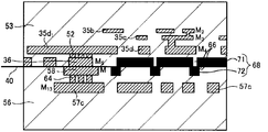
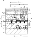
- FIG. 3 shows a first embodiment of a solid-state imaging device according to the present technology, that is, a back-illuminated CMOS solid-state imaging device.
- the back-illuminated CMOS solid-state imaging device is a CMOS solid-state imaging device having a light receiving portion disposed above the circuit portion and higher sensitivity and lower noise than the front-illuminated type.
- the first semiconductor chip unit 26 in which the pixel array 23 and the control circuit 24 are formed, and the logic circuit 25 are formed, similar to the solid-state imaging device 1a in FIG. 2A. It has a laminated semiconductor chip 32 to which the second semiconductor chip portion 28 is bonded. The first semiconductor chip portion 26 and the second semiconductor chip portion 28 are bonded so that the multilayer wiring layers described later face each other and the connection wirings are directly joined.
- the first semiconductor chip portion 26 is a two-dimensional array of a plurality of pixels comprising a photodiode PD serving as a photoelectric conversion portion and a plurality of pixel transistors Tr1 and Tr2 on a first semiconductor substrate 33 made of thinned silicon.
- An array of pixel arrays 34 is formed.
- a plurality of MOS transistors constituting the control circuit 24 are formed on the semiconductor substrate 33.
- a multilayer wiring layer 37 in which a plurality of, in this example, five wirings 35 [35a to 35d] and 36 made of metals M1 to M5 are arranged via an interlayer insulating film 53 is formed. .
- the wirings 35 and 36 are copper (Cu) wirings formed by a dual damascene method.
- a light shielding film 39 is formed including an optical black region 41 through an insulating film 38, and a color filter 44 and an on-semiconductor are formed on the effective pixel array 42 through a planarizing film 43.
- a chip lens 45 is formed.
- An on-semiconductor chip lens 45 can also be formed on the optical black region 41.
- the pixel transistors Tr1 and Tr2 are representative of a plurality of pixel transistors.
- FIG. 3 schematically shows the pixels of the pixel array 34, but FIG. 4 shows details of one pixel.
- the photodiode PD is formed on the thinned semiconductor substrate 33.
- the photodiode PD is formed, for example, having an n-type semiconductor region 46 and a P-type semiconductor region 47 on the substrate surface side.
- a P-type semiconductor region 48 is formed on the surface of the substrate constituting the pixel via a gate insulating film, and pixel transistors Tr1 and Tr2 are formed by the gate electrode 48 and a pair of source / drain regions 49.
- the pixel transistor Tr1 adjacent to the photodiode PD corresponds to the floating diffusion FD.
- Each unit pixel is separated by an element isolation region 51.
- the element isolation region 51 is formed, for example, in an STI (Shallow Trench Isolation) structure in which an insulating film such as a SiO 2 film is embedded in a groove formed in a substrate.
- the corresponding pixel transistor and the wiring 35, and the adjacent upper and lower wirings 35 are connected via the conductive via 52. Furthermore, the connection wiring 36 made of the fifth-layer metal M5 is formed facing the joint surface 40 with the second semiconductor chip portion 28. The connection wiring 36 is connected to a required wiring 35d of the fourth layer metal M4 through the conductive via 52.
- logic circuits 55 constituting peripheral circuits are formed in the regions to be the respective semiconductor chip portions of the second semiconductor substrate 54 made of silicon.
- the logic circuit 55 is formed by a plurality of MOS transistors Tr11 to Tr14 including CMOS transistors.
- wirings 57 [57a to 57c] and 58 of a plurality of layers, in this example, four layers of metals M11 to M14 are provided via an interlayer insulating film 56.
- the arranged multilayer wiring layer 59 is formed.
- the wirings 57 and 58 are copper (Cu) wirings by a dual damascene method.
- each MOS transistor Tr11, Tr12 has a gate electrode 62 in a semiconductor well region on the surface side of the second semiconductor substrate 54 via a pair of source / drain regions 61 and a gate insulating film. Formed.
- the MOS transistors Tr11 and Tr12 are isolated by, for example, an element isolation region 63 having an STI structure.
- the MOS transistors Tr11 to Tr14 and the wiring 57 and the adjacent upper and lower wirings 57 are connected through the conductive via 64. Furthermore, a connection wiring 58 made of the fourth layer metal M14 is formed facing the joint surface 40 with the first semiconductor chip portion 26. The connection wiring 58 is connected to a required wiring 57c of the third layer metal M13 through the conductive via 64.
- the first semiconductor chip portion 26 and the second semiconductor chip portion 28 are electrically connected by directly connecting the connection wirings 36 and 58 facing the bonding surface 40 so that the multilayer wiring layers 37 and 59 face each other. Connected to.
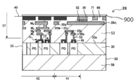
- the interlayer insulating film 66 in the vicinity of the junction is formed of a combination of a Cu diffusion barrier insulating film for preventing Cu diffusion of Cu wiring and an insulating film having no Cu diffusion barrier property, as will be described later in a manufacturing method. Direct connection of the connection wirings 36 and 58 by Cu wiring is performed by thermal diffusion bonding. Bonding between the interlayer insulating films 66 other than the connection wirings 36 and 58 is performed by plasma bonding or an adhesive.
- an extremely thin uniform insulating thin film 900 is formed on the surfaces of the multilayer wiring layers 37 and 59, and the plasma is formed. A method of joining by joining or the like is also possible.
- the insulating thin film 900 is not shown in FIG.
- a light shielding layer 68 is formed from the conductive film.
- the light shielding layer 68 of the present embodiment includes a light shielding portion (first conductor) 71 made of a metal M5 in the same layer as the connection wiring 36 on the first semiconductor chip portion 26 side, and a connection on the second semiconductor chip portion 28 side.
- the light shielding portion (second conductor) 72 is formed of the metal M14 in the same layer as the wiring 58.
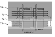
- FIG. 7A to FIG. 7C are configuration diagrams showing a light shielding portion of the solid-state imaging device of the present embodiment.
- the light shielding portions 71 of the present embodiment are formed in a layout arranged in a horizontal stripe shape having a plurality of openings 73 at a predetermined pitch when viewed from above.
- the width of the light shielding part 71 is wider than the width of the opening 73, but the width of the opening 73 may be wider than the width of the light shielding part 71.
- the light shielding portions 72 of the present embodiment are formed in a layout arranged in a horizontal stripe shape having a plurality of openings 74 at a predetermined pitch.
- the light shielding part 72 is formed at a position that closes the opening 73 of the light shielding part 71 and having a width wider than the width of the opening 73.
- the light shielding layer 68 after the light shielding portions 71 and 72 are joined is configured to overlap with the light shielding portions 71 and 72 being uniformly closed when viewed from above. That is, the area where the first conductor of the light shielding part 71 and the second conductor of the light shielding part 72 are formed is arranged in a size larger than the area where the pixel array 23 is formed.
- the width of the light shielding part 71 is formed wider than the width of the light shielding part 72, but the width of the light shielding part 72 may be formed wider than the width of the light shielding part 71.
- region of the joining surface 40 in which the conductor of the light-shielding part 71 and the light-shielding part 72 is formed can also have a clearance gap partially.
- the light shielding part 71 and the light shielding part 72 that closes the opening 73 are formed so as to partially overlap each other.
- the connection wirings 36 and 58 are directly joined, the light shielding parts 71 and 72 are directly joined at the overlapping portions at the same time.
- the light shielding portions 71 and 72 are formed such that one is a wiring having an opening 73 and the other is a shape covering the opening 73, has a larger area than the opening 73 and partially overlaps.
- the shape of the opening part 73 which concerns on this technique can consider various shapes, and is not restricted to the horizontal stripe shape of FIG. 7A.
- the light shielding layer 68 is preferably fixed at a potential, for example, a ground potential is applied to stabilize the potential.
- the potential can be fixed on the first semiconductor substrate 33 side, the second semiconductor substrate 54 side, or both.
- FIGS. 11 to 13 are steps on the side of the second semiconductor chip having the logic circuit
- FIGS. 14 to 16 are junctions. The subsequent steps are shown.
- a semiconductor well region 30 is formed in a region to be each semiconductor chip portion of a first semiconductor wafer (hereinafter referred to as a semiconductor substrate) 33 made of silicon, for example, and each pixel is formed in the semiconductor well region 30.
- a photodiode PD serving as a photoelectric conversion portion is formed.
- the element isolation region 51 (see FIG. 4) can be formed and placed first.
- Each photodiode PD is formed extending in the depth direction of the semiconductor well region 30.
- the photodiode PD is formed in the effective pixel array 42 and the optical black region 41 that constitute the pixel array 34.
- a plurality of pixel transistors constituting each pixel are formed on the surface 33a side of the semiconductor well region 30.
- the pixel transistor can be composed of, for example, a transfer transistor, a reset transistor, an amplification transistor, and a selection transistor.
- the pixel transistors Tr1 and Tr2 are shown as representatives.
- each of the pixel transistors Tr1 and Tr2 is formed to have a pair of source / drain regions and a gate electrode formed through a gate insulating film.
- wirings 35 [35a, 35b, 35c, 35d] made of a plurality of layers, in this example, four-layer metals M1 to M4 are provided via the interlayer insulating film 53, including the conductive vias 52.
- the wiring 35 can be formed by a dual damascene method. That is, via-first connection holes and wiring grooves are simultaneously formed in the interlayer insulating film 53, a Cu diffusion barrier metal film and a Cu seed film for preventing Cu diffusion are formed, and then a Cu material layer is embedded by plating.
- the Cu diffusion barrier metal film include Ta, TaN, Ti, TiN, W, WN, Ru, TiZrN, and alloy films containing these.
- an excessive Cu material layer is removed by a CMP (Chemical Mechanical Polishing) method, and a Cu wiring integrated with the planarized conductive via is formed. Thereafter, although not shown, a Cu diffusion barrier insulating film is formed.
- a Cu diffusion barrier insulating film for example, an insulating film such as SiN, SiC, siCN, or SiON can be used. By repeating this process, wirings 35a to 35d made of four layers of metals M1 to M4 are formed.
- a first insulating film 76 not having a Cu diffusion barrier property, a second insulating film 77 not having a Cu diffusion barrier property, and a Cu diffusion barrier insulating film 75 are sequentially formed.
- the first insulating film 76 and the second insulating film 77 are formed of a SiO2 film, a SiCOH film, or the like.
- As the Cu barrier insulating film 75 for example, an insulating film such as SiN, SiC, SiCN, or SiON can be used as described above.
- the Cu diffusion barrier insulating film 75, the first insulating film 76, and the second insulating film 77 correspond to the interlayer insulating film 53.
- the Cu diffusion barrier insulating film 75, the second insulating film 77, and the first insulating film 76 on the outermost surface are patterned to selectively form via holes 80.
- the second insulating film 77 is patterned to selectively form an opening 78. That is, patterning is performed so as to have an opening 78 in a portion corresponding to the light shielding portion 71 (portion excluding the opening 73) to be formed, an opening 79 in a portion corresponding to the connection wiring 36 to be formed, and a via hole 80. .
- the light shielding part 71 having the opening 73 by embedding the Cu material in the openings 78 and 79 and the via hole 80 using the dual damascene method Conductive vias 52 and connection wirings 36 connected to the wirings 35d are formed.
- the light shielding portion 71 and the connection wiring 36 are formed of the fifth layer metal M5.
- the multilayer wiring layer 37 is formed by the wirings 35a to 35d made of the metals M1 to M5, the connection wiring 36, the light shielding portion 71, the interlayer insulating film 53, and the insulating films 75 to 77.
- the wiring 35d1 of the four layers of metal M4 connected to the connection wiring 36 is sufficiently extended to the light shielding part 71 side so that the emitted light from the logic circuit side does not leak to the photodiode PD side. It is preferable to form in an area overlapping with 71.
- an extremely thin uniform insulating thin film 900 is formed on the light shielding part 71 and the connection wiring 36.
- a semiconductor well region 50 is formed in a region to be each semiconductor chip portion of a second semiconductor wafer (hereinafter referred to as a semiconductor substrate) 54 made of silicon.
- a plurality of MOS transistors Tr11 to Tr14 constituting the logic circuit 55 are formed in the semiconductor well region 50.
- the MOS transistors Tr11 to Tr14 are shown as representatives.
- the element isolation region 63 (see FIG. 5) can be formed and placed first.
- a plurality of layers, in this example, three layers of metal M11 to M13, wirings 57 [57a, 57b, 57c] including conductive vias 64 are formed on the upper surface side of the semiconductor substrate 54 via an interlayer insulating film 56.
- the wiring 57 can be formed by a dual damascene method. In other words, via-first connection holes and wiring grooves are simultaneously formed in the interlayer insulating film, a Cu diffusion barrier metal film and a Cu seed film for preventing Cu diffusion are formed, and then a Cu material layer is embedded by plating.
- the Cu diffusion barrier metal film include Ta, TaN, Ti, TiN, W, WN, Ru, TiZrN, and alloy films containing these.
- an excessive Cu material layer is removed by a CMP (Chemical Mechanical Polishing) method, and a Cu wiring integrated with the planarized conductive via is formed. Thereafter, although not shown, a Cu diffusion barrier insulating film is formed.
- a Cu diffusion barrier insulating film for example, an insulating film such as SiN, SiC, siCN, or SiON can be used.
- a first insulating film 82 not having a Cu diffusion barrier property, a second insulating film 83 not having a Cu diffusion barrier property, and a Cu diffusion barrier insulating film 81 are sequentially formed.
- the first insulating film 82 and the second insulating film 83 are formed of a SiO2 film, a SiCOH film, or the like.
- As the Cu barrier insulating film 81 for example, an insulating film such as SiN, SiC, SiCN, or SiON can be used as described above.
- the Cu diffusion barrier insulating film 81, the first insulating film 82, and the second insulating film 83 correspond to an interlayer insulating film.
- the via diffusion is first performed using lithography and etching techniques, and the Cu diffusion barrier insulating film 81, the second insulating film 83, and the first insulating film 82 on the outermost surface are patterned to selectively form via holes 86.
- the second insulating film 83 is patterned to selectively form openings 84 and 85.
- the opening 84 is formed at a position that covers the opening 73 of the light shielding part 71 on the first semiconductor chip side.
- the opening 84 covers the opening 73 of the light shielding part 71 and partially overlaps the light shielding part 71 so that light leakage due to misalignment does not occur when the first semiconductor substrate and the second semiconductor substrate are bonded later. It is desirable to form in a size. That is, patterning is performed so as to have a portion of the opening 84 corresponding to the light shielding portion 72 to be formed, a portion of the opening 85 corresponding to the connection wiring 58 to be formed, and the via hole 86.
- a Cu material is embedded in the openings 84 and 85 and the via hole 86 using the dual damascene method to connect to the light shielding portion 72 and the wiring 57c.
- Conductive vias 64 and connection wirings 58 are formed.
- the light shielding portion 72 and the connection wiring 58 are formed of the fourth layer metal M14.
- a multilayer wiring layer 59 is formed by the wirings 57a to 57c, the connection wiring 58, the light shielding portion 72, the interlayer insulating film 56, and the insulating films 81 to 83 made of the metals M11 to M13.
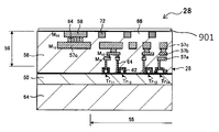
- an extremely thin uniform insulating thin film 901 is formed on the light shielding portion 72 and the connection wiring 58.
- the first semiconductor substrate 33 and the second semiconductor substrate 54 are electrically connected to each other with the multilayer wiring layers facing each other and the connection wirings 36 and 58 are in direct contact with each other.
- the first semiconductor substrate 33 and the second semiconductor substrate 54 are bonded. That is, the first and second semiconductor substrates 33 and 54 are physically joined and electrically connected.
- the light shielding part 71 and the light shielding part 72 are also directly joined at the overlapping portion. That is, the connection wirings 36 and 58 and the light shielding portions 71 and 72 are thermally diffused and bonded by heat treatment.
- the heat treatment temperature at this time can be about 100 ° C. to 500 ° C.
- the insulating films that are interlayer insulating films are subjected to surface treatment to perform plasma bonding. Note that the insulating films which are interlayer insulating films can be bonded to each other with an adhesive.
- the first conductor of the light shielding portion 71 and the second conductor of the light shielding portion 72 are made of copper which is a conductor by first sandwiching an insulating film between the bonding surfaces 40 and then applying heat. Are connected in the vicinity of the joint surface 40. Therefore, the first conductor and the second conductor are arranged closer to the bonding surface 40 than the logic circuit 55 and the wiring 35 formed in the first semiconductor chip 26 and the second semiconductor chip, respectively.
- the first semiconductor substrate 33 is thinned by grinding and polishing using a CMP method or the like so that the required film thickness of the photodiode PD remains from the back side.
- a light shielding film 39 is formed on the thinned surface through the insulating film 38 so as to cover the photodiode PD corresponding to the optical black region. Further, the color filter 44 and the on-semiconductor chip lens 45 are formed on the photodiode PD corresponding to the effective pixel array via the planarizing film 43.
- a semiconductor chip is formed by separating the bonded first semiconductor substrate 33 and second semiconductor substrate s54 into respective semiconductor chips, and the target solid-state imaging device 31 shown in FIG. 3 is obtained.
- a material having high conductivity, high light shielding properties, and easy joining is desirable.
- a material having such properties in addition to Cu, a single material such as Al, W, Ti, Ta, Mo, Ru, or an alloy can be used.
- the film thickness of the light shielding layer 68 in this example, the film thickness of the light shielding parts 71 and 72, is desirably determined according to the wavelength of light on the second semiconductor chip part 28 side that emits light.
- the thickness of the light shielding layer 68, and hence the thickness of the light shielding portions 71 and 72 can be about 50 nm to 800 nm.
- the first conductor 71 and the second conductor are formed in the vicinity of the joint surface 40 between the first semiconductor chip unit 26 and the second semiconductor chip unit 28.
- the light shielding layer 68 and the shield layer against electrical noise are formed only by the conductor 72.
- the first conductor 71 has a higher area ratio in contact with the joint surface 40 than the second conductor 72 and is asymmetric. For this reason, according to the solid-state imaging device 31 and the manufacturing method thereof, it is possible to realize wafer bonding of a conductive film having a high area ratio and suppress generation of voids on the bonding surface 40.
- the solid-state imaging device 31 that improves the image quality by suppressing the generation of voids on the joint surface 40.
- the area ratio in contact with the bonding surface 40 may be an asymmetrical difference between the first conductor 71 and the second conductor 72, and the second conductor 72 is more than the first conductor 71. It may be high.
- asymmetric means a layout in which the Cu area ratio on the lower substrate side is 30% or less and the Cu area ratio on the upper substrate is 70% or more, and 100% can be shielded from light after bonding.
- the area ratio of the higher substrate is desirably 70% or more, and more preferably 87% or more.
- the area ratio of the lower substrate is desirably 30% or less, and more preferably 13% or less.
- a dummy conductor may be disposed in the vicinity of the bonding surface 40 instead of the first conductor 71 or the second conductor 72.
- the metal M5 in the same layer as the connection wirings 36 and 58 near the junction between the first semiconductor chip unit 26 and the second semiconductor chip unit 28. , M14 is formed.
- the light shielding layer 68 can suppress light emitted by hot carriers from the MOS transistor of the logic circuit 55 of the second semiconductor chip unit 28 from entering the pixel array on the first semiconductor chip unit 26 side. Therefore, the adverse effect of light emission due to hot carriers is suppressed, so that dark current and random noise can be suppressed.
- the light shielding layer 68 is formed of the same metal M5 and M14 as the connection wirings 36 and 58, the bonded semiconductor compared to the prior art.
- the thickness of the entire chip can be reduced, and the solid-state imaging device 31 can be made thinner.
- the solid-state imaging device 31 with less dark current and random noise can be provided without increasing the thickness of the entire semiconductor chip.
- the wiring, the connection wiring, and the light shielding layer can be formed at the same time. It is possible to manufacture a solid-state imaging device with low dark current and random noise at low cost.
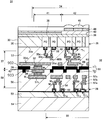
- Solid-State Imaging Device of Second Embodiment> A second embodiment of the solid-state imaging device according to the present technology will be described with reference to FIG. This embodiment is different from the first embodiment of FIG. 16 in that the connection wiring 36 and the wiring 57c of the metal M13 are connected by the light shielding portion 72 without forming the conductive via 64 of the wiring layer 58 and the light shielding portion 72. This is the point of connection.
- the solid-state imaging device 31 of the present embodiment has the same effect as the solid-state imaging device 31 of the first embodiment, and further has an advantage that the manufacturing process and the manufacturing cost can be reduced by not forming the conductive via 64. is there.
- Solid-State Imaging Device of Third Embodiment> A third embodiment of the solid-state imaging device according to the present technology will be described with reference to FIG. This embodiment is different from the first embodiment of FIG. 16 in that the wiring area ratio of the wiring 902 is set in the same manner as the light shielding layer 68 even when the connection wiring 36 and the wiring 58 are used as power supply wiring. The wiring area ratio of the wiring 903 is lowered and the wirings 902 and 903 are joined asymmetrically.
- the solid-state imaging device 31 of the present embodiment also has the same effect as the solid-state imaging device 31 of the first embodiment, and in particular, the area ratio of the wirings 902 and 903 in addition to the light shielding layer 68 is asymmetrical, and the other area By increasing the ratio, voids generated at the time of joining can be further suppressed.
- Solid-State Imaging Device of Fourth Embodiment> A fourth embodiment of the solid-state imaging device according to the present technology will be described with reference to FIG. This embodiment is different from the first embodiment of FIG. 16 in that two layers of the second semiconductor substrate 54 are stacked in the second semiconductor chip portion 28. In the interlayer insulating film and the second semiconductor substrate 54 bonded to the interlayer insulating film, the wirings 57 c are electrically connected to each other through the wiring 904.
- the solid-state imaging device 31 of this embodiment also has the same effect as the solid-state imaging device 31 of the first embodiment. Note that the stack of the semiconductor substrates of the solid-state imaging device according to the present technology is not limited to three layers or less, and may be four layers or more.
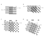
- Solid-State Imaging Device of Fifth Embodiment> A fifth embodiment of the solid-state imaging device according to the present technology will be described with reference to FIGS. 20 to 22. This embodiment is different from the first embodiment of FIG. 16 in that the planar layout of the light shielding layer 68 is arranged in an oblique stripe type or a checkered type other than the horizontal stripe type shown in FIG. It is.
- FIG. 20A shows a case where the planar shape of the light shielding layer 68 is a horizontal stripe type similar to that of the first embodiment.
- variety of each vertical direction of the light shielding parts 71 and 72 may be the same, and may differ.
- FIG. 20B shows a case where the planar shape of the light shielding layer 68 is an oblique stripe type arranged from the upper left to the lower right.
- FIG. 20C shows a case where the planar shape of the light shielding layer 68 is a checkered pattern. In this checkered pattern, a plurality of rectangular light shielding portions 72 having a larger area than the opening 73 are arranged so as to cover the plurality of rectangular openings 73 formed in the light shielding portion 71. Note that the rectangle includes a square.
- FIG. 20D shows a case where the planar shape of the light shielding layer 68 is an oblique checkered pattern obtained by rotating the checkered pattern of FIG. 20C by a predetermined angle in the clockwise
- FIG. 21 is an enlarged view showing a signal line layout of the pixel array of the solid-state imaging device of the present embodiment.
- a plurality of photodiodes are arranged in parallel in the vertical and horizontal directions.
- a plurality of reset signal lines M21, transfer signal lines M22, and pixel selection signal lines M23 are horizontally arranged at predetermined pitches in the horizontal direction.
- a plurality of vertical signal lines M3 are vertically arranged at a predetermined pitch in the vertical direction.
- 22A to 22C are configuration diagrams for explaining the layout of the shield layer of the solid-state imaging device according to the present embodiment.
- the light shielding layer (shield layer) 68 shown in FIG. 22A is arranged in a vertical stripe type in which light shielding portions 71 and 72 have a plurality of openings 73 and 74 at a predetermined pitch when viewed from above.
- a difference occurs between the vertical signal lines M3 and the shield layer 68, and the total capacity of each vertical signal line M3 may vary.
- the shield layer 68 shown in FIG. 22B has light shielding portions 71 and 72 arranged in a horizontal stripe shape having a plurality of openings 73 and 74 at a predetermined pitch when viewed from above.
- a difference occurs between the horizontal control lines M21 to M23 and the shield layer 68, and the total capacity of the horizontal signal lines M21 to M23 may vary.
- the light shielding portions 71 and 72 are arranged in an oblique stripe shape having a plurality of openings 73 at a predetermined pitch from the upper left to the lower right as viewed from above.
- the interlayer capacitance between each vertical signal line M3 and the shield layer 68 per horizontal control line M21 to M23 is uniform, and the total capacitance It becomes possible to suppress the variation of. Therefore, the band noise of the solid-state imaging device can be further reduced as compared with other vertical and horizontal stripe types.
- the pitch repeat direction of the stripe-type or checkered-type shield layer 68 is arranged obliquely with respect to the horizontal signal lines M21 to M3 and the vertical signal lines M3 of the logic circuit 55. Since the capacitance between the shield layer 68 and each signal line can be made uniform throughout the pixel array 23, the electrical noise of the solid-state imaging device 31 can be reduced. Furthermore, as a countermeasure against reflection, the influence of capacitive coupling can be dispersed by arranging the shield layer 68 in an oblique stripe shape so as not to be orthogonal to all signal lines.
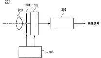
- FIG. 23 is a diagram illustrating an electronic apparatus according to the present technology.
- the above-described solid-state imaging device according to the present technology can be applied to electronic devices such as a camera system such as a digital camera or a video camera, a mobile phone having an imaging function, or other devices having an imaging function. .
- FIG. 23 shows a sixth embodiment applied to a camera as an example of an electronic apparatus according to the present technology.
- the camera according to the present embodiment is an example of a video camera capable of capturing still images or moving images.
- a camera 201 according to this embodiment includes a solid-state imaging device 202, an optical system 203 that guides incident light to a light receiving sensor unit of the solid-state imaging device 202, and a shutter device 204. Furthermore, a drive circuit 205 that drives the solid-state imaging device 202 and a signal processing circuit 206 that processes an output signal of the solid-state imaging device 202 are included.
- the optical system (optical lens) 203 forms image light (incident light) from the subject on the imaging surface of the solid-state imaging device 202. Thereby, signal charges are accumulated in the solid-state imaging device 202 for a certain period.
- the optical system 203 may be an optical lens system including a plurality of optical lenses.
- the shutter device 204 controls a light irradiation period and a light shielding period for the solid-state imaging device 202.
- the drive circuit 205 supplies a drive signal that controls the transfer operation of the solid-state imaging device 202 and the shutter operation of the shutter device 204.
- Signal transfer of the solid-state imaging device 202 is performed by a drive signal (timing signal) supplied from the drive circuit 205.
- the signal processing circuit 206 performs various signal processing.
- the video signal subjected to the signal processing is stored in a storage medium such as a memory or output to a monitor.
- the back-illuminated solid-state imaging device 202 since the back-illuminated solid-state imaging device 202 according to the present technology described above is provided, the light emitted from the hot carrier from the MOS transistor of the logic circuit is not incident on the pixel array side. , Dark current and random noise can be suppressed. Therefore, a high-quality electronic device can be provided. For example, a camera with improved image quality can be provided.
- this technique can take the following structures.
- the solid-state imaging device according to (1) wherein a wiring and a connection hole for fixing the potential of the first conductor and the second conductor are formed in the second semiconductor chip. .
- the first conductor and the second conductor are disposed closer to the bonding surface than the logic circuit and the wiring formed in the first semiconductor chip and the second semiconductor chip, respectively.
- (9) The solid-state imaging device according to (1), wherein the area where the first conductor and the second conductor are formed is arranged in a size larger than the area where the pixel array is formed. .
- a plurality of the first conductors and the second conductors are formed, and an arrangement direction of the plurality of first conductors and the plurality of second conductors is determined by the first semiconductor chip and The solid-state imaging device according to (1), wherein the solid-state imaging device has a direction inclined with respect to a direction of a signal line of an analog circuit formed on the second semiconductor chip.
- a first semiconductor chip on which one or a plurality of first conductors and a pixel array are formed; And at least a second semiconductor chip bonded to the first semiconductor chip and having one or more second conductors and logic circuits formed thereon, The first conductor and the second conductor are overlapped and electrically connected at a joint surface between the first semiconductor chip and the second semiconductor chip,
- An electronic apparatus comprising a solid-state imaging device having an area in contact with the bonding surface that is different between the first conductor and the second conductor.
- Solid-state imaging device Pixel 3, 23, 34 Pixel array (pixel region) 4 vertical drive circuit 5 column signal processing circuit 6 horizontal drive circuit 7 output circuit 8, 24, 24-1, 24-2 control circuit 9 vertical signal line 10 horizontal signal line 21, 33 first semiconductor substrate 22, 54 second Semiconductor substrate 25, 55 Logic circuit 26 First semiconductor chip portion 28 Second semiconductor chip portion 30, 50 Semiconductor well region 32 Multilayer semiconductor chip 33a Surfaces 35a-35d, 36, 57a-57c, 58, 902-904 Wiring 37, 59 Multi-layer wiring layer 38 Insulating film 39 Shading film 40 Bonding surface 41 Optical black region 42 Effective pixel array 43 Flattening film 44 Color filter 45 On-semiconductor chip lens 47, 48 P-type semiconductor region 49, 61 Source / drain region 51 , 63 Element isolation regions 52, 64 Conductive vias 53, 56, 66 Interlayer insulating film 62 Gate electrode 68 Light-shielding layer 71 Light-shielding part (first conductor) 72 Light-shield
Landscapes
- Engineering & Computer Science (AREA)
- Multimedia (AREA)
- Signal Processing (AREA)
- Solid State Image Pick-Up Elements (AREA)
- Transforming Light Signals Into Electric Signals (AREA)
- Internal Circuitry In Semiconductor Integrated Circuit Devices (AREA)
Abstract
L'invention concerne un dispositif de prise de vue à semi-conducteurs, dans lequel, dans une surface de liaison entre une pluralité de puces semi-conductrices, une liaison de tranche de films conducteurs est obtenue au niveau d'un rapport de surface élevé, et la génération de vides peut être supprimée. Un dispositif de prise de vue à semi-conducteurs (31) comprend au moins : une première puce semi-conductrice (26) dans laquelle un ou plusieurs premiers corps conducteurs (71) et un réseau de pixels (34) sont formés ; et une seconde section de puce semi-conductrice (28), qui est connectée à la première puce semi-conductrice (26), et dans laquelle un ou plusieurs seconds corps conducteurs (72) et un circuit logique (55) sont formés. Au niveau d'une surface de liaison (40) entre la première puce semi-conductrice (26) et la seconde section de puce semi-conductrice, le premier corps conducteur (71) et le second corps conducteur (72) se chevauchent et sont électriquement connectés l'un à l'autre, et une zone de premier corps conducteur (71) en contact avec la surface de liaison (40), et une zone de second corps conducteur (72) en contact avec la surface de liaison sont différentes l'une de l'autre.
Priority Applications (4)
| Application Number | Priority Date | Filing Date | Title |
|---|---|---|---|
| CN201780011297.3A CN108701697B (zh) | 2016-03-30 | 2017-03-03 | 固态图像传感器、固态图像传感器的制造方法以及电子设备 |
| JP2018508850A JP6885393B2 (ja) | 2016-03-30 | 2017-03-03 | 固体撮像装置、固体撮像装置の製造方法および電子機器 |
| US16/086,362 US20190115387A1 (en) | 2016-03-30 | 2017-03-03 | Solid-state image sensor, method for producing solid-state image sensor, and electronic device |
| US17/861,982 US12520614B2 (en) | 2016-03-30 | 2022-07-11 | Solid-state image sensor, method for producing solid-state image sensor, and electronic device |
Applications Claiming Priority (2)
| Application Number | Priority Date | Filing Date | Title |
|---|---|---|---|
| JP2016069624 | 2016-03-30 | ||
| JP2016-069624 | 2016-03-30 |
Related Child Applications (2)
| Application Number | Title | Priority Date | Filing Date |
|---|---|---|---|
| US16/086,362 A-371-Of-International US20190115387A1 (en) | 2016-03-30 | 2017-03-03 | Solid-state image sensor, method for producing solid-state image sensor, and electronic device |
| US17/861,982 Continuation US12520614B2 (en) | 2016-03-30 | 2022-07-11 | Solid-state image sensor, method for producing solid-state image sensor, and electronic device |
Publications (1)
| Publication Number | Publication Date |
|---|---|
| WO2017169505A1 true WO2017169505A1 (fr) | 2017-10-05 |
Family
ID=59964012
Family Applications (1)
| Application Number | Title | Priority Date | Filing Date |
|---|---|---|---|
| PCT/JP2017/008404 Ceased WO2017169505A1 (fr) | 2016-03-30 | 2017-03-03 | Dispositif de prise de vue à semi-conducteurs, procédé de fabrication de dispositif de prise de vue à semi-conducteurs et appareil électronique |
Country Status (4)
| Country | Link |
|---|---|
| US (2) | US20190115387A1 (fr) |
| JP (1) | JP6885393B2 (fr) |
| CN (1) | CN108701697B (fr) |
| WO (1) | WO2017169505A1 (fr) |
Cited By (9)
| Publication number | Priority date | Publication date | Assignee | Title |
|---|---|---|---|---|
| CN110401803A (zh) * | 2018-04-25 | 2019-11-01 | 株式会社东芝 | 固体摄像元件 |
| WO2019235400A1 (fr) * | 2018-06-05 | 2019-12-12 | ソニーセミコンダクタソリューションズ株式会社 | Dispositif d'imagerie à semi-conducteur, son procédé de production et dispositif électronique |
| JP2020054640A (ja) * | 2018-10-02 | 2020-04-09 | パナソニックi−PROセンシングソリューションズ株式会社 | 内視鏡 |
| WO2020158216A1 (fr) * | 2019-01-28 | 2020-08-06 | ソニーセミコンダクタソリューションズ株式会社 | Dispositif d'imagerie à semi-conducteurs et appareil électronique |
| JP2021019059A (ja) * | 2019-07-18 | 2021-02-15 | キヤノン株式会社 | 固体撮像素子 |
| JP2021064711A (ja) * | 2019-10-15 | 2021-04-22 | ソニーセミコンダクタソリューションズ株式会社 | 撮像装置 |
| WO2021095420A1 (fr) * | 2019-11-11 | 2021-05-20 | ソニーセミコンダクタソリューションズ株式会社 | Dispositif à semi-conducteur et dispositif électronique |
| JP2023079055A (ja) * | 2021-11-26 | 2023-06-07 | キヤノン株式会社 | 光電変換装置、光電変換システム、移動体、および、光電変換装置の設計方法 |
| US20230361145A1 (en) * | 2018-10-05 | 2023-11-09 | Sony Semiconductor Solutions Corporation | Semiconductor device, method of manufacturing semiconductor device, and imaging element |
Families Citing this family (13)
| Publication number | Priority date | Publication date | Assignee | Title |
|---|---|---|---|---|
| JP6465545B2 (ja) | 2013-09-27 | 2019-02-06 | ソニー株式会社 | 撮像素子およびその製造方法ならびに電子機器 |
| CN108701697B (zh) | 2016-03-30 | 2022-12-16 | 索尼公司 | 固态图像传感器、固态图像传感器的制造方法以及电子设备 |
| JP6661506B2 (ja) * | 2016-09-23 | 2020-03-11 | サムスン エレクトロニクス カンパニー リミテッド | 固体撮像装置 |
| JP2018064758A (ja) * | 2016-10-19 | 2018-04-26 | ソニーセミコンダクタソリューションズ株式会社 | 半導体装置、製造方法、および電子機器 |
| WO2020116040A1 (fr) | 2018-12-04 | 2020-06-11 | ソニーセミコンダクタソリューションズ株式会社 | Dispositif à semi-conducteur et dispositif électronique |
| US11482556B2 (en) * | 2019-02-15 | 2022-10-25 | Taiwan Semiconductor Manufacturing Company, Ltd. | Low-noise image sensor having stacked semiconductor substrates |
| CN110505419B (zh) * | 2019-08-27 | 2022-04-15 | Oppo广东移动通信有限公司 | 一种像素结构、图像传感器及终端 |
| US12356752B2 (en) * | 2020-01-06 | 2025-07-08 | Sony Semiconductor Solutions Corporation | Light-receiving device |
| CN111968959A (zh) * | 2020-08-06 | 2020-11-20 | 长江存储科技有限责任公司 | 半导体器件及其制作方法 |
| CN112310135B (zh) * | 2020-10-19 | 2024-02-06 | 锐芯微电子股份有限公司 | 传感器结构和传感器结构的形成方法 |
| JP2022144050A (ja) * | 2021-03-18 | 2022-10-03 | ソニーセミコンダクタソリューションズ株式会社 | 撮像装置 |
| KR102895932B1 (ko) | 2021-08-05 | 2025-12-03 | 삼성전자주식회사 | 이미지 센서 |
| CN116130499A (zh) * | 2022-05-31 | 2023-05-16 | 神盾股份有限公司 | 光感测单元及光感测装置 |
Citations (2)
| Publication number | Priority date | Publication date | Assignee | Title |
|---|---|---|---|---|
| JP2012164870A (ja) * | 2011-02-08 | 2012-08-30 | Sony Corp | 固体撮像装置とその製造方法、及び電子機器 |
| WO2012161044A1 (fr) * | 2011-05-24 | 2012-11-29 | ソニー株式会社 | Dispositif à semi-conducteurs |
Family Cites Families (8)
| Publication number | Priority date | Publication date | Assignee | Title |
|---|---|---|---|---|
| KR100610481B1 (ko) | 2004-12-30 | 2006-08-08 | 매그나칩 반도체 유한회사 | 수광영역을 넓힌 이미지센서 및 그 제조 방법 |
| TWI513301B (zh) * | 2010-06-02 | 2015-12-11 | 新力股份有限公司 | 半導體裝置,固態成像裝置及相機系統 |
| JP2014022561A (ja) | 2012-07-18 | 2014-02-03 | Sony Corp | 固体撮像装置、及び、電子機器 |
| US9230941B2 (en) | 2014-03-28 | 2016-01-05 | Taiwan Semiconductor Manufacturing Company, Ltd. | Bonding structure for stacked semiconductor devices |
| JP6079807B2 (ja) * | 2015-03-24 | 2017-02-15 | ソニー株式会社 | 固体撮像装置及び電子機器 |
| KR102423813B1 (ko) * | 2015-11-27 | 2022-07-22 | 삼성전자주식회사 | 반도체 소자 |
| CN106876419B (zh) | 2015-12-10 | 2019-07-30 | 中芯国际集成电路制造(上海)有限公司 | Cmos图像传感器及其形成方法 |
| CN108701697B (zh) | 2016-03-30 | 2022-12-16 | 索尼公司 | 固态图像传感器、固态图像传感器的制造方法以及电子设备 |
-
2017
- 2017-03-03 CN CN201780011297.3A patent/CN108701697B/zh active Active
- 2017-03-03 WO PCT/JP2017/008404 patent/WO2017169505A1/fr not_active Ceased
- 2017-03-03 JP JP2018508850A patent/JP6885393B2/ja not_active Expired - Fee Related
- 2017-03-03 US US16/086,362 patent/US20190115387A1/en not_active Abandoned
-
2022
- 2022-07-11 US US17/861,982 patent/US12520614B2/en active Active
Patent Citations (2)
| Publication number | Priority date | Publication date | Assignee | Title |
|---|---|---|---|---|
| JP2012164870A (ja) * | 2011-02-08 | 2012-08-30 | Sony Corp | 固体撮像装置とその製造方法、及び電子機器 |
| WO2012161044A1 (fr) * | 2011-05-24 | 2012-11-29 | ソニー株式会社 | Dispositif à semi-conducteurs |
Cited By (13)
| Publication number | Priority date | Publication date | Assignee | Title |
|---|---|---|---|---|
| CN110401803A (zh) * | 2018-04-25 | 2019-11-01 | 株式会社东芝 | 固体摄像元件 |
| WO2019235400A1 (fr) * | 2018-06-05 | 2019-12-12 | ソニーセミコンダクタソリューションズ株式会社 | Dispositif d'imagerie à semi-conducteur, son procédé de production et dispositif électronique |
| US12199121B2 (en) | 2018-06-05 | 2025-01-14 | Sony Semiconductor Solutions Corporation | Solid-state imaging device with increased bonding strength, and method of manufacturing the solid-state imaging device |
| JP7376057B2 (ja) | 2018-10-02 | 2023-11-08 | i-PRO株式会社 | 内視鏡 |
| JP2020054640A (ja) * | 2018-10-02 | 2020-04-09 | パナソニックi−PROセンシングソリューションズ株式会社 | 内視鏡 |
| US12199123B2 (en) * | 2018-10-05 | 2025-01-14 | Sony Semiconductor Solutions Corporation | Semiconductor device including a structure for higher integration |
| US20230361145A1 (en) * | 2018-10-05 | 2023-11-09 | Sony Semiconductor Solutions Corporation | Semiconductor device, method of manufacturing semiconductor device, and imaging element |
| WO2020158216A1 (fr) * | 2019-01-28 | 2020-08-06 | ソニーセミコンダクタソリューションズ株式会社 | Dispositif d'imagerie à semi-conducteurs et appareil électronique |
| JP2021019059A (ja) * | 2019-07-18 | 2021-02-15 | キヤノン株式会社 | 固体撮像素子 |
| JP2021064711A (ja) * | 2019-10-15 | 2021-04-22 | ソニーセミコンダクタソリューションズ株式会社 | 撮像装置 |
| US12543398B2 (en) | 2019-10-15 | 2026-02-03 | Sony Semiconductor Solutions Corporation | Imaging device |
| WO2021095420A1 (fr) * | 2019-11-11 | 2021-05-20 | ソニーセミコンダクタソリューションズ株式会社 | Dispositif à semi-conducteur et dispositif électronique |
| JP2023079055A (ja) * | 2021-11-26 | 2023-06-07 | キヤノン株式会社 | 光電変換装置、光電変換システム、移動体、および、光電変換装置の設計方法 |
Also Published As
| Publication number | Publication date |
|---|---|
| US20220415956A1 (en) | 2022-12-29 |
| CN108701697A (zh) | 2018-10-23 |
| JP6885393B2 (ja) | 2021-06-16 |
| US20190115387A1 (en) | 2019-04-18 |
| CN108701697B (zh) | 2022-12-16 |
| JPWO2017169505A1 (ja) | 2019-02-14 |
| US12520614B2 (en) | 2026-01-06 |
Similar Documents
| Publication | Publication Date | Title |
|---|---|---|
| JP6885393B2 (ja) | 固体撮像装置、固体撮像装置の製造方法および電子機器 | |
| TWI757433B (zh) | 固態影像感測器,製造固態影像感測器之方法,以及電子器件 | |
| KR101942680B1 (ko) | 반도체 장치 및 전자 기기 | |
| JP5696513B2 (ja) | 固体撮像装置とその製造方法、及び電子機器 | |
| WO2018116559A1 (fr) | Dispositif d'imagerie à semi-conducteurs, procédé de fabrication de dispositif d'imagerie à semi-conducteurs, et appareil électronique | |
| US12261187B2 (en) | Semiconductor device |
Legal Events
| Date | Code | Title | Description |
|---|---|---|---|
| WWE | Wipo information: entry into national phase |
Ref document number: 2018508850 Country of ref document: JP |
|
| NENP | Non-entry into the national phase |
Ref country code: DE |
|
| 121 | Ep: the epo has been informed by wipo that ep was designated in this application |
Ref document number: 17774050 Country of ref document: EP Kind code of ref document: A1 |
|
| 122 | Ep: pct application non-entry in european phase |
Ref document number: 17774050 Country of ref document: EP Kind code of ref document: A1 |