WO2017169719A1 - Élément d'imagerie à semi-conducteurs et appareil électronique - Google Patents
Élément d'imagerie à semi-conducteurs et appareil électronique Download PDFInfo
- Publication number
- WO2017169719A1 WO2017169719A1 PCT/JP2017/010103 JP2017010103W WO2017169719A1 WO 2017169719 A1 WO2017169719 A1 WO 2017169719A1 JP 2017010103 W JP2017010103 W JP 2017010103W WO 2017169719 A1 WO2017169719 A1 WO 2017169719A1
- Authority
- WO
- WIPO (PCT)
- Prior art keywords
- photoelectric conversion
- light
- state imaging
- solid
- imaging device
- Prior art date
- Legal status (The legal status is an assumption and is not a legal conclusion. Google has not performed a legal analysis and makes no representation as to the accuracy of the status listed.)
- Ceased
Links
Images




Classifications
-
- H—ELECTRICITY
- H10—SEMICONDUCTOR DEVICES; ELECTRIC SOLID-STATE DEVICES NOT OTHERWISE PROVIDED FOR
- H10F—INORGANIC SEMICONDUCTOR DEVICES SENSITIVE TO INFRARED RADIATION, LIGHT, ELECTROMAGNETIC RADIATION OF SHORTER WAVELENGTH OR CORPUSCULAR RADIATION
- H10F39/00—Integrated devices, or assemblies of multiple devices, comprising at least one element covered by group H10F30/00, e.g. radiation detectors comprising photodiode arrays
- H10F39/10—Integrated devices
- H10F39/12—Image sensors
- H10F39/191—Photoconductor image sensors
- H10F39/192—Colour image sensors
-
- H—ELECTRICITY
- H10—SEMICONDUCTOR DEVICES; ELECTRIC SOLID-STATE DEVICES NOT OTHERWISE PROVIDED FOR
- H10F—INORGANIC SEMICONDUCTOR DEVICES SENSITIVE TO INFRARED RADIATION, LIGHT, ELECTROMAGNETIC RADIATION OF SHORTER WAVELENGTH OR CORPUSCULAR RADIATION
- H10F39/00—Integrated devices, or assemblies of multiple devices, comprising at least one element covered by group H10F30/00, e.g. radiation detectors comprising photodiode arrays
- H10F39/10—Integrated devices
- H10F39/12—Image sensors
- H10F39/18—Complementary metal-oxide-semiconductor [CMOS] image sensors; Photodiode array image sensors
- H10F39/182—Colour image sensors
-
- H—ELECTRICITY
- H04—ELECTRIC COMMUNICATION TECHNIQUE
- H04N—PICTORIAL COMMUNICATION, e.g. TELEVISION
- H04N25/00—Circuitry of solid-state image sensors [SSIS]; Control thereof
- H04N25/70—SSIS architectures; Circuits associated therewith
- H04N25/79—Arrangements of circuitry being divided between different or multiple substrates, chips or circuit boards, e.g. stacked image sensors
-
- H—ELECTRICITY
- H10—SEMICONDUCTOR DEVICES; ELECTRIC SOLID-STATE DEVICES NOT OTHERWISE PROVIDED FOR
- H10F—INORGANIC SEMICONDUCTOR DEVICES SENSITIVE TO INFRARED RADIATION, LIGHT, ELECTROMAGNETIC RADIATION OF SHORTER WAVELENGTH OR CORPUSCULAR RADIATION
- H10F77/00—Constructional details of devices covered by this subclass
- H10F77/40—Optical elements or arrangements
Definitions
- the present disclosure relates to a solid-state imaging device and an electronic device, and more particularly, to a solid-state imaging device of longitudinal spectroscopy type capable of generating R (red), G (green), and B (blue) color signals from one pixel area. , And electronic devices.
- a solid-state image sensor of vertical spectroscopy type capable of generating a plurality of color signals from an area of one pixel by laminating a plurality of photoelectric conversion units (organic photoelectric conversion film or PD (photodiode) etc.) in the depth direction of the substrate has been proposed.
- the solid-state imaging device of longitudinal spectroscopy does not require demosaicing, so that false color is less likely to occur, and conventional solid-state imaging that generates a color signal of any one of R, G, and B from an area of one pixel There are merits such as high utilization efficiency of light as compared with the element.
- FIG. 1 shows an example of the configuration of an individual image sensor of longitudinal spectral type having a color separation correction layer which is conventionally present.
- the solid-state imaging device 10 includes an on-chip lens 11, an upper transparent electrode 12, a photoelectric conversion film (G) 13 for performing photoelectric conversion on light in the wavelength range of G, and a lower transparent electrode 14 in order from the light incident surface side. , An interlayer insulating layer 15, a photoelectric conversion layer (B) 18 that performs photoelectric conversion on light in a wavelength range of B, and a photoelectric conversion layer (R) 19 that performs photoelectric conversion on light in a wavelength range of R It is done.
- the G component is photoelectrically converted by the photoelectric conversion film (G) 13, and the wavelength of the light passing through the photoelectric conversion film (G) 13 Is limited by the spectral correction color filter 16. Further, the B component of the light passing through the spectral correction color filter 16 is photoelectrically converted by the photoelectric conversion layer (B) 18, and the R component is photoelectrically converted by the photoelectric conversion layer (R) 19.
- the concentration of the pigment is generally at most 50% at most, making it difficult to thin the film, and accordingly, the interlayer insulating film
- the film thickness of 15 also increases.
- CMP chemical mechanical planarization
- the thickness of the interlayer insulating film 15 is maintained due to the above-mentioned circumstances, the light path from the light incident surface to the lower photoelectric conversion layer (B) 18 and photoelectric conversion layer (R) 19 becomes longer. It is feared that the efficiency is lowered and the oblique light resistance is deteriorated. In addition, it has been a hindrance to reducing the height of the solid-state imaging device 10.
- the process of forming the lower transparent electrode 14 is also restricted.
- the present disclosure has been made in view of such a situation, and by reducing the thickness of the interlayer insulating film, it is possible to suppress the decrease in the light collection efficiency and the deterioration in the oblique light resistance and to reduce the height of the solid-state imaging device. It is intended to be realized.
- a solid-state imaging device is a solid-state imaging device of longitudinal spectral type in which a plurality of photoelectric conversion units are stacked in the region of each pixel, for light in a first wavelength range of incident light.
- First photoelectric conversion unit that performs photoelectric conversion, a first upper electrode and a first lower electrode formed with the first photoelectric conversion unit interposed therebetween, and the first upper electrode and the first upper electrode
- a first photoelectric conversion module having a first spectral correction unit formed by being stacked in the first photoelectric conversion unit between the lower electrodes of 1 and light transmitted through the first photoelectric conversion module
- a second photoelectric conversion unit configured to perform photoelectric conversion on light in a second wavelength range different from the first wavelength range.
- the solid-state imaging device has a third wavelength different from the first and second wavelength ranges of light passing through the first photoelectric conversion module and the second photoelectric conversion unit.
- the light emitting device can further include a third photoelectric conversion unit that performs photoelectric conversion on light in a region.
- the first spectral correction unit can have at least one of a carrier extraction function for the first photoelectric conversion unit and an electron injection block function for the first photoelectric conversion unit.
- the first spectral correction unit may be formed of a quantum dot material having a light absorption peak in a specific wavelength range, a low molecular weight organic material, or a high molecular weight organic material.
- the first upper electrode, the first photoelectric conversion unit, the first spectral correction unit, and the first lower electrode are stacked in order from the light incident side.
- the first photoelectric conversion module may further include a hole block portion, and the first upper electrode, the hole block portion, the first photoelectric conversion portion, and the first photoelectric conversion portion may be sequentially arranged from the light incident side.
- the spectral correction unit 1 and the first lower electrode may be stacked.
- the first photoelectric conversion module may further include a second spectral correction unit, and the first upper electrode, the second spectral correction unit, and the first photoelectric conversion may be arranged in order from the light incident side.
- the first spectral correction unit and the first lower electrode may be stacked.
- a solid-state imaging device performs photoelectric conversion on light in a third wavelength range different from the first wavelength range of light passing through the first photoelectric conversion module.
- the second photoelectric conversion module may further include a second photoelectric conversion module having a third spectral correction unit formed by being stacked on the third photoelectric conversion unit. Photoelectric conversion can be performed on the light of the second wavelength range of the light that has passed through the second photoelectric conversion module.
- An electronic device is an electronic device on which a solid-state imaging device of a vertical spectroscopy system in which a plurality of photoelectric conversion units are stacked in the region of each pixel is mounted.
- a first photoelectric conversion unit that performs photoelectric conversion on light in a first wavelength range of light; a first upper electrode and a first lower electrode formed with the first photoelectric conversion unit interposed therebetween; And a first photoelectric conversion module having a first spectral correction unit formed by being stacked in the first photoelectric conversion unit between the first upper electrode and the first lower electrode, and And a second photoelectric conversion unit configured to perform photoelectric conversion on light of a second wavelength range different from the first wavelength range of light having passed through the first photoelectric conversion module.
- the present disclosure it is possible to suppress the decrease in the light collection efficiency and the deterioration in the oblique light resistance, and to realize a reduction in the height of the solid-state imaging device.
- FIG. 2 is a cross-sectional view showing a first configuration example (first embodiment) of the solid-state imaging device to which the present disclosure is applied.
- first embodiment the solid-state imaging device
- the description is abbreviate
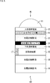
- the solid-state imaging device 30 includes an on-chip lens 11, an upper transparent electrode 12, a photoelectric conversion film (G) 13, a spectral correction buffer 31, a lower transparent electrode 14, an interlayer insulating layer 15, and photoelectrics in this order from the light incident surface side.
- the conversion layer (B) 18 and the photoelectric conversion layer (R) 19 are stacked.
- a through electrode 17 for transferring the charge converted by the photoelectric conversion film (G) 13 to a wiring layer (not shown) is formed.
- the solid-state imaging device 30 eliminates the spectral correction color filter 16 from the interlayer insulating film 15 of the solid-state imaging device 10 shown in FIG. 1, and instead, the photoelectric conversion film (G) 13 and the lower transparent electrode 14 The spectral correction buffer 31 is formed between them.
- the upper transparent electrode 12, the photoelectric conversion film (G) 13, the spectral correction buffer 31, and the lower transparent electrode 14 constitute a photoelectric conversion module.
- the material of the upper transparent electrode 12 and the lower transparent electrode 14 preferably has a band gap of at least 2.5 eV or more, preferably 3.1 eV or more, and is transparent to light in the visible region of 400 to 700 nm .
- ITO, IZO, IGZO, GZO and the like can be mentioned.
- a material having an absorption peak in a specific wavelength range is preferable.
- quantum dot materials low molecular weight organic materials, high molecular weight organic materials and the like can be mentioned.
- examples of quantum dot materials include ZnSe, CdSe, and the like.
- Examples of low molecular weight organic materials and high molecular weight organic materials include carbazole derivatives, amine derivatives, naphthalenediimide derivatives, phthalocyanine derivatives, thiophene derivatives, quinacridone derivatives, fullerene derivatives and the like.
- the thickness thereof can be thinner than that of the spectral correction color filter 16 of FIG.
- the spectral correction buffer 31 absorbs a wavelength range other than the wavelength range where the photoelectric conversion film (G) 13 performs photoelectric conversion to perform spectral correction, photoelectric conversion is not performed in the spectral correction buffer 31. Is desirable.
- FIG. 3 is an energy diagram showing requirements of carrier behavior in the spectral correction buffer 31. As shown in FIG.
- the spectral correction buffer 31 has a carrier extraction function from the photoelectric conversion film (G) 13 and a lower transparent electrode 14 in addition to the spectral correction function for restricting the passage of light in a specific wavelength range. And the electron injection block function to prevent the injection of electrons to the photoelectric conversion film (G) 13.
- the electron injection barrier which is the energy difference between the lowest unoccupied molecular orbital (LUMO) level of the spectral correction buffer 31 for realizing the electron injection block function and the lower transparent electrode 14 is at least 1.0 eV or more. If it is 5 eV or more, desirably 2.0 eV or more, the dark current can be sufficiently suppressed.
- the LUMO level of the buffer for spectral correction 31 is preferably around 3.0 eV because the work function is approximately 5 eV. Furthermore, when the bonding between the HOMO (Highest Occupied Molecular Orbital) level and the lower transparent electrode 14 is considered, the HOMO of the buffer 31 for spectral correction is required to have a HOMO level equal to or lower than that of the lower transparent electrode 14 Be
- FIG. 4 is a diagram showing a spectral correction function by the spectral correction buffer 31.
- the horizontal axis indicates the wavelength, and the vertical axis indicates the intensity.
- the curve B is the wavelength range of light incident on the photoelectric conversion layer (B) 18 and the curve G is the photoelectric conversion film (G) 13 with the spectral correction buffer 31 omitted from the solid-state imaging device 30.
- the wavelength range of incident light and the curve R indicate the wavelength range of light incident on the photoelectric conversion layer (R) 19.
- a curve L1 in FIG. B indicates a wavelength range in which the spectral correction buffer 31 absorbs (limits the passage).
- curve C shows the wavelength range of light incident on the photoelectric conversion layer (B) 18
- curve G shows the wavelength range of light incident on the photoelectric conversion film (G) 13
- curve R The wavelength range of the light which injects into photoelectric converting layer (R) 19 is shown.
- the curve B in FIG. A when the peak of the wavelength range of light incident on the photoelectric conversion layer (B) 18 spreads to the low wavelength side, the curve L1 in FIG. A spectral correction buffer 31 is used to absorb the low wavelength side of the blue light peak.
- the spectral shape of the light which injects into the photoelectric converting layer (B) 18 can be improved.
- the spectral correction buffer 31 is formed in the photoelectric conversion module, there is no need to form the spectral correction color filter 16 in the interlayer insulating film 15, so the interlayer insulating film 15 can be used. It can be thinned.
- the photoelectric conversion module including the spectral correction buffer 31 can be formed consistently, it is possible to reduce the overall man-hours.
- the margin regarding the heat resistance of the formation process of the lower transparent electrode 14, patterning, etc. can be improved.
- the height can be reduced compared to the solid-state imaging device 10, the light collection efficiency and the oblique light resistance can be improved.
- FIG. 5 is a cross-sectional view showing a second configuration example (second embodiment) of the solid-state imaging device to which the present disclosure is applied.
- the components common to the solid-state imaging device 40 according to the second embodiment and the solid-state imaging devices 10 and 30 described above are denoted by the same reference numerals, and the description thereof will be appropriately omitted.
- This solid-state imaging device 40 is obtained by adding a hole blocking layer 41 between the upper transparent electrode 12 and the photoelectric conversion film (G) 13 in addition to the solid-state imaging device 30 shown in FIG.
- the upper transparent electrode 12, the hole blocking layer 41, the photoelectric conversion film (G) 13, the spectral correction buffer 31, and the lower transparent electrode 14 constitute a photoelectric conversion module.
- the hole block layer 41 is not required to have a spectral correction function, NiO, ZnO or the like can be used as the inorganic oxide semiconductor in addition to the same material as the material of the spectral correction buffer 31 as the material.
- the hole blocking layer 41 may be formed using a single material, or may have a laminated structure using a plurality of materials.
- FIG. 6 is an energy diagram showing requirements of carrier behavior in the hole blocking layer 41 and the buffer 31 for spectral correction.
- the hole blocking layer 41 has a dark current suppression blocking function to prevent the injection of holes from the upper transparent electrode 12 to the photoelectric conversion film (G) 13.
- the HOMO level of the hole blocking layer 41 is at least 1 eV or more, preferably 1.5 eV or more, preferably 2.0 eV or more from the upper transparent electrode 12. Is preferred.
- the spectral correction buffer 31 is the same as that described above with reference to FIG.
- the solid-state imaging device 40 since the spectral correction buffer 31 and the hole block layer 41 are formed in the photoelectric conversion module, in addition to the same effect as the solid-state imaging device 30, the conversion in the photoelectric conversion film (G) 13 is performed. Efficiency can be further improved.
- FIG. 7 is a cross-sectional view showing a third configuration example (third embodiment) of the solid-state imaging device to which the present disclosure is applied.
- the components common to the solid-state imaging device 50 according to the third embodiment and the solid-state imaging devices 10, 30, and 40 described above are denoted by the same reference numerals, and the description thereof will be appropriately omitted. .
- the solid-state imaging device 50 is obtained by replacing the hole blocking layer 41 of the solid-state imaging device 40 shown in FIG. 5 with a spectral correction buffer 51.
- the upper transparent electrode 12, the spectral correction buffer 51, the photoelectric conversion film (G) 13, the spectral correction buffer 31, and the lower transparent electrode 14 constitute a photoelectric conversion module.
- the spectral correction buffer 51 can be formed of the same material as the spectral correction buffer 31.
- the spectral correction buffers 51 and 31 are formed in the photoelectric conversion module, the same effect as that of the solid-state imaging device 40 can be obtained.
- the spectral correction buffer 51 by providing the spectral correction buffer 51, the amount of light incident on the lower layer side of the spectral correction buffer 51 is somewhat reduced.
- FIG. 8 is a cross-sectional view showing a fourth configuration example (fourth embodiment) of the solid-state imaging device to which the present disclosure is applied.
- the components common to the solid-state imaging device 60 according to the fourth embodiment and the solid-state imaging devices 10, 30, 40, and 50 described above are denoted by the same reference numerals, and the description thereof will be appropriately made. I omit it.
- the solid-state imaging device 60 includes a photoelectric conversion film (B) for performing photoelectric conversion on light in the wavelength range of the on-chip lens 11, the upper transparent electrode 61, the spectral correction buffer 62, and B sequentially from the light incident surface side.
- a photoelectric conversion film (B) for performing photoelectric conversion on light in the wavelength range of the on-chip lens 11, the upper transparent electrode 61, the spectral correction buffer 62, and B sequentially from the light incident surface side.
- 63, lower transparent electrode 64, interlayer insulating layer 65, upper transparent electrode 66, photoelectric conversion film (G) 67 for performing photoelectric conversion on light in the wavelength range of G, buffer for spectral correction 68, lower transparent electrode 69, interlayer An insulating layer 70 and a photoelectric conversion layer (R) 71 that performs photoelectric conversion on light in a wavelength range of R are stacked.
- each of the photoelectric conversion film (B) 63 and the photoelectric conversion film (G) 67 through electrodes (not shown) for transferring the converted charge to the wiring layer are formed.
- the upper transparent electrode 61, the spectral correction buffer 62, the photoelectric conversion film (B) 63, and the lower transparent electrode 64 constitute a first photoelectric conversion module. Further, the upper transparent electrode 66, the photoelectric conversion film (G) 67, the spectral correction buffer 68, and the lower transparent electrode 69 constitute a second photoelectric conversion module.
- the materials of the upper transparent electrode 61 and the like and the lower transparent electrode 64 and the like are the same as those of the upper transparent electrode 12 and the lower transparent electrode 14 in the solid-state imaging device 30 described above.
- the materials of the spectral correction buffer 62 and the like are the same as the spectral correction buffer 31 in the solid-state imaging device 30 described above.
- FIG. 9 is a diagram showing a spectral correction function by the spectral correction buffers 62 and 68 in the solid-state imaging device 60, and the horizontal axis indicates the wavelength, and the vertical axis indicates the intensity.
- the curve B represents the wavelength range of light incident on the photoelectric conversion film (B) 63
- the curve G represents the photoelectric conversion film (G), with the spectral correction buffers 62 and 68 omitted from the solid-state imaging device 60.
- a wavelength range of light incident on 67 and a curve R indicate a wavelength range of light incident on the photoelectric conversion layer (R) 71.
- a curve L11 in FIG. B shows a wavelength range where the spectral correction buffer 62 absorbs (limits the passage).
- a curve L12 indicates a wavelength range where the spectral correction buffer 68 absorbs (passes).
- the curve B represents the wavelength range of light incident on the photoelectric conversion film (B) 63
- the curve G represents the wavelength range of light incident on the photoelectric conversion film (G) 67
- the curve R The wavelength range of the light which injects into the photoelectric converting layer (R) 71 is shown.
- the curve L11 in FIG. A spectral correction buffer 31 is used to absorb the low wavelength side of the blue light peak.
- the curve R in FIG. A when absorption leakage occurs at the cross point of the wavelength range of B and the wavelength range of G, the absorption as shown in the curve L12 of FIG. A spectral correction buffer 68 that leaks and absorbs light in the wavelength range is used.
- the peak of the wavelength of light incident on the photoelectric conversion film (B) 63 can be improved.
- color mixing in the photoelectric conversion layer (R) 71 can be reduced.
- the height can be reduced compared to the solid-state imaging device 10, and the light collection efficiency and the oblique light resistance can be improved.
- FIG. 10 is a cross-sectional view showing a fifth configuration example (fifth embodiment) of the solid-state imaging device to which the present disclosure is applied.
- the components common to the solid-state imaging device 80 according to the fifth embodiment and the solid-state imaging devices 10, 30, 40, 50, and 60 described above are denoted by the same reference numerals, and the description thereof Is omitted as appropriate.
- the solid-state imaging device 80 includes an on-chip lens 11, an upper transparent electrode 81, a photoelectric conversion film (R) 82 for performing photoelectric conversion on light in the wavelength range of R, and a buffer for spectral correction.
- each of the photoelectric conversion film (R) 82 and the photoelectric conversion film (G) 87 through electrodes (not shown) for transferring the converted charge to the wiring layer are formed.
- the upper transparent electrode 81, the photoelectric conversion film (R) 82, the spectral correction buffer 83, and the lower transparent electrode 84 constitute a first photoelectric conversion module. Further, the upper transparent electrode 86, the photoelectric conversion film (G) 87, the spectral correction buffer 88, and the lower transparent electrode 89 constitute a second photoelectric conversion module.
- Materials for the upper transparent electrode 81 and the like and the lower transparent electrode 84 and the like are the same as the upper transparent electrode 12 and the lower transparent electrode 14 in the solid-state imaging device 30 described above.
- the materials of the spectral correction buffer 83 and the like are the same as the spectral correction buffer 31 in the solid-state imaging device 30 described above.
- FIG. 11 is a diagram showing a spectral correction function by the spectral correction buffers 83 and 88 in the solid-state imaging device 80, and the horizontal axis indicates the wavelength, and the vertical axis indicates the intensity.
- the curve B represents the wavelength range of light incident on the photoelectric conversion layer (B) 91
- the curve G represents the photoelectric conversion film (G), with the spectral correction buffers 83 and 88 omitted from the solid-state imaging device 80.
- a wavelength range of light incident on 87 and a curve R indicate a wavelength range of light incident on the photoelectric conversion film (R) 82.
- a curve L21 in FIG. B indicates a wavelength range where the spectral correction buffer 83 absorbs (limits the passage).
- a curve L22 indicates a wavelength range in which the spectral correction buffer 88 absorbs (passes).
- the curve B is the wavelength range of light incident on the photoelectric conversion layer (B) 91
- the curve G is the wavelength range of light incident on the photoelectric conversion film (G) 87
- the curve R is The wavelength range of the light which injects into the photoelectric conversion film (R) 82 is shown.
- a spectral correction buffer 88 that absorbs the low wavelength side of the blue light peak as shown by curve L22 in FIG. A buffer for spectral correction 83 is used which causes absorption leakage and absorbs light in the wavelength range.
- the peak of the wavelength of light incident on the photoelectric conversion layer (B) 91 can be improved, and color mixing in the photoelectric conversion layer (B) 91 can be reduced.
- the height can be reduced compared to the solid-state imaging device 10, and the light collection efficiency and the oblique light resistance can be improved.
- FIG. 12 is a view showing a use example using the solid-state imaging device 30 to 80 described above.
- the solid-state imaging devices 30 to 80 described above can be used, for example, in various cases for sensing light such as visible light, infrared light, ultraviolet light, and X-rays as described below.
- a device that captures images for viewing such as a digital camera or a portable device with a camera function-For safe driving such as automatic stop, recognition of driver's condition, etc.
- a device provided for traffic such as an on-vehicle sensor for capturing images of the rear, surroundings, inside of a car, a monitoring camera for monitoring a traveling vehicle or a road, a distance measuring sensor for measuring distance between vehicles, etc.
- Devices used for home appliances such as TVs, refrigerators, air conditioners, etc. to perform imaging and device operation according to the gesture ⁇ Endoscopes, devices for performing blood vessel imaging by receiving infrared light, etc.
- Equipment provided for medical and healthcare use-Equipment provided for security such as surveillance cameras for crime prevention, cameras for personal identification, etc.
- -Skin measuring equipment for photographing skin, photographing for scalp For beauty such as microscope to do Equipment provided for sports Equipment used for sports, such as action cameras and wearable cameras for sports applications, etc.
- Equipment provided for agriculture such as cameras for monitoring the condition of fields and crops
- the present disclosure can also be configured as follows. (1) In a vertical spectroscopy solid-state imaging device in which a plurality of photoelectric conversion units are stacked in the area of each pixel, A first photoelectric conversion unit that performs photoelectric conversion on light in a first wavelength range of incident light, a first upper electrode and a first lower electrode formed with the first photoelectric conversion unit interposed therebetween And a first photoelectric conversion module having a first spectral correction unit formed by being stacked in the first photoelectric conversion unit between the first upper electrode and the first lower electrode. A second photoelectric conversion unit configured to perform photoelectric conversion on light of a second wavelength range different from the first wavelength range of light having passed through the first photoelectric conversion module.
- the solid-state imaging device further including a conversion unit.
- the first spectral correction unit has at least one of a carrier extraction function for the first photoelectric conversion unit, and an electron injection block function for the first photoelectric conversion unit, according to (1) or (2).
- the first spectral correction unit is formed of a quantum dot material having a light absorption peak in a specific wavelength range, a low molecular weight organic material, or a high molecular weight organic material according to any one of (1) to (3).
- the first photoelectric conversion module In the first photoelectric conversion module, the first upper electrode, the first photoelectric conversion unit, the first spectral correction unit, and the first lower electrode are stacked in order from the light incident side.
- the solid-state imaging device according to any one of (1) to (4).
- the first photoelectric conversion module further includes a hole blocking portion, and the first upper electrode, the hole blocking portion, the first photoelectric conversion portion, and the first photoelectric conversion portion are arranged in order from the light incident side.
- the solid-state imaging device according to any one of (1) to (5), wherein a spectral correction unit and the first lower electrode are stacked.
- the first photoelectric conversion module further includes a second spectral correction unit, and the first upper electrode, the second spectral correction unit, and the first photoelectric conversion unit in order from the light incident side.
- the solid-state imaging device according to any one of (1) to (5), wherein the first spectral correction unit and the first lower electrode are stacked.
- (1), (3) to (7) The solid-state imaging device according to any one of the above.
- the solid-state imaging device is A first photoelectric conversion unit that performs photoelectric conversion on light in a first wavelength range of incident light, a first upper electrode and a first lower electrode formed with the first photoelectric conversion unit interposed therebetween And a first photoelectric conversion module having a first spectral correction unit formed by being stacked in the first photoelectric conversion unit between the first upper electrode and the first lower electrode.
- An electronic apparatus comprising: a second photoelectric conversion unit that performs photoelectric conversion on light in a second wavelength range different from the first wavelength range of light having passed through the first photoelectric conversion module.
Landscapes
- Engineering & Computer Science (AREA)
- Multimedia (AREA)
- Signal Processing (AREA)
- Solid State Image Pick-Up Elements (AREA)
Abstract
La présente invention concerne un élément d'imagerie à semi-conducteurs et un appareil électronique de telle sorte qu'une chute de l'efficacité de collecte de lumière et une détérioration de la résistance à la lumière oblique peuvent être réduites au minimum, et une réduction du profil de l'élément d'imagerie à semi-conducteurs peut être obtenue. Selon un premier aspect de la présente invention, l'élément d'imagerie à semi-conducteurs est un élément d'imagerie à semi-conducteurs du type à séparation spectrale verticale dans lequel une pluralité de parties de conversion photoélectrique sont stratifiées dans chaque région de pixel. L'élément d'imagerie à semi-conducteurs comprend : un premier module de conversion photoélectrique ayant une première partie de conversion photoélectrique pour effectuer une conversion photoélectrique d'un faisceau lumineux dans une première région de longueur d'onde du faisceau lumineux entrant, une première électrode supérieure et une première électrode inférieure formées de manière à prendre en sandwich la première partie de conversion photoélectrique entre elles, et une première partie de correction spectrale formée en étant stratifiée sur la première unité de conversion photoélectrique entre la première électrode supérieure et la première électrode inférieure ; et une seconde partie de conversion photoélectrique réalisant une conversion photoélectrique d'un faisceau lumineux dans une seconde région de longueur d'onde différente de la première région de longueur d'onde du faisceau lumineux qui a traversé le premier module de conversion photoélectrique. La présente invention peut s'appliquer, par exemple, à un capteur d'image CMOS.
Priority Applications (2)
| Application Number | Priority Date | Filing Date | Title |
|---|---|---|---|
| US16/086,248 US11211422B2 (en) | 2016-03-28 | 2017-03-14 | Solid-state image sensor and electronic apparatus |
| US17/539,552 US20220165781A1 (en) | 2016-03-28 | 2021-12-01 | Solid-state image sensor and electronic apparatus |
Applications Claiming Priority (2)
| Application Number | Priority Date | Filing Date | Title |
|---|---|---|---|
| JP2016064074 | 2016-03-28 | ||
| JP2016-064074 | 2016-03-28 |
Related Child Applications (2)
| Application Number | Title | Priority Date | Filing Date |
|---|---|---|---|
| US16/086,248 A-371-Of-International US11211422B2 (en) | 2016-03-28 | 2017-03-14 | Solid-state image sensor and electronic apparatus |
| US17/539,552 Continuation US20220165781A1 (en) | 2016-03-28 | 2021-12-01 | Solid-state image sensor and electronic apparatus |
Publications (1)
| Publication Number | Publication Date |
|---|---|
| WO2017169719A1 true WO2017169719A1 (fr) | 2017-10-05 |
Family
ID=59964322
Family Applications (1)
| Application Number | Title | Priority Date | Filing Date |
|---|---|---|---|
| PCT/JP2017/010103 Ceased WO2017169719A1 (fr) | 2016-03-28 | 2017-03-14 | Élément d'imagerie à semi-conducteurs et appareil électronique |
Country Status (2)
| Country | Link |
|---|---|
| US (2) | US11211422B2 (fr) |
| WO (1) | WO2017169719A1 (fr) |
Cited By (1)
| Publication number | Priority date | Publication date | Assignee | Title |
|---|---|---|---|---|
| WO2020080072A1 (fr) * | 2018-10-17 | 2020-04-23 | パナソニックIpマネジメント株式会社 | Élément de conversion photoélectrique et capteur d'image |
Families Citing this family (2)
| Publication number | Priority date | Publication date | Assignee | Title |
|---|---|---|---|---|
| WO2017169719A1 (fr) * | 2016-03-28 | 2017-10-05 | ソニー株式会社 | Élément d'imagerie à semi-conducteurs et appareil électronique |
| WO2019049946A1 (fr) * | 2017-09-11 | 2019-03-14 | 富士フイルム株式会社 | Élément de conversion photoélectrique, photodétecteur, élément d'imagerie et composé |
Citations (2)
| Publication number | Priority date | Publication date | Assignee | Title |
|---|---|---|---|---|
| WO2015178116A1 (fr) * | 2014-05-23 | 2015-11-26 | ソニー株式会社 | Élément de conversion photoélectrique, dispositif d'imagerie à semi-conducteur, matière organique photo-absorbante, et intermédiaire de matière organique photo-absorbante |
| WO2016027675A1 (fr) * | 2014-08-20 | 2016-02-25 | 東レ株式会社 | Élément de conversion photoélectrique, et capteur d'image, cellule solaire, capteur de détection monochrome et capteur souple utilisant chacun ledit élément de conversion photoélectrique |
Family Cites Families (7)
| Publication number | Priority date | Publication date | Assignee | Title |
|---|---|---|---|---|
| JP4825542B2 (ja) * | 2006-02-23 | 2011-11-30 | 富士フイルム株式会社 | 固体撮像素子の製造方法 |
| JP2007287930A (ja) | 2006-04-17 | 2007-11-01 | Fujifilm Corp | 固体撮像素子 |
| KR101327793B1 (ko) * | 2007-10-08 | 2013-11-11 | 삼성전자주식회사 | 티오펜 유도체를 이용한 시모스 이미지 센서 |
| JP2009182095A (ja) * | 2008-01-30 | 2009-08-13 | Fujifilm Corp | 光電変換素子及び固体撮像素子 |
| JP2009260160A (ja) * | 2008-04-21 | 2009-11-05 | Panasonic Corp | 光半導体装置 |
| KR102261855B1 (ko) * | 2014-06-13 | 2021-06-07 | 삼성전자주식회사 | 색분리 소자를 포함하는 적층형 이미지 센서 및 상기 이미지 센서를 포함하는 촬상 장치 |
| WO2017169719A1 (fr) * | 2016-03-28 | 2017-10-05 | ソニー株式会社 | Élément d'imagerie à semi-conducteurs et appareil électronique |
-
2017
- 2017-03-14 WO PCT/JP2017/010103 patent/WO2017169719A1/fr not_active Ceased
- 2017-03-14 US US16/086,248 patent/US11211422B2/en not_active Expired - Fee Related
-
2021
- 2021-12-01 US US17/539,552 patent/US20220165781A1/en active Pending
Patent Citations (2)
| Publication number | Priority date | Publication date | Assignee | Title |
|---|---|---|---|---|
| WO2015178116A1 (fr) * | 2014-05-23 | 2015-11-26 | ソニー株式会社 | Élément de conversion photoélectrique, dispositif d'imagerie à semi-conducteur, matière organique photo-absorbante, et intermédiaire de matière organique photo-absorbante |
| WO2016027675A1 (fr) * | 2014-08-20 | 2016-02-25 | 東レ株式会社 | Élément de conversion photoélectrique, et capteur d'image, cellule solaire, capteur de détection monochrome et capteur souple utilisant chacun ledit élément de conversion photoélectrique |
Cited By (4)
| Publication number | Priority date | Publication date | Assignee | Title |
|---|---|---|---|---|
| WO2020080072A1 (fr) * | 2018-10-17 | 2020-04-23 | パナソニックIpマネジメント株式会社 | Élément de conversion photoélectrique et capteur d'image |
| JPWO2020080072A1 (ja) * | 2018-10-17 | 2021-09-16 | パナソニックIpマネジメント株式会社 | 光電変換素子およびイメージセンサ |
| JP7365611B2 (ja) | 2018-10-17 | 2023-10-20 | パナソニックIpマネジメント株式会社 | 光電変換素子およびイメージセンサ |
| US11812625B2 (en) | 2018-10-17 | 2023-11-07 | Panasonic Intellectual Property Management Co., Ltd. | Photoelectric converter and image sensor |
Also Published As
| Publication number | Publication date |
|---|---|
| US20220165781A1 (en) | 2022-05-26 |
| US11211422B2 (en) | 2021-12-28 |
| US20200295074A1 (en) | 2020-09-17 |
Similar Documents
| Publication | Publication Date | Title |
|---|---|---|
| KR102651629B1 (ko) | 광전변환 소자 및 고체 촬상 장치 | |
| WO2020255999A1 (fr) | Élément de conversion photoélectrique, dispositif de détection de lumière, système de détection de lumière, appareil électronique et corps mobile | |
| US11190711B2 (en) | Solid-state image sensor and electronic device | |
| US12218167B2 (en) | Solid-state imaging device and electronic device | |
| JP7676486B2 (ja) | 光電変換素子および固体撮像装置 | |
| US20220165781A1 (en) | Solid-state image sensor and electronic apparatus | |
| WO2022163296A1 (fr) | Dispositif d'imagerie | |
| CN114631199B (zh) | 光电转换元件和摄像装置 | |
| US20230276641A1 (en) | Photoelectric conversion element and imaging device | |
| KR102828792B1 (ko) | 고체 촬상 장치 및 전자 기기 | |
| US12376446B2 (en) | Photoelectric conversion element and imaging device | |
| WO2022131101A1 (fr) | Élément de conversion photoélectrique, dispositif de détection de lumière, système de détection de lumière, équipement électronique et corps mobile | |
| US20230207598A1 (en) | Photoelectric converter and imaging device | |
| CN117157763A (zh) | 光检测装置、光检测系统、电子设备和移动体 | |
| TWI918716B (zh) | 固態攝像裝置及電子機器 | |
| WO2023223801A1 (fr) | Élément de conversion photoélectrique, dispositif photodétecteur et appareil électronique | |
| KR20260049625A (ko) | 광 검출 장치 | |
| WO2026074912A1 (fr) | Dispositif de détection de lumière et équipement électronique | |
| WO2025203182A1 (fr) | Dispositif de détection de lumière | |
| WO2025121007A1 (fr) | Dispositif de détection de lumière | |
| WO2023085188A1 (fr) | Film semi-conducteur organique, élément de conversion photoélectrique et dispositif d'imagerie | |
| WO2022107654A1 (fr) | Élément de conversion photoélectrique et dispositif d'imagerie à semi-conducteurs |
Legal Events
| Date | Code | Title | Description |
|---|---|---|---|
| NENP | Non-entry into the national phase |
Ref country code: DE |
|
| 121 | Ep: the epo has been informed by wipo that ep was designated in this application |
Ref document number: 17774263 Country of ref document: EP Kind code of ref document: A1 |
|
| 122 | Ep: pct application non-entry in european phase |
Ref document number: 17774263 Country of ref document: EP Kind code of ref document: A1 |
|
| NENP | Non-entry into the national phase |
Ref country code: JP |