WO2017169961A1 - Dispositif d'affichage et dispositif électronique - Google Patents
Dispositif d'affichage et dispositif électronique Download PDFInfo
- Publication number
- WO2017169961A1 WO2017169961A1 PCT/JP2017/011144 JP2017011144W WO2017169961A1 WO 2017169961 A1 WO2017169961 A1 WO 2017169961A1 JP 2017011144 W JP2017011144 W JP 2017011144W WO 2017169961 A1 WO2017169961 A1 WO 2017169961A1
- Authority
- WO
- WIPO (PCT)
- Prior art keywords
- electrode
- display device
- light emitting
- display
- layer
- Prior art date
- Legal status (The legal status is an assumption and is not a legal conclusion. Google has not performed a legal analysis and makes no representation as to the accuracy of the status listed.)
- Ceased
Links
Images












Classifications
-
- H—ELECTRICITY
- H10—SEMICONDUCTOR DEVICES; ELECTRIC SOLID-STATE DEVICES NOT OTHERWISE PROVIDED FOR
- H10K—ORGANIC ELECTRIC SOLID-STATE DEVICES
- H10K59/00—Integrated devices, or assemblies of multiple devices, comprising at least one organic light-emitting element covered by group H10K50/00
- H10K59/80—Constructional details
- H10K59/875—Arrangements for extracting light from the devices
- H10K59/878—Arrangements for extracting light from the devices comprising reflective means
-
- G—PHYSICS
- G09—EDUCATION; CRYPTOGRAPHY; DISPLAY; ADVERTISING; SEALS
- G09F—DISPLAYING; ADVERTISING; SIGNS; LABELS OR NAME-PLATES; SEALS
- G09F9/00—Indicating arrangements for variable information in which the information is built-up on a support by selection or combination of individual elements
- G09F9/30—Indicating arrangements for variable information in which the information is built-up on a support by selection or combination of individual elements in which the desired character or characters are formed by combining individual elements
- G09F9/301—Indicating arrangements for variable information in which the information is built-up on a support by selection or combination of individual elements in which the desired character or characters are formed by combining individual elements flexible foldable or roll-able electronic displays, e.g. thin LCD, OLED
-
- H—ELECTRICITY
- H05—ELECTRIC TECHNIQUES NOT OTHERWISE PROVIDED FOR
- H05B—ELECTRIC HEATING; ELECTRIC LIGHT SOURCES NOT OTHERWISE PROVIDED FOR; CIRCUIT ARRANGEMENTS FOR ELECTRIC LIGHT SOURCES, IN GENERAL
- H05B33/00—Electroluminescent light sources
- H05B33/12—Light sources with substantially two-dimensional [2D] radiating surfaces
- H05B33/26—Light sources with substantially two-dimensional [2D] radiating surfaces characterised by the composition or arrangement of the conductive material used as an electrode
-
- H—ELECTRICITY
- H10—SEMICONDUCTOR DEVICES; ELECTRIC SOLID-STATE DEVICES NOT OTHERWISE PROVIDED FOR
- H10K—ORGANIC ELECTRIC SOLID-STATE DEVICES
- H10K50/00—Organic light-emitting devices
- H10K50/10—OLEDs or polymer light-emitting diodes [PLED]
- H10K50/11—OLEDs or polymer light-emitting diodes [PLED] characterised by the electroluminescent [EL] layers
-
- H—ELECTRICITY
- H10—SEMICONDUCTOR DEVICES; ELECTRIC SOLID-STATE DEVICES NOT OTHERWISE PROVIDED FOR
- H10K—ORGANIC ELECTRIC SOLID-STATE DEVICES
- H10K50/00—Organic light-emitting devices
- H10K50/10—OLEDs or polymer light-emitting diodes [PLED]
- H10K50/14—Carrier transporting layers
- H10K50/15—Hole transporting layers
-
- H—ELECTRICITY
- H10—SEMICONDUCTOR DEVICES; ELECTRIC SOLID-STATE DEVICES NOT OTHERWISE PROVIDED FOR
- H10K—ORGANIC ELECTRIC SOLID-STATE DEVICES
- H10K50/00—Organic light-emitting devices
- H10K50/80—Constructional details
- H10K50/85—Arrangements for extracting light from the devices
-
- H—ELECTRICITY
- H10—SEMICONDUCTOR DEVICES; ELECTRIC SOLID-STATE DEVICES NOT OTHERWISE PROVIDED FOR
- H10K—ORGANIC ELECTRIC SOLID-STATE DEVICES
- H10K50/00—Organic light-emitting devices
- H10K50/80—Constructional details
- H10K50/85—Arrangements for extracting light from the devices
- H10K50/856—Arrangements for extracting light from the devices comprising reflective means
-
- H—ELECTRICITY
- H10—SEMICONDUCTOR DEVICES; ELECTRIC SOLID-STATE DEVICES NOT OTHERWISE PROVIDED FOR
- H10K—ORGANIC ELECTRIC SOLID-STATE DEVICES
- H10K50/00—Organic light-emitting devices
- H10K50/80—Constructional details
- H10K50/85—Arrangements for extracting light from the devices
- H10K50/858—Arrangements for extracting light from the devices comprising refractive means, e.g. lenses
-
- H—ELECTRICITY
- H10—SEMICONDUCTOR DEVICES; ELECTRIC SOLID-STATE DEVICES NOT OTHERWISE PROVIDED FOR
- H10K—ORGANIC ELECTRIC SOLID-STATE DEVICES
- H10K59/00—Integrated devices, or assemblies of multiple devices, comprising at least one organic light-emitting element covered by group H10K50/00
-
- H—ELECTRICITY
- H10—SEMICONDUCTOR DEVICES; ELECTRIC SOLID-STATE DEVICES NOT OTHERWISE PROVIDED FOR
- H10K—ORGANIC ELECTRIC SOLID-STATE DEVICES
- H10K59/00—Integrated devices, or assemblies of multiple devices, comprising at least one organic light-emitting element covered by group H10K50/00
- H10K59/80—Constructional details
- H10K59/875—Arrangements for extracting light from the devices
- H10K59/879—Arrangements for extracting light from the devices comprising refractive means, e.g. lenses
-
- H—ELECTRICITY
- H10—SEMICONDUCTOR DEVICES; ELECTRIC SOLID-STATE DEVICES NOT OTHERWISE PROVIDED FOR
- H10K—ORGANIC ELECTRIC SOLID-STATE DEVICES
- H10K77/00—Constructional details of devices covered by this subclass and not covered by groups H10K10/80, H10K30/80, H10K50/80 or H10K59/80
- H10K77/10—Substrates, e.g. flexible substrates
-
- H—ELECTRICITY
- H10—SEMICONDUCTOR DEVICES; ELECTRIC SOLID-STATE DEVICES NOT OTHERWISE PROVIDED FOR
- H10K—ORGANIC ELECTRIC SOLID-STATE DEVICES
- H10K59/00—Integrated devices, or assemblies of multiple devices, comprising at least one organic light-emitting element covered by group H10K50/00
- H10K59/30—Devices specially adapted for multicolour light emission
- H10K59/38—Devices specially adapted for multicolour light emission comprising colour filters or colour changing media [CCM]
-
- Y—GENERAL TAGGING OF NEW TECHNOLOGICAL DEVELOPMENTS; GENERAL TAGGING OF CROSS-SECTIONAL TECHNOLOGIES SPANNING OVER SEVERAL SECTIONS OF THE IPC; TECHNICAL SUBJECTS COVERED BY FORMER USPC CROSS-REFERENCE ART COLLECTIONS [XRACs] AND DIGESTS
- Y02—TECHNOLOGIES OR APPLICATIONS FOR MITIGATION OR ADAPTATION AGAINST CLIMATE CHANGE
- Y02E—REDUCTION OF GREENHOUSE GAS [GHG] EMISSIONS, RELATED TO ENERGY GENERATION, TRANSMISSION OR DISTRIBUTION
- Y02E10/00—Energy generation through renewable energy sources
- Y02E10/50—Photovoltaic [PV] energy
- Y02E10/549—Organic PV cells
Definitions
- This disclosure relates to a display device and an electronic device.
- Patent Document 1 discloses a display device including a light-emitting element including a first electrode, a light-emitting layer, and a second electrode that are stacked so that the surface has an uneven pattern.
- a display device including a light-emitting element including a first electrode, a light-emitting layer, and a second electrode that are stacked so that the surface has an uneven pattern.
- the reflected light is reflected between the first electrode and the second electrode. It is described that since the resonance hardly occurs even when it is repeated, the viewing angle characteristics of the display device can be improved.
- Patent Document 2 discloses a display device including a light emitting element including a first electrode, a light emitting layer, and a second electrode stacked so as to have a convex curved shape.
- Japanese Patent Application Laid-Open No. H10-260260 describes that the light emitting surface of the light emitting element can be formed into a convex shape with this configuration, and thus the viewing angle characteristics of the display device can be improved.
- Patent Document 3 discloses a display device including a light emitting element in which a first electrode, a light emitting layer, and a second electrode are stacked on an uneven structure formed on a substrate surface.
- the area of the light emitting part including the light emitting layer can be made larger than the area of the opening for taking out light from the light emitting part, so that the light extraction efficiency can be improved. Is described.
- a display device having a relatively small display surface such as a head mounted display (HMD) or an electronic viewfinder (EVF) of a digital camera
- HMD head mounted display
- EVF electronic viewfinder
- electronic devices are also equipped with small display devices.
- light rays from the display surface of the display device can be imaged on the user's eyeball through an optical system such as a lens, a mirror, and a diffraction grating, but further weight reduction of the electronic device, Due to the demand for miniaturization, the optical system tends to shrink. When the optical system is reduced, it is necessary to appropriately form a light beam on the user's eyeball with an optical system with a simpler configuration.
- the viewing angle characteristics of the display device can be improved by devising the configuration of the optical system. It is difficult to compensate, and the viewing angle characteristic of the display device directly leads to display quality visually recognized by the user. Therefore, the display device is required to further improve the viewing angle characteristics depending on the application.
- the present disclosure proposes a new and improved display device that can further improve the viewing angle characteristics, and an electronic device equipped with the display device.
- the light emitting unit includes a plurality of light emitting units formed on a substrate, and the light emitting unit has a light emitting layer in a stacking direction on a first electrode that functions as a reflective electrode and a second electrode.
- the surface facing the light emitting layer of the first electrode is inclined from a plane perpendicular to the stacking direction in at least a partial region in the display surface, and the inclination of the first electrode
- a display device is provided in which the direction has a distribution in the display surface.
- a display device that performs display based on an image signal
- the display device includes a plurality of light emitting units formed on a substrate, and the light emitting unit emits light
- the layer has a configuration sandwiched between the first electrode functioning as a reflective electrode and the second electrode in the stacking direction, and faces the light emitting layer of the first electrode at least in a partial region within the display surface.
- An electronic apparatus is provided in which a surface to be inclined is inclined from a surface perpendicular to the stacking direction, and the inclination direction of the first electrode has a distribution in a display surface.
- a surface facing the light emitting layer of the first electrode functioning as a reflective electrode is perpendicular to the stacking direction. Inclined with respect to the surface. Thereby, it becomes possible to control the main emission direction of light for each light emitting portion, that is, for each pixel.
- the inclination of the surface of the first electrode facing the light emitting layer has a distribution in the display surface. Therefore, for example, by adjusting the viewing angle characteristics of each pixel according to the application of the display device, it is possible to realize a desired viewing angle characteristic for the entire display surface.
- the viewing angle characteristics can be further improved.
- the above effects are not necessarily limited, and any of the effects shown in the present specification, or other effects that can be grasped from the present specification, together with the above effects or instead of the above effects. May be played.
- FIG. 5 is a diagram illustrating a configuration in the vicinity of a first electrode of the display device illustrated in FIG. 4. It is a figure for demonstrating the process flow at the time of forming the 1st electrode inclined from the horizontal surface shown in FIG. It is a figure for demonstrating the process flow at the time of forming the 1st electrode inclined from the horizontal surface shown in FIG. It is a figure for demonstrating the process flow at the time of forming the 1st electrode inclined from the horizontal surface shown in FIG. It is a figure for demonstrating the process flow at the time of forming the 1st electrode inclined from the horizontal surface shown in FIG.
- FIG. 1 It is sectional drawing which shows one structural example of the display apparatus which concerns on 3rd Embodiment. It is a figure for demonstrating the example of the other setting method of the area
- First embodiment 2-1 Overall configuration of display device 2-2. Details of structure of first electrode 2-3. 2. Manufacturing method Second embodiment 3-1. Overall configuration of display device 3-2. Manufacturing method 4. Third embodiment 4-1. 4. Overall configuration of display device Modified example 5-1. Modified example of distribution of tilt direction from first surface of first electrode in display surface 5-2. 5. Variation of tilt angle and tilt direction distribution of first electrode from horizontal plane in display surface and method for forming first electrode 6. Specific configuration example of display device Application example 8. Supplement
- a small display device can be mounted on an electronic device in applications such as HMD and EVF of a digital camera.
- an electronic device In such an electronic device, light rays from the display surface of the display device are imaged on the user's eyeball through an optical system such as a lens, a mirror, and a diffraction grating.
- an optical system such as a lens, a mirror, and a diffraction grating.
- FIG. 1 is a diagram schematically illustrating a locus of light rays from a small display device in an electronic device to a user's eyeball when the optical system is reduced.
- FIG. 1 in order to reduce the weight and size of an electronic device, it is necessary to reduce the optical system 205 and to further reduce the distance between the optical system 205 and the display device 1.
- the optical system 205 cannot be complicated, it is difficult to supplement the viewing angle characteristics of the display device 1 by devising the configuration of the optical system 205.
- a light beam having a wider angle that is, a light beam having a wider viewing angle
- the display device 1, particularly the display is provided in order to provide a high-quality display to the user.
- a light beam having a desired characteristic can be emitted even at a wider viewing angle, that is, having a better wide viewing angle characteristic.
- a display device in which a pixel is formed by providing a color filter (CF) in the upper layer of a white light emitting element and color display is performed by performing color conversion using the CF for each pixel.
- CF color filter
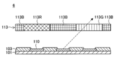
- FIG. 2 is a diagram schematically showing a cross-sectional configuration of a general display device.
- the general display device 6 includes a plurality of light emitting elements 110 arranged on the first substrate 101 at predetermined intervals, and a CF layer 113 provided above the light emitting elements 110. Is done.
- the CF layer 113 is configured such that red CF113R, green CF113G, and blue CF113B each having a predetermined area are continuously distributed in a horizontal plane.
- CF113a when it is not necessary to distinguish between CF113R, CF113G, and CF113B, one or more of them are simply referred to as CF113a.
- One pixel can be formed by a combination of one light emitting element 110 and one CF 113a.
- a pixel definition film 103 for defining pixels is provided between the light emitting elements 110 (that is, between pixels).
- the emitted light from a certain light emitting element 110 is schematically shown by an arrow.
- the emitted light from the light emitting element 110 does not enter the CF 113 ⁇ / b> B located immediately above the light emitting element 110, and the adjacent pixels The light enters the CF 113G, that is, color mixing occurs.
- the display device is a display device using an organic light emitting diode (OLED: Organic Light-Emitting Diode) (that is, an organic EL display (OELD: Organic Electro-Luminescence Display))
- OLED Organic Light-Emitting Diode
- OELD Organic Electro-Luminescence Display
- Attempts to reduce the thickness of the electrode layer, the protective layer, and the CF adhesive layer may greatly reduce the light emitting characteristics and protective properties of the OLED.
- reducing the area of the light emitting surface of the light emitting element leads to a reduction in the aperture ratio, so that the luminance may be greatly reduced.
- FIG. 3 is a diagram schematically illustrating the locus of light rays from the small display device 1 to the user's eyeball 203 without using an optical system in the electronic apparatus.
- the display surface 201 of the display device 1 and the eyeball 203 close to each other as shown in FIG.
- each pixel in the vicinity of the outer periphery of the display surface 201 is required to emit a light beam having a desired characteristic in a direction toward the center, contrary to the case shown in FIG.
- a light beam having a desired characteristic is emitted to each pixel in the vicinity of the center of the display surface 201 of the display device 1 in a direction substantially toward the front.
- a small display device 1 mounted on an electronic device has different viewing angle characteristics required for each pixel of the display device 1 depending on the optical design of the electronic device. Also, the viewing angle characteristics required for each pixel differ depending on the position in the display surface 201.
- the present inventors suppress the occurrence of color mixing in a display device and achieve a desired viewing angle for each pixel without causing other characteristics such as a decrease in luminance as described above.
- the present disclosure has been conceived.
- preferred embodiments of the present disclosure which have been conceived by the present inventors, will be described in detail.
- an embodiment in which the display device is an organic EL display will be described as an example of the present disclosure.
- the present disclosure is not limited to such an example, and the display device that is the subject of the present disclosure is a display device in which a light emitting portion is configured by sandwiching a light emitting layer between two electrodes, such as an inorganic EL display or a plasma display. If it exists, various display devices may be used.
- the light emitting portion is a portion that emits light toward the outside in each pixel of the display device.
- the light emitting unit corresponds to a light emitting element.
- the light emitting unit corresponds to a region corresponding to one discharge cell in the plasma display panel.
- FIG. 4 is a cross-sectional view illustrating a configuration example of the display device according to the first embodiment.
- FIG. 4 is a schematic partial cross-sectional view of the display device according to the first embodiment.
- FIGS. 4, 6, 7, 11, and 14 are schematically illustrated by simplifying the actual configuration.
- the display device 1 includes a first substrate 101, a plurality of light emitting elements 110 that emit white light including OLEDs formed on the first substrate 101, and the light emitting elements 110.
- the upper layer mainly includes a CF layer 113 in which CF of each color is formed corresponding to each of the light emitting elements 110.
- a second substrate 117 made of a material transparent to light from the light emitting element 110 is disposed on the CF layer 113.
- the first substrate 101 is provided with a thin film transistor (TFT) for driving the light emitting element 110 corresponding to each of the light emitting elements 110.
- TFT thin film transistor
- An arbitrary light emitting element 110 is selectively driven by the TFT. The light from the driven light emitting element 110 passes through the corresponding CF, and its color is appropriately converted, and is emitted from above through the second substrate 117, thereby displaying a desired image, characters, and the like. .
- the stacking direction of the layers in the display device 1 is also referred to as the vertical direction.
- the direction in which the first substrate 101 is disposed is defined as a downward direction
- the direction in which the second substrate 117 is disposed is defined as an upward direction.
- a surface perpendicular to the vertical direction is also referred to as a horizontal plane.
- the display device 1 shown in FIG. 1 is a top emission type display device that can be displayed in color and is driven by an active matrix method.
- the first embodiment is not limited to such an example, and the display device according to the first embodiment may be a display device driven by another method such as a passive matrix method, or the first substrate 101. It may be a bottom emission type display device in which light is emitted through the panel.
- the display device 1 can be mounted on various electronic devices having a display function. Specifically, for example, the display device 1 is incorporated in a television device, an electronic book, a smartphone, a personal digital assistant (PDA), a notebook PC (Personal Computer), a video camera, a game device, or the like. It can be used as a monitor device. Alternatively, the display device 1 can be applied to an EVF of a digital camera, an HMD, or the like.
- the display device 1 is configured by laminating a light emitting element 110, a protective film 111, and a CF layer 113 in this order on a first substrate 101.
- the display device 1 is a so-called on-chip color filter (OCCF) type display device in which the CF layer 113 is formed on the first substrate 101 on which the light emitting element 110 is formed.
- the display device 1 is manufactured by bonding the second substrate 117 to the uppermost CF layer 113 through the sealing resin film 115.
- the light emitting device 110 includes a plurality of first electrodes 105 (anodes 105) arranged on the first substrate 101 in a predetermined pattern and electrically insulated from each other, and an organic layer formed on the first electrode 105. 107 and a second electrode 109 (cathode 109) formed on the organic layer 107. A stacked structure of the first electrode 105, the organic layer 107, and the second electrode 109 corresponding to the pattern of one first electrode 105 corresponds to one light emitting element 110.
- the organic layer 107 includes a light emitting layer made of an organic light emitting material and is configured to emit white light.
- the first electrode 105 is formed of a material that can reflect light from the organic layer 107. That is, the first electrode 105 functions as a reflection electrode as well as an anode.
- the second electrode 109 is formed of a material that can transmit light from the organic layer 107.
- a pixel definition film 103 that defines a pixel region is formed between the patterns of the adjacent first electrodes 105, that is, between the light emitting elements 110.
- the pixel defining film 103 is formed to have an opening that exposes the first electrode 105 at a portion corresponding to the first electrode 105.
- the surface exposed at the opening of the first electrode 105 corresponds to the light emitting surface of the light emitting element 110.
- the emitted light from the organic layer 107 is reflected directly or on the surface of the first electrode 105, and the second electrode 109, the protective film 111, the CF layer 113, the sealing resin film 115, and the second substrate 117 are arranged in this order. It passes and exits towards the outside.
- the CF layer 113 is formed so that each color CF having a predetermined area is located with respect to each of the light emitting elements 110.
- the CF layer 113 is configured such that red CF113R, green CF113G, and blue CF113B each having a predetermined area are continuously distributed in the in-plane direction.
- One pixel is formed by a combination of one light emitting element 110 and one CF 113a.
- a pixel provided with CF113R ie, a red pixel
- a pixel provided with CF113G ie, a green pixel
- a pixel provided with CF113B ie, a blue pixel
- One pixel can be formed by sub-pixels of four colors of a pixel not provided with the CF 113a (that is, a white pixel).
- a combination of one light emitting element 110 and one CF 113a is also simply referred to as a pixel.
- the arrangement method of the pixels (or sub-pixels) of each color is not particularly limited, and may be various arrangements such as a delta arrangement, a stripe arrangement, a diagonal arrangement, or a rectangle arrangement.
- the first electrode 105 is formed so as to be inclined at a predetermined angle from the horizontal plane.
- the light emitting surface of the light emitting element 110 is inclined by a predetermined angle from the horizontal plane. Since the principal ray direction of each pixel is a direction perpendicular to the light emitting surface of the light emitting element 110 (that is, the first electrode 105), each pixel has a desired characteristic in the tilt direction of the first electrode 105 by this configuration. It has a viewing angle characteristic capable of emitting light.
- the principal ray direction in a certain light emitting element 110 is schematically illustrated by a broken arrow.
- the principal ray direction of the emitted light from each pixel is controlled by inclining the first electrode 105 constituting the light emitting element 110 from the horizontal plane in each pixel.
- the inclination direction from the horizontal plane of the first electrode 105 in each pixel is appropriately set according to the viewing angle characteristics required for each pixel.
- the first electrode 105 is inclined by a predetermined angle from the horizontal plane, so that the organic layer 107, the second electrode 109, the protective film 111,
- the CF layer 113 can also be laminated with an inclination from the horizontal plane.
- these layers may be formed so as to be inclined from the horizontal plane at an inclination angle similar to that of the first electrode 105 so as to be substantially parallel to the first electrode 105.
- the upper surface of the second substrate 117 that contacts the display surface 201 needs to be substantially parallel to the horizontal plane. Accordingly, in the illustrated configuration example, the thickness of the sealing resin film 115 is adjusted in order to realize this.
- the first embodiment is not limited to such an example, and the layer that realizes a structure substantially parallel to the horizontal plane may not be the sealing resin film 115.
- the upper surface thereof may be formed substantially parallel to the horizontal plane.
- the layers above the CF layer 113 are laminated so as to be substantially parallel to the horizontal plane.
- the first electrode 105 and the CF layer 113 are formed so that they are substantially parallel to each other, the light emitted from each light emitting element 110 is more reliably incident on the CF 113a corresponding to each light emitting element 110. Therefore, the occurrence of color mixing can be suitably suppressed. Therefore, from the viewpoint of suppressing color mixing more effectively, the CF layer 113 is also inclined from the horizontal plane so as to be substantially parallel to the first electrode 105 as the first electrode 105 is inclined as in the configuration example shown in the figure. It is preferable.
- the structure shown in FIG. 4 is a partial cross-sectional structure of the display device 1, and in the first embodiment, from the horizontal plane of the first electrode 105 of each pixel according to the position in the display surface 201 of the display device 1. Different inclination directions. That is, each pixel has different viewing angle characteristics depending on the position in the display surface 201 of the display device 1. At this time, the viewing angle characteristic of each pixel is a desired viewing angle characteristic according to the arrangement relationship of the display device 1, the eyeball 203, and the optical system 205 in the electronic device as shown in FIG. 1 or FIG. It is determined so that it can be realized.
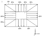
- FIG. 5 is a diagram for explaining the distribution of the first electrode 105 in the tilt direction from the horizontal plane in the display surface 201 of the display device 1 according to the first embodiment.
- FIG. 5 schematically illustrates the display surface 201 of the display device 1 as viewed from the front. As shown in the figure, in the first embodiment, the display surface 201 is divided into three parts in the vertical direction and three parts in the horizontal direction, and nine regions 207a to 207i are set. Then, the inclination direction of the first electrode 105 from the horizontal plane is changed for each of the regions 207a to 207i.
- the horizontal direction of the display surface 201 when viewed from the front is also referred to as the x-axis direction
- the vertical direction is also referred to as the y-axis direction
- a direction perpendicular to the x-axis direction and the y-axis direction (that is, a direction perpendicular to the display surface 201) is also referred to as a z-axis direction.
- the direction from the left side toward the right side toward the display surface 201 is defined as the positive direction of the x axis
- the direction from the lower side toward the upper side toward the display surface 201 is defined as the positive direction of the y axis.
- the direction corresponding to the emission direction is taken as the positive direction of the z axis.
- the inclination direction from the horizontal plane of the first electrode 105 in each of the regions 207a to 207i is schematically represented by an arrow.
- the direction of the arrow corresponds to the direction in which the height of the inclined first electrode 105 is lowered.
- the configuration example illustrated in FIG. 5 corresponds to the arrangement of the display device 1, the eyeball 203, and the optical system 205 as illustrated in FIG. 1, and the pixels arranged in the vicinity of the outer periphery of the display surface 201 of the display device 1. This corresponds to the case where a wider viewing angle characteristic is required.
- the pixel arranged in the central region 207 e of the display surface 201 is configured not to tilt the first electrode 105.
- the first electrode 105 is inclined from the horizontal plane in a direction radially toward the outer edge from the center of the display surface 201. Configured as follows.
- FIG. 4 The cross-sectional structure of the display device 1 shown in FIG. 4 corresponds to the cross section in the region 207d viewed from the negative direction of the y axis.
- FIGS. 6 and 7 show partial cross-sectional views in other regions of the display device 1.
- 6 and 7 are cross-sectional views in other regions of the display device 1 according to the first embodiment.
- 6 and 7 show a schematic partial cross section of the display device 1 as in FIG.
- the cross-sectional structure shown in FIG. 6 corresponds to the cross section in the region 207e viewed from the negative direction of the y-axis.
- the first electrode 105 is not inclined in the region 207e, as shown in FIG. 6, in the cross section in the region 207e of the display device 1, the first electrode 105 and each layer stacked thereabove are Is formed so as to be substantially parallel to the horizontal plane.
- the cross-sectional structure shown in FIG. 7 corresponds to the cross section in the region 207f viewed from the negative direction of the y-axis.
- the first electrode 105 is formed to be inclined toward the outer edge of the display surface 201, that is, to be inclined toward the positive direction of the x axis.
- each layer from the first electrode 105 to the CF layer 113 is formed to be inclined in the direction opposite to the cross section shown in FIG.
- the surface of the first electrode 105 exposed from the pixel definition film 103 (that is, the emission center of the light emitting element 110) is in the horizontal plane.
- the CF layer 113 is formed so that the center at the center and the center of the CF 113a corresponding to itself in the horizontal plane substantially coincide with each other.
- the center positions thereof are shifted. End up.
- each CF 113a corresponding to each first electrode 105 in the layer can be adjusted so as to pass through the center of the lower surface of the CF 113a. Thereby, the emitted light from each light emitting element 110 is reliably incident by the CF 113a corresponding to itself, and the occurrence of color mixing is suppressed.
- each pixel can be configured so that the outgoing light toward the outside has more desired characteristics. Therefore, for example, even when the display device 1 is arranged so as to face the small optical system 205 as shown in FIG. It becomes possible to provide an indication.
- the viewing angle characteristics of each pixel are adjusted by inclining the first electrode 105 of the light emitting element 110 from the horizontal plane in each pixel. Further, by providing a distribution in the tilt direction of the first electrode 105 in the display surface 201 of the display device 1, the viewing angle characteristics of each pixel in the display surface 201 are also distributed. That is, pixels having different viewing angle characteristics are arranged according to the position in the display surface 201. Therefore, the viewing angle characteristics required according to the application of the display device 1 can be realized for each pixel, and a higher quality display can be provided to the user.
- a distribution may be provided in the tilt direction in the display surface 201 so that the tilt direction from the horizontal plane of the first electrode 105 is outward in the pixels near the outer periphery.
- the first electrode 105 may be distributed in the tilt direction in the display surface 201 so that the tilt direction from the horizontal plane is inward.
- the viewing angle characteristics are improved by inclining the first electrode 105 from the horizontal plane as described above, as described above (1. Background to the present disclosure).
- it is not necessary to apply the configuration proposed so far for improving the viewing angle characteristics for example, narrowing of the opposing gap and reduction of the area of the light emitting surface. Therefore, it is possible to improve the viewing angle characteristics without deteriorating the light emission characteristics and the protective properties of the light emitting element 110 (OLED) and without causing a decrease in luminance.
- the display device 1 according to the embodiment can be manufactured relatively easily without significantly increasing the number of manufacturing steps. Therefore, a desired effect can be obtained without increasing the production cost.
- color correction processing may be performed by a drive circuit.
- the drive circuit can be configured more easily, and the circuit scale of the drive circuit can be further reduced.
- the inclination of the first electrode of each pixel from the horizontal plane is adjusted according to the optical system of the electronic apparatus to which the display device 1 can be applied.
- the display device 1 when designing the display device 1, it is possible to design including the optical system in the electronic apparatus. Thereby, the freedom degree of design of the display apparatus 1 and an electronic device improves. Therefore, for example, compared with the case where the display device 1 and the electronic device are separately designed, it is possible to realize a more enlarged display or to arrange the display surface 201 of the display device 1 closer to the user's eyeball 203. It becomes possible.
- the display device 1 according to the first embodiment can be suitably applied even when these arrangements in the electronic device are different. If these arrangements are different, the viewing angle characteristics required for each pixel of the display device 1 differ accordingly, so that the desired viewing angle characteristics of the first electrode 105 in the display surface 201 can be realized. What is necessary is just to set the distribution of the inclination direction from a horizontal surface.
- the display surface 201 is divided into a plurality of regions 207a to 207i, and the regions 207a to 207i are divided.
- the first embodiment is not limited to such an example.
- the display device 1 according to the first embodiment may have a distribution in the tilt direction for each pixel (see (5-2. Tilt angle and tilt direction of the first electrode from the horizontal plane in the display surface). As well as a variation of the method of forming the first electrode).
- the first electrode 105 is distributed in the tilt direction from the horizontal plane in the display surface 201.
- the first embodiment is not limited to this example.
- a distribution may be given to the inclination angle of the first electrode 105 within the display surface 201 from the horizontal plane.
- the specific distribution of the tilt angle may be appropriately set so as to realize the viewing angle characteristics required for each pixel according to the use of the display device 1.
- the display device 1 the eyeball 203, and the optical system 205 are arranged as shown in FIGS. 1 and 3, and the viewing angle characteristics in the direction toward the outside or the inside are more required for the pixels near the outer periphery.
- the inclination angle of the first electrode 105 in the display surface 201 may be distributed so that the inclination angle from the horizontal plane increases toward the outside of the display surface 201. Also, the distribution of the tilt angle may be set for each region or for each pixel in the display surface 201.
- the display device 1 is an OCCF type display device in which the CF layer 113 is formed on the first substrate 11, but the first embodiment is not limited to such an example.
- the CF layer 113 is formed on the second substrate 117, and the first substrate 101 and the second substrate 117 are disposed so that the CF layer 113 faces the light emitting element 110.
- a so-called counter-CF display device manufactured by bonding together is a so-called counter-CF display device manufactured by bonding together.
- the display device 1 has a configuration in which one pixel is formed by sub-pixels of four colors of a red pixel, a green pixel, a blue pixel, and a white pixel.
- the embodiment is not limited to this example.
- the display device 1 according to the first embodiment may have other pixel configurations.
- each first electrode is arranged such that the perpendicular from the surface of the first electrode 105 exposed from the pixel definition film 103 passes through the center of the lower surface of the CF 113 a corresponding to itself.
- the first embodiment is not limited to such an example. For example, when the inclination angle of the first electrode 105 from the horizontal plane is small, the center of the surface of the first electrode 105 exposed from the pixel definition film 103 is not adjusted without adjusting the position in the layer of the CF 113a. The amount of positional deviation from the center of the CF 113a corresponding to the first electrode 105 is not so large.
- the position of the CF 113a in the layer need not be adjusted with the inclination of the first electrode 105 from the horizontal plane.
- the display device 1 realizes color display by providing the CF 113a with respect to the light emitting element 110 that emits white light.
- the first embodiment is not limited to such an example.
- the display device 1 according to the first embodiment may not include the CF layer 113, and each light emitting element 110 is configured to emit one of red, green, and blue light, thereby performing color display. May be realized.
- the display apparatus 1 which concerns on 1st Embodiment does not need to be comprised so that a color display is realizable, and may be a display apparatus in which a monochrome display is possible.
- the display device 1 does not necessarily include the CF layer 113. Even in the case where the CF layer 113 is not provided, the viewing angle characteristics can be controlled for each pixel by having the configuration in which the first electrode 105 of each light emitting element 110 is inclined from the horizontal plane. It is possible to improve the viewing angle characteristics.
- the first electrode 105 disposed in a lower layer that hits the reflective electrode is inclined from the horizontal plane. It was.
- the first embodiment is not limited to such an example, and the display device 1 may be a bottom emission type display device.
- the second electrode 109 disposed in an upper layer functions as a reflective electrode. Therefore, in this case, the second electrode 109 may be inclined from the horizontal plane in order to control the viewing angle characteristics.
- an electrode that can function as a reflective electrode is provided. What is necessary is just to be comprised so that the surface facing the organic layer which functions as a light emission part may incline from a horizontal surface.
- the display device 1 is configured such that the first electrode 105 functions as an anode and the second electrode 109 functions as a cathode.
- the first embodiment is not limited to such an example.
- the display device 1 according to the first embodiment may be configured such that the first electrode 105 functions as a cathode and the second electrode 109 functions as an anode.
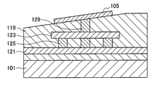
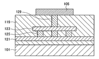
- FIG. 8 is a diagram showing a configuration in the vicinity of the first electrode 105 of the display device 1 shown in FIG. 4
- the wiring structure is provided in an interlayer insulating layer 119 provided on the first substrate 101, and the first wiring layer 121, the second wiring layer 123, the first wiring layer 121, and the second wiring layer 123 are provided. And vias 129 that electrically connect the second wiring layer 123 and the first electrode 105.
- the wiring structure is for electrically connecting a TFT (not shown) for driving the light emitting element 110 and the first electrode 105.
- the inclination angle of the first electrode 105 from the horizontal plane can be determined based on the optical viewpoint, that is, the viewing angle characteristics required for each pixel.
- the area of the first electrode 105 and the first electrode 105 It can also be determined from a structural point of view, such as the thickness of layers disposed above and below 105.
- the possible range of the inclination angle of the first electrode 105 from the horizontal plane can be determined geometrically based on the dimensions of each layer.
- the length w a of the first electrode 105 and the second wiring layer 123 in one direction (x-axis direction in the illustrated example) on the projection plane of the first electrode 105 onto the horizontal plane is 1 to 3. It is assumed that the vertical distance h 1 from the surface of the second wiring layer 123 to the lowest point of the first electrode 105 is about 800 to 2000 (nm). In this case, from the viewpoint of reliability and the like in the process, the range to obtain difference h 2 takes the vertical lowest point and the highest point of the lower surface of the first electrode 105 is about 30 ⁇ 1000 (nm). Therefore, the range in which the inclination angle ⁇ of the first electrode 105 from the horizontal plane can be taken is about 2 to 20 (°).
- the horizontal angle of the first electrode 105 in each pixel is satisfied within this range so as to satisfy the viewing angle characteristics required for each pixel determined according to the application of the display device 1 as much as possible.
- the value of the inclination angle ⁇ is determined.
- shifting amount d c of CF113a with the inclination from the horizontal plane of the first electrode 105 can be determined geometrically.
- a protective film 111 it is assumed that the thickness h 3 is configured such that the extent 500 ⁇ 3000 (nm).
- the CF 113a can be arranged such that the perpendicular from the surface of the first electrode 105 corresponding to the CF 113a exposed from the pixel definition film 103 passes through the center of the lower surface of the CF 113a.
- the shift amount d of the CF 113a in the horizontal plane direction d is about 15 to 1100 (nm).
- the structure of the first electrode 105, particularly the inclination angle from the horizontal plane has been described in more detail above.
- the specific numerical value shown above is an example to the last.
- the specific structure of the display device 1 according to the first embodiment is not limited to such an example, and the shape such as the thickness and area of each layer may be appropriately changed according to process conditions, layout rules, and the like.
- the range in which the inclination angle ⁇ of the first electrode 105 from the horizontal plane can be structurally changed can be appropriately changed according to the actual thickness, area, etc. of each layer in the display device 1.
- FIGS. 9A to 9D and FIGS. 10A to 10C A manufacturing method of the display device 1 shown in FIGS. 4 to 7 will be described with reference to FIGS. 9A to 9D and FIGS. 10A to 10C.
- a method for forming the first electrode 105 which is a characteristic configuration of the first embodiment, will be mainly described.
- As a method for forming each of the other layers various known methods used in a general method for manufacturing an organic EL display can be used, and thus description thereof is omitted here.
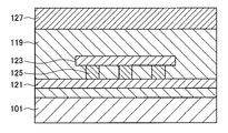
- FIGS. 9A to 9D are views for explaining a process flow when forming the first electrode 105 inclined from the horizontal plane shown in FIG. 4.
- an interlayer insulating layer 119 is laminated on a first wiring layer 121, a via 125, and a second wiring layer 123 formed on a first substrate 101, respectively.
- a resist layer 127 is formed on the interlayer insulating layer 119 so as to have different thicknesses in a horizontal plane.
- the resist layer 127 having such a shape can be realized by applying a resist material and then performing exposure using a gray scale mask (a mask in which ultraviolet transmittance is distributed in the plane).
- etch back is performed with the resist layer 127 formed.
- the etching is performed under such a condition that the selection ratio between the resist layer 127 and the interlayer insulating layer 119 is relatively small.
- an inclination is formed on the surface of the interlayer insulating layer 119 in accordance with the difference in thickness of the resist layer 127 (FIG. 9C).
- FIGS. 10A to 10C are diagrams for explaining a process flow when forming the first electrode 105 that is not inclined from the horizontal plane shown in FIG.
- Each of the steps shown in FIGS. 10A to 10C and each of the steps shown in FIGS. 9B to 9D are performed in a region where the first electrode 105 is not inclined from the horizontal plane and a region where the first electrode 105 is inclined from the horizontal plane, respectively.
- the formation process of the 1st electrode 105 is shown as a separate figure for convenience, and these processes are actually performed simultaneously.
- the interlayer insulating layer 119 is stacked on the first wiring layer 121, the via 125, and the second wiring layer 123 formed on the first substrate 101, respectively.
- a resist layer 127 is formed on the interlayer insulating layer 119.
- the resist layer 127 is formed to have a substantially uniform thickness, unlike the region where the first electrode 105 shown in FIG. 9B is inclined from the horizontal plane.
- etch back is performed with the resist layer 127 formed. Since the thickness of the resist layer 127 is substantially uniform, the surface of the interlayer insulating layer 119 after the etch back is substantially parallel to the horizontal plane (FIG. 10B).
- the manufacturing method of the display apparatus 1, especially the formation method of the 1st electrode 105 was demonstrated.
- FIG. 11 is a cross-sectional view illustrating a configuration example of the display device according to the second embodiment.
- FIG. 11 is a schematic partial cross-sectional view of the display device according to the second embodiment.
- the display device according to the second embodiment also divides the display surface 201 into nine regions 207a to 207i. Different tilt directions are set for one electrode 105 (see FIG. 5).
- the partial cross-sectional view shown in FIG. 11 corresponds to a cross-sectional view of one part in the region corresponding to the region 207d.
- the display device 1a according to the second embodiment corresponds to the display device 1 according to the first embodiment described above having a different first electrode 105 shape. Since the configuration other than this is the same as that of the display device 1, in the following description of the display device 1a according to the second embodiment, only matters different from the first embodiment will be mainly described. Detailed description of items that are the same as those in the embodiment will be omitted.
- the distribution of the thickness of the first electrode 105 causes the upper surface (the surface facing the organic layer 107) to be inclined from the horizontal plane.
- the upper surface of the first electrode 105 that is, the light emitting surface of the light emitting element 110 is inclined from the horizontal plane
- the viewing angle characteristics can be controlled for each pixel as in the first embodiment.
- the surface of the first electrode 105 exposed from the pixel definition film 103 that is, the light emission center of the light emitting element 110.
- the position of the CF 113a in the CF layer 113 may be adjusted as appropriate so that the perpendicular passes through the center of the lower surface of the CF 113a corresponding to itself.
- the range in which the inclination angle of the upper surface of the first electrode 105 from the horizontal plane can be determined based on the limit value of the thickness that the first electrode 105 can take. For example, due to process restrictions, there may be a limit value for the thickness of the first electrode 105, so the maximum value and the minimum value of the thickness and the length of the first electrode 105 in one direction on the horizontal plane (see FIG. depending on w length corresponding to a) and at 8, the inclination angle can be determined.
- the second embodiment has an upper surface of the first electrode 105 as compared with the first embodiment in which the entire first electrode 105 is inclined from the horizontal plane. It is considered that the maximum value that the inclination angle from the horizontal plane can take becomes small.
- the surface of the underlying layer on which the first electrode 105 is formed is also inclined, so that each layer above the first electrode 105 is also in the horizontal plane. It had a configuration inclined with respect to it.
- the surface of the base layer on which the first electrode 105 is formed is not inclined, so that the layers above the first electrode 105 are also substantially inclined with respect to the horizontal plane. I don't have it. Therefore, for example, when designing the configuration such as the thickness of each layer from the viewpoint of optical and process, the design of each layer may be different between the first embodiment and the second embodiment.
- the configuration according to the first embodiment is applied or the configuration according to the second embodiment is applied in consideration of the above-mentioned various differences, ease of design, and desired optics. It may be appropriately determined from the viewpoint of whether the characteristics can be realized.
- FIG. 11 A manufacturing method of the display device 1 shown in FIG. 11 will be described with reference to FIGS. 12A to 12C.
- a method of forming the first electrode 105 which is a characteristic configuration of the second embodiment, will be mainly described.
- various known methods used in a general method for manufacturing an organic EL display can be used, and thus description thereof is omitted here.
- the forming method will also be described.
- FIGS. 12A to 12C are views for explaining a process flow when forming the first electrode 105 whose upper surface shown in FIG. 11 is inclined from the horizontal plane.
- an interlayer insulating layer 119 is laminated on the first wiring layer 121, the via 125, and the second wiring layer 123 formed on the first substrate 101, respectively.
- the first electrode 105 is formed on the interlayer insulating layer 119 by forming a metal film with a uniform thickness and patterning (FIG. 12A).
- a resist layer 127 is formed on the interlayer insulating layer 119 and the first electrode 105 so as to have different thicknesses in the horizontal plane.
- the resist layer 127 having such a shape can be realized by applying a resist material and then performing exposure using a gray scale mask.
- etch back is performed with the resist layer 127 formed.
- the etching is performed under such a condition that the selection ratio between the resist layer 127 and the first electrode 105 is relatively small.
- the upper surface of the first electrode 105 is inclined with respect to the horizontal plane (FIG. 12C).
- FIGS. 13A and 13B are diagrams for explaining a process flow in forming the first electrode 105 whose upper surface is not inclined from the horizontal plane in the display device 1a according to the second embodiment.
- the upper surface of the first electrode 105 is not inclined from the horizontal plane, and the upper surface of the first electrode 105 is inclined from the horizontal plane.
- the steps of forming the first electrode 105 in the region are shown as separate drawings for convenience, and these steps are actually performed at the same time.
- an interlayer insulating layer 119 is stacked on the first wiring layer 121, the via 125, and the second wiring layer 123 formed on the first substrate 101, and the first electrode 105 is formed on the metal film. Are formed with a uniform thickness and patterned.
- a resist layer 127 is formed on the interlayer insulating layer 119 and the first electrode 105.
- the resist layer 127 has a substantially uniform thickness, unlike the region where the upper surface of the first electrode 105 shown in FIG. 12B is inclined from the horizontal plane. Formed as follows.
- etch back is performed with the resist layer 127 formed. Since the thickness of the resist layer 127 is substantially uniform, the upper surface of the first electrode 105 after the etch back is substantially parallel to the horizontal plane (FIG. 12C).
- the method for manufacturing the display device 1a particularly the method for forming the first electrode 105 has been described above.
- FIG. 14 is a cross-sectional view illustrating a configuration example of the display device according to the third embodiment.
- FIG. 14 is a schematic partial cross-sectional view of a display device according to the third embodiment.
- the display device according to the third embodiment also divides the display surface 201 into nine regions 207a to 207i, and each region 207a. In 207i to 207i, different inclination directions are set for the first electrode 105 (see FIG. 5).
- the partial cross-sectional view shown in FIG. 14 corresponds to a cross-sectional view of one part in the region corresponding to the region 207d.
- the display device 1b according to the third embodiment corresponds to the display device 1 according to the first embodiment described above in which the shape of the pixel definition film 103a is changed. Specifically, in the display device 1b, the pixel defining film 103a is formed thicker. In addition, the side wall of the opening provided corresponding to the first electrode 105 of the pixel defining film 103a has a tapered shape such that the area in the horizontal plane of the opening increases as it goes upward.
- the display device 1b has the same configuration as the display device 1 described above except that the shape of the pixel definition film 103a is different. Therefore, in the following description of the display device 1b, items different from the display device 1 will be mainly described, and detailed descriptions of items overlapping with the display device 1 will be omitted.
- the pixel definition film 103a is configured as described above, and the refractive index of the protective film 111 that fills the opening of the pixel definition film 103a provided corresponding to the first electrode 105 is the pixel definition film 103a.
- the material of the pixel definition film 103a and the protective film 111 is selected so as to be larger than the refractive index.
- Light emitted from the light emitting element 110 travels outward through the protective film 111, but with the above configuration, the light propagates through the protective film 111 on the surface of the pixel definition film 103 a facing the protective film 111. The transmitted light is reflected at least partially.
- the protective film is formed at the interface between the pixel definition film 103a and the organic layer 107. At least a part of the light propagating through 111 is reflected. That is, the surface of the pixel definition film 103a facing the protective film 111 functions as a light reflecting portion (reflector).
- the opening of the pixel definition film 103a is embedded by the protective film 111. However, in the actual structure, the opening that satisfies the above-described refractive index relationship is illustrated. A dedicated layer for embedding can be provided (see first member 51 of FIG. 20 described later).
- the side wall of the opening provided corresponding to the first electrode 105 of the pixel defining film 103a has a tapered shape such that the area of the opening gradually increases upward. Therefore, the light emitted from the light emitting element 110 toward the side wall of the opening of the pixel defining film 103a is reflected upward and is emitted from the second substrate 117 to the outside by adding a desired CF 113a.
- the display surface 201 is divided into nine regions 207a to 207i, and the tilt direction of the first electrode 105 from the horizontal plane is changed for each of the regions 207a to 207i.
- the first electrode 105 is distributed in the direction of inclination from the horizontal plane.
- the first to third embodiments are not limited to such an example, and the region setting method for changing the inclination direction of the first electrode 105 from the horizontal plane may be used for the display device 1, 1a, 1b (for example, It may be arbitrary depending on the arrangement of the optical members in the electronic apparatus on which the display devices 1, 1a, 1b are mounted.
- FIGS. 15 to 19 are diagrams for explaining another example of the setting method of the region in the display surface 201 for changing the inclination direction of the first electrode 105 from the horizontal plane.
- 15 to FIG. 19 illustrate the state of the display surface 201 of the display device 1, 1 a, 1 b as viewed from the front, as in FIG. 5, and the first electrode is provided in each region provided in the display surface 201.
- the arrow which shows the inclination direction from the horizontal surface of 105 is illustrated.
- the direction of the arrow corresponds to the direction in which the height of the inclined first electrode 105 is lowered.
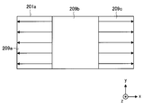
- the display surface 201a is divided into three in the horizontal direction, and three regions 209a to 209c are set. Also good.
- the pixel arranged in the central region 209b is configured not to incline the first electrode 105 from the horizontal plane.
- the pixels arranged in the other regions 209a and 209c located on both sides in the horizontal direction of the region 209b are arranged such that the first electrode 105 is inclined from the horizontal plane in the direction from the center of the display surface 201a toward the outer edge in the horizontal direction.
- Each is composed.
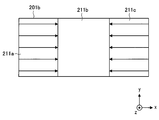
- the horizontally long display surface 201b is divided into three in the horizontal direction, and three areas 211a to 211c are set.
- the pixel arranged in the central region 211b is configured not to incline the first electrode 105 from the horizontal plane.
- the pixels arranged in the other regions 211a and 211c located on both sides of the region 209b have the first electrode 105 in the direction toward the center of the display surface 201a (that is, the direction toward the center region 211b). Each is configured to be inclined from a horizontal plane.
- the display surface 201c is divided into three in the horizontal direction, and the central area is further divided into three in the vertical direction, so that five areas 213a to 213e are set. Also good.
- the pixel arranged in the central region 213e is configured not to incline the first electrode 105 from the horizontal plane.
- the pixels arranged in the regions 213a and 213b located on both sides of the region 213e are configured such that the first electrode 105 is inclined from the horizontal plane in the direction from the center of the display surface 201a toward the outer edge in the horizontal direction. Is done.
- the pixels arranged in the regions 213c and 213d located on both sides in the vertical direction of the region 213e are configured such that the first electrode 105 is inclined from the horizontal plane in the direction from the center of the display surface 201a toward the outer edge in the vertical direction. Is done.
- the display surface 201d is divided into three in the horizontal direction and the central area is further divided into three in the vertical direction, as in the example shown in FIG. 215e is set.
- the pixel arranged in the central region 215e is configured not to incline the first electrode 105 from the horizontal plane.
- the pixels arranged in the regions 215a and 215b located on both sides in the lateral direction of the region 215e are arranged so that the first electrode 105 extends from the horizontal plane in the direction toward the center of the display surface 201a (that is, the direction toward the central region 215e). Each is configured to be inclined.
- the pixels arranged in the regions 215c and 215d located on both sides in the vertical direction of the region 215e are arranged in a direction toward the center of the display surface 201a (that is, a direction toward the center region 215e), and the first electrode 105 is disposed from the horizontal plane.
- Each is configured to be inclined.
- the display surface 201e is divided into three parts in the vertical direction and three parts in the horizontal direction, and nine regions 217a. To 217i are set.
- the pixel arranged in the central region 217e is configured not to incline the first electrode 105 from the horizontal plane.
- the pixels arranged in the other areas 217a to 217d and 217f to 217i located on the outer periphery of the display surface 201e are first in the direction toward the center of the display surface 201a (that is, the direction toward the center area 217e).
- Each of the electrodes 105 is configured to be inclined from a horizontal plane.
- the display surface 201 is divided into a plurality of regions, and the first electrode 105 is distributed in the inclination direction of the first electrode 105 in the display surface 201 by changing the inclination direction of the first electrode 105 from the horizontal plane for each region.
- the first to third embodiments are not limited to such examples.
- each pixel may have a distribution in an inclination angle and an inclination direction from the horizontal plane.
- a resist layer having a dome shape so as to cover the entire display surface 201 is formed after an interlayer insulating layer 119 serving as a base layer of the first electrode 105 is formed.
- a process of forming an on-chip lens (OCL: On Chip Lens) used in manufacturing an imager or the like can be applied. Then, etch back is performed with this dome-shaped resist layer formed.
- the etching is performed under such a condition that the selection ratio between the resist layer and the interlayer insulating layer 119 is relatively small.
- a continuous slope is formed on the surface of the lower interlayer insulating layer 119 in accordance with the difference in thickness of the resist layer 127. That is, the surface of the interlayer insulating layer 119 is also processed into a substantially dome shape.
- the first electrode 105 is formed on the interlayer insulating layer 119 after forming the via 129 for connecting to the lower second wiring layer 123 as in the process shown in FIG.
- the first electrode 105 can be formed so that the inclination angle and the inclination direction from the horizontal plane continuously change.
- the display surface 201 of the display devices 1, 1a, 1b is omitted.
- the optical system in the electronic apparatus is designed so that the center and the optical axis of the optical system and / or the eye axis of the user's eye substantially coincide. Therefore, the distribution of the tilt direction and / or tilt angle from the horizontal plane of the first electrode 105 in the display surface 201 is preferably set symmetrically with respect to the center of the display surface 201.
- the distribution in the display surface 201 of the inclination direction and / or the inclination angle from the horizontal plane of the first electrode 105 in each of the embodiments and modifications described above is symmetrical with respect to the center of the display surface 201. Therefore, it can be said that the display device according to each embodiment and each modification can be suitably mounted on various electronic devices.
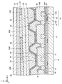
- FIG. 20 is a cross-sectional view showing a specific configuration example of the display device 1b according to the third embodiment. 20 shows a partial cross-sectional view of the display device 1b, specifically, a partial cross-sectional view of a region corresponding to the region 207d shown in FIG.
- the display device 1 b is provided on the first substrate 11 with a plurality of light emitting elements 10 that emit white light composed of OLEDs, and in an upper layer of the light emitting elements 10.
- a CF layer 33 in which CF of each color is formed corresponding to each of the light emitting elements 10.
- a second substrate 34 made of a material transparent to the light from the light emitting element 10 is disposed on the CF layer 33.
- the first substrate 11, the light emitting element 10, the CF layer 33, and the second substrate 34 correspond to the first substrate 101, the light emitting element 110, the CF layer 113, and the second substrate 117, respectively.
- the first substrate 11 is provided with TFTs 15 for driving the light emitting elements 10 corresponding to the light emitting elements 10.
- An arbitrary light emitting element 10 is selectively driven by the TFT 15. The light from the driven light emitting element 10 passes through the corresponding CF, the color is appropriately converted, and is emitted from above through the second substrate 34, thereby displaying a desired image, characters, and the like. .
- the first substrate 11 is composed of a silicon substrate.
- the second substrate 34 is made of quartz glass.
- the third embodiment is not limited to this example, and various known materials may be used as the first substrate 11 and the second substrate 34.
- the first substrate 11 and the second substrate 34 are a high strain point glass substrate, a soda glass (mixture of Na 2 O, CaO and SiO 2 ) substrate, a borosilicate glass (Na 2 O, B 2 O 3 and SiO 2).
- substrate 34 may be the same, and may differ. However, since the display device 1b is a top emission type, it is preferable that the second substrate 34 is formed of a material having high transmittance that can suitably transmit light from the light emitting element 10.
- the light emitting element 10 includes a first electrode 21, an organic layer 23 provided on the first electrode 21, and a second electrode 22 formed on the organic layer 23.
- the first electrode 21, the organic layer 23, and the second electrode 22 correspond to the first electrode 105, the organic layer 107, and the second electrode 109 described above, respectively.
- a second member 52 provided with an opening 25 so as to expose at least a part of the first electrode 21 is laminated on the first electrode 21, and the organic layer 23 is It is provided on the first electrode 21 exposed at the bottom of the opening 25. That is, the light emitting element 10 has a configuration in which the first electrode 21, the organic layer 23, and the second electrode 22 are stacked in this order in the opening 25 of the second member 52.
- This stacked structure functions as the light emitting portion 24 of each pixel. That is, the portion of the light emitting element 10 that contacts the opening 25 of the second member 52 is the light emitting surface.
- the second member 52 functions as a pixel definition film that is provided between the pixels and defines the area of the pixels.
- the second member 52 corresponds to the pixel definition film 103a described above.
- the organic layer 23 includes a light emitting layer made of an organic light emitting material and is configured to emit white light.
- the specific configuration of the organic layer 23 is not limited, and may be various known configurations.
- the organic layer 23 has a stacked structure of a hole transport layer, a light emitting layer, and an electron transport layer, a stacked structure of a hole transport layer and a light emitting layer that also serves as an electron transport layer, or a hole injection layer and a hole transport. It can be composed of a laminated structure of a layer, a light emitting layer, an electron transport layer, and an electron injection layer.
- the organic layer 23 may have a two-stage tandem structure in which a first tandem unit, a connection layer, and a second tandem unit are laminated. Good.
- the organic layer 23 may have a three or more tandem structure in which three or more tandem units are stacked.
- the organic layer 23 that emits white as a whole can be obtained by changing the luminescent color of the light emitting layer between red, green, and blue in each tandem unit.
- the organic layer 23 is formed by vacuum-depositing an organic material.
- the third embodiment is not limited to such an example, and the organic layer 23 may be formed by various known methods.
- the organic layer 23 may be formed by a physical vapor deposition method (PVD method) such as a vacuum deposition method, a printing method such as a screen printing method or an ink jet printing method, a laser absorption layer formed on a transfer substrate, and the like.
- PVD method physical vapor deposition method
- a laser transfer method in which the organic layer on the laser absorption layer is separated by irradiating a laser on the stacked structure of the organic layer and the organic layer is transferred, or various coating methods can be used.
- the first electrode 21 functions as an anode. Since the display device 1 b is a top emission type, the first electrode 21 is formed of a material that can reflect light from the organic layer 23. In the illustrated configuration example, the first electrode 21 is formed of an alloy of aluminum and neodymium (Al—Nd alloy). The film thickness of the first electrode 21 is, for example, about 0.1 ⁇ m to 1 ⁇ m. However, the third embodiment is not limited to such an example, and the first electrode 21 is made of various known materials that are used as a material for a light reflecting electrode that functions as an anode in a general organic EL display. Can be formed. Further, the film thickness of the first electrode 21 is not limited to the above example, and the first electrode 21 can be appropriately formed within a film thickness range generally employed in an organic EL display.
- the first electrode 21 includes platinum (Pt), gold (Au), silver (Ag), chromium (Cr), tungsten (W), nickel (Ni), copper (Cu), iron (Fe), cobalt ( Co) or a metal having a high work function such as tantalum (Ta), or an alloy (for example, 0.3% by mass to 1% by mass of palladium (Pd) and 0.3% by mass to 1% by mass of silver as a main component)
- a metal having a high work function such as tantalum (Ta), or an alloy (for example, 0.3% by mass to 1% by mass of palladium (Pd) and 0.3% by mass to 1% by mass of silver as a main component)
- an Ag—Pd—Cu alloy containing 1% copper or an Al—Nd alloy for example, an Ag—Pd—Cu alloy containing 1% copper or an Al—Nd alloy.
- a conductive material having a small work function value and high light reflectance such as aluminum or an alloy containing aluminum can be used
- the first electrode 21 has a hole injection property such as an oxide of indium and tin (ITO) or an oxide of indium and zinc (IZO) on a highly reflective film such as a dielectric multilayer film or aluminum. It is also possible to have a structure in which transparent conductive materials excellent in thickness are laminated.
- ITO indium and tin
- IZO oxide of indium and zinc
- the second electrode 22 functions as a cathode. Since the display device 1 b is a top emission type, the second electrode 22 is formed of a material that can transmit light from the organic layer 23. In the illustrated configuration example, the second electrode 22 is formed of an alloy of magnesium and silver (Mg—Ag alloy). The film thickness of the second electrode 22 is, for example, about 10 nm. However, the third embodiment is not limited to this example, and the second electrode 22 is made of various known materials that are used as a material of a light transmission side electrode that functions as a cathode in a general organic EL display. Can be formed. Further, the film thickness of the second electrode 22 is not limited to the above example, and the second electrode 22 can be appropriately formed within a film thickness range generally employed in an organic EL display.
- the second electrode 22 is made of aluminum, silver, magnesium, calcium (Ca), sodium (Na), strontium (Sr), an alloy of alkali metal and silver, or an alloy of alkaline earth metal and silver (for example, magnesium). And an alloy of Mg and Ag (Mg—Ag alloy), an alloy of magnesium and calcium (Mg—Ca alloy), an alloy of aluminum and lithium (Al—Li alloy), and the like.
- the thickness of the second electrode 22 is, for example, about 4 nm to 50 nm.
- the second electrode 22 may have a structure in which the material layer described above and a transparent electrode made of, for example, ITO or IZO (for example, a thickness of about 30 nm to 1 ⁇ m) are stacked from the organic layer 23 side.
- a transparent electrode made of, for example, ITO or IZO (for example, a thickness of about 30 nm to 1 ⁇ m)
- the thickness of the material layer described above can be reduced to, for example, about 1 nm to 4 nm.
- the 2nd electrode 22 may be comprised only with a transparent electrode.
- a bus electrode (auxiliary electrode) made of a low resistance material such as aluminum, aluminum alloy, silver, silver alloy, copper, copper alloy, gold, or gold alloy is provided for the second electrode 22, and the second electrode 22 as a whole. The resistance may be reduced.
- the first electrode 21 and the second electrode 22 are formed by depositing a material by a predetermined thickness by a vacuum evaporation method and then patterning the film by an etching method.
- the third embodiment is not limited to this example, and the first electrode 21 and the second electrode 22 may be formed by various known methods. Examples of the method for forming the first electrode 21 and the second electrode 22 include an electron beam vapor deposition method, a hot filament vapor deposition method, a vapor deposition method including a vacuum vapor deposition method, a sputtering method, a chemical vapor deposition method (CVD method), and an organic method.
- MOCVD Metal chemical vapor deposition
- various printing methods for example, screen printing, ink jet printing, or metal mask printing
- plating (electroplating) Method for example, electroless plating method, etc.
- lift-off method laser ablation method, sol-gel method and the like.
- the first electrode 21 is formed so as to be inclined with respect to the horizontal plane, for example, by the method described with reference to FIGS. 9A to 9D in (2-3. Manufacturing method) above.
- the second member 52 is formed by depositing SiO 2 to a predetermined thickness by a CVD method and then patterning the SiO 2 film using a photolithography technique and an etching technique.
- the material of the second member 52 is not limited to this example, and various materials having insulating properties can be used as the material of the second member 52.
- examples of the material constituting the second member 52 include SiO 2 , MgF, LiF, polyimide resin, acrylic resin, fluororesin, silicone resin, fluoropolymer, and silicone polymer.
- the second member 52 is formed of a material having a refractive index lower than that of the material of the first member 51.
- the first electrode 21 constituting the light emitting element 10 is provided on the interlayer insulating layer 16 made of SiON.
- the interlayer insulating layer 16 covers the light emitting element driving unit formed on the first substrate 11.
- the interlayer insulating layer 16 corresponds to the interlayer insulating layer 119 described above.
- the light emitting element driving unit is composed of a plurality of TFTs 15.
- one TFT 15 is provided for one light emitting element 10.
- the TFT 15 includes a gate electrode 12 formed on the first substrate 11, a gate insulating film 13 formed on the first substrate 11 and the gate electrode 12, and a semiconductor layer 14 formed on the gate insulating film 13.
- the In the semiconductor layer 14, a region located immediately above the gate electrode 12 functions as a channel region 14A, and a region positioned so as to sandwich the channel region 14A functions as a source / drain region 14B.
- the TFT 15 is a bottom gate type, but the third embodiment is not limited to this example, and the TFT 15 may be a top gate type.
- An interlayer insulating layer 16 (a lower interlayer insulating layer 16A and an upper interlayer insulating layer 16B) having two layers is laminated on the upper layer of the semiconductor layer 14 by a CVD method.
- the source / drain region 14B is exposed to a portion corresponding to the source / drain region 14B of the lower interlayer insulating layer 16A using, for example, a photolithography technique and an etching technique.
- a contact hole 17 is provided in the substrate, and a wiring 18 made of aluminum is formed so as to fill the contact hole 17.
- the wiring 18 is formed by combining, for example, a vacuum deposition method and an etching method.
- the upper interlayer insulating layer 16B is laminated.
- the wiring 18 schematically indicates a wiring structure including the first wiring layer 121, the second wiring layer 123, the via 125, and the via 129 described above.
- a contact hole 19 is provided in a portion of the upper interlayer insulating layer 16B where the wiring 18 is provided so as to expose the wiring 18 by using, for example, a photolithography technique and an etching technique.
- the first electrode 21 of the light emitting element 10 is formed, the first electrode 21 is formed so as to be in contact with the wiring 18 through the contact hole 19.
- the first electrode 21 of the light emitting element 10 is electrically connected to the source / drain region 14B of the TET 15 via the wiring 18.
- the gate electrode 12 of the TFT 15 is connected to a scanning circuit (not shown).
- each TFT 15 When a current is applied from the scanning circuit to each TFT 15 at an appropriate timing, each TFT 15 is driven, and each light emitting element 10 emits light so that a desired image, character, or the like is displayed as a whole. Since various known methods can be used as a driving method of the TFT 15 for obtaining an appropriate display (that is, a driving method of the display device 1b), detailed description thereof is omitted here.
- the interlayer insulating layer 16 is made of SiON, but the third embodiment is not limited to this example.
- the interlayer insulating layer 16 may be formed of various known materials that can be used as an interlayer insulating layer in a general organic EL display.
- a SiO 2 material for example, SiO 2 , BPSG, PSG, BSG, AsSG, PbSG, SiON, SOG (spin on glass), low melting glass, glass paste, etc.
- SiN materials and insulating resins for example, polyimide resins, novolac resins, acrylic resins, polybenzoxazoles, etc.
- insulating resins for example, polyimide resins, novolac resins, acrylic resins, polybenzoxazoles, etc.
- the method for forming the interlayer insulating layer 16 is not limited to the above example, and the interlayer insulating layer 16 can be formed by a known method such as a CVD method, a coating method, a sputtering method, or various printing methods. . Furthermore, in the above example, the wiring 18 is formed by forming and patterning aluminum by vacuum deposition and etching, but the third embodiment is not limited to such an example. The wiring 18 may be formed by forming and patterning various materials used as wiring in a general organic EL display by various methods.
- the opening 25 provided in the second member 52 of the light emitting element 10 is formed so that the side wall thereof has a tapered shape inclined so that the opening area increases as it goes upward.
- the first member 51 is embedded in the opening 25. That is, the first member 51 is a layer that is provided immediately above the light emitting surface of the light emitting element 10 and that propagates light emitted from the light emitting element 10 upward.
- the first member 51 has a substantially trapezoidal cross-sectional shape in the stacking direction (that is, the cross-sectional shape shown in the drawing), and a bottom surface on the upper side. Has a truncated pyramid shape.
- the first member 51 is formed by depositing Si 1-x N x by vacuum deposition so as to fill the opening 25, and then the surface of the Si 1-x N x film is formed by chemical mechanical polishing (CMP method) or the like. It is formed by flattening.
- the material of the first member 51 is not limited to this example, and as the material of the first member 51, various materials having insulating properties can be used.
- the material constituting the first member 51 includes Si 1-x N x , ITO, IZO, TiO 2 , Nb 2 O 5 , bromine-containing polymer, sulfur-containing polymer, titanium-containing polymer, or zirconium-containing polymer. Can be mentioned.
- the method for forming the first member 51 is not limited to this example, and various known methods may be used as the method for forming the first member 51.
- the first member 51 and the second member 52 have a refractive index n 1 and a refractive index n 2 of the second member 52 satisfying the relationship of n 1 > n 2 .
- the material of the member 51 and the second member 52 is selected.
- the light propagated through the first member 51 on the surface of the second member 52 facing the first member 51 by selecting the material of the first member 51 and the second member 52 so that the refractive index satisfies the above relationship. Will be at least partially reflected.
- the organic layer 23 and the second electrode 22 of the light emitting element 10 are formed between the first member 51 and the second member 52, the second member 52 and the organic layer 23 At the interface, at least a part of the light propagated through the first member 51 is reflected. That is, the surface of the second member 52 facing the first member 51 functions as the reflector 53.
- the first member 51 is provided immediately above the light emitting surface of the light emitting element 10 as described above.
- the first member 51 has a truncated cone shape with the bottom surface facing upward. Therefore, the light emitted from the light emitting surface of the light emitting element 10 is reflected upward by the interface between the first member 51 and the second member 52, that is, the reflector 53, which is the light emitting direction.
- the reflector 53 it is possible to improve the extraction efficiency of the emitted light from the light emitting element 10, and to improve the luminance of the entire display device 1b. .
- the refractive indexes of the first member 51 and the second member 52 are n 1 -n 2. It is preferable to satisfy the relationship of ⁇ 0.20. More preferably, it is desirable that the refractive indexes of the first member 51 and the second member 52 satisfy a relationship of n 1 ⁇ n 2 ⁇ 0.30. Furthermore, in order to further improve the extraction efficiency of the emitted light from the light emitting element 10, the shape of the first member 51 is 0.5 ⁇ R 1 / R 2 ⁇ 0.8 and 0.5 ⁇ H / R. It is preferable to satisfy the relationship 1 ⁇ 0.8.
- R 1 is the diameter of the light incident surface of the first member 51 (that is, the portion facing downward in the stacking direction and facing the light emitting surface of the light emitting element 10), and R 2 is the first member 51.
- the diameter of the light exit surface (ie, the surface facing upward in the stacking direction), H is the distance (height in the stacking direction) between the bottom surface and the top surface when the first member 51 is regarded as a truncated cone. .
- the protective film 31 and the flattening film 32 are laminated in this order on the flattened first member 51.
- the protective film 31 corresponds to the protective film 111 described above.
- the planarization film 32 can be formed on the protective film 31 (that is, the protective film 111).
- the protective film 31 is formed, for example, by stacking Si 1-y N y by a predetermined film thickness (about 3.0 ⁇ m) by vacuum deposition.
- the planarizing film 32 is formed, for example, by laminating SiO 2 by a predetermined film thickness (about 2.0 ⁇ m) by a CVD method and planarizing the surface by a CMP method or the like.
- the material and film thickness of the protective film 31 and the planarizing film 32 are not limited to this example, and the protective film 31 and the planarizing film 32 are used as a protective film and a planarizing film for a general organic EL display.
- the film may be appropriately formed so as to have a film thickness generally employed in an organic EL display.
- the refractive index n 3 of the protective film 31 is equal to the refractive index n 1 of the first member 51 or smaller than the refractive index n 1 of the first member 51.
- the material of the protective film 31 is selected.
- the refractive index n 3 of the protective film 31 the absolute value of the difference between the refractive index n 4 of the planarization film 32 is 0.30 or less, more preferably to be 0.20 or less, the protective film 31 and the material of the planarizing film 32 are selected.
- the light emitted from the light emitting element 10 is emitted from the interface between the first member 51 and the protective film 31, and between the protective film 31 and the planarizing film 32. Can be suppressed from being reflected or scattered at the interface, and the light extraction efficiency can be further improved.
- the configuration from the first substrate 11 to the protective film 31 of the display device 1, particularly the configuration of the reflector 53, is, for example, a display device disclosed in Japanese Patent Application Laid-Open No. 2013-191533, which is a prior application by the present applicant.
- the configuration can be applied.
- a CF layer 33 is formed on the planarizing film 32.
- the CF layer 33 corresponds to the CF layer 113 described above.
- the CF layer 33 is formed so that each color CF (red CF33R, green CF33R, and blue CF33B) having a predetermined area is provided for each of the light emitting elements 10.
- the CF layer 33 can be formed, for example, by exposing and developing a resist material in a predetermined shape using a photolithography technique.
- the film thickness of the CF layer 33 is, for example, about 2 ⁇ m.
- the material, the forming method, and the film thickness of the CF layer 33 are not limited to such examples, and the CF layer 33 can be variously known depending on various known materials used as a CF layer of a general organic EL display. According to this method, the film may be appropriately formed so as to have a film thickness generally employed in an organic EL display.
- the second substrate 34 is bonded to the upper layer of the CF layer 33 via a sealing resin film 35 such as an epoxy resin, whereby the display device 1b is manufactured.
- the thickness of the sealing resin film 35 is appropriately adjusted so that the upper surface of the second substrate 34 serving as the display surface 201 of the display device 1b is substantially parallel to the horizontal plane.
- the material of the sealing resin film 35 is not limited to this example, and the material of the sealing resin film 35 is highly transmissive with respect to the light emitted from the light emitting element 10, and the CF layer 33 and the upper layer located in the lower layer.
- Appropriately selected in consideration of excellent adhesiveness with the second substrate 34 positioned and low reflectivity at the interface between the CF layer 33 positioned in the lower layer and the second substrate 34 positioned in the upper layer May be.
- the specific configuration example of the display device 1b according to the third embodiment has been described above. Note that a specific configuration example of the display device according to each embodiment and each modification of the present disclosure is not limited to such an example.
- As the material, film thickness, and formation method of each layer constituting the display device according to each embodiment and each modification various conditions generally used when forming the layer in an organic EL display are used. be able to.
- FIG. 21 is a diagram illustrating an appearance of a smartphone as an example of an electronic apparatus to which the display device according to each embodiment and each modification may be applied.
- the smartphone 301 includes an operation unit 303 that includes buttons and receives an operation input by a user, and a display unit 305 that displays various types of information.
- the display unit 305 can be configured by a display device according to each embodiment and each modification.
- FIGS. 22 and 23 are views showing the appearance of a digital camera, which is another example of an electronic apparatus to which the display device according to each embodiment and each modification can be applied.
- FIG. 22 shows the appearance of the digital camera 311 viewed from the front (subject side)
- FIG. 23 shows the appearance of the digital camera 311 viewed from the rear.
- the digital camera 311 displays a main body (camera body) 313, an interchangeable lens unit 315, a grip 317 held by a user at the time of shooting, and various types of information.
- It has a monitor 319 and an EVF 321 that displays a through image observed by the user at the time of shooting.
- the monitor 319 and the EVF 321 can be configured by the display device according to each embodiment and each modification.
- FIG. 24 is a diagram illustrating an appearance of an HMD, which is another example of an electronic device to which the display device according to each embodiment and each modification may be applied.
- the HMD 331 includes a glasses-shaped display unit 333 that displays various types of information, and an ear hooking unit 335 that is hooked on the user's ear when worn.
- the said display part 333 may be comprised by the display apparatus which concerns on each embodiment and each modification.
- electronic devices to which the display device according to each embodiment and each modification can be applied are not limited to those exemplified above, and the display devices include a television device, an electronic book, a PDA, a notebook PC, and a video camera.
- the present invention can be applied to display devices mounted on electronic devices in various fields that perform display based on image signals input from the outside or image signals generated internally, such as HMDs and game machines.
- each configuration that can be included in the display device according to each embodiment and each configuration that can be included in the display device according to each modification described above can be applied in combination with each other as much as possible.
- the reflector structure provided in the display device 1b according to the third embodiment may be applied to the display device 1a according to the second embodiment.
- the display device to be an object of the present disclosure may be various display devices, such as an inorganic EL display and a plasma display, as long as the light emitting portion is formed by sandwiching a light emitting layer between two electrodes. . Also in these other display devices, at least in a partial region in the display surface, the surface facing the light emitting layer of the electrode functioning as the reflective electrode in the light emitting portion is inclined from the surface perpendicular to the stacking direction. By configuring the light emitting unit, it is possible to obtain the same effects as those of the above-described embodiments.
- the surface of the first electrode facing the light emitting layer is inclined toward the outer edge of the display surface.
- the display device according to (2). In the region near the outer periphery, the surface of the first electrode facing the light emitting layer is inclined toward the center of the display surface.
- the display device according to (2). (5) The distribution in the tilt direction of the first electrode in the display surface is symmetric with respect to the center of the display surface.
- the display surface is divided into a plurality of regions, and the tilt direction of the first electrode is different for each region.
- the display device according to any one of (1) to (5). (7) The tilt direction of the first electrode is different for each pixel.
- the display device according to any one of (1) to (5).
- the inclination angle of the first electrode further has a distribution in the display surface.
- the display device according to any one of (1) to (7).
- the inclination angle of the first electrode is increased toward the outer edge in the display surface.
- the display device according to (8).
- the distribution of the inclination angle of the first electrode in the display surface is symmetric with respect to the center of the display surface.
- the display device according to (8) or (9).
- (11) The display surface is divided into a plurality of regions, and the tilt angle of the first electrode is different for each region.
- the display device according to any one of (8) to (10).
- (12) The inclination angle of the first electrode is different for each pixel.
- the display device according to any one of (8) to (10).
- the upper surface of the underlayer on which the first electrode is formed has an inclination, whereby the first electrode is inclined;
- the display device Providing directly above the light emitting part, and having a substantially truncated cone shape in which the cross-sectional area in the in-plane direction perpendicular to the stacking direction gradually increases toward the upper side, propagates the emitted light from the light emitting part A first member that, A second member provided between the first member and the first member between the adjacent light emitting portions; Further comprising The refractive index of the first member is larger than the refractive index of the second member,
- the display device according to any one of (1) to (15).
- the light emitting part is a light emitting element composed of an organic light emitting diode
- the display device is an organic EL display.
- the display device according to any one of (1) to (16).
- a display device for performing display based on an image signal With The display device A plurality of light emitting portions formed on the substrate; Have The light emitting portion has a configuration in which a light emitting layer is sandwiched between a first electrode functioning as a reflective electrode and a second electrode in the stacking direction, At least in a partial region within the display surface, the surface of the first electrode facing the light emitting layer is inclined from a surface perpendicular to the stacking direction, The tilt direction of the first electrode has a distribution in the display surface. Electronics.
Landscapes
- Physics & Mathematics (AREA)
- Optics & Photonics (AREA)
- General Physics & Mathematics (AREA)
- Engineering & Computer Science (AREA)
- Theoretical Computer Science (AREA)
- Electroluminescent Light Sources (AREA)
- Devices For Indicating Variable Information By Combining Individual Elements (AREA)
Abstract
Le problème décrit par la présente invention est réaliser des améliorations dans des caractéristiques d'angle de visualisation possibles. La solution décrite par l'invention concerne un dispositif d'affichage comportant une pluralité d'unités de sortie de lumière formées sur un substrat : les unités de sortie de lumière présentant une structure dans laquelle une couche électroluminescente est prise en sandwich entre une première électrode fonctionnant en tant qu'électrode réfléchissante et une seconde électrode dans la direction de stratification ; dans au moins une partie d'une région à l'intérieur d'une surface d'affichage, la surface de la première électrode faisant face à la couche électroluminescente est inclinée à partir d'un plan perpendiculaire à la direction de stratification ; et la direction d'inclinaison de la première électrode présente une distribution à l'intérieur de la surface d'affichage.
Priority Applications (3)
| Application Number | Priority Date | Filing Date | Title |
|---|---|---|---|
| US16/078,801 US11107372B2 (en) | 2016-03-31 | 2017-03-21 | Display device and electronic apparatus |
| JP2018509079A JP6919647B2 (ja) | 2016-03-31 | 2017-03-21 | 表示装置及び電子機器 |
| CN201780019512.4A CN108780622B (zh) | 2016-03-31 | 2017-03-21 | 显示装置和电子设备 |
Applications Claiming Priority (2)
| Application Number | Priority Date | Filing Date | Title |
|---|---|---|---|
| JP2016069880 | 2016-03-31 | ||
| JP2016-069880 | 2016-03-31 |
Publications (1)
| Publication Number | Publication Date |
|---|---|
| WO2017169961A1 true WO2017169961A1 (fr) | 2017-10-05 |
Family
ID=59964286
Family Applications (1)
| Application Number | Title | Priority Date | Filing Date |
|---|---|---|---|
| PCT/JP2017/011144 Ceased WO2017169961A1 (fr) | 2016-03-31 | 2017-03-21 | Dispositif d'affichage et dispositif électronique |
Country Status (4)
| Country | Link |
|---|---|
| US (1) | US11107372B2 (fr) |
| JP (1) | JP6919647B2 (fr) |
| CN (1) | CN108780622B (fr) |
| WO (1) | WO2017169961A1 (fr) |
Cited By (7)
| Publication number | Priority date | Publication date | Assignee | Title |
|---|---|---|---|---|
| CN108461526A (zh) * | 2018-03-22 | 2018-08-28 | 上海天马有机发光显示技术有限公司 | 有机发光显示面板及其制备方法、有机发光显示装置 |
| KR20190061887A (ko) * | 2017-11-28 | 2019-06-05 | 엘지디스플레이 주식회사 | 개인 몰입형 장치 및 그 표시장치 |
| KR20190063609A (ko) * | 2017-11-30 | 2019-06-10 | 엘지디스플레이 주식회사 | 표시장치 및 이를 이용한 안경형 증강현실기기 |
| KR20190064533A (ko) * | 2019-02-01 | 2019-06-10 | 엘지디스플레이 주식회사 | 표시장치 및 이를 이용한 안경형 증강현실기기 |
| JP2021124538A (ja) * | 2020-01-31 | 2021-08-30 | キヤノン株式会社 | 画像観察装置 |
| JP2021533523A (ja) * | 2018-08-06 | 2021-12-02 | 京東方科技集團股▲ふん▼有限公司Boe Technology Group Co., Ltd. | 表示パネル、表示装置及び表示パネルの作製方法 |
| JP2022063741A (ja) * | 2020-10-12 | 2022-04-22 | キヤノン株式会社 | 表示装置 |
Families Citing this family (9)
| Publication number | Priority date | Publication date | Assignee | Title |
|---|---|---|---|---|
| CN110212012B (zh) * | 2019-07-12 | 2022-02-25 | 昆山国显光电有限公司 | 一种显示面板和显示装置 |
| CN110854281B (zh) * | 2019-11-26 | 2022-08-19 | 京东方科技集团股份有限公司 | 折叠显示面板及其制备方法 |
| CN110828535B (zh) * | 2019-12-20 | 2022-09-27 | 武汉天马微电子有限公司 | 一种阵列基板、显示面板和显示装置 |
| CN111430416A (zh) * | 2020-03-31 | 2020-07-17 | 武汉天马微电子有限公司 | 一种显示面板及其制作方法 |
| CN111816787A (zh) * | 2020-06-30 | 2020-10-23 | 合肥维信诺科技有限公司 | 一种显示面板和显示装置 |
| CN112038493B (zh) * | 2020-08-17 | 2022-05-31 | 武汉华星光电半导体显示技术有限公司 | 一种显示面板及显示装置 |
| CN114914271A (zh) * | 2021-02-10 | 2022-08-16 | 北京京东方技术开发有限公司 | 一种显示面板 |
| KR20230089875A (ko) * | 2021-12-14 | 2023-06-21 | 엘지디스플레이 주식회사 | 발광 표시 장치 |
| KR20260028997A (ko) * | 2024-08-23 | 2026-03-04 | 엘지디스플레이 주식회사 | 표시 장치 |
Citations (8)
| Publication number | Priority date | Publication date | Assignee | Title |
|---|---|---|---|---|
| JPH08340546A (ja) * | 1995-04-13 | 1996-12-24 | Canon Inc | 表示装置 |
| JP2005331665A (ja) * | 2004-05-19 | 2005-12-02 | Seiko Epson Corp | 電気光学装置及びその製造方法、並びに電子機器 |
| JP2010217581A (ja) * | 2009-03-17 | 2010-09-30 | Sharp Corp | 表示装置およびその製造方法 |
| JP2012253014A (ja) * | 2011-05-12 | 2012-12-20 | Semiconductor Energy Lab Co Ltd | 発光装置、及び発光装置を用いた電子機器 |
| US20130099258A1 (en) * | 2011-10-24 | 2013-04-25 | Samsung Mobile Display Co., Ltd. | Organic Light Emitting Diode Display |
| WO2013099276A1 (fr) * | 2011-12-28 | 2013-07-04 | パナソニック株式会社 | Panneau d'affichage électroluminescent organique et procédé de fabrication de celui-ci |
| JP2015005386A (ja) * | 2013-06-20 | 2015-01-08 | セイコーエプソン株式会社 | 電気光学装置及び電子機器 |
| JP2015149231A (ja) * | 2014-02-07 | 2015-08-20 | 株式会社ジャパンディスプレイ | 有機el表示装置 |
Family Cites Families (20)
| Publication number | Priority date | Publication date | Assignee | Title |
|---|---|---|---|---|
| US5689321A (en) | 1995-04-13 | 1997-11-18 | Canon Kabushiki Kaisha | Display apparatus |
| JP2002008870A (ja) | 2000-06-20 | 2002-01-11 | Sony Corp | 表示装置 |
| JP4258154B2 (ja) | 2002-02-28 | 2009-04-30 | パナソニック株式会社 | 有機エレクトロルミネッセンス素子、それを用いた画像形成装置、携帯端末、有機エレクトロルミネッセンス素子の製造方法 |
| KR100869810B1 (ko) * | 2007-08-02 | 2008-11-21 | 삼성에스디아이 주식회사 | 표시 장치 |
| JP2011018468A (ja) | 2009-07-07 | 2011-01-27 | Sharp Corp | 有機el表示装置 |
| JP2013008663A (ja) * | 2011-05-24 | 2013-01-10 | Canon Inc | 表示装置 |
| KR101811305B1 (ko) * | 2011-07-04 | 2017-12-27 | 삼성디스플레이 주식회사 | 유기 발광 표시 장치 및 유기 발광 표시 장치 제조 방법 |
| JP6082907B2 (ja) * | 2012-02-17 | 2017-02-22 | 株式会社Joled | 表示装置及び表示装置の製造方法 |
| US9308858B2 (en) * | 2012-07-13 | 2016-04-12 | Lg Innotek Co., Ltd. | Lamp unit and lighting system for vehicle |
| KR20140033671A (ko) * | 2012-09-10 | 2014-03-19 | 삼성디스플레이 주식회사 | 유기발광 표시장치 및 그 제조 방법 |
| KR20140041119A (ko) * | 2012-09-27 | 2014-04-04 | 삼성디스플레이 주식회사 | 유기 발광 표시 장치 |
| KR102056864B1 (ko) * | 2013-04-09 | 2019-12-18 | 삼성디스플레이 주식회사 | 미러 기능을 구비한 유기 발광 표시 장치 |
| KR101485166B1 (ko) * | 2013-04-25 | 2015-01-22 | 삼성디스플레이 주식회사 | 유기 발광 표시 장치 및 마스크 유닛 |
| US20150176772A1 (en) * | 2013-12-20 | 2015-06-25 | Ge Lighting Solutions Llc | Spherical shaped led array for an omni-directional light source |
| EP3127327B1 (fr) * | 2014-03-31 | 2019-07-31 | Telefonaktiebolaget LM Ericsson (publ) | Procédé et noeud de centre de service de diffusion/multidiffusion (bm-sc), pour la fourniture d'un service sur demande |
| KR20160010708A (ko) * | 2014-07-17 | 2016-01-28 | 삼성디스플레이 주식회사 | 유기발광 디스플레이 장치 |
| US10134803B2 (en) * | 2015-01-23 | 2018-11-20 | Vuereal Inc. | Micro device integration into system substrate |
| CN104638147B (zh) * | 2015-03-04 | 2017-01-25 | 京东方科技集团股份有限公司 | 一种像素界定层及oled器件 |
| CN104733505B (zh) * | 2015-03-19 | 2017-11-24 | 京东方科技集团股份有限公司 | 发光显示器的像素界定层及其制作方法 |
| JP6697299B2 (ja) * | 2015-04-01 | 2020-05-20 | 株式会社半導体エネルギー研究所 | 有機金属錯体、発光素子、発光装置、電子機器、および照明装置 |
-
2017
- 2017-03-21 WO PCT/JP2017/011144 patent/WO2017169961A1/fr not_active Ceased
- 2017-03-21 US US16/078,801 patent/US11107372B2/en active Active
- 2017-03-21 JP JP2018509079A patent/JP6919647B2/ja active Active
- 2017-03-21 CN CN201780019512.4A patent/CN108780622B/zh active Active
Patent Citations (8)
| Publication number | Priority date | Publication date | Assignee | Title |
|---|---|---|---|---|
| JPH08340546A (ja) * | 1995-04-13 | 1996-12-24 | Canon Inc | 表示装置 |
| JP2005331665A (ja) * | 2004-05-19 | 2005-12-02 | Seiko Epson Corp | 電気光学装置及びその製造方法、並びに電子機器 |
| JP2010217581A (ja) * | 2009-03-17 | 2010-09-30 | Sharp Corp | 表示装置およびその製造方法 |
| JP2012253014A (ja) * | 2011-05-12 | 2012-12-20 | Semiconductor Energy Lab Co Ltd | 発光装置、及び発光装置を用いた電子機器 |
| US20130099258A1 (en) * | 2011-10-24 | 2013-04-25 | Samsung Mobile Display Co., Ltd. | Organic Light Emitting Diode Display |
| WO2013099276A1 (fr) * | 2011-12-28 | 2013-07-04 | パナソニック株式会社 | Panneau d'affichage électroluminescent organique et procédé de fabrication de celui-ci |
| JP2015005386A (ja) * | 2013-06-20 | 2015-01-08 | セイコーエプソン株式会社 | 電気光学装置及び電子機器 |
| JP2015149231A (ja) * | 2014-02-07 | 2015-08-20 | 株式会社ジャパンディスプレイ | 有機el表示装置 |
Cited By (15)
| Publication number | Priority date | Publication date | Assignee | Title |
|---|---|---|---|---|
| US10935784B2 (en) | 2017-11-28 | 2021-03-02 | Lg Display Co., Ltd. | Personal immersive device and display thereof |
| KR20190061887A (ko) * | 2017-11-28 | 2019-06-05 | 엘지디스플레이 주식회사 | 개인 몰입형 장치 및 그 표시장치 |
| KR102617230B1 (ko) * | 2017-11-28 | 2023-12-21 | 엘지디스플레이 주식회사 | 개인 몰입형 장치 및 그 표시장치 |
| KR20190063609A (ko) * | 2017-11-30 | 2019-06-10 | 엘지디스플레이 주식회사 | 표시장치 및 이를 이용한 안경형 증강현실기기 |
| KR102083459B1 (ko) * | 2017-11-30 | 2020-03-04 | 엘지디스플레이 주식회사 | 표시장치 및 이를 이용한 안경형 증강현실기기 |
| US10741614B2 (en) | 2017-11-30 | 2020-08-11 | Lg Display Co., Ltd. | Display device having a sloped insulating layer supporting an OLED array as used in eyeglasses-like augmented reality device |
| CN108461526A (zh) * | 2018-03-22 | 2018-08-28 | 上海天马有机发光显示技术有限公司 | 有机发光显示面板及其制备方法、有机发光显示装置 |
| JP2021533523A (ja) * | 2018-08-06 | 2021-12-02 | 京東方科技集團股▲ふん▼有限公司Boe Technology Group Co., Ltd. | 表示パネル、表示装置及び表示パネルの作製方法 |
| JP7392239B2 (ja) | 2018-08-06 | 2023-12-06 | 京東方科技集團股▲ふん▼有限公司 | 表示パネル、表示装置及び表示パネルの作製方法 |
| KR102083464B1 (ko) * | 2019-02-01 | 2020-03-02 | 엘지디스플레이 주식회사 | 표시장치 및 이를 이용한 안경형 증강현실기기 |
| KR20190064533A (ko) * | 2019-02-01 | 2019-06-10 | 엘지디스플레이 주식회사 | 표시장치 및 이를 이용한 안경형 증강현실기기 |
| JP2021124538A (ja) * | 2020-01-31 | 2021-08-30 | キヤノン株式会社 | 画像観察装置 |
| JP7486964B2 (ja) | 2020-01-31 | 2024-05-20 | キヤノン株式会社 | 画像観察装置 |
| JP2022063741A (ja) * | 2020-10-12 | 2022-04-22 | キヤノン株式会社 | 表示装置 |
| JP7198250B2 (ja) | 2020-10-12 | 2022-12-28 | キヤノン株式会社 | 表示装置 |
Also Published As
| Publication number | Publication date |
|---|---|
| US11107372B2 (en) | 2021-08-31 |
| JPWO2017169961A1 (ja) | 2019-02-14 |
| CN108780622A (zh) | 2018-11-09 |
| JP6919647B2 (ja) | 2021-08-18 |
| CN108780622B (zh) | 2022-03-04 |
| US20190066546A1 (en) | 2019-02-28 |
Similar Documents
| Publication | Publication Date | Title |
|---|---|---|
| US12235476B2 (en) | Display device and electronic apparatus | |
| JP6919647B2 (ja) | 表示装置及び電子機器 | |
| US12225763B2 (en) | Display device and electronic apparatus including pixel defining film and reflector above and over light reflecting surface of pixel defining film | |
| JP7014186B2 (ja) | 表示装置、電子機器、及び表示装置の製造方法 | |
| CN113809138A (zh) | 显示装置和电子设备 | |
| CN118383083A (zh) | 显示装置及其制造方法和电子设备 |
Legal Events
| Date | Code | Title | Description |
|---|---|---|---|
| WWE | Wipo information: entry into national phase |
Ref document number: 2018509079 Country of ref document: JP |
|
| NENP | Non-entry into the national phase |
Ref country code: DE |
|
| 121 | Ep: the epo has been informed by wipo that ep was designated in this application |
Ref document number: 17774502 Country of ref document: EP Kind code of ref document: A1 |
|
| 122 | Ep: pct application non-entry in european phase |
Ref document number: 17774502 Country of ref document: EP Kind code of ref document: A1 |