WO2017170046A1 - Mécanisme de mise au point et module d'imagerie - Google Patents
Mécanisme de mise au point et module d'imagerie Download PDFInfo
- Publication number
- WO2017170046A1 WO2017170046A1 PCT/JP2017/011477 JP2017011477W WO2017170046A1 WO 2017170046 A1 WO2017170046 A1 WO 2017170046A1 JP 2017011477 W JP2017011477 W JP 2017011477W WO 2017170046 A1 WO2017170046 A1 WO 2017170046A1
- Authority
- WO
- WIPO (PCT)
- Prior art keywords
- optical lens
- focusing mechanism
- lens
- piezoelectric actuator
- optical
- Prior art date
- Legal status (The legal status is an assumption and is not a legal conclusion. Google has not performed a legal analysis and makes no representation as to the accuracy of the status listed.)
- Ceased
Links
Images


Classifications
-
- G—PHYSICS
- G02—OPTICS
- G02B—OPTICAL ELEMENTS, SYSTEMS OR APPARATUS
- G02B7/00—Mountings, adjusting means, or light-tight connections, for optical elements
- G02B7/02—Mountings, adjusting means, or light-tight connections, for optical elements for lenses
- G02B7/04—Mountings, adjusting means, or light-tight connections, for optical elements for lenses with mechanism for focusing or varying magnification
- G02B7/08—Mountings, adjusting means, or light-tight connections, for optical elements for lenses with mechanism for focusing or varying magnification adapted to co-operate with a remote control mechanism
-
- G—PHYSICS
- G02—OPTICS
- G02B—OPTICAL ELEMENTS, SYSTEMS OR APPARATUS
- G02B7/00—Mountings, adjusting means, or light-tight connections, for optical elements
- G02B7/02—Mountings, adjusting means, or light-tight connections, for optical elements for lenses
- G02B7/04—Mountings, adjusting means, or light-tight connections, for optical elements for lenses with mechanism for focusing or varying magnification
- G02B7/10—Mountings, adjusting means, or light-tight connections, for optical elements for lenses with mechanism for focusing or varying magnification by relative axial movement of several lenses, e.g. of varifocal objective lens
-
- G—PHYSICS
- G02—OPTICS
- G02B—OPTICAL ELEMENTS, SYSTEMS OR APPARATUS
- G02B7/00—Mountings, adjusting means, or light-tight connections, for optical elements
- G02B7/02—Mountings, adjusting means, or light-tight connections, for optical elements for lenses
-
- G—PHYSICS
- G02—OPTICS
- G02B—OPTICAL ELEMENTS, SYSTEMS OR APPARATUS
- G02B7/00—Mountings, adjusting means, or light-tight connections, for optical elements
- G02B7/02—Mountings, adjusting means, or light-tight connections, for optical elements for lenses
- G02B7/023—Mountings, adjusting means, or light-tight connections, for optical elements for lenses permitting adjustment
-
- G—PHYSICS
- G02—OPTICS
- G02B—OPTICAL ELEMENTS, SYSTEMS OR APPARATUS
- G02B7/00—Mountings, adjusting means, or light-tight connections, for optical elements
- G02B7/02—Mountings, adjusting means, or light-tight connections, for optical elements for lenses
- G02B7/026—Mountings, adjusting means, or light-tight connections, for optical elements for lenses using retaining rings or springs
-
- G—PHYSICS
- G02—OPTICS
- G02B—OPTICAL ELEMENTS, SYSTEMS OR APPARATUS
- G02B7/00—Mountings, adjusting means, or light-tight connections, for optical elements
- G02B7/02—Mountings, adjusting means, or light-tight connections, for optical elements for lenses
- G02B7/04—Mountings, adjusting means, or light-tight connections, for optical elements for lenses with mechanism for focusing or varying magnification
-
- H—ELECTRICITY
- H02—GENERATION; CONVERSION OR DISTRIBUTION OF ELECTRIC POWER
- H02N—ELECTRIC MACHINES NOT OTHERWISE PROVIDED FOR
- H02N2/00—Electric machines in general using piezoelectric effect, electrostriction or magnetostriction
- H02N2/0005—Electric machines in general using piezoelectric effect, electrostriction or magnetostriction producing non-specific motion; Details common to machines covered by H02N2/02 - H02N2/16
- H02N2/0075—Electrical details, e.g. drive or control circuits or methods
-
- H—ELECTRICITY
- H10—SEMICONDUCTOR DEVICES; ELECTRIC SOLID-STATE DEVICES NOT OTHERWISE PROVIDED FOR
- H10N—ELECTRIC SOLID-STATE DEVICES NOT OTHERWISE PROVIDED FOR
- H10N30/00—Piezoelectric or electrostrictive devices
- H10N30/20—Piezoelectric or electrostrictive devices with electrical input and mechanical output, e.g. functioning as actuators or vibrators
- H10N30/204—Piezoelectric or electrostrictive devices with electrical input and mechanical output, e.g. functioning as actuators or vibrators using bending displacement, e.g. unimorph, bimorph or multimorph cantilever or membrane benders
- H10N30/2041—Beam type
- H10N30/2042—Cantilevers, i.e. having one fixed end
Definitions
- the present invention relates to a focusing mechanism including a piezoelectric element and an optical lens, and an imaging module.
- VCM Voice Coil Motor
- Patent Document 1 discloses a method using an electrostatic actuator as a minute drive mechanism that moves an optical lens.
- the drive mechanism described in Patent Document 1 is complicated because it produces a sufficient amount of displacement with a very small size, and the production yield and drive durability are problems.
- Patent Document 2 discloses a method of using a flexible material such as a polymer as a lens material and changing the focal length by deforming the lens, not a method of focusing by moving the optical lens. .
- a flexible material such as a polymer
- the aberration of the lens is deteriorated and the optical characteristics are inferior, so the image quality of the photographed photograph must be compromised.
- Patent Documents 3 and 4 disclose a method of deforming a lens by using a liquid material for the drive system and the lens itself.
- the mechanism is complicated, and the image quality of photographic images is expected to be inferior to that of a fixed optical lens.
- Patent Document 5 discloses an optical module that drives an optical lens with a piezoelectric film formed directly along the outer periphery of the optical lens.
- a piezoelectric film is directly formed on the outer periphery of the optical element, and the piezoelectric film has a structure that is strongly constrained, so that it is difficult to output a high amount of displacement.
- the present invention has been made in view of the above circumstances, and provides a focusing mechanism capable of moving an optical lens with a high displacement with a simple structure and capable of being driven at high speed and with low power consumption. Objective. It is another object of the present invention to provide an imaging module that can be driven at high speed and with low power consumption with a simple structure without degrading the quality of image quality.
- the focusing mechanism of the present invention is A drive source in which three or more cantilever piezoelectric actuators are arranged radially; An outer frame, an optical lens, a lens holding unit that holds the optical lens around the optical lens, and an optical lens unit that includes an elastic body that connects the lens holding unit to the outer frame and expands and contracts in the radial direction of the optical lens; With The cantilever type piezoelectric actuator is in contact with the lens holding portion at a surface perpendicular to the optical axis direction of the optical lens at the driving tip of the cantilever type piezoelectric actuator, and the optical lens is moved in the optical axis direction of the optical lens by driving the cantilever type piezoelectric actuator. Move and focus.
- the surface perpendicular to the driving direction of the cantilever piezoelectric actuator is preferably covered with a material having a static friction coefficient of 0.5 or less.
- a protrusion is provided on a surface perpendicular to the drive direction of the cantilever piezoelectric actuator, and the protrusion is in contact with the lens holding portion.
- the surface of the protrusion may be covered with a material having a static friction coefficient of 0.5 or less.
- Three or more cantilever piezoelectric actuators may be arranged in a spiral shape.
- the cantilever piezoelectric actuator is preferably made of an isotropic material.
- the isotropic material is polysilicon.
- the cantilever piezoelectric actuator is preferably made of a thin film.
- the elastic body is preferably a bellows-like nitride film.
- the imaging module of the present invention includes the focusing mechanism of the present invention.
- the “driving tip of the cantilever piezoelectric actuator” indicates the tip of the actuator that can obtain the maximum displacement and a certain region from the tip.
- the certain area is determined by the displacement amount of the actuator, the configuration of the lens holding portion, and the like.
- the optical lens can be moved with a high displacement amount with a simple structure, and can be driven at high speed with low power consumption. Further, according to the imaging module of the present invention, it is possible to drive with high speed and low power consumption with a simple structure without degrading the quality of image quality.
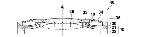
- FIG. 1 is a schematic cross-sectional view of an embodiment of a focusing mechanism of the present invention.
- FIG. 2 is a schematic cross-sectional view during driving of an embodiment of the focusing mechanism of the present invention.
- FIG. 3 is a schematic top view of the driving source of the focusing mechanism of the present invention.
- FIG. 4 is a schematic top view of the optical lens unit of the focusing mechanism of the present invention.
- FIG. 5 is a schematic cross-sectional view showing a process of manufacturing a driving source for the focusing mechanism of the present invention.
- FIG. 6 is a schematic cross-sectional view showing a manufacturing process of the optical lens unit of the focusing mechanism of the present invention.
- FIG. 7 is a schematic sectional view showing an imaging module using the focusing mechanism of the present invention.
- FIG. 1 is a schematic cross-sectional view of an embodiment of a focusing mechanism of the present invention.
- FIG. 2 is a schematic cross-sectional view during driving of an embodiment of the focusing mechanism of the
- FIG. 8 is a schematic top view showing a drive source of another embodiment of the focusing mechanism of the present invention.
- FIG. 9 is a schematic top view showing a state in which an optical lens is arranged on a drive source of another embodiment of the focusing mechanism of the present invention.
- FIG. 10 is an enlarged schematic view of the drive source showing the lengths of the actuators arranged in a spiral shape.
- FIG. 11 is a graph showing the voltage of the example and the displacement amount of the optical lens.
- FIG. 1 shows a schematic cross-sectional view of the focusing mechanism of the present invention in a state where no voltage is applied.
- FIG. 2 shows a schematic cross-sectional view of the focusing mechanism of the present invention when a voltage is applied.
- FIG. 3 shows a schematic top view of the drive source.
- FIG. 4 shows a schematic top view of the optical lens unit.
- the focusing mechanism 40 of the present invention includes a drive source 10 in which 32 cantilever piezoelectric actuators 21 (hereinafter simply referred to as actuators) are radially arranged on a ring-shaped support 22.
- actuators cantilever piezoelectric actuators 21
- the actuator 21 is in contact with the lens holding portion 33 at a surface 25 perpendicular to the optical axis direction of the optical lens at the driving tip 24 of the actuator 21, and the optical lens 36 is moved in the optical axis direction A of the optical lens 36 by driving the actuator 21. Move and focus.
- the actuator 21 warps to the upper surface side (upward on the paper surface) due to the unimorph effect. As a result, the optical lens 36 is lifted in the optical axis direction A via the protrusion 18. Since the optical lens 36 is supported by the elastic body 34, the optical lens 36 can move quickly without being constrained.
- the drive source 10 is made up of 32 rectangular actuators 21 arranged radially.
- the actuator 21 is arranged radially with the ring-shaped support body 22 as a common support body.
- the actuator 21 is provided with a protrusion 18 on a surface 25 perpendicular to the optical axis direction A of the optical lens at the driving tip 24.
- the protrusion 18 is in contact with the lens holding portion 33 of the optical lens unit 30. Since the protrusion 18 is provided, the actuator 21 and the lens holding portion 33 are in point contact with each other, so that it is possible to improve the decrease in the displacement due to friction.
- the protrusion 18 is further covered with a material having a static friction coefficient of 0.5 or less (not shown). Since the projection 18 is covered with a material having a static friction coefficient of 0.5 or less, the actuator 21 and the lens holding portion 33 are slippery when driven, and there is almost no structural constraint. In the conventional diaphragm or beam type structure, the displacement is greatly reduced because the actuator is strongly restrained, and the displacement necessary for focusing cannot be achieved. Thus, since the optical lens is supported by a material having a static friction coefficient of 0.5 or less and a low friction, a high displacement can be ideally realized.
- the projection part 18 does not need to be formed.
- the low friction material may be provided on the entire surface 25 or only the driving tip 24.
- the optical lens unit 30 is connected to the outer frame 35, the optical lens 36, the lens holding unit 33 that holds the optical lens 36 around the optical lens 36, and the lens holding unit 33. It consists of an elastic body that expands and contracts in the radial direction of the optical lens 36.
- the elastic body 34 is a bellows structure that is formed all around the optical lens 36 and expands and contracts in the radial direction of the optical lens.
- the optical lens unit 30 is in contact with the protrusion 18 of the drive source 10 on the back surface of the lens holding portion 33 as shown in FIG.
- the optical lens unit 30 is driven by the elastic body 34 so that the optical lens 36 and the lens holding portion 33 do not fall due to gravity or inertia force, or the optical axis of the optical lens 36 does not shift. It is suppressed to the 10 side.
- the elastic body 34 is made of, for example, a silicon nitride film having a bellows structure formed integrally with the lens holding portion 33 and the outer frame 35.
- the bellows structure using the microfabrication technique is used as the elastic body, but it is also possible to use a plurality of springs manufactured using, for example, an injection molding technique. In this case, it does not need to be formed around the entire periphery of the optical lens, and may have a structure in which a plurality of elastic bodies are arranged radially.
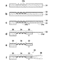
- FIG. 5 shows a schematic cross-sectional view of the manufacturing process of an embodiment of the drive source.
- a silicon substrate 11 is prepared. Since the thickness of the silicon substrate 11 serves as a support for a plurality of cantilever piezoelectric actuators, it is preferably, for example, 300 ⁇ m to 800 ⁇ m from the viewpoint of preventing the entire structure from being deformed by driving the actuator.
- the substrate is not limited to a silicon substrate, and examples of the substrate include glass, stainless steel, yttrium stabilized zirconia (YSZ), alumina, sapphire, and silicon carbide.
- thermal oxide films (silicon oxide) 12 and 13 are formed on the front and back surfaces of the silicon substrate 11.
- the thermal oxide films 12 and 13 serve as etching stoppers.
- the thickness of the thermal oxide film is preferably 0.5 ⁇ m to 3 ⁇ m from the viewpoint of the role of an etching stopper and the manufacturing cost.
- a polysilicon film 14 is formed on the surface of the thermal oxide film 13 on the side where the optical lens unit is disposed by a CVD (Chemical Vapor Deposition) method.
- the film thickness of the polysilicon film 14 is preferably 5 ⁇ m to 30 ⁇ m, for example, from the viewpoint of rigidity and displacement necessary for driving the lens.
- the main material of the actuator 21 is preferably an isotropic material such as polysilicon, amorphous silicon, and amorphous silicon carbide, avoiding crystalline silicon. Since crystalline silicon is an anisotropic material, when an inch lever type piezoelectric actuator having actuators arranged radially is manufactured, the rigidity of the actuator varies in the plane.
- an isotropic material such as polysilicon is preferably used as the main material of the actuator 21.
- the lower electrode 15, the ferroelectric thin film 16, and the upper electrode 17 are sequentially formed on the polysilicon film 14 by sputtering (see FIGS. 5d, 5e, and 5f).
- the ferroelectric thin film 16 is preferably one or more perovskite oxides represented by the following composition formula (1).
- M is composed of V, Nb, Ta, Sb, Cr, Mo, W, Mn, Mg, Sc, Co, Cu, In, Sn, Ga, Zn, Cd, Fe, Ni, Hf, and Al. It contains at least one element selected from the group.
- x, y, and z satisfy the relationships 0 ⁇ y ⁇ b, 0 ⁇ z ⁇ b, and 0 ⁇ b ⁇ yz.
- the perovskite oxide that can be represented by the composition formula (1) may contain Nb as M in the composition formula, and the Nb / (Zr + Ti + M) molar ratio may be 0.10 or more and 0.20 or less. 10 to 0.15 is more preferable.
- sputtering method As a preferable film forming method of the ferroelectric thin film 16, sputtering method, plasma CVD method, MOCVD method (metal organic vapor phase growth method, Metal Organic Chemical Vapor Deposition), firing quench quench method, annealing quench method, and spray quench quench And vapor phase growth methods such as the method.
- MOCVD method metal organic vapor phase growth method, Metal Organic Chemical Vapor Deposition
- firing quench quench method annealing quench method
- spray quench quench And vapor phase growth methods such as the method.
- the sputtering method is particularly preferable.
- the material of the lower electrode 15 and the upper electrode 17 is not particularly limited, Au, Pt, Ir, Ti , IrO 2, RuO 2, LaNiO 3, SrRuO 3, ITO ( indium tin oxide) (Indium Tin Oxide), TiN or the like Metal or metal oxide, and combinations thereof.
- the thickness of the lower electrode 15 and the upper electrode 17 is not particularly limited and is, for example, about 200 nm.
- the film thickness of the ferroelectric thin film 16 is not particularly limited, and is usually 1 ⁇ m or more, for example, 1 ⁇ m to 5 ⁇ m.
- the film thickness of the ferroelectric thin film 16 is preferably 3 ⁇ m or more.
- a protrusion 18 is formed in a region that becomes the driving tip of the actuator.
- the protrusion 18 is in contact with the lens holding portion 33 of the optical lens unit 30.
- the protrusion 18 can be formed, for example, by discharging a UV curable resin material with an inkjet for material deposition, and then curing the dropped droplet by UV irradiation.
- the UV curable resin material include a low-viscosity urethane acrylate resin.
- the surface of the protrusion 18 is preferably covered with a material having a static friction coefficient of 0.5 or less from the viewpoint of preventing a decrease in displacement due to friction with the lens holding portion 33.
- the protrusion itself may be made of a material having a static friction coefficient of 0.5 or less.
- Examples of materials having a static friction coefficient of 0.5 or less include fluorine resins such as Teflon (registered trademark, hereinafter omitted), graphite, molybdenum disulfide, DLC (Diamond-Like Carbon), polyethylene, polystyrene, and the like. Can be mentioned.
- the coefficient of static friction is a value measured by a measurement method based on ISO 8295.
- the resist 19 is protected from the surface of the actuator to the thermal oxide film 13.
- lithography for deep silicon etching is performed from the back surface, the thermal oxide film 12 is removed by wet etching, and the silicon substrate 11 is deep etched by Bosch dry etching.
- the thermal oxide film 13 becomes an etching stop layer (see FIGS. 5k and 5l).
- the thermal oxide film 13 exposed by vapor HF (hydrogen fluoride) etching is removed, and the protective resist 19 is removed by an asher.
- Teflon is sputtered on the surface.
- the thickness of the sputtered film is preferably 40 nm to 500 nm from the viewpoint of wear resistance and prevention of peeling due to residual stress.
- the length of the cantilever piezoelectric actuator means the length in the long side direction from the end of the support to the driving front end surface of the actuator in a region where the actuator 21 is not supported by the support 22. In the present embodiment, as shown in FIG. 5 m, it indicates the distance L 1 from the end portion 26 of the support 22 to the tip surface 23 of the actuator 21.
- each actuator it is preferable to design each actuator as described above.
- the arrangement shape of the cantilevers may be arranged so as to be radial from the center of the circle as in the present embodiment, or may be arranged spirally (in the case of Example 2 described later).
- the driving tips of the plurality of actuators only need to be arranged to form a circle.
- FIG. 6 shows a schematic cross-sectional view of the manufacturing process of the optical lens unit 30.
- a silicon substrate 31 is prepared, and a concavo-convex structure 31a is provided in a region where an elastic body is formed.
- the depth of the concave portion varies depending on the material to be used, but the viewpoint is to maximize the displacement of the actuator 21 and the optical lens is pressed against the driving source 10 so as not to drop due to gravity or inertia.
- the uneven period is preferably 1 ⁇ m to 100 ⁇ m, and preferably about 2 ⁇ m to 20 ⁇ m.
- the substrate glass, stainless steel, yttrium-stabilized zirconia, alumina, sapphire, silicon carbide, or the like can be used in addition to silicon. Further, the thickness of the silicon substrate 31 is preferably about 300 ⁇ m to 800 ⁇ m, for example.
- a silicon nitride film 32 is formed on the surface where the concavo-convex structure 31a is formed.
- This silicon nitride film 32 becomes an elastic body.
- the thickness of the silicon nitride film is preferably 0.1 ⁇ m to 2 ⁇ m and more preferably 0.2 ⁇ m to 1 ⁇ m from the viewpoint of providing strength and elasticity.
- the region 31b where the elastic body 34 is formed and the region 31c where the optical lens 36 is disposed on the back side of the silicon substrate 31 are removed by dry etching in two stages (see FIGS. 6c and 6d).
- the silicon nitride film 32 serves as a stopper.
- a material of the elastic body a film containing at least one material of silicon oxide, Al, Ni, Au, and Cu in addition to silicon nitride can be used.
- the silicon nitride film 32 in the portion 31d where the optical lens is disposed is removed, and the lens holding portion 33, the elastic body 34, and the outer frame 35 are formed.
- the separately prepared optical lens 36 is fixed to the lens holding portion 33 with an adhesive.
- the adhesive it is preferable to use an epoxy die bond resin, a fluorine die bond resin, a silicon die bond resin or the like that does not affect the function of the optical lens.
- the lens holding portion 33 of the optical lens unit 30 is disposed on the projection 18 of the drive source 10 manufactured as described above, and the outer frame 35 of the optical lens unit and the actuator 21 are bonded with an adhesive.
- the adhesive it is preferable to use an epoxy die bond resin.
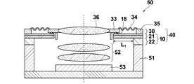
- FIG. 7 is a schematic sectional view showing an embodiment of the imaging module.
- the imaging module 50 according to the present embodiment includes a focusing mechanism 40 according to the present invention that includes a driving source 10 and an optical lens unit 30, and a fixed lens group 52 and an imaging element 53 disposed therein. It is fixed on the casing 51 with an adhesive.
- the optical lens 36 of the optical lens unit 30 moves in the optical axis direction A by the drive of the cantilever piezoelectric actuator 21 and functions as a focusing lens.
- the optical lens 36 serving as a focusing lens and the fixed lens group 52 perform focusing on an object to be imaged at an arbitrary distance to form an optical image on the image sensor 53.
- the imaging module having the focusing mechanism of the present invention uses a cantilever piezoelectric actuator made of a thin film, it is possible to achieve downsizing and low power consumption. Furthermore, since the drive source and the optical lens are not fixed and are in point contact, and the optical lens is supported by an elastic body, the optical lens can quickly move in the optical axis direction. As described above, the imaging module including the focusing mechanism of the present invention can be driven at high speed and with low power consumption without degrading the quality of image quality.
- the driving source of the focusing mechanism has been described in which the actuators are arranged radially.
- the driving source may be one in which the actuators are arranged in a spiral shape.
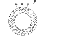
- FIG. 8 shows a schematic top view of the drive source.
- FIG. 9 is a schematic top view showing a state where the optical lens of the drive source is arranged.
- the drive source 60 is formed by arranging 18 actuators 61 having the same shape and the same length on a ring-shaped support body 62 in a spiral shape.
- the actuator 61 has a shape in which the end surface in the major axis direction of the actuator 61 forms an arc.
- a protrusion 68 is provided on a surface perpendicular to the optical axis direction of the optical lens at the driving tip of the actuator 61.
- the optical lens 36 is disposed so that the protrusion 68 is in contact with the lens holding portion 33 of the optical lens unit 30 (see FIG. 9).
- the holding portion, the elastic body, and the outer frame are omitted.
- the lengths of the actuators 61 arranged in a spiral manner as described above are the center L of the tip surface 63 of the actuator 61 and the center of the end where the actuator 61 contacts the support body 62, as shown in FIG. to the the length defined straight line L 2 connecting the between the M.
- a piezoelectric element having a long length can be formed in a narrow region, and without increasing the size of the entire focusing mechanism (or without reducing the size of the optical lens). A high amount of displacement can be obtained.
- Example 1 The driving source and the optical lens unit were manufactured under the following conditions by the manufacturing method described in the embodiment, and the focusing mechanism was manufactured by bonding the driving source and the optical lens unit with an adhesive.
- Silicon substrate diameter 150mm, thickness 350 ⁇ m
- Thermal oxide film 0.5 ⁇ m thickness
- Polysilicon film 10 ⁇ m thick
- Lower electrode Ti (thickness 20 nm) / Ir (thickness 100 nm)
- Upper electrode Ir (thickness 100 nm)
- Piezoelectric film lead zirconate titanate (PZT with 12% Nb added to the B site), thickness 3 ⁇ m
- Cantilever type piezoelectric actuator length L 1 1 mm.
- Protrusion material Low viscosity urethane acrylate UV curable resin
- Protrusion material Teflon (Static friction coefficient 0.1)
- Silicon substrate diameter 150mm, thickness 350 ⁇ m Silicon nitride film: 1 ⁇ m
- Optical lens size Diameter 2.5mm
- Example 2 The focusing mechanism of the second embodiment is the same as that of the first embodiment except that the drive source 60 is used.
- the length L 2 of the cantilevered piezoelectric actuator 61 of the driving source of Example 2 was 2 mm.
- the other drive source configurations are the same as those in the first embodiment.
- Example 1 Lid displacement measurement method- At each applied voltage, the difference in height between the center of the lens 36 and the outer frame 35 was statically measured by a white interference shape measuring device, and the value at a voltage of 0 V was set to zero.
- the measurement results of Example 1 and Example 2 are shown in FIG.
- the focusing mechanism of the present invention obtained a displacement of 50 to 100 ⁇ m at a voltage of 20 to 30V.
- a displacement amount approximately twice as large as that at an applied voltage of 30 V was obtained.
Landscapes
- Physics & Mathematics (AREA)
- General Physics & Mathematics (AREA)
- Optics & Photonics (AREA)
- Lens Barrels (AREA)
- Automatic Focus Adjustment (AREA)
- General Electrical Machinery Utilizing Piezoelectricity, Electrostriction Or Magnetostriction (AREA)
Abstract
Le problème décrit par la présente invention est de produire un mécanisme de mise au point et un module d'imagerie pouvant déplacer une lentille optique sur une grande plage de déplacement à l'aide d'une structure simple, et pouvant être entraînés à grande vitesse avec une faible consommation d'énergie. La solution selon l'invention porte sur le mécanisme de mise au point comprenant : une source d'entraînement (10) comprenant au moins trois actionneurs piézoélectriques en porte-à-faux disposés radialement (21); et une unité de lentille optique (30) comprenant un cadre externe (35), une lentille optique (36), un support de lentille (33) pour maintenir la lentille optique (36) sur sa périphérie, et un corps élastique (34) qui raccorde le support de lentille (33) au cadre externe (35) et qui est flexible le long de la direction radiale de la lentille optique (36). L'actionneur piézoélectrique en porte-à-faux (21) est en contact avec le support de lentille (33) par une surface (25) perpendiculaire à une direction d'axe optique A de la lentille optique (36) située à proximité d'une extrémité d'entraînement (24) de l'actionneur piézoélectrique en porte-à-faux (21). L'actionneur piézoélectrique en porte-à-faux (21) est entraîné, lequel à son tour déplace la lentille optique (36) le long de la direction d'axe optique A de celle-ci (36) de façon à effectuer une mise au point.
Priority Applications (2)
| Application Number | Priority Date | Filing Date | Title |
|---|---|---|---|
| JP2018509127A JP6537707B2 (ja) | 2016-03-29 | 2017-03-22 | フォーカシング機構および撮像モジュール |
| US16/116,422 US10921548B2 (en) | 2016-03-29 | 2018-08-29 | Focusing mechanism and imaging module |
Applications Claiming Priority (2)
| Application Number | Priority Date | Filing Date | Title |
|---|---|---|---|
| JP2016-065306 | 2016-03-29 | ||
| JP2016065306 | 2016-03-29 |
Related Child Applications (1)
| Application Number | Title | Priority Date | Filing Date |
|---|---|---|---|
| US16/116,422 Continuation US10921548B2 (en) | 2016-03-29 | 2018-08-29 | Focusing mechanism and imaging module |
Publications (1)
| Publication Number | Publication Date |
|---|---|
| WO2017170046A1 true WO2017170046A1 (fr) | 2017-10-05 |
Family
ID=59965363
Family Applications (1)
| Application Number | Title | Priority Date | Filing Date |
|---|---|---|---|
| PCT/JP2017/011477 Ceased WO2017170046A1 (fr) | 2016-03-29 | 2017-03-22 | Mécanisme de mise au point et module d'imagerie |
Country Status (3)
| Country | Link |
|---|---|
| US (1) | US10921548B2 (fr) |
| JP (1) | JP6537707B2 (fr) |
| WO (1) | WO2017170046A1 (fr) |
Cited By (2)
| Publication number | Priority date | Publication date | Assignee | Title |
|---|---|---|---|---|
| WO2019181455A1 (fr) * | 2018-04-12 | 2019-09-26 | 国立研究開発法人物質・材料研究機構 | Mécanisme de commande de mise au point automatique faisant appel à un réseau d'actionneurs à film mince en alliage à mémoire de forme |
| CN110365247A (zh) * | 2019-06-28 | 2019-10-22 | 西安工程大学 | 一种基于液压放大机构的压电驱动器及其驱动方法 |
Families Citing this family (6)
| Publication number | Priority date | Publication date | Assignee | Title |
|---|---|---|---|---|
| CN112825542B (zh) * | 2019-11-20 | 2022-10-14 | 中芯集成电路(宁波)有限公司 | 一种成像模组 |
| CN112825321B (zh) * | 2019-11-21 | 2022-03-22 | 中芯集成电路(宁波)有限公司 | 一种成像模组的制造方法 |
| CN113131782B (zh) * | 2019-12-31 | 2024-07-26 | 中芯集成电路(宁波)有限公司 | 一种压电驱动器及其制造方法和成像模组 |
| CN111399164B (zh) * | 2020-03-27 | 2021-08-31 | 睿恩光电有限责任公司 | 压电片式对焦装置、相机装置及电子设备 |
| CN111856694B (zh) * | 2020-08-17 | 2024-11-26 | 精拓丽音科技(北京)有限公司 | 一种可变焦镜头组件及应用其的电子设备 |
| CN118091920A (zh) * | 2024-03-29 | 2024-05-28 | 苏州大学 | 一种大景深样本调焦平台及其显微镜 |
Citations (3)
| Publication number | Priority date | Publication date | Assignee | Title |
|---|---|---|---|---|
| JP2004001209A (ja) * | 2002-04-30 | 2004-01-08 | Xerox Corp | 微小電気機械システム、及び、静電力を用いて可動電極を移動させる方法 |
| WO2009060575A1 (fr) * | 2007-11-05 | 2009-05-14 | Panasonic Corporation | Dispositif d'entraînement de support de lentille et dispositif d'imagerie utilisant un actionneur polymère à entraînement planaire |
| JP2012163415A (ja) * | 2011-02-04 | 2012-08-30 | Seiko Epson Corp | 加速度センサー及びその製造方法 |
Family Cites Families (5)
| Publication number | Priority date | Publication date | Assignee | Title |
|---|---|---|---|---|
| NO326372B1 (no) | 2006-09-21 | 2008-11-17 | Polight As | Polymerlinse |
| JP5158720B2 (ja) | 2009-03-11 | 2013-03-06 | 富士フイルム株式会社 | 光学モジュールおよびその製造方法、並びに撮像装置 |
| JP5430413B2 (ja) | 2010-01-07 | 2014-02-26 | 富士フイルム株式会社 | 可変焦点レンズ及びその駆動方法 |
| JP2013068875A (ja) | 2011-09-26 | 2013-04-18 | Panasonic Corp | 可変焦点レンズおよびその製造方法ならびに可変焦点レンズを備えた撮像装置 |
| US8711495B2 (en) | 2012-10-01 | 2014-04-29 | Apple Inc. | MEMS autofocus actuator |
-
2017
- 2017-03-22 WO PCT/JP2017/011477 patent/WO2017170046A1/fr not_active Ceased
- 2017-03-22 JP JP2018509127A patent/JP6537707B2/ja not_active Expired - Fee Related
-
2018
- 2018-08-29 US US16/116,422 patent/US10921548B2/en active Active
Patent Citations (3)
| Publication number | Priority date | Publication date | Assignee | Title |
|---|---|---|---|---|
| JP2004001209A (ja) * | 2002-04-30 | 2004-01-08 | Xerox Corp | 微小電気機械システム、及び、静電力を用いて可動電極を移動させる方法 |
| WO2009060575A1 (fr) * | 2007-11-05 | 2009-05-14 | Panasonic Corporation | Dispositif d'entraînement de support de lentille et dispositif d'imagerie utilisant un actionneur polymère à entraînement planaire |
| JP2012163415A (ja) * | 2011-02-04 | 2012-08-30 | Seiko Epson Corp | 加速度センサー及びその製造方法 |
Cited By (3)
| Publication number | Priority date | Publication date | Assignee | Title |
|---|---|---|---|---|
| WO2019181455A1 (fr) * | 2018-04-12 | 2019-09-26 | 国立研究開発法人物質・材料研究機構 | Mécanisme de commande de mise au point automatique faisant appel à un réseau d'actionneurs à film mince en alliage à mémoire de forme |
| JPWO2019181455A1 (ja) * | 2018-04-12 | 2021-03-11 | 国立研究開発法人物質・材料研究機構 | 形状記憶合金薄膜アクチュエータアレイによるオートフォーカス駆動機構 |
| CN110365247A (zh) * | 2019-06-28 | 2019-10-22 | 西安工程大学 | 一种基于液压放大机构的压电驱动器及其驱动方法 |
Also Published As
| Publication number | Publication date |
|---|---|
| JPWO2017170046A1 (ja) | 2018-09-13 |
| US20180364449A1 (en) | 2018-12-20 |
| US10921548B2 (en) | 2021-02-16 |
| JP6537707B2 (ja) | 2019-07-03 |
Similar Documents
| Publication | Publication Date | Title |
|---|---|---|
| JP6537707B2 (ja) | フォーカシング機構および撮像モジュール | |
| US8385013B2 (en) | Optical module, method for production thereof, and imaging apparatus | |
| JP6560311B2 (ja) | 圧電作動変形可能メンブレンを有する光学デバイス | |
| JP6889867B2 (ja) | 連続冠状部形成圧電作動変形可能メンブレンを有する光学デバイス | |
| US8879132B2 (en) | Mirror driving apparatus, method of driving same and method of manufacturing same | |
| JP5224617B2 (ja) | 圧電アクチュエータ、可変容量コンデンサ及び光偏向素子 | |
| US7170665B2 (en) | Optical unit provided with an actuator | |
| US9030721B2 (en) | Mirror driving device and method of controlling the device | |
| US8649079B2 (en) | Mirror driving device and mirror driving method | |
| CN111983801B (zh) | 用于补偿不期望的运动的压电mems致动器及其制造工艺 | |
| EP1255307A1 (fr) | Element piézoélectrique, actionneur, et tête d'impression à jet d'encre | |
| US20070024715A1 (en) | Actuator and micromotion mechanism having such actuator and camera module having such micromotion mechanism | |
| CN108249388B (zh) | 可在平面中移动的压电式微机电致动器设备 | |
| JP6018926B2 (ja) | マイクロミラーデバイス及びその製造方法 | |
| CN113728263A (zh) | 微镜器件 | |
| JP2025019739A (ja) | アクチュエータ、液体吐出ヘッド、液体吐出装置、ウェアラブル端末装置、アイトラッキング装置およびその製造方法。 | |
| Goto et al. | Microfocusing optical device using piezoelectric thin-film actuator | |
| Phelps et al. | Single-layer thin-film lithium niobate out-of-plane actuators | |
| Yang et al. | Concept, modeling, and fabrication techniques for large-stroke piezoelectric unimorph deformable mirrors | |
| JP2006003814A (ja) | 形状可変ミラー素子 | |
| JP2007158167A (ja) | 超音波モータ素子およびその製造方法 | |
| JP2002228947A (ja) | 可変形状鏡 | |
| JP2005195837A (ja) | 形状可変ミラー素子及び形状可変ミラー素子の製造方法 |
Legal Events
| Date | Code | Title | Description |
|---|---|---|---|
| ENP | Entry into the national phase |
Ref document number: 2018509127 Country of ref document: JP Kind code of ref document: A |
|
| NENP | Non-entry into the national phase |
Ref country code: DE |
|
| 121 | Ep: the epo has been informed by wipo that ep was designated in this application |
Ref document number: 17774587 Country of ref document: EP Kind code of ref document: A1 |
|
| 122 | Ep: pct application non-entry in european phase |
Ref document number: 17774587 Country of ref document: EP Kind code of ref document: A1 |