WO2017170870A1 - 配線体、配線基板、及びタッチセンサ - Google Patents
配線体、配線基板、及びタッチセンサ Download PDFInfo
- Publication number
- WO2017170870A1 WO2017170870A1 PCT/JP2017/013269 JP2017013269W WO2017170870A1 WO 2017170870 A1 WO2017170870 A1 WO 2017170870A1 JP 2017013269 W JP2017013269 W JP 2017013269W WO 2017170870 A1 WO2017170870 A1 WO 2017170870A1
- Authority
- WO
- WIPO (PCT)
- Prior art keywords
- conductor portion
- conductor
- resin
- wiring body
- face
- Prior art date
- Legal status (The legal status is an assumption and is not a legal conclusion. Google has not performed a legal analysis and makes no representation as to the accuracy of the status listed.)
- Ceased
Links
Images



Classifications
-
- G—PHYSICS
- G06—COMPUTING OR CALCULATING; COUNTING
- G06F—ELECTRIC DIGITAL DATA PROCESSING
- G06F3/00—Input arrangements for transferring data to be processed into a form capable of being handled by the computer; Output arrangements for transferring data from processing unit to output unit, e.g. interface arrangements
- G06F3/01—Input arrangements or combined input and output arrangements for interaction between user and computer
- G06F3/03—Arrangements for converting the position or the displacement of a member into a coded form
- G06F3/041—Digitisers, e.g. for touch screens or touch pads, characterised by the transducing means
- G06F3/044—Digitisers, e.g. for touch screens or touch pads, characterised by the transducing means by capacitive means
- G06F3/0445—Digitisers, e.g. for touch screens or touch pads, characterised by the transducing means by capacitive means using two or more layers of sensing electrodes, e.g. using two layers of electrodes separated by a dielectric layer
-
- G—PHYSICS
- G06—COMPUTING OR CALCULATING; COUNTING
- G06F—ELECTRIC DIGITAL DATA PROCESSING
- G06F3/00—Input arrangements for transferring data to be processed into a form capable of being handled by the computer; Output arrangements for transferring data from processing unit to output unit, e.g. interface arrangements
- G06F3/01—Input arrangements or combined input and output arrangements for interaction between user and computer
- G06F3/03—Arrangements for converting the position or the displacement of a member into a coded form
- G06F3/041—Digitisers, e.g. for touch screens or touch pads, characterised by the transducing means
- G06F3/044—Digitisers, e.g. for touch screens or touch pads, characterised by the transducing means by capacitive means
- G06F3/0446—Digitisers, e.g. for touch screens or touch pads, characterised by the transducing means by capacitive means using a grid-like structure of electrodes in at least two directions, e.g. using row and column electrodes
-
- G—PHYSICS
- G06—COMPUTING OR CALCULATING; COUNTING
- G06F—ELECTRIC DIGITAL DATA PROCESSING
- G06F2203/00—Indexing scheme relating to G06F3/00 - G06F3/048
- G06F2203/041—Indexing scheme relating to G06F3/041 - G06F3/045
- G06F2203/04103—Manufacturing, i.e. details related to manufacturing processes specially suited for touch sensitive devices
-
- G—PHYSICS
- G06—COMPUTING OR CALCULATING; COUNTING
- G06F—ELECTRIC DIGITAL DATA PROCESSING
- G06F2203/00—Indexing scheme relating to G06F3/00 - G06F3/048
- G06F2203/041—Indexing scheme relating to G06F3/041 - G06F3/045
- G06F2203/04112—Electrode mesh in capacitive digitiser: electrode for touch sensing is formed of a mesh of very fine, normally metallic, interconnected lines that are almost invisible to see. This provides a quite large but transparent electrode surface, without need for ITO or similar transparent conductive material
Definitions
- the present invention relates to a wiring body, a wiring board, and a touch sensor.
- a wiring body for the designated countries that are allowed to be incorporated by reference, the contents described in Japanese Patent Application No. 2016-0667614 filed in Japan on March 30, 2016 are incorporated herein by reference. Part of the description.
- a touch panel in which a two-layer electrode pattern including a plurality of grids composed of fine metal wires is arranged so as to intersect to form a combination pattern composed of a plurality of small grids. (For example, refer to Patent Document 1).
- a conductive wiring pattern formed by transferring the conductive material to a substrate to be transferred using an offset printing method and performing a subsequent heating step is known (for example, Patent Document 2).
- the fine metal wire constituting the electrode pattern of the touch panel of Patent Document 1 has a shape with a skirt as in Patent Document 2, the fine metal wire is easily visible, the combination pattern is glaring, etc. There is a problem that visibility is lowered.
- the problem to be solved by the present invention is to provide a wiring body, a wiring board, and a touch sensor that can improve visibility.
- a wiring body includes a first resin portion and a linear first conductor portion provided on the first resin portion, and the first conductor portion includes:
- the wiring body has a first end face located at a tip in a first extending direction of the first conductor portion and satisfies the following expression (1).
- W 1 / T 1 ⁇ 1 (1)
- W 1 is a first length obtained by projecting the first end face onto a plane parallel to the first extending direction
- T 1 is the first conductor portion. It is height.
- the first conductor portion includes a contact surface in contact with the first resin portion, a top surface located on the opposite side of the contact surface, and between the contact surface and the top surface. And a side surface connected to the first end surface, and the first end surface may have an arc portion connected to the side surface.
- W 1 W 2 (2)
- W 2 is a second length obtained by projecting the side surface onto a plane parallel to the width direction of the first conductor portion.
- the first conductor portion may have a protruding portion that is formed along a peripheral edge of the top surface and protrudes toward a side away from the first resin portion.
- the height of the first conductor portion may be 500 nm to 10 ⁇ m.
- the first resin portion is provided corresponding to a flat portion formed in a layer shape and the first conductor portion, and the first conductor portion side from the flat portion.
- a convex portion projecting toward the first surface, and the convex portion has a third end surface located at a tip in the first extending direction, and the first end surface and the third end surface are Are connected continuously, and may satisfy the following expression (3).
- W 5 / T 2 ⁇ 1 (3)
- W 5 is the sum of the first length and the length of the third end face projected onto a plane parallel to the first extending direction
- T 2 is the first length.
- 1 is the sum of the height of the conductor portion and the height of the convex portion.
- a second resin portion provided so as to cover the first conductor portion and a height substantially the same as the first conductor portion provided on the second resin portion.
- a linear second conductor portion having a thickness, and the second conductor portion has a second end face located at a tip in the second extending direction of the second conductor portion.
- the first and second conductor portions are located on the same imaginary straight line in a transmission plan view, and the first and second end faces are arranged to face each other in the transmission plan view. And may satisfy the following expressions (4) and (5).
- W 3 is of a length obtained by projecting the distance between the first and second end faces in the third direction parallel to the extending plane of the imaginary straight line shortest W 4 is the longest fourth length among the lengths obtained by projecting the distance between the first and second end faces onto a plane parallel to the third extending direction. .
- a wiring board according to the present invention is a wiring board including the wiring body and a support body that supports the wiring body.
- a touch sensor according to the present invention is a touch sensor including the wiring board.
- the tip of the first conductor portion does not have a skirted shape. For this reason, since it becomes difficult to visually recognize a 1st conductor part, the visibility of a wiring body can be improved.
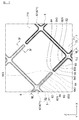
- FIG. 1 is a plan view showing a touch sensor according to an embodiment of the present invention.
- FIG. 2 is an exploded perspective view showing a wiring board according to an embodiment of the present invention.
- FIG. 3 is a partially enlarged view of part III in FIG. 4 is a cross-sectional view taken along line IV-IV in FIG.
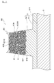
- FIG. 5 is a cross-sectional view for explaining the first conductor portion according to the embodiment of the present invention.
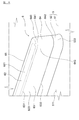
- FIG. 6 is a perspective view of the front end of the first conductor portion according to the embodiment of the present invention as viewed from above.
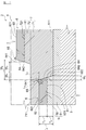
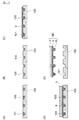
- 7 is a cross-sectional view taken along line VII-VII in FIG. 8A to 8E are cross-sectional views (No. 1) for explaining the method of manufacturing the wiring body according to the embodiment of the invention.
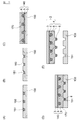
- FIGS. 9A to 9E are cross-sectional views (part 2) for explaining the method of manufacturing the wiring body according to the embodiment of the invention.
- FIG. 1 is a plan view showing a touch sensor according to one embodiment of the present invention
- FIG. 2 is an exploded perspective view showing a wiring board according to one embodiment of the present invention
- FIG. 3 is a partially enlarged view of a portion III in FIG. 4 is a cross-sectional view taken along line IV-IV of FIG. 3
- FIG. 5 is a cross-sectional view for explaining a first conductor portion according to an embodiment of the present invention
- FIG. FIG. 7 is a cross-sectional view taken along the line VII-VII in FIG. 3.
- the touch sensor 1 including the wiring board 2 of the present embodiment is a projected capacitive touch panel sensor.
- the touch position is set in combination with a display device (not shown) or the like. It is used as an input device having a detection function.
- the display device is not particularly limited, and a liquid crystal display, an organic EL display, electronic paper, or the like can be used.
- a detection electrode and a drive electrode are arranged so as to overlap with an image displayed on the display device, and between the two electrodes 67 and 87.
- a predetermined voltage is periodically applied from an external circuit (not shown).
- a touch sensor 1 for example, when an operator's finger (external conductor) approaches the touch sensor 1, a capacitor (electrical capacity) is formed between the external conductor and the touch sensor 1, and between the two electrodes. The electrical state of the changes.
- the touch sensor 1 can detect the operation position of the operator based on an electrical change between the two electrodes.
- the “touch sensor 1” in the present embodiment corresponds to an example of the “touch sensor” in the present invention
- the “wiring board 2” in the present embodiment corresponds to an example of the “wiring board” in the present invention.
- the wiring board 2 includes a base material 3 and a wiring body 4 as shown in FIGS.
- the wiring board 2 of the present embodiment is configured to have transparency (translucency) as a whole in order to ensure the visibility of the display device.
- the base material 3 is a transparent plate-like base material that transmits visible light and supports the wiring body 4.
- the material constituting the substrate 3 includes polyethylene terephthalate (PET), polyethylene naphthalate (PEN), polyimide resin (PI), polyetherimide resin (PEI), polycarbonate (PC), polyether ether ketone (PEEK). Examples thereof include liquid crystal polymer (LCP), cycloolefin polymer (COP), silicone resin (SI), acrylic resin, phenol resin, epoxy resin, green sheet, and glass.
- An easy-adhesion layer and an optical adjustment layer may be formed on the substrate 3.
- the “base 3” in the present embodiment corresponds to an example of the “support” in the present invention.
- the wiring body 4 includes a first resin portion 5, a first conductor portion 6, a second resin portion 7, and a second conductor portion 8.
- the first resin portion 5, the first conductor portion 6, the second resin portion 7, and the second conductor portion 8 are sequentially laminated from the base material 3 side.
- the “wiring body 4” in the present embodiment corresponds to an example of the “wiring body” in the present invention
- the “first resin portion 5” in the present embodiment corresponds to an example of the “first resin portion” in the present invention.
- first conductor portion 6 in the present embodiment corresponds to an example of the “first conductor portion” in the present invention
- the “second resin portion 7” in the present embodiment is the “second conductor portion” in the present invention
- the “second conductor portion” in the present embodiment corresponds to an example of the “second conductor portion” in the present invention.
- the 1st resin part 5 is provided in order to hold
- an insulating material such as a UV curable resin, a thermosetting resin, a thermoplastic resin, or a green sheet.
- the first resin part 5 has a first flat part 51 and a first convex part 52 as shown in FIG.
- the first flat portion 51 is a portion formed in a layer shape in the first resin portion 5.
- the first upper surface 511 of the first flat portion 51 is substantially flat.
- the thickness of the first flat part 51 is preferably 5 ⁇ m to 100 ⁇ m, for example.
- the first convex portion 52 is formed integrally with the first flat portion 51 on the first flat portion 51.
- the first convex portion 52 is provided corresponding to the first conductor portion 6 and supports the first conductor portion 6.
- the first convex portion 52 protrudes from the first flat portion 51 toward the first conductor portion 6 in the cross section in the width direction of the first conductor portion 6.
- the height T 3 of the first convex portion 52 is preferably 100 nm to 10 ⁇ m, and more preferably 500 nm to 5 ⁇ m.
- the width W 6 (maximum width) of the first convex portion 52 is preferably 50 ⁇ m or less.
- the first convex portion 52 is linearly formed along the extending direction of the first conductor portion 6 (hereinafter, also referred to as “first extending direction”).
- a convex end surface 522 is formed at the tip of the first convex portion 52 in the first extending direction. In the cross section along the first extending direction, the convex end surface 522 is inclined so as to protrude to the outside of the first convex portion 52 as it approaches the first flat portion 51.
- the “convex end surface 522” in the present embodiment corresponds to an example of a “third end surface” in the present invention.
- the 1st convex part 52 has the 1st resin part contact surface 521 which contacts the 1st conductor part 6 (specifically 1st conductor part contact surface 61 (after-mentioned)).
- the first resin portion contact surface 521 has an uneven shape that is complementary to the first conductor portion contact surface 61 having an uneven shape.
- the first resin portion contact surface 521 and the first conductor portion contact surface 61 are complementary to each other even in the first extending direction cross section of the first conductor portion 6. It has an uneven shape. 4 and 7, the concave and convex shapes of the first resin portion contact surface 521 and the first conductor portion contact surface 61 are exaggerated for easy understanding of the wiring body 4 of the present embodiment. .
- cross section in the extending direction of the conductor portion refers to a cross section of the conductor portion when cut on a virtual straight line that passes through the center of the conductor portion and extends in the extending direction in plan view.
- the “cross section in the width direction of the conductor portion” refers to a cross section of the conductor portion when cut on a virtual straight line extending in a direction orthogonal to the extending direction of the conductor portion in plan view.
- a plurality of first conductor portions 6 are provided on the first resin portion 5, and a first conductor pattern 66 is configured by the plurality of first conductor portions 6.
- the first conductor pattern 66 has a plurality of first electrodes 67, a plurality of first lead wires 68, and a plurality of first terminals 69.
- the first electrode 67 is configured by a plurality of first conductor portions 6 in a mesh shape.
- the first electrode 67 includes a plurality of rhombus-shaped first wide portions 671 and first connecting portions 672 that connect the first wide portions 671 to each other.
- the plurality of first wide portions 671 are arranged at substantially equal intervals along the X direction, and the corners of the adjacent first wide portions 671 are connected to each other by the first connecting portion 672. Is connected.
- the first wide portion 671 is illustrated with four straight sides for easy understanding of the first electrode 67, but each side of the actual first wide portion 671 is illustrated.
- the plurality of first conductor portions 6 have a comb-teeth shape with protruding ends. Note that the shape of the first wide portion 671 is not particularly limited to a rhombus shape.
- the plurality of first electrodes 67 are juxtaposed in the Y direction in the figure.
- a first lead wire 68 is connected to one end in the longitudinal direction of each first electrode 67.
- Each first lead-out line 68 extends from one end in the longitudinal direction of each first electrode 67 to the vicinity of the outer edge of the wiring body 4.
- a first terminal 69 is provided at the other end of each first lead-out wiring 68. The first terminal 69 is electrically connected to an external circuit (not shown).
- each mesh constituting the mesh shape of the first electrode 67 is not particularly limited.
- it may be a triangle such as a regular triangle, an isosceles triangle, a right triangle, or a quadrangle such as a parallelogram or a trapezoid.
- the mesh shape may be an n-gon such as a hexagon, an octagon, a dodecagon, or an icosahedron, a circle, an ellipse, or a star.
- a geometric pattern obtained by repeating various graphic units can be used as the shape of each mesh of the first electrode 67.
- the first lead wiring 68 and the first terminal 69 may have a mesh shape like the first electrode 67.
- the first conductor portion 6 of this embodiment will be described in detail.
- the first conductor portion 6 has a straight shape and is formed at a substantially constant height in the first extending direction.
- the mesh shape described above is formed by intersecting the plurality of first conductor portions 6 with each other.
- the first conductor portion 6 may have a curved shape, a horseshoe shape, a zigzag line shape, or the like as long as it extends linearly. Further, the width of the first conductor portion 6 may change along the first extending direction.
- the width (maximum width) of the first conductor portion 6 is preferably 50 nm to 1000 ⁇ m, more preferably 500 nm to 150 ⁇ m, still more preferably 1 ⁇ m to 10 ⁇ m, and 1 ⁇ m to 5 ⁇ m. Even more preferably. Further, the height T 1 of the first conductor portion 6 is preferably 50 nm to 3000 ⁇ m, more preferably 500 nm to 450 ⁇ m, and further preferably 500 nm to 10 ⁇ m. The height T 1 of the first conductor portion 6 is larger than the height T 3 of the first convex portion 52.
- the aspect ratio of the first conductor portion 6 (ratio of the width of the first conductor portion 6 to the height of the first conductor portion 6) is 1 from the viewpoint of achieving both conductivity and visibility. Is preferably larger.
- the height of the first conductor portion 6 is a distance between the first conductor portion contact surface 61 (average surface) and the first conductor portion top surface 62 (described later) along the Z direction.
- the first conductor portion 6 is composed of a binder resin and conductive particles (conductive powder) dispersed in the binder resin.
- Conductive particles include silver, copper, nickel, tin, bismuth, zinc, indium, palladium and other metal materials, graphite, carbon black (furnace black, acetylene black, ketjen black), carbon nanotubes, carbon nanofibers, etc. Can be mentioned. In addition, it may replace with electroconductive particle and may use the metal salt which is a salt of the above-mentioned metal material.
- the conductive particles contained in the first conductor part 6 may be, for example, a particle diameter ⁇ of 0.5 ⁇ m or more and 2 ⁇ m or less (0.5 ⁇ m ⁇ ⁇ ⁇ 2 ⁇ m) depending on the width of the first conductor part 6 to be formed. Conductive particles having can be used. In addition, from the viewpoint of stabilizing the electric resistance value in the first conductor portion 6, it is preferable to use conductive particles having an average particle diameter ⁇ of not more than half the width of the first conductor portion 6 to be formed. Further, as the conductive particles, it is preferable to use particles having a specific surface area measured by the BET method of 20 m 2 / g or more.
- the first conductor part 6 When a relatively small electrical resistance value of a certain value or less is required as the first conductor part 6, it is preferable to use a metal material as the conductive particles, but as the first conductor part 6, a relatively large value of a certain value or more. When the electrical resistance value is allowed, a carbon-based material can be used as the conductive particles. In addition, it is preferable to use a carbon-based material as the conductive particles from the viewpoint of improving the haze and total light reflectance of the mesh film.
- the first conductor portion 6 of the first electrode 67 is configured.
- the conductive material to be used it is possible to use silver, copper, nickel metal materials, and the above-described carbon-based materials, which are excellent in conductivity but opaque, such as opaque metal materials and opaque carbon-based materials.
- binder resin examples include acrylic resin, polyester resin, epoxy resin, vinyl resin, urethane resin, phenol resin, polyimide resin, silicone resin, and fluorine resin.
- the first conductor portion 6 is formed by applying and hardening a conductive paste.
- the conductive paste include a conductive paste configured by mixing conductive particles, a binder resin, water or a solvent, and various additives.
- the solvent contained in the conductive paste include ⁇ -terpineol, butyl carbitol acetate, butyl carbitol, 1-decanol, butyl cellosolve, diethylene glycol monoethyl ether acetate, and tetradecane.
- the first conductor portion 6 has a first conductor portion contact surface 61, a first conductor portion top surface 62, and a first conductor portion. It has a side surface 63, a first conductor portion end surface 64, and a first protrusion 65.
- the “first conductor portion contact surface 61” in the present embodiment corresponds to an example of the “contact surface” in the present invention
- the “first conductor portion top surface 62” in the present embodiment is the “top surface” in the present invention.
- the “first conductor end face 64” in the present embodiment corresponds to an example of the “first end face” of the present invention
- the “first protrusion 65” in the present embodiment corresponds to the present invention. Corresponds to an example of the “projection” in FIG.
- the first conductor portion contact surface 61 is a surface that is in contact with the first resin portion contact surface 521 and extends parallel to the first extending direction. is doing.
- the first conductor contact surface 61 has an uneven shape. The uneven shape is formed based on the surface roughness of the first conductor portion contact surface 61. The surface roughness of the first conductor portion contact surface 61 will be described in detail later.
- the first conductor portion top surface 62 is a surface opposite to the first conductor portion contact surface 61 in the first conductor portion 6, and extends in the first extending direction. It extends parallel to it.
- the first conductor portion top surface 62 in the present embodiment includes a linear first top surface flat portion 621.
- the width of the first top flat portion 621 is at least half the width of the first conductor portion top surface 62.
- a portion excluding the peripheral edge of the first conductor portion top surface 62 is a first top surface flat portion 621.
- the flatness of the first top flat portion 621 is 0.5 ⁇ m or less. The flatness can be defined by the JIS method (JIS B0621 (1984)).
- the flatness of the first top flat portion 621 is obtained using a non-contact measurement method using laser light.
- the measurement target is irradiated with a belt-shaped laser beam, and the reflected light is imaged on an image sensor (for example, a two-dimensional CMOS) to measure the flatness.
- an image sensor for example, a two-dimensional CMOS
- a method for calculating the flatness a method (maximum deflection flatness) is used in which a plane passing through three points as far apart as possible is set in the target plane, and the maximum value of the deviation is calculated as the flatness.
- the flatness measurement method and calculation method are not particularly limited to those described above.
- the flatness measurement method may be a contact-type measurement method using a dial gauge or the like.
- a method of calculating a value of a gap formed when a target plane is sandwiched between parallel planes as the flatness (maximum inclination flatness) may be used.
- the first protrusion 65 is continuously formed along the peripheral edge of the first conductor portion top surface 62.
- the first protruding portion 65 protrudes toward the side away from the first resin portion 5. Even at the portion where the first conductor portions 6 intersect with each other, the first projecting portion 65 is continuously formed.
- In the cross section in the width direction of the first conductor portion there are first protrusions 65 at both ends of the first conductor portion top surface 62, and the first peak is between the first protrusions 65, 65.
- a flat surface portion 621 is formed. The first projecting portion 65 and the first top flat portion 621 are continuously connected in the cross section in the width direction of the first conductor portion 6.
- the height of the first protrusion 65 (the height of the first protrusion 65 from the first conductor portion top surface 62) is preferably 0.1 ⁇ m to 1.0 ⁇ m.
- the first conductor portion side surface 63 is interposed between the first conductor portion contact surface 61 and the first conductor portion top surface 62.
- the first conductor portion side surface 63 is connected to the first conductor portion top surface 62 through the first protrusion 65 at the first side surface upper end 631 in the cross section in the width direction of the first conductor portion, Is connected to the first conductor contact surface 61 at the lower end 632 of the side surface.
- the first conductor side surface 63 and the side surface of the first protrusion 52 are continuously connected to form a single surface.
- the two first conductor portion side surfaces 63, 63 in one first conductor portion 6 are inclined so as to approach the center of the first conductor portion 6 as the distance from the first resin portion 5 increases.
- the first conductor portion 6 has a tapered shape that becomes narrower as the distance from the first resin portion 5 increases in the cross section in the width direction of the first conductor portion 6.
- the first conductor portion side surface 63 is a linear first side surface flat portion extending between the first side surface upper end 631 and the first side surface lower end 632 in the cross section in the width direction of the first conductor portion 6. 633 is included.
- the flatness of the first side flat portion 633 is 0.5 ⁇ m or less.
- substantially the entire first conductor portion side surface 63 is a first side flat portion 633.
- the angle ⁇ 1 between the first conductor portion side surface 63 and the first conductor portion top surface 62 is 90 ° to 170 ° (90 °). ⁇ ⁇ 1 ⁇ 170 °), preferably 90 ° to 135 ° (90 ° ⁇ ⁇ 1 ⁇ 135 °), more preferably 90 ° to 120 ° (90 ° ⁇ ⁇ 1 ⁇ 120 °) Even more preferably.
- the angle between the first conductor portion top surfaces 62 is substantially the same. Note that the angle ⁇ 1 refers to an angle between the first virtual line L 1 and the second virtual line L 2 .
- the first conductor portion 6 has a first end extending in a direction intersecting the first extending direction at the tip in the first extending direction.
- the conductor end face 64 is formed.
- the first conductor portion end face 64 may be formed at both tips of the first conductor portion 6 or may be formed only at one tip.
- the first conductor portion end surface 64 is connected to the first conductor portion top surface 62 via the first protrusion 65 at the first end surface upper end 641, and the first end surface
- the lower end 642 is connected to the first conductor contact surface 61.
- the first end surface upper end 641 extends on the first conductor portion top surface 62 (first top surface flat portion 621) in the cross section of the first conductor portion 6 in the first extending direction. This corresponds to a portion where the third imaginary straight line L 3 and the fourth imaginary straight line L 4 extending on the first conductor portion end face 64 intersect.
- One conductor portion end surface 64 is an inclined surface that linearly inclines between the first end surface upper end 641 and the first end surface lower end 642.
- the first conductor part end face 64 is continuously connected to the convex part end face 522 of the first convex part 52, and in the wiring body 4, the first conductor part end face 64 and the convex part end face 522 are connected to each other. Two surfaces are formed.
- the angle ⁇ 2 between the first conductor portion end face 64 and the first conductor portion top surface 62 is 90 ° to 135 ° (90 ° ⁇ ⁇ 2 ⁇ 135 °), and 90 ° to 120 °. It is preferable that (90 ° ⁇ ⁇ 2 ⁇ 120 °). Note that the angle ⁇ 2 refers to an angle between the third virtual straight line L 3 and the fourth virtual straight line L 4 .
- a length W 1 (hereinafter also referred to as “first length W 1 ”) obtained by projecting the first conductor portion end surface 64 onto a plane parallel to the first extending direction, and the first conductor portion 6.
- the height T 1 satisfies the relationship of the following formula (6).
- tip of the 1st conductor part 6 becomes the shape where it cut
- the first length W 1 is the upper end of the first end face in the first extending direction when the cross section in the first extending direction of the first conductor portion 6 is viewed. This corresponds to the distance between 641 and the lower end 642 of the first end face.
- the first conductor portion end face 64 has first arc portions 643 and 643 connected to the first conductor portion side faces 63 and 63, respectively.
- the first arc portion 643 is curved toward the outside of the first conductor portion 6.
- the part between 1st circular arc parts 643 and 643 is substantially flat.
- the first conductor portion end face 64 has a semi-oval shape in plan view.
- the first arc portions 643.664 may be directly connected to each other.
- the first conductor portion end face 64 has a semicircular shape in plan view.
- the “first arc portion 643” in the present embodiment corresponds to an example of the “arc portion” in the present invention.
- the first length W 1 and the length W 2 (hereinafter referred to as “second length W 2 ”) in which the first conductor portion side surface 63 is projected onto a plane parallel to the width direction of the first conductor portion 6. (See FIG. 4).
- the relationship with the following equation (7) is satisfied.
- the side part of the 1st conductor part 6 becomes the shape which stood in the Z direction with respect to the 1st upper surface 511 of the 1st flat part 51 similarly to the front-end
- the angle ⁇ 1 and the angle ⁇ 2 are substantially the same.
- W 1 W 2 (7)
- the second length W 2 when viewed in the width direction of the cross section of the first conductor portion 6, the first side top end in the width direction of the first conductor portion 6 631 And the distance between the first side surface lower end 632.
- the angle ⁇ 1 and the angle ⁇ 2 substantially coincide with each other means that the ratio between the first length W 1 and the second length W 2 satisfies the relationship of the following expression (8). Refers to cases. 0.95 ⁇ W 1 / W 2 ⁇ 1.05 (8)
- the surface of the first conductor portion contact surface 61 from the viewpoint of firmly fixing the first conductor portion 6 and the first resin portion 5 while improving the visibility of the wiring body.
- the roughness is preferably relatively large with respect to the surface roughness of the first conductor portion top surface 62.
- the first conductor portion top surface 62 includes the first top surface flat portion 621, the relative relationship of the surface roughness in the first conductor portion 6 (the first conductor portion). The relation that the surface roughness of the first conductor portion top surface 62 is relatively large with respect to the surface roughness of the contact surface 61 is established.
- the surface roughness Ra of the first conductor portion contact surface 61 is 0.1 ⁇ m to 3 ⁇ m, whereas the surface roughness Ra of the first conductor portion top surface 62 is 0.001 ⁇ m to 1 ⁇ m. It is preferably 0.0 ⁇ m.
- the surface roughness Ra of the first conductor portion contact surface 61 is more preferably 0.1 ⁇ m to 0.5 ⁇ m, and the surface roughness Ra of the first conductor portion top surface 62 is 0.001 ⁇ m to 0 ⁇ m. More preferably, it is 3 ⁇ m.
- the relationship of the surface roughness of the first conductor portion top surface 62 to the surface roughness of the first conductor portion contact surface 61 is preferably 0.01 to less than 1, and preferably less than 0.1 to 1.
- the surface roughness of the first conductor portion top surface 62 is preferably 1/5 or less of the width (maximum width) of the first conductor portion 6. Such surface roughness can be measured by the JIS method (JIS B0601 (revised on March 21, 2013)). The surface roughness of the first conductor portion contact surface 61 and the surface roughness of the first conductor portion top surface 62 may be measured along the width direction of the first conductor portion 6, or the first conductor You may carry out along the extension direction of the part 6. FIG.
- surface roughness Ra here means “arithmetic average roughness Ra”.
- the “arithmetic average roughness Ra” refers to a roughness parameter obtained by blocking a long wavelength component (swell component) from a cross-sectional curve. Separation of the waviness component from the cross-sectional curve is performed based on measurement conditions (for example, dimensions of the object) necessary for obtaining the shape.
- the first conductor portion side surface 63 also includes the first side flat portion 633.
- the surface roughness of the first conductor portion contact surface 61 is relatively larger than the surface roughness of the first conductor portion side surface 63.
- the surface roughness Ra of the first conductor portion side surface 63 is 0.001 ⁇ m to 1.0 ⁇ m, whereas the surface roughness Ra of the first conductor portion contact surface 61 is 0.1 ⁇ m to 3 ⁇ m.
- the thickness is preferably 0.001 ⁇ m to 0.3 ⁇ m.
- the measurement of the surface roughness of the first conductor portion side surface 63 may be performed along the width direction of the first conductor portion 6 or may be performed along the extending direction of the first conductor portion 6. .
- the surface roughness of the first conductor portion contact surface 61 is relatively larger than the surface roughness of the first conductor portion end surface 64.
- the surface roughness Ra of the first conductor portion end face 64 is 0.1 ⁇ m to 3 ⁇ m, whereas 0.001 ⁇ m to 1.. It is preferably 0 ⁇ m, and more preferably 0.001 ⁇ m to 0.3 ⁇ m.
- the measurement of the surface roughness of the first conductor portion end face 64 may be performed along the width direction of the first conductor portion 6 or may be performed along the extending direction of the first conductor portion 6. .
- the first conductor portion contact surface 61 and other surfaces other than the first conductor portion contact surface 61 (first conductor portion top surface 62, first conductor portion side surface 63, and first conductor portion end face 64). ) And the relative roughness of the surface roughness satisfy the above-mentioned relationship, the other conductor side contact surface 61 other than the first conductor portion contact surface 61 side with respect to the irregular reflectance on the first conductor portion contact surface 61 side.
- the diffuse reflectance is small.
- the ratio of the diffuse reflectance on the other surface side other than the first conductor portion contact surface 61 to the diffuse reflectance on the first conductor portion contact surface 61 side is preferably 0.1 to less than 1, More preferably, it is less than 0.3-1.
- FIG. 5 shows an example of the shape of the first conductor portion having a relative relationship of surface roughness between the first conductor portion contact surface and the other surface other than the first conductor portion contact surface. While explaining.
- the second resin portion 7 is not shown for easy understanding of the first conductor portion 6B.
- the first conductor portion contact surface 61B of the first conductor portion 6B configured by the conductive particles M and the binder resin B, a part of the conductive particles M in the cross section in the width direction of the first conductor portion 6B. Protrudes from the binder resin B. Thereby, the first conductor contact surface 61B has an uneven shape.
- the binder resin B enters between the conductive particles M in the cross section in the width direction of the first conductor portion 6B.
- the binder resin B covers the conductive particles M.
- the first conductor flat surface 621B is included in the first conductor flat surface 62B
- the first flat flat surface 633B is included in the first conductor flat surface 63B.
- the binder resin B has entered between the conductive particles M on the first conductor portion end surface as well as the first conductor portion top surface 62B and the first conductor portion side surface 63B.
- the surface roughness of the first conductor portion contact surface 61B is relatively large with respect to the surface roughness of the first conductor portion top surface 62B, and relative to the surface roughness of the first conductor portion side surface 63B.
- the electrical insulation between adjacent 1st conductor parts 6B improves because the binder resin B has covered the electroconductive particle M in the 1st conductor part side surface 63B and the 1st conductor part end surface. Therefore, the occurrence of migration is suppressed.
- the shape of the first conductor portion is not particularly limited to the above. Further, in the first conductor pattern 66, the first conductor portion 6 constituting the first electrode 67, the first conductor portion 6 constituting the first lead wiring 68, and the first terminal 69 are constituted.
- the first conductor portion 6 may have the same shape as each other or different shapes. For example, the width of the first conductor portion 6 constituting the first electrode 67, the width of the first conductor portion 6 constituting the first lead wiring 68, and the first terminal constituting the first terminal 69 are described. The width of the conductor portion 6 may be the same as or different from each other.
- the height of the first conductor portion 6 constituting the first electrode 67, the height of the first conductor portion 6 constituting the first lead wiring 68, and the first terminal constituting the first terminal 69 are shown.
- the height of the conductor portion 6 may be the same as or different from each other.
- the second resin portion 7 is provided so as to cover the first conductor portion 6, and is interposed between the first and second conductor portions 6, 8.
- the second resin portion 7 functions as a dielectric that exists between the two electrodes 67 and 87 in the touch sensor 1.
- the detection sensitivity of the touch sensor 1 can be adjusted by adjusting the thickness of the second resin portion 7.
- the second resin part 7 has a second flat part 71 formed in a layer shape and a second convex part 72.
- the second flat portion 71 directly covers the first conductor portion 6 and directly covers the first upper surface 511 of the first resin portion 5.
- the first terminal 69 is exposed from a rectangular cutout formed on one side of the second flat portion 71 (see FIGS. 1 and 2).
- the second upper surface 711 of the second flat portion 71 is substantially flat.
- the thickness of the second flat portion 71 is preferably 20 ⁇ m to 200 ⁇ m, for example.
- the second convex portion 72 is formed integrally with the second flat portion 71 on the second flat portion 71.
- the second convex portion 72 is provided corresponding to the second conductor portion 8 and supports the second conductor portion 8.
- the second convex portion 72 projects from the second conductor portion 8 toward the second flat portion 71 in the cross section in the width direction of the second conductor portion 8.
- the 2nd convex part 72 has the 2nd resin part contact surface 721 which contacts the 2nd conductor part 8 (specifically 2nd conductor part contact surface 81). Similar to the first resin portion contact surface 521, the second resin portion contact surface 721 has an uneven shape that is complementary to the second conductor portion contact surface 81 having an uneven shape. As shown in FIG. 7, the second resin portion contact surface 721 and the second conductor portion contact surface 81 also have a concavo-convex shape that is complementary to each other in the cross section in the extending direction of the second conductor portion 8. Have. In FIG. 7, the concave and convex shapes of the second resin portion contact surface 721 and the second conductor portion contact surface 81 are exaggerated for easy understanding of the wiring body 4 of the present embodiment.
- a plurality of second conductor portions 8 are provided on the second resin portion 7, and the second conductor pattern 86 is configured by the plurality of second conductor portions 8.
- the second conductor pattern 86 has a second electrode 87, a second lead wiring 88, and a second terminal 89.
- the second electrode 87 is formed in a mesh shape by a plurality of second conductor portions 8. Similar to the first electrode 67, the second electrode 87 includes a plurality of rhombic second wide portions 871 and a second connecting portion 872 that connects the second wide portions 871 to each other. ing. In one second electrode 87, the second wide portions 871 are arranged at substantially equal intervals along the Y direction, and the second connecting portions 872 connect the corners of the adjacent second wide portions 871. is doing. In FIG. 1, the second wide portion 871 is illustrated with four straight sides for easy understanding of the second electrode 87, but in each side of the actual second wide portion 871, As shown in the partial enlarged view of FIG. 1, the plurality of second conductor portions 8 have comb teeth protruding from the tips. Note that the shape of the second wide portion 871 is not particularly limited to a rhombus shape.
- the plurality of second electrodes 87 are arranged in parallel in the X direction in the figure.
- a second lead wire 88 is connected to one end in the longitudinal direction of each second electrode 87.
- Each second lead wire 88 extends from one end in the longitudinal direction of each second electrode 87 to the vicinity of the outer edge of the wiring body 4.
- a second terminal 89 is provided at the other end of each second lead wiring 88. The second terminal 89 is electrically connected to an external circuit (not shown).
- each mesh constituting the mesh shape of the second electrode 87 may be the same as the shape of each mesh constituting the mesh shape of the first electrode 67.
- the second lead wiring 88 and the second terminal 89 may have a mesh shape like the second electrode 87.
- the basic configuration of the second conductor portion 8 of the present embodiment is the same as that of the first conductor portion 6 described above. Therefore, the width of the second conductor portion 8 is substantially the same as the width of the first conductor portion 6, and the height of the second conductor portion 8 is substantially equal to the height of the first conductor portion 6. Is the same.
- the first conductor portion 6 is used as the second conductor portion 8
- the first conductor portion contact surface 61 is used as the second conductor portion.
- the first conductor portion top surface 62 is formed on the second conductor portion top surface 82, the first conductor portion side surface 63 is disposed on the second conductor portion side surface 83, and the first top surface flat portion 621 is disposed on the contact surface 81.
- the first side upper end 631 is the second side upper end 831
- the first side lower end 632 is the second side lower end 832
- the first side flat portion 633 is the second.
- the first arc portion 643 is replaced with the second arc portion 843, respectively, and the description of the first conductor portion 6 is used. That.
- the other components excluding the first and second conductor portions 6 and 8 constituting the wiring board 2 have overall transparency (translucency) in order to ensure the visibility of the display device. It is composed of materials. Therefore, the first and second conductor patterns 66 and 86 are arranged so as to be shifted from each other by the thickness of the second resin portion 7 in the Z direction. The first and second electrodes 67 and 87 are combined to form the following integral electrode pattern. That is, as shown in FIG. 1, a plurality of first wide portions in a transmission plan view (a plan view when viewed through the wiring board 2 from above or below (normal direction of the wiring board 2)).
- a second wide portion 871 is provided corresponding to a region defined by 671, and the first and second wide portions 671, 871 are arranged so as not to overlap with each other.
- the second connecting portions 872 overlap and intersect each other.
- the sides constituting the first wide portion 671 and the sides constituting the second wide portion 871 adjacent to the first wide portion 671 are opposed to each other in the transmission plan view.
- the first conductor portion 6 whose tip protrudes at the side of the first wide portion 671 and the side of the second wide portion 871 facing the side of the first wide portion 671 in a second conductor section 8 protruding tip in the transmissive plan view, it is positioned on the virtual straight line L 5 of the same fifth.
- the first extending direction and the extending direction of the second conductor portion 8 (hereinafter, also referred to as “second extending direction”) substantially coincide with each other.
- the first and second conductor portion end faces 64 and 84 are arranged to face each other without overlapping each other in a transmission plan view.
- the first and second conductor portion end faces 64 and 84 are slightly separated from each other, but apparently, the first and second conductor portions 6 and 8 are continuous with a straight line. Become.
- the first and second conductor parts 6 and 8 satisfy the relationship of the following expressions (10) and (11) as shown in FIG. 7. Yes. (W 4 ⁇ W 3 ) ⁇ 0.5 / T 1 ⁇ 1 (10) W 3 ⁇ 50 ⁇ m (11)
- W 3 represents the distance between the first and second conductor end faces 64 and 84 in the extending direction of the fifth virtual straight line L 5 (hereinafter referred to as “ 3 is also the shortest length (hereinafter also referred to as “third length”)
- W 4 is the first and second lengths.
- the third length W 3 is the third length W 3 in the third extending direction when the cross section in the third extending direction of the first and second conductor portions 6 and 8 is viewed. This corresponds to the distance between the first end surface lower end 642 and the second end surface lower end 842 (see FIG. 7).
- the fourth length W 4 is equal to the upper end 641 of the first end surface in the third extending direction when the cross section in the third extending direction of the first and second conductor portions 6 and 8 is viewed. This corresponds to the distance between the upper end 841 and the second end surface upper end 841 (see FIG. 7).
- FIGS. 9 (A) to 9 (E) are cross-sectional views for explaining a method of manufacturing a wiring body according to an embodiment of the present invention. .
- the first conductive material 110 is filled into the first intaglio plate 100 in which the concave portion 101 having a shape corresponding to the shape of the first conductor portion 6 is formed.
- the above-described conductive paste is used as the first conductive material 110 filled in the concave portion 101 of the first intaglio 100.
- the material constituting the intaglio 11 include glass such as silicon, nickel, and silicon dioxide, ceramics, organic silica, glassy carbon, thermoplastic resin, and photocurable resin.
- a release layer made of a graphite material, a silicone material, a fluorine material, a ceramic material, an aluminum material, or the like is formed in advance on the surface of the recess 101 in order to improve releasability. It is preferable.
- Examples of the method of filling the first conductive material 110 into the concave portion 101 of the first intaglio plate 100 include a dispensing method, an inkjet method, and a screen printing method.
- the first conductive material 110 coated other than the recess 101 is wiped off or scraped off. , Sucking, sticking, washing away, and blowing away. It can be properly used depending on the composition of the first conductive material 110, the shape of the first intaglio 100, and the like.
- the first conductive material 110 filled in the recess 101 is heated and cured.
- the heating conditions for the first conductive material 110 can be set as appropriate depending on the composition of the first conductive material 110 and the like.
- volumetric shrinkage occurs in the first conductive material 110 due to the heat treatment.
- the portion of the first conductive material 110 that is in contact with the inner wall surface of the recess 101 is transferred to the shape of the inner wall surface of the recess 101 and becomes a flat shape.
- the portion of the first conductive material 110 that does not contact the inner wall surface of the recess 101 is not affected by the shape of the inner wall surface of the recess 101. For this reason, a fine uneven
- the treatment method of the first conductive material 110 is not particularly limited to heating. Energy rays such as infrared rays, ultraviolet rays, and laser beams may be applied, or only drying may be performed. Moreover, you may combine these 2 or more types of processing methods.
- a first resin material 120 for forming the first resin portion 5 is applied on the first intaglio 100.
- a 1st resin material 120 the resin material which comprises the 1st resin part 5 mentioned above is used.
- the method for applying the first resin material 120 onto the first intaglio 100 include a screen printing method, a spray coating method, a bar coating method, a dip method, and an ink jet method.
- the first resin material 120 enters the recess 101 into the gap generated by the volume shrinkage of the first conductive material 110 described above.
- the base material 3 is disposed on the first intaglio plate 100, and the first resin material 120 is interposed between the base material 3 and the first intaglio plate 100. Then, the base material 3 is pressed against the first intaglio 100. Then, the first resin material 120 is cured.
- Examples of the method for curing the first resin material 120 include irradiation with energy rays such as ultraviolet rays and infrared laser beams, heating, heating and cooling, and drying. Thereby, the 1st resin part 5 is formed.
- the formation method of the 1st resin part 5 is not specifically limited to the above-mentioned.
- a material in which the first resin material 120 is applied almost uniformly on the base material 3 is prepared, and the base material 3 is placed so that the first resin material 120 enters the concave portion 101 of the first intaglio 100.
- the first resin portion 5 may be formed by pressing the first intaglio plate 100 and curing the first resin material 120 while maintaining the state.
- the intermediate body 140 including the base material 3, the first conductor portion 6, and the first resin portion 5 is peeled off from the first intaglio 100.
- a second intaglio plate 150 in which a recess 151 corresponding to the shape of the second conductor portion 8 is formed is prepared.
- a material constituting the second intaglio 150 the same material as that constituting the first intaglio 100 is used.
- a release layer (not shown) may be formed in advance on the surface of the second intaglio 150.
- the second conductive material 160 is filled and cured.
- the second conductive material 160 the above-described conductive paste is used.
- a method for filling the concave portion 151 with the second conductive material 160 a method similar to the method for filling the concave portion 101 with the first conductive material is used.
- a method of curing the second conductive material 160 a method similar to the method of curing the first conductive material 110 is used.
- a second resin material 170 is applied on the intermediate body 140 so as to cover the first conductor portion 6 in order to form the second resin portion 7.
- the viscosity of the second resin material 170 is preferably 1 mPa ⁇ s to 10,000 mPa ⁇ s from the viewpoint of securing sufficient fluidity during application.
- the storage elastic modulus of resin after hardening is 10 ⁇ 6 > Pa or more and 10 ⁇ 9 > Pa or less from a viewpoint of durability of the 1st conductor part 6 or the 2nd conductor part 8.
- FIG. As a method of applying the second resin material 170, a method similar to the method of applying the first resin material is used.
- the intermediate body 140 is disposed on the second intaglio 150, and the second resin material 170 is provided with the recess 151 (specifically, the second intaglio 150).
- the intermediate body 140 is pressed against the second intaglio 150 so as to enter the voids generated by the volume shrinkage of the second conductive material 160 and cured.
- the pressure applied when the intermediate 140 is pressed against the second intaglio 150 is preferably 0.001 MPa to 100 MPa, and more preferably 0.01 MPa to 10 MPa.
- the said pressurization can be performed using a pressure roller etc.
- the second resin material 170 As a method of curing the second resin material 170, a method similar to the method of curing the first resin material 120 is used. Thereby, the second resin portion 7 is formed, and the intermediate body 140 and the second conductor portion 8 are bonded and fixed to each other via the second resin portion 7.
- the intermediate body 140, the second resin portion 7, and the second conductor portion 8 are peeled from the second intaglio 150. Thereby, the wiring board 2 can be obtained.
- the wiring body 4, the wiring board 2, and the touch sensor 1 of the present embodiment have the following effects.
- the touch panel sensor In the touch panel sensor, a technique for forming an electrode pattern with a plurality of fine metal wires is known. In such a touch panel sensor, by reducing the area projected in the surface direction of the thin metal touch panel sensor, it becomes difficult to visually recognize the thin metal line, and the visibility of the touch panel sensor is improved. However, in the process of forming such a fine metal wire, after the conductive material constituting the fine metal wire is formed on the base material, the conductive material wets and spreads due to the influence of its own weight and the like before performing the curing treatment. In some cases, the tip of the fine metal wire has a shape with a hem.
- the area projected in the surface direction of the touch panel of the metal fine wire increases, the metal fine wire becomes easy to visually recognize, and the visibility of the touch panel sensor is lowered. Further, in such a thin metal wire, light incident from a direction orthogonal to the surface direction of the touch panel sensor may hit and scatter the portion having a skirt, which may increase haze. For this reason, a display area may become cloudy and the visibility of the touch panel sensor may be reduced. Further, since the tip of the fine metal wire has a sharp shape (sharp shape), the electric field strength increases, and dielectric breakdown due to electric field concentration (so-called edge effect) is likely to be induced at the tip.
- the fine metal wires are arranged close to each other, the fine metal wires may be short-circuited.
- a safety allowance is set more than necessary in order to prevent such a short circuit between the thin metal wires, downsizing of the touch panel sensor is hindered.
- a combination pattern is formed by arranging two layers of electrode patterns so as to intersect each other in a transmission plan view, thereby preventing visibility deterioration. It has been.
- a touch panel sensor since it is necessary to arrange one electrode pattern corresponding to the other electrode pattern, high positional accuracy is required between these two electrode patterns.
- alignment between electrode patterns is performed by image processing with reference to a boundary portion of a thin metal wire constituting the electrode pattern. For this reason, when the dimensional accuracy of the fine metal wires is impaired as described above, the boundary portion of the fine metal wires cannot be accurately recognized, and when the two-layer electrode patterns are overlaid, the positional accuracy is lowered between them. To do.
- the tip of the first conductor portion 6 does not have a skirted shape. Specifically, the relationship of the above formula (6) is established, and the shape in which the tip of the first conductor portion 6 stands up in the Z direction with respect to the first upper surface 511 of the first flat portion 51 and It has become. For this reason, the area of the 1st conductor part 6 becomes small in planar view, and the said 1st conductor part 6 can be made difficult to visually recognize. Thereby, the visibility of the wiring body 4 can be improved.
- the first conductor portion end face 64 is difficult to protrude toward the outside of the first conductor portion 6, and the wiring body 4 has a surface direction.
- light incident from a direction orthogonal to the first conductor portion end face 64 is difficult to hit. For this reason, light scattering is suppressed on the surface of the first conductor portion 6 and haze can be reduced, so that the visibility of the wiring body 4 can be improved.
- the tip of the first conductor portion 6 does not have a sharp shape. For this reason, it can suppress that the dielectric breakdown by an edge effect arises. For this reason, even if the first conductor portions 6 are arranged close to each other, the first conductor portions 6 can be prevented from being short-circuited.
- the tip of the first conductor portion 6 does not have a sharp shape, it is not necessary to set a safety allowance, or the safety allowance can be reduced. Thereby, size reduction of the wiring body 4 can be achieved.
- the first conductor portion end face 64 located at the tip of the first conductor portion 6 has the first arc portion 643. For this reason, it is possible to suppress the occurrence of light scattering or the like at a portion where the first conductor portion end face 64 and the first conductor portion side face 63 are connected. Thereby, the visibility of the wiring body 4 further improves.
- a conductor part with a height of the order of ⁇ m tends to cause stress concentration in the conductor part due to the influence of the height.
- the conductor portion has a steep and sharp shape, and such a conductor portion is provided on the resin portion, the surface direction greatly changes at the connection portion between the conductor portion and the resin portion, Stress concentration tends to occur at the connecting portion with the resin portion. As a result, there is a possibility that cracking, peeling, or generation occurs at the connection portion between the conductor portion and the resin portion.
- the height T 1 is set in the range of 500 nm ⁇ 10 [mu] m is ⁇ m order, first in the first resin portion 5 1 Of the first conductor portion 6 and the first convex portion 52 so that the first conductor portion end surface 64 and the convex portion end surface 522 are continuously connected to satisfy the relationship of the above formula (9).
- a portion 52 is formed. This makes it difficult for a step to be formed at the connection portion between the first conductor portion 6 and the first resin portion 5, and the like in the surface direction at the connection portion between the first conductor portion 6 and the first resin portion 5. Since the change becomes gentle, it is difficult for stress to concentrate on the connection portion between the first conductor portion 6 and the first resin portion 5.
- the 1st conductor part end surface 64 and the convex part end surface 522 are connected continuously, and, thereby, there is a level
- the convex end surface 522 of the first convex portion 52 has a shape that stands out. In this case, the adjacent first conductor portions 6 are adjacent to each other. Since the convex portion end surface 522 extends in a direction intersecting the electric field, it is possible to suppress the occurrence of a short circuit due to ion migration between the adjacent first conductor portions 6. .
- the first conductor portion 6 has the first projecting portion 65 projecting toward the side away from the first resin portion 5 along the peripheral edge of the first conductor portion top surface 62. is doing. For this reason, the 1st protrusion part 65 penetrates into the 2nd resin part 7, and suppression of peeling with the 1st conductor part 6 and the 2nd resin part 7 can be aimed at. In particular, stress tends to concentrate most on the periphery of the first conductor portion top surface 62 where the extending direction of the surface changes abruptly, so that it tends to be a starting point of peeling.
- the 1st protrusion part 65 is provided along the periphery of the 1st conductor part top surface 62, peeling with a 1st conductor part and the 2nd resin part 7 is carried out. Can be more reliably suppressed.
- the visibility of the wiring body may be reduced by forming the first protrusion 65.
- light scattering tends to occur in the vicinity of the periphery where the extending direction of the surface changes abruptly. For this reason, even if the first protrusion 65 is provided, the degree of light scattering at the first conductor portion top surface 62 is hardly affected.
- the wiring body 4 of the present embodiment includes the second resin portion 7 and the second conductor portion 8, and the basic configuration of the second conductor portion 8 is the same as that of the first conductor portion 6. I have to. For this reason, also in the 2nd conductor part 8, the effect
- the first and second conductor portions 6, 8 constituting the first and second electrodes 67 and 87 is, in the transmissive plan view, positioned on the virtual straight line L 5 of the same fifth
- the first and second conductor portion end faces 64 and 84 are arranged to face each other in the transmission plan view, and the relationship of the above expressions (10) and (11) is established.
- the positions of the first and second conductor portions 6 and 8 are the first and second conductor portions 6. , 8 can be prevented from being locally locally wide even if they are slightly shifted in the width direction.
- the first and second conductor portions 6 and 8 are made as close as possible as long as they do not overlap with each other, so that the distance between the first and second conductor portions 6 and 8 is not conspicuous. In appearance, a continuous straight line can be formed by the first and second conductor portions 6 and 8. Thereby, the visibility of the wiring body 4 further improves.
- the touch sensor of the present embodiment is a projected capacitive touch panel sensor composed of a wiring body having two conductor patterns, but is not particularly limited thereto, and is a surface type composed of one conductor pattern ( The present invention can also be applied to a capacitive type touch panel sensor.
- the inclination angle of the first conductor portion end face 64 and the inclination angle of the second conductor portion end face 84 substantially coincide with each other, but are not particularly limited thereto.
- the inclination angle of the first conductor portion end surface 64 may be larger or smaller than the inclination angle of the second conductor portion end surface 84.
- a metal material or a carbon-based material is used as the conductive material (conductive particles) constituting the first and second conductor portions 6 and 8, but this is particularly limited thereto.
- a mixture of a metal material and a carbon-based material may be used.
- the first conductor portion 6 will be described as an example.
- a carbon-based material is disposed on the first conductor portion top surface 62 side of the first conductor portion 6, and the first conductor portion contact surface 61 is arranged.
- a metal material may be arranged on the side.
- a metal material may be disposed on the first conductor portion top surface 62 side of the first conductor portion 6 and a carbon-based material may be disposed on the first conductor portion contact surface 61 side.
- the base material 3 may be omitted from the wiring board 2 in the above-described embodiment.
- a wiring board may be configured.
- a resin portion that functions as an adhesive layer may be provided between the wiring body 4 and the base material 3.
- you may mount in the above-mentioned mounting object through such a resin part.
- the mounting target corresponds to an example of the “support” in the present invention.
- the first electrode 67 used for the touch sensor is configured by the first conductor portion of the present invention.
- the dummy is electrically separated from the detection electrode.
- An electrode may be provided, and the dummy electrode may be configured by the first conductor portion of the present invention.
- Such a dummy electrode is included in, for example, the first conductor pattern 66, and in the transmission plan view, the side that forms the first wide portion 671 and the second wide portion 871 that correspond to each other in appearance. It is provided between the constituent sides.
- the relationship of the above expressions (10) and (11) may be established between the first conductor part constituting the dummy electrode and the second conductor part 8 of the second electrode 87.
- a dummy electrode may be included in the second conductor pattern 86 and the dummy electrode may be configured by the second conductor portion of the present invention.
- Such a dummy electrode is provided between a side that forms the first wide portion 671 and a side that forms the second wide portion 871 that are opposed to each other when viewed in transmission plan view. In this case, even if the relationship of the above formulas (10) and (11) is established between the first conductor portion 6 constituting the first electrode 67 and the second conductor portion constituting the dummy electrode. Good.
- both the first and second conductor patterns 66 and 86 include a dummy electrode, and the dummy electrode included in the first conductor pattern 66 is configured by the first conductor portion of the present invention, and the second conductor The dummy electrode included in the pattern 86 may be configured by the second conductor portion of the present invention.
- These dummy electrodes are provided between a side that forms the first wide portion 671 and a side that forms the second wide portion 871 that are opposed to each other when viewed in transmission plan view.
- the wiring body or the wiring substrate has been described as being used for a touch sensor, but is not particularly limited thereto.
- the wiring body may be used as a heater by energizing the wiring body and generating heat by resistance heating or the like.
- the mounting target on which the wiring body is mounted corresponds to an example of the “support” of the present invention.
- First arc Portion 65 ... 1st conductor part protrusion part 66 ... 1st conductor pattern 67 ... 1st electrode 68 ... 1st extraction wiring 69 ... 1st terminal 7 ... 2nd resin part 71 ... 2nd flat shape Part 711 ... second upper surface 72 ... second protrusion 721 ... 2nd resin part contact surface 8 ... 2nd conductor part 81 ... 2nd conductor part contact surface 82 ... 2nd conductor part top surface 821 ... 2nd top surface flat part 83 ... 2nd conductor part Side 831 ... Second side upper end 832 ... Second side lower end 833 ... Second side flat portion 84 ... First conductor end face 841 ... Second end face upper end 842 ...
Landscapes
- Engineering & Computer Science (AREA)
- General Engineering & Computer Science (AREA)
- Theoretical Computer Science (AREA)
- Human Computer Interaction (AREA)
- Physics & Mathematics (AREA)
- General Physics & Mathematics (AREA)
- Structure Of Printed Boards (AREA)
- Position Input By Displaying (AREA)
Abstract
Description
文献の参照による組み込みが認められる指定国については、2016年3月30日に日本国に出願された特願2016-067614号に記載された内容を参照により本明細書に組み込み、本明細書の記載の一部とする。
W1/T1≦1 … (1)
但し、上記(1)式において、W1は前記第1の端面を前記第1の延在方向と平行な平面に投影した第1の長さであり、T1は前記第1の導体部の高さである。
W1=W2 … (2)
但し、上記(2)式において、W2は前記側面を前記第1の導体部の幅方向と平行な平面に投影した第2の長さである。
W5/T2≦1 … (3)
但し、上記(3)式において、W5は前記第1の長さと前記第3の端面を前記第1の延在方向と平行な平面に投影した長さとの和であり、T2は前記第1の導体部の高さと前記凸部の高さの和ある。
(W4-W3)×0.5/T1≦1 … (4)
W3<50μm … (5)
但し、上記(4)式及び(5)式において、W3は前記第1及び第2の端面の間隔を前記仮想直線の第3の延在方向と平行な平面に投影した長さのうち最短の第3の長さであり、W4は前記第1及び第2の端面の間隔を前記第3の延在方向と平行な平面に投影した長さのうち最長の第4の長さである。
W1/T1≦1 … (6)
なお、本実施形態では、第1の長さW1は、第1の導体部6の第1の延在方向の断面を視た場合に、当該第1の延在方向における第1の端面上端641及び第1の端面下端642の間の距離に相当する。
W1=W2 … (7)
なお、本実施形態では、第2の長さW2は、第1の導体部6の幅方向の断面を視た場合に、当該第1の導体部6の幅方向における第1の側面上端631及び第1の側面下端632の間の距離に相当する。
0.95≦W1/W2≦1.05 … (8)
W5/T2≦1 … (9)
(W4-W3)×0.5/T1≦1 … (10)
W3<50μm … (11)
但し、上記(10)式及び(11)式において、W3は第1及び第2の導体部端面64,84の間の間隔を第5の仮想直線L5の延在方向(以下、「第3の延在方向」とも称する。)と平行な平面に投影した長さのうち最短の長さ(以下、「第3の長さ」とも称する。)であり、W4は第1及び第2の導体部端面64,84の間の間隔を第3の延在方向と平行な平面に投影した長さのうち最長の長さ(以下、「第4の長さ」と称する。)である。なお、本実施形態では、第3の長さW3は、第1及び第2の導体部6,8の第3の延在方向の断面を視た場合に、第3の延在方向における第1の端面下端642と第2の端面下端842との間の距離に相当する(図7参照)。また、第4の長さW4は、第1及び第2の導体部6,8の第3の延在方向の断面を視た場合に、第3の延在方向における第1の端面上端641と第2の端面上端841との間の距離に相当する(図7参照)。
2…配線基板
3…基材
4…配線体
5…第1の樹脂部
51…第1の平状部
511…第1の上面
52…第1の凸部
521…第1の樹脂部接触面
522…凸部端面
6…第1の導体部
61…第1の導体部接触面
62…第1の導体部頂面
621…第1の頂面平坦部
63…第1の導体部側面
631…第1の側面上端
632…第1の側面下端
633…第1の側面平坦部
64…第1の導体部端面
641…第1の端面上端
642…第1の端面下端
643…第1の円弧部
65…第1の導体部突出部
66…第1の導体パターン
67…第1の電極
68…第1の引出配線
69…第1の端子
7…第2の樹脂部
71…第2の平状部
711…第2の上面
72…第2の突出部
721…第2の樹脂部接触面
8…第2の導体部
81…第2の導体部接触面
82…第2の導体部頂面
821…第2の頂面平坦部
83…第2の導体部側面
831…第2の側面上端
832…第2の側面下端
833…第2の側面平坦部
84…第1の導体部端面
841…第2の端面上端
842…第2の端面下端
843…第2の円弧部
85…第1の導体部突出部
86…第2の導体パターン
87…第2の電極
88…第2の引出配線
89…第2の端子
L1~L5…第1~第5の仮想直線
100…第1の凹版
101…凹部
110…第1の導電性材料
120…第1の樹脂材料
140…中間体
150…第2の凹版
151…凹部
160…第2の導電性材料
170…第2の樹脂材料
Claims (9)
- 第1の樹脂部と、
前記第1の樹脂部上に設けられた線状の第1の導体部と、を備え、
前記第1の導体部は、前記第1の導体部の第1の延在方向における先端に位置する第1の端面を有し、
下記(1)式を満たす配線体。
W1/T1≦1 … (1)
但し、上記(1)式において、W1は前記第1の端面を前記第1の延在方向と平行な平面に投影した第1の長さであり、T1は前記第1の導体部の高さである。 - 請求項1に記載の配線体であって、
前記第1の導体部は、
前記第1の樹脂部と接触する接触面と、
前記接触面の反対側に位置する頂面と、
前記接触面及び前記頂面の間に介在すると共に前記第1の端面と繋がる側面と、を有し、
前記第1の端面は、前記側面と繋がる円弧部を有する配線体。 - 請求項2に記載の配線体であって、
下記(2)式を満たす配線体。
W1=W2 … (2)
但し、上記(2)式において、W2は前記側面を前記第1の導体部の幅方向と平行な平面に投影した第2の長さである。 - 請求項2又は3に記載の配線体であって、
前記第1の導体部は、前記頂面の周縁に沿って形成され、前記第1の樹脂部から離れる側に向かって突出する突出部を有している配線体。 - 請求項1~4の何れか一項に記載の配線体であって、
前記第1の導体部の高さは、500nm~10μmである配線体。 - 請求項1~5の何れか一項に記載の配線体であって、
前記第1の樹脂部は、
層状に形成された平状部と、
前記第1の導体部に対応して設けられ、前記平状部から前記第1の導体部側に向かって突出する凸部と、を有し、
前記凸部は、前記第1の延在方向における先端に位置する第3の端面を有し、
前記第1の端面及び前記第3の端面は、連続的に繋がっており、
下記(3)式を満たす配線体。
W5/T2≦1 … (3)
但し、上記(3)式において、W5は前記第1の長さと前記第3の端面を前記第1の延在方向と平行な平面に投影した長さとの和であり、T2は前記第1の導体部の高さと前記凸部の高さの和ある。 - 請求項1~6の何れか一項に記載の配線体であって、
前記第1の導体部を覆うように設けられた第2の樹脂部と、
前記第2の樹脂部上に設けられ、前記第1の導体部と実質的に同じ高さを有する線状の第2の導体部と、をさらに備え、
前記第2の導体部は、前記第2の導体部の第2の延在方向における先端に位置する第2の端面を有し、
前記第1及び第2の導体部は、透過平面視において、同一の仮想直線上に位置しており、
前記第1及び第2の端面は、透過平面視において、相互に向い合わせて配置されており、
下記(4)式及び(5)式を満たす配線体。
(W4-W3)×0.5/T1≦1 … (4)
W3<50μm … (5)
但し、上記(4)式及び(5)式において、W3は前記第1及び第2の端面の間隔を前記仮想直線の第3の延在方向と平行な平面に投影した長さのうち最短の第3の長さであり、W4は前記第1及び第2の端面の間隔を前記第3の延在方向と平行な平面に投影した長さのうち最長の第4の長さである。 - 請求項1~7の何れか一項に記載の配線体と、
前記配線体を支持する支持体と、を備える配線基板。 - 請求項8に記載の配線基板を備えるタッチセンサ。
Priority Applications (4)
| Application Number | Priority Date | Filing Date | Title |
|---|---|---|---|
| JP2018509439A JP6577662B2 (ja) | 2016-03-30 | 2017-03-30 | 配線体、配線基板、及びタッチセンサ |
| CN201780011145.3A CN108700965A (zh) | 2016-03-30 | 2017-03-30 | 布线体、布线基板以及接触式传感器 |
| US16/089,983 US20200310584A1 (en) | 2016-03-30 | 2017-03-30 | Wiring body, wiring board, and touch sensor |
| EP17775404.1A EP3438800A4 (en) | 2016-03-30 | 2017-03-30 | WIRING BODY, CIRCUIT BOARD AND TOUCH SENSOR |
Applications Claiming Priority (2)
| Application Number | Priority Date | Filing Date | Title |
|---|---|---|---|
| JP2016-067614 | 2016-03-30 | ||
| JP2016067614 | 2016-03-30 |
Publications (1)
| Publication Number | Publication Date |
|---|---|
| WO2017170870A1 true WO2017170870A1 (ja) | 2017-10-05 |
Family
ID=59965856
Family Applications (1)
| Application Number | Title | Priority Date | Filing Date |
|---|---|---|---|
| PCT/JP2017/013269 Ceased WO2017170870A1 (ja) | 2016-03-30 | 2017-03-30 | 配線体、配線基板、及びタッチセンサ |
Country Status (6)
| Country | Link |
|---|---|
| US (1) | US20200310584A1 (ja) |
| EP (1) | EP3438800A4 (ja) |
| JP (1) | JP6577662B2 (ja) |
| CN (1) | CN108700965A (ja) |
| TW (1) | TWI649767B (ja) |
| WO (1) | WO2017170870A1 (ja) |
Cited By (1)
| Publication number | Priority date | Publication date | Assignee | Title |
|---|---|---|---|---|
| JP2022538698A (ja) * | 2019-03-28 | 2022-09-06 | 京東方科技集團股▲ふん▼有限公司 | タッチ基板、タッチ装置及びタッチ検出方法 |
Families Citing this family (2)
| Publication number | Priority date | Publication date | Assignee | Title |
|---|---|---|---|---|
| WO2020169188A1 (en) * | 2019-02-20 | 2020-08-27 | Scrona Ag | Optically transparent conductor assembly with electrical tracks and touch sensor comprising the same |
| KR20250027329A (ko) * | 2023-08-16 | 2025-02-26 | 삼성디스플레이 주식회사 | 표시 장치 |
Citations (6)
| Publication number | Priority date | Publication date | Assignee | Title |
|---|---|---|---|---|
| JP2011175412A (ja) * | 2010-02-24 | 2011-09-08 | Shin Etsu Polymer Co Ltd | 静電容量式のタッチパネルスイッチ |
| JP2014016944A (ja) * | 2012-07-11 | 2014-01-30 | Dainippon Printing Co Ltd | タッチパネルセンサ、タッチパネル装置および表示装置 |
| JP2014123338A (ja) * | 2012-12-24 | 2014-07-03 | Samsung Electro-Mechanics Co Ltd | タッチセンサ |
| WO2014119231A1 (ja) * | 2013-01-29 | 2014-08-07 | シャープ株式会社 | 入力装置及びその製造方法、並びに電子情報機器 |
| WO2015146277A1 (ja) * | 2014-03-28 | 2015-10-01 | 株式会社カネカ | タッチパネル、表示装置、並びに、タッチパネルの製造方法 |
| JP2015195004A (ja) * | 2014-03-28 | 2015-11-05 | 富士フイルム株式会社 | 導電性フィルム及びタッチパネルモジュール |
Family Cites Families (14)
| Publication number | Priority date | Publication date | Assignee | Title |
|---|---|---|---|---|
| JP2004193168A (ja) * | 2002-12-06 | 2004-07-08 | Kyocera Corp | 配線基板およびその製造方法 |
| JP5591834B2 (ja) * | 2009-03-04 | 2014-09-17 | ナム、ドンシク | タッチパネルセンサー |
| JP2012169353A (ja) * | 2011-02-10 | 2012-09-06 | Dainippon Printing Co Ltd | 光学シート、及びそのシートを用いたプラズマディスプレイ用前面フィルタ |
| JP6098787B2 (ja) * | 2012-09-25 | 2017-03-22 | グンゼ株式会社 | タッチパネル付き表示装置 |
| JP5922008B2 (ja) * | 2012-11-30 | 2016-05-24 | 富士フイルム株式会社 | 転写フィルムおよび透明積層体、それらの製造方法、静電容量型入力装置ならびに画像表示装置 |
| US9594454B2 (en) * | 2013-03-29 | 2017-03-14 | Sharp Kabushiki Kaisha | Touch-panel substrate and electronic device |
| JP5686445B2 (ja) * | 2013-07-01 | 2015-03-18 | 日本写真印刷株式会社 | 相互静電容量方式タッチパネル |
| JP5969961B2 (ja) * | 2013-07-12 | 2016-08-17 | 富士フイルム株式会社 | 配線基板 |
| TW201535173A (zh) * | 2014-03-04 | 2015-09-16 | Wintek Corp | 裝飾面板及觸控裝置 |
| JP6200582B2 (ja) * | 2014-04-08 | 2017-09-20 | 株式会社フジクラ | 配線体及び配線基板 |
| CN104076982B (zh) * | 2014-06-24 | 2017-01-18 | 京东方科技集团股份有限公司 | 一种触摸屏及其制作方法、显示装置 |
| CN204288188U (zh) * | 2014-12-23 | 2015-04-22 | 江苏吉创光电有限公司 | 一种抗眩式新型电容式触控面板结构 |
| JP6483801B2 (ja) * | 2015-02-27 | 2019-03-13 | 株式会社フジクラ | タッチセンサ |
| CN105404418B (zh) * | 2015-11-03 | 2018-09-04 | 京东方科技集团股份有限公司 | 触控屏及其制备方法、显示面板和显示装置 |
-
2017
- 2017-03-30 CN CN201780011145.3A patent/CN108700965A/zh not_active Withdrawn
- 2017-03-30 TW TW106110746A patent/TWI649767B/zh not_active IP Right Cessation
- 2017-03-30 US US16/089,983 patent/US20200310584A1/en not_active Abandoned
- 2017-03-30 EP EP17775404.1A patent/EP3438800A4/en not_active Withdrawn
- 2017-03-30 WO PCT/JP2017/013269 patent/WO2017170870A1/ja not_active Ceased
- 2017-03-30 JP JP2018509439A patent/JP6577662B2/ja not_active Expired - Fee Related
Patent Citations (6)
| Publication number | Priority date | Publication date | Assignee | Title |
|---|---|---|---|---|
| JP2011175412A (ja) * | 2010-02-24 | 2011-09-08 | Shin Etsu Polymer Co Ltd | 静電容量式のタッチパネルスイッチ |
| JP2014016944A (ja) * | 2012-07-11 | 2014-01-30 | Dainippon Printing Co Ltd | タッチパネルセンサ、タッチパネル装置および表示装置 |
| JP2014123338A (ja) * | 2012-12-24 | 2014-07-03 | Samsung Electro-Mechanics Co Ltd | タッチセンサ |
| WO2014119231A1 (ja) * | 2013-01-29 | 2014-08-07 | シャープ株式会社 | 入力装置及びその製造方法、並びに電子情報機器 |
| WO2015146277A1 (ja) * | 2014-03-28 | 2015-10-01 | 株式会社カネカ | タッチパネル、表示装置、並びに、タッチパネルの製造方法 |
| JP2015195004A (ja) * | 2014-03-28 | 2015-11-05 | 富士フイルム株式会社 | 導電性フィルム及びタッチパネルモジュール |
Non-Patent Citations (1)
| Title |
|---|
| See also references of EP3438800A4 * |
Cited By (2)
| Publication number | Priority date | Publication date | Assignee | Title |
|---|---|---|---|---|
| JP2022538698A (ja) * | 2019-03-28 | 2022-09-06 | 京東方科技集團股▲ふん▼有限公司 | タッチ基板、タッチ装置及びタッチ検出方法 |
| JP7622987B2 (ja) | 2019-03-28 | 2025-01-28 | 京東方科技集團股▲ふん▼有限公司 | タッチ基板、タッチ装置及びタッチ検出方法 |
Also Published As
| Publication number | Publication date |
|---|---|
| EP3438800A1 (en) | 2019-02-06 |
| US20200310584A1 (en) | 2020-10-01 |
| CN108700965A (zh) | 2018-10-23 |
| EP3438800A4 (en) | 2019-10-23 |
| TWI649767B (zh) | 2019-02-01 |
| JPWO2017170870A1 (ja) | 2018-08-09 |
| TW201804481A (zh) | 2018-02-01 |
| JP6577662B2 (ja) | 2019-09-18 |
Similar Documents
| Publication | Publication Date | Title |
|---|---|---|
| JP6735212B2 (ja) | 配線体、配線基板、タッチセンサ、及び配線体の製造方法 | |
| JP6518759B2 (ja) | 配線体、配線基板、及びタッチセンサ | |
| JP6159904B2 (ja) | 配線体、配線基板、及びタッチセンサ | |
| WO2016208636A1 (ja) | 配線体、配線基板、及びタッチセンサ | |
| JP6027296B1 (ja) | 配線体、配線基板、及びタッチセンサ | |
| JP6140383B2 (ja) | 導体層付き構造体の製造方法、基材付き配線体、基材付き構造体、及びタッチセンサ | |
| JP6483801B2 (ja) | タッチセンサ | |
| JPWO2016136971A1 (ja) | タッチセンサ用配線体、タッチセンサ用配線基板及びタッチセンサ | |
| JP6577662B2 (ja) | 配線体、配線基板、及びタッチセンサ | |
| JP6483245B2 (ja) | 配線体、配線基板、タッチセンサ、及び配線体の製造方法 | |
| WO2016125744A1 (ja) | 配線体、配線基板、タッチセンサ、及び配線体の製造方法 | |
| TWI652698B (zh) | 導線體、導線基板及觸控感測器 | |
| JP6143909B1 (ja) | 配線体、配線基板、タッチセンサ、及び配線体の製造方法 | |
| JP2018060411A (ja) | 配線体、配線基板、及びタッチセンサ | |
| JP6317038B2 (ja) | 配線体、配線基板、及びタッチセンサ | |
| JP6062135B1 (ja) | 配線体、配線基板、配線構造体、及びタッチセンサ |
Legal Events
| Date | Code | Title | Description |
|---|---|---|---|
| ENP | Entry into the national phase |
Ref document number: 2018509439 Country of ref document: JP Kind code of ref document: A |
|
| NENP | Non-entry into the national phase |
Ref country code: DE |
|
| WWE | Wipo information: entry into national phase |
Ref document number: 2017775404 Country of ref document: EP |
|
| ENP | Entry into the national phase |
Ref document number: 2017775404 Country of ref document: EP Effective date: 20181030 |
|
| 121 | Ep: the epo has been informed by wipo that ep was designated in this application |
Ref document number: 17775404 Country of ref document: EP Kind code of ref document: A1 |