WO2017179616A1 - Système de haut-parleur - Google Patents
Système de haut-parleur Download PDFInfo
- Publication number
- WO2017179616A1 WO2017179616A1 PCT/JP2017/014968 JP2017014968W WO2017179616A1 WO 2017179616 A1 WO2017179616 A1 WO 2017179616A1 JP 2017014968 W JP2017014968 W JP 2017014968W WO 2017179616 A1 WO2017179616 A1 WO 2017179616A1
- Authority
- WO
- WIPO (PCT)
- Prior art keywords
- signal
- bit
- value
- digital signal
- piezoelectric
- Prior art date
- Legal status (The legal status is an assumption and is not a legal conclusion. Google has not performed a legal analysis and makes no representation as to the accuracy of the status listed.)
- Ceased
Links
Images














Classifications
-
- H—ELECTRICITY
- H04—ELECTRIC COMMUNICATION TECHNIQUE
- H04R—LOUDSPEAKERS, MICROPHONES, GRAMOPHONE PICK-UPS OR LIKE ACOUSTIC ELECTROMECHANICAL TRANSDUCERS; ELECTRIC HEARING AIDS; PUBLIC ADDRESS SYSTEMS
- H04R1/00—Details of transducers, loudspeakers or microphones
- H04R1/005—Details of transducers, loudspeakers or microphones using digitally weighted transducing elements
-
- H—ELECTRICITY
- H04—ELECTRIC COMMUNICATION TECHNIQUE
- H04R—LOUDSPEAKERS, MICROPHONES, GRAMOPHONE PICK-UPS OR LIKE ACOUSTIC ELECTROMECHANICAL TRANSDUCERS; ELECTRIC HEARING AIDS; PUBLIC ADDRESS SYSTEMS
- H04R1/00—Details of transducers, loudspeakers or microphones
- H04R1/20—Arrangements for obtaining desired frequency or directional characteristics
- H04R1/22—Arrangements for obtaining desired frequency or directional characteristics for obtaining desired frequency characteristic only
- H04R1/24—Structural combinations of separate transducers or of two parts of the same transducer and responsive respectively to two or more frequency ranges
-
- H—ELECTRICITY
- H04—ELECTRIC COMMUNICATION TECHNIQUE
- H04R—LOUDSPEAKERS, MICROPHONES, GRAMOPHONE PICK-UPS OR LIKE ACOUSTIC ELECTROMECHANICAL TRANSDUCERS; ELECTRIC HEARING AIDS; PUBLIC ADDRESS SYSTEMS
- H04R19/00—Electrostatic transducers
- H04R19/02—Loudspeakers
-
- H—ELECTRICITY
- H04—ELECTRIC COMMUNICATION TECHNIQUE
- H04R—LOUDSPEAKERS, MICROPHONES, GRAMOPHONE PICK-UPS OR LIKE ACOUSTIC ELECTROMECHANICAL TRANSDUCERS; ELECTRIC HEARING AIDS; PUBLIC ADDRESS SYSTEMS
- H04R3/00—Circuits for transducers
-
- H—ELECTRICITY
- H10—SEMICONDUCTOR DEVICES; ELECTRIC SOLID-STATE DEVICES NOT OTHERWISE PROVIDED FOR
- H10N—ELECTRIC SOLID-STATE DEVICES NOT OTHERWISE PROVIDED FOR
- H10N30/00—Piezoelectric or electrostrictive devices
- H10N30/50—Piezoelectric or electrostrictive devices having a stacked or multilayer structure
-
- H—ELECTRICITY
- H10—SEMICONDUCTOR DEVICES; ELECTRIC SOLID-STATE DEVICES NOT OTHERWISE PROVIDED FOR
- H10N—ELECTRIC SOLID-STATE DEVICES NOT OTHERWISE PROVIDED FOR
- H10N30/00—Piezoelectric or electrostrictive devices
- H10N30/80—Constructional details
- H10N30/802—Circuitry or processes for operating piezoelectric or electrostrictive devices not otherwise provided for, e.g. drive circuits
-
- H—ELECTRICITY
- H04—ELECTRIC COMMUNICATION TECHNIQUE
- H04R—LOUDSPEAKERS, MICROPHONES, GRAMOPHONE PICK-UPS OR LIKE ACOUSTIC ELECTROMECHANICAL TRANSDUCERS; ELECTRIC HEARING AIDS; PUBLIC ADDRESS SYSTEMS
- H04R17/00—Piezoelectric transducers; Electrostrictive transducers
-
- H—ELECTRICITY
- H04—ELECTRIC COMMUNICATION TECHNIQUE
- H04R—LOUDSPEAKERS, MICROPHONES, GRAMOPHONE PICK-UPS OR LIKE ACOUSTIC ELECTROMECHANICAL TRANSDUCERS; ELECTRIC HEARING AIDS; PUBLIC ADDRESS SYSTEMS
- H04R2499/00—Aspects covered by H04R or H04S not otherwise provided for in their subgroups
- H04R2499/10—General applications
- H04R2499/13—Acoustic transducers and sound field adaptation in vehicles
-
- H—ELECTRICITY
- H04—ELECTRIC COMMUNICATION TECHNIQUE
- H04R—LOUDSPEAKERS, MICROPHONES, GRAMOPHONE PICK-UPS OR LIKE ACOUSTIC ELECTROMECHANICAL TRANSDUCERS; ELECTRIC HEARING AIDS; PUBLIC ADDRESS SYSTEMS
- H04R3/00—Circuits for transducers
- H04R3/12—Circuits for transducers for distributing signals to two or more loudspeakers
- H04R3/14—Cross-over networks
Definitions
- the present invention relates to a speaker system.
- the volume of sound (sound pressure) emitted from a sounding body depends on the amount of displacement of the vibrating part when the area and frequency of the vibrating part that is the sound source of the sounding body are constant. For this reason, conventionally, a method of obtaining a desired sound pressure by inputting an analog signal to a sounding body and vibrating the sounding body in accordance with the amplitude of the analog signal is generally employed. . When the sounding body is vibrated with an analog signal, the S / N ratio decreases due to the influence of switching noise, sampling error, and the like.
- Patent Documents 1 and 2 a digital speaker that directly drives a piezoelectric element according to a digital signal without converting the digital signal into an analog signal is disclosed (for example, Patent Documents 1 and 2). reference).
- a piezoelectric speaker disclosed in Patent Document 1 a plurality of piezoelectric laminated structures having different numbers of layers for each bit weight of bit string data are arranged in parallel on a diaphragm (substrate).
- a plurality of piezoelectric laminated structures having different numbers of layers for each bit weight of bit string data are stacked in the stacking direction.
- the present invention has been made in view of the above circumstances, and an object thereof is to provide a speaker system capable of realizing further miniaturization, weight reduction, and low power consumption.
- a speaker system includes: The piezoelectric layer, wherein n (n is an integer of 2 or more) piezoelectric layers are stacked with an electrode layer interposed therebetween, and an electrode layer is further formed below the lowermost piezoelectric layer and above the uppermost piezoelectric layer.
- a piezoelectric drive unit that bends and displaces in the direction in which a signal converter that converts an n-bit digital signal into an n-bit bit string data signal composed of bit data indicating on / off of a drive voltage applied to each piezoelectric layer via the electrode layer; According to the value of each bit of the bit string data signal converted by the signal conversion unit, an output unit that outputs a driving voltage applied to each piezoelectric layer; Is provided.
- the signal converter is When the absolute value in decimal of the digital signal is 0, a signal composed of n-bit data indicating that the drive voltage is off is generated as the bit string data signal, When the absolute value in decimal of the digital signal is 2 n ⁇ 1 , a signal composed of n-bit data indicating that the drive voltage is on is generated as the bit string data signal, When the absolute value of the digital signal in decimal number is 2 k ⁇ 1 (k is an integer of 1 ⁇ k ⁇ n), k-bit data indicating driving voltage ON and driving voltage OFF a signal composed of n-bit data combined with nk-bit data is generated as the bit string data signal; It is good as well.
- the signal converter is In the digital signal, a bit digit having a value of 1 is detected,
- the bit string data is a signal having a value of a bit lower than the detected bit digit as a value indicating ON of the drive voltage and a value of a bit higher than the detected bit digit as a value indicating OFF of the drive voltage. As a signal, It is good as well.
- the signal converter is When the absolute value in decimal of the digital signal is 0, a signal composed of n-bit data indicating that the drive voltage is off is generated as the bit string data signal, When the absolute value in decimal of the digital signal is n, a signal composed of n-bit data indicating ON of the drive voltage is generated as the bit string data signal, In the absolute value of the binary number of the digital signal, when m is a value obtained by accumulating the weights of bit digits having a value of 1 (m is an integer of 0 ⁇ m ⁇ n), m-bit bit data is A signal composed of n-bit data having a drive voltage on value and nm bit data representing a drive voltage off value is generated as the bit string data signal; It is good as well.
- the signal converter is The number m corresponding to the weight of the bit digit having a value of 1 in the binary value of the digital signal is obtained, the m-bit value is used as a value indicating the on state of the drive voltage, and the mn bit value is used as the drive voltage.
- a signal having a value indicating OFF is generated as the bit string data signal. It is good as well.
- the signal converter is Weight of bit digit whose value is 1 in absolute value in binary number of digital signal when absolute value in decimal number of digital signal is 2 k-1 (k is an integer of 1 ⁇ k ⁇ n)
- a signal m having a value of m bits as a value indicating driving voltage on and a value of nm bits as a value indicating driving voltage off is generated as the bit string data signal. It is good as well.
- the signal converter is Prior to input of the digital signal, In the bit string data signal, a setting unit that sets a bit position indicating driving voltage on and a bit position indicating driving voltage off is provided. It is good as well.
- the output unit is When the decimal value of the digital signal is negative, a driving voltage having a polarity opposite to that of the positive signal is applied to each piezoelectric layer. It is good as well.
- a bending displacement corresponding to a weight obtained by converting an n-bit digital signal into a decimal number is obtained by bending and displacing a piezoelectric layer in which n layers are stacked in the direction in which the piezoelectric layers are stacked.
- a desired sound pressure can be generated. Therefore, in order to generate sound corresponding to an n-bit digital signal, it is not necessary to arrange and stack the piezoelectric laminated structures laminated according to the bit digits in parallel. Thereby, further miniaturization, weight reduction, and low power consumption of the speaker can be realized.
- FIG. 3 is a diagram (part 1) illustrating bending displacement of a piezoelectric driving unit viewed in the x direction.
- FIG. 5 is a diagram (part 2) illustrating bending displacement of the piezoelectric driving unit viewed in the x direction. It is a graph (the 1) which shows the vibration in a piezoelectric drive part. It is a graph (the 2) which shows the vibration in a piezoelectric drive part. It is a figure which shows an example of the input digital signal.
- FIG. 6 is a diagram (part 1) illustrating an example of a pattern of a voltage signal applied to an electrode layer.
- FIG. 6 is a diagram (part 2) illustrating an example of a pattern of a voltage signal applied to an electrode layer.
- FIG. 6 is a diagram (part 3) illustrating an example of a pattern of a voltage signal applied to an electrode layer.
- FIG. 6 is a diagram (part 4) illustrating an example of a pattern of a voltage signal applied to an electrode layer.
- Embodiment 1 FIG. First, the first embodiment of the present invention will be described.
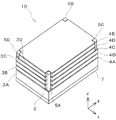
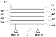
- the speaker system 1 includes a piezoelectric drive unit 10 having piezoelectric layers 3A, 3B, 3C, 3D made of, for example, lead zirconate titanate (PZT) and the like, and 4 bits.
- the digital signal IS is converted into four voltage signals (bit string data signal BS), and the voltage signal applied to each of the piezoelectric layers 3A to 3D is output according to the signal converted by the signal converter 11. And an output unit 12.
- the piezoelectric layers 3A to 3D are stacked on the substrate 2 in this order using the semiconductor manufacturing technique with the electrode layers 4B, 4C, and 4D interposed therebetween.
- An electrode layer 4A is formed below the lowermost piezoelectric layer 3A, and an electrode layer 4E is formed above the uppermost piezoelectric layer 3D.
- the piezoelectric layer 3A is driven by a voltage between the electrode layers 4A and 4B, the piezoelectric layer 3B is driven by a voltage between the electrode layers 4B and 4C, and the piezoelectric layer 3C is driven by a voltage between the electrode layers 4C and 4D.
- the piezoelectric layer 3D is driven by a voltage between the electrode layers 4D and 4E.
- the piezoelectric layers 3A, 3B, 3C, 3D expand and contract by driving the voltages applied to the electrode layers 4A, 4B, 4C, 4D, 4E.
- substrate 2 is formed with the raw material (for example, silicon) which does not expand-contract even if a voltage is applied.
- the polarities of the piezoelectric layers 3A to 3D are indicated by arrows. As indicated by these arrows, the piezoelectric layers 3A and 3C have an upward polarity, while the piezoelectric layers 3B and 3D have a downward polarity. Since the piezoelectric layers 3A to 3D are laminated in such a direction, if a voltage is applied so that the electrode layers 4B and 4D have a high potential and the electrode layers 4A, 4C and 4E have a low potential, the piezoelectric layers 3A to 3D are piezoelectric. The layers 3A to 3D are expanded, and the piezoelectric layers 3A to 3D are contracted when a reverse voltage is applied.
- each of the piezoelectric layers 3A to 3D has a rectangular flat plate shape with the same area, a uniform thickness, and the same thickness. Therefore, if the same voltage is applied to each of the piezoelectric layers 3A to 3D, the amount of expansion / contraction becomes the same.
- a voltage of 0 or a constant value (drive voltage) other than 0 is applied to each of the piezoelectric layers 3A to 3D.
- a state in which a non-zero drive voltage is applied to each of the piezoelectric layers 3A to 3D is referred to as an on state
- a state in which the drive voltage applied to each of the piezoelectric layers 3A to 3D is zero is referred to as an off state.
- the electrode layer 4A formed on the piezoelectric layer 3A is laminated with the substrate 2 that does not expand or contract even when a voltage is applied.
- the substrate 2 that does not expand or contract even when a voltage is applied.
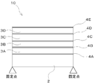
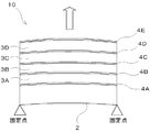
- each of the piezoelectric layers 3A to 3D is supported at two points at both ends (fixed at fixed points at both ends). Therefore, when the driving voltage applied to each of the piezoelectric layers 3A to 3D changes from off to on, the piezoelectric driving unit 10 is displaced from the state shown in FIG. 3A to the state shown in FIG. 3B. Specifically, the piezoelectric driving unit 10 is displaced in a bow shape in a direction indicated by an arrow in FIG. 3B.
- the piezoelectric driving unit 10 when the driving voltage is turned on, the piezoelectric driving unit 10 is bent and displaced (bending displacement) in the direction of the arrow, that is, in the direction in which the piezoelectric layers 3A to 3D are stacked. Due to this bending displacement, the piezoelectric drive unit 10 generates sound.
- the displacement amount of each of the piezoelectric layers 3A to 3D when the drive voltage is changed from OFF to ON is defined as a.
- the total displacement of the piezoelectric layers 3A to 3D is any one of a, 2a, 3a, and 4a in the positive direction (for example, the arrow direction shown in FIG. 3B) depending on the number of piezoelectric layers for which the drive voltage is turned on.
- any one of ⁇ a, ⁇ 2a, ⁇ 3a, and ⁇ 4a is set in the negative direction (for example, the direction opposite to the arrow direction shown in FIG. 3B). As shown in FIGS.
- the piezoelectric layers 3A to 3D are entirely changed by changing the displacement amount of each of the piezoelectric layers 3A to 3D by intermittently switching on and off the driving voltage for the piezoelectric layers 3A to 3D. It can vibrate and generate sound.
- the driving voltage of the piezoelectric layers 3A to 3D may be switched on and off at the low frequency (with a long period).
- the driving voltages of the piezoelectric layers 3A to 3D may be switched on and off at a high sound frequency (with a short period).
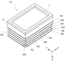
- cylindrical bumps 5A, 5B, 5C, and 5D are provided at the four corners of the piezoelectric drive unit 10.
- the bump 5A is electrically connected to the electrode layer 4A
- the bump 5B is electrically connected to the electrode layer 4B
- the bump 5C is electrically connected to the electrode layer 4C
- the bump 5D is electrically connected to the electrode layer 4D. Electrically connected.
- the voltage signal output from the output unit 12 is applied to the electrode layers 4A to 4E via wiring, lead wires (for example, bonding wires), bumps 5A to 5D, and the like.
- a voltage can be individually applied to the electrode layers 4A to 4E by the bumps 5A to 5D.
- rubber 7 is attached to the bottom surface of the substrate 2 in the piezoelectric driving unit 10.
- the rubber 7 is a frame-like body, and the piezoelectric drive unit 10 is attached to another member via the rubber 7. Thereby, the vibration component transmitted to the member from the piezoelectric drive part 10 can be reduced.
- the rubber 7 is not essential. Therefore, you may attach the piezoelectric drive part 10 which does not have the rubber
- the piezoelectric driving unit 10 not having the rubber 7 can be flip-chip mounted, for example, on the mounting surface of the wiring board using the bumps 5A to 5D.
- a wiring board is prepared in which an opening having a size that does not hinder the bending displacement of the piezoelectric drive unit 10 is formed on the mounting surface.
- the piezoelectric drive part 10 is mounted in the mounting surface of a wiring board in the state which the electrode layer 4E faced the opening.
- the bumps 5A to 5D of the piezoelectric drive unit 10 may be soldered to the electrodes provided on the mounting surface of the wiring board.
- the signal converter 11 inputs a 4-bit digital signal IS.
- the digital signal IS is a PCM (Pulse Code Modulation) signal output from, for example, an A / D converter.
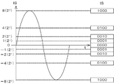
- a 4-bit digital signal IS takes values from ⁇ 8 ( ⁇ 2 3 ) to +8 (+2 3 ) in decimal numbers.
- the absolute value of ⁇ 8 is expressed as a binary number (1000).
- the absolute value of ⁇ 4 is expressed as (0100) in binary
- the absolute value of ⁇ 2 is expressed as (0010) in binary
- the absolute value of ⁇ 1 is expressed in binary (0001 )
- And 0 is expressed as a binary number (0000). If the piezoelectric driving unit 10 is vibrated so as to follow the signal waveform of FIG. 5, the piezoelectric driving unit 10 generates a sound based on the digital signal IS.
- the information indicating whether the digital signal IS is positive or negative is input to the signal converter 11 as another 1-bit signal.
- the signal converter 11 determines whether the digital signal IS is positive or negative based on the signal.
- the signal converter 11 converts the digital signal IS into a 4-bit bit string data signal BS indicating on / off of the drive voltage to each of the piezoelectric layers 3A to 3D.
- the bit string data signal BS is composed of bit string data indicating on / off of drive voltages applied to the piezoelectric layers 3A to 3D via the electrode layers 4A to 4E.
- the signal conversion unit 11 includes a calculation unit 20, a storage unit 21, an I / O unit 22, and an internal bus 23 as hardware.
- the arithmetic unit 20 is a processor that performs arithmetic processing for converting a 4-bit digital signal IS into a 4-bit bit string data signal BS.
- the storage unit 21 stores an arithmetic processing program executed by the arithmetic unit 20, and a digital signal IS and a bit string data signal BS to be operated.
- the arithmetic unit 20 performs the arithmetic processing by executing the arithmetic processing program stored in the storage unit 21.
- the I / O unit 22 receives the digital signal IS, stores it in the storage unit 21, and outputs the bit string data signal BS calculated by the calculation unit 20 and stored in the storage unit 21 to the output unit 12.
- the internal bus 23 connects the other components so that they can communicate with each other.
- the signal converter 11 performs conversion from the digital signal IS to the bit string data signal BS.
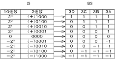
- this conversion for example, as shown in FIG. 7, when the digital signal IS is +8 (2 3 ) in decimal, the bit string data signal BS becomes (1111) in binary. This value indicates that all the drive voltages of the piezoelectric layers 3A to 3D are turned on.
- the bit string data signal BS is (0111) in binary number. This value indicates that all the drive voltages of the piezoelectric layers 3A to 3C are turned on.
- the bit string data signal BS is (0011) in binary number. This value indicates that all the drive voltages of the piezoelectric layers 3A and 3B are turned on.
- the bit string data signal BS is a binary number (0001). This value indicates that the drive voltage of the piezoelectric layer 3A is turned on.
- the bit string data signal BS is binary (0000). This value indicates that all the drive voltages of the piezoelectric layers 3A to 3D are turned off.
- the drive voltage applied to the piezoelectric layers 3A to 3D has a reverse polarity, and is represented as -1 in FIG.
- the signal conversion unit 11 has a digital signal IS whose absolute value in decimal number is 2 k ⁇ 1 (k is an integer of 1 ⁇ k ⁇ n) (in the present embodiment, 2 0 , 2 1 and 2 2 ), a signal composed of n-bit data obtained by combining k-bit data indicating driving voltage on and nk-bit data indicating driving voltage off is bit string data. Generated as signal BS.
- the signal conversion unit 11 detects a bit digit having a value of 1 in the digital signal IS as shown in FIG. Further, the signal conversion unit 11 sets a value of a bit lower than the detected bit digit as a value indicating ON of the driving voltage, and sets a value of a bit higher than the detected bit digit as a value indicating OFF of the driving voltage. Is generated as the bit string data signal BS.
- the output unit 12 outputs a drive voltage applied to each of the piezoelectric layers 3A to 3D in the piezoelectric drive unit 10 according to the value of each bit of the bit string data signal BS converted by the signal conversion unit 11. Specifically, the output unit 12 applies a driving voltage to each of the piezoelectric layers 3A to 3D by individually outputting voltage signals to the electrode layers 4A to 4E. By applying the driving voltage, the piezoelectric layers 3A to 3D vibrate, and the piezoelectric driving unit 10 generates sound according to the digital signal IS.
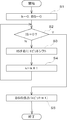
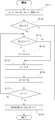
- the arithmetic unit 20 sets the variable k to 0 and sets the bit string data signal BS to 0 (step S1).
- the arithmetic unit 20 determines whether or not the digital signal IS is 0 (step S2). If the digital signal is 0 (step S2; Yes), the arithmetic unit 20 outputs the bit string data signal BS at that time to the output unit 12 (step S5). Here, “0000” is output as the bit string data signal BS.
- step S2 when the digital signal IS is not 0 (step S2; No), the arithmetic unit 20 shifts the digital signal IS by 1 bit to the right (step S3) and increments the counter value k by 1 (step S4). .
- step S5 the process ends.
- the signal conversion unit 11 performs the above-described conversion process every time the digital signal IS is input, and outputs the bit string data signal BS to the output unit 12.
- the output unit 12 outputs a voltage signal to each of the electrode layers 4A to 4E in accordance with the input bit string data signal BS.
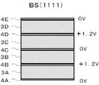
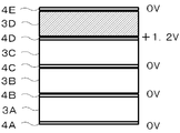
- the output unit 12 sets the voltage at which the electrode layer 4A is 0V and the electrode layers 4B to 4E are + 1.2V.
- a signal is output to the electrode layers 4A to 4E.
- a voltage signal in which the electrode layer 4A is set to 0V and the electrode layers 4B to 4E are set to -1.2V may be output to the electrode layers 4A to 4E.
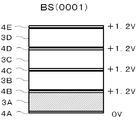
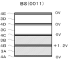
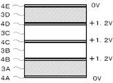
- the output unit 12 sets the electrode layer 4B to + 1.2V and sets the electrode layers 4A, 4C, and 4E to 0V. Voltage signals to be output to the electrode layers 4A to 4E.
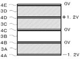
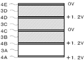
- the output unit 12 sets the electrode layers 4A and 4C to 0 V, and sets the electrode layers 4B, 4D, and 4E to +1. A voltage signal of 2V is output to the electrode layers 4A to 4E. As shown in FIG. 9B, when the bit string data signal BS is binary (0011), the output unit 12 sets the electrode layers 4A and 4C to 0 V, and sets the electrode layers 4B, 4D, and 4E to +1. A voltage signal of 2V is output to the electrode layers 4A to 4E. As shown in FIG.
- the output unit 12 sets the electrode layers 4A, 4C, and 4E to 0V, and sets the electrode layers 4B and 4D to +1.
- a voltage signal of 2V is output to the electrode layers 4A to 4E.
- + 1.2V may be set to -1.2V.
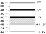
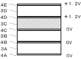
- voltage signals as shown in FIGS. 10A to 10C may be applied to the electrode layers 4A to 4E.
- how to apply voltage signals to the piezoelectric layers 3A to 3D when the bit string data signal BS is binary (0011) is not limited to that shown in FIG. 9B.
- voltage signals as shown in FIGS. 11A to 11C may be applied to the electrode layers 4A to 4E.
- the way of applying voltage signals to the piezoelectric layers 3A to 3D when the bit string data signal BS is binary (0111) is not limited to that shown in FIG. 9C.
- voltage signals as shown in FIGS. 12A to 12C may be applied to the electrode layers 4A to 4E.
- the output unit 12 includes a switching circuit 12A and a setting unit 12B.
- the switching circuit 12A receives the bit string data signal BS and outputs output signals to the electrode layers 4A to 4E.
- the setting unit 12B sets the pattern in which the voltage signal is supplied to the electrode layers 4A to 4E among the voltage patterns as shown in FIGS. 9A to 12C.
- the setting unit 12B Prior to the input of the digital signal IS, sets the bit position of the data indicating the drive voltage on and the bit position of the data indicating the drive voltage off in the switching circuit 12A of the output unit 12 in advance. Can do. By making it possible to change the bit position in advance, it is possible to finely adjust the sound generated by the piezoelectric drive unit 10.
- n-bit stacked piezoelectric layers 3A to 3D are bent and displaced in the direction in which the piezoelectric layers 3A to 3D are stacked, so that n-bit A bending displacement corresponding to the weight obtained by converting the digital signal IS into a decimal number can be obtained, and a desired sound pressure can be generated. Therefore, in order to generate sound corresponding to an n-bit digital signal, it is not necessary to arrange and stack the piezoelectric laminated structures laminated according to the bit digits in parallel. Thereby, further miniaturization, weight reduction, and low power consumption of the speaker can be realized.
- the number of stacked piezoelectric layers 3A to 3D can be reduced, so that the manufacturing cost of the speaker system 1 can be reduced.
- Embodiment 2 FIG. Next, a second embodiment of the present invention will be described.
- the digital signal IS is not limited to that according to the first embodiment. For example, some have a bit pattern as shown in FIG.
- the 4-bit digital signal IS takes a value from ⁇ 4 ( ⁇ 2 2 ) to +4 (+2 2 ). As shown in FIG. 13, in the digital signal IS, +4 is expressed as (0100) in binary. Similarly, in the digital signal IS, +3 is expressed as a binary number (0011), +2 is expressed as a binary number (0010), +1 is expressed as a binary number (0001), and 0 is expressed as a binary number (0000). ). Further, a negative number in the digital signal IS is a two's complement of a positive number, and the most significant bit indicates positive or negative. In this embodiment, a case where a digital signal IS having the bit pattern shown in FIG. 13 is input will be described.
- the hardware of the signal conversion unit 11 is the same as that shown in FIG.
- the signal converter 11 converts a digital signal IS having a bit pattern as shown in FIG. 13 into a bit string data signal BS shown in FIG.
- the computing unit 20 converts +4, +3, +2, +1, and 0 into (1111), (0111), (0011), (0001), and (0000) in binary numbers according to the table shown in FIG.
- the arithmetic unit 20 converts the other negative values into bit string data that is the corresponding two's complement of the positive number.
- a signal composed of bit data is generated as a bit string data signal BS.
- the signal conversion unit 11 obtains a number m (m is an integer of 0 ⁇ m ⁇ n) corresponding to the weight of the bit digit having a value of 1 in the absolute value in the binary number of the digital signal IS, and calculates m bits.
- a signal having a value indicating ON of the drive voltage and a value indicating nm bits indicating OFF of the drive voltage is generated as the bit string data signal BS.
- the bit digit weight is defined as follows.
- the weight of the third digit and the fourth digit is 2 2. 2 and 3 . That is, the weight of the n-th bit is 2 n .
- the arithmetic unit 20 sets the counter value j to 1, sets the variable m to 0, sets the variable a to 1, and sets the bit string data signal BS to 0 (step S11). .
- the arithmetic unit 20 determines whether or not the digital signal IS is 0 (step S12).
- the arithmetic unit 20 outputs a bit string data signal BS in which m bits are 1 and n ⁇ m bits are 0 among n bits (step S18). . That is, the bit string data signal BS (0000) corresponding to the digital signal IS (0000) is output.
- the arithmetic unit 20 determines whether or not the digital signal IS [j] is 1 (step S13).
- the digital signal IS [j] is the j-th digit of the digital signal IS (j is an integer of 1 ⁇ j ⁇ n). Only when the digital signal IS [j] is 1 (step S13; Yes), the arithmetic unit 20 substitutes a value for adding the variable a to the variable m into the variable m (step S14).
- step S15 increments the counter value j by 1 (step S15), and substitutes a value obtained by multiplying the variable a by 2 for the variable a (step S16).
- step S16 substitutes a value obtained by multiplying the variable a by 2 for the variable a (step S16).
- step S17 determines whether or not the counter value j is n (step S17). Thereafter, unless the counter value j becomes n in step S17 (step S17; No), step S13 ⁇ S15 ⁇ S16 ⁇ S17 or step S13 ⁇ S14 ⁇ S15 ⁇ S16 ⁇ S17 is repeated.
- the arithmetic unit 20 When the counter value j is n (step S17; Yes), the arithmetic unit 20 outputs a bit string data signal BS in which m bits are 1 among n bits, that is, all bits up to the m-th bit are 1. (Step S18).
- the signal conversion unit 11 performs the above-described conversion process every time the digital signal IS is input, and outputs the bit string data signal BS to the output unit 12.
- the output unit 12 outputs a voltage signal to each of the electrode layers 4A to 4E in accordance with the input bit string data signal BS.
- Embodiment 3 FIG. Next, a third embodiment of the present invention will be described.
- the 4-bit digital signal IS takes a value from ⁇ 4 ( ⁇ 2 2 ) to +4 (+2 2 ).
- +4 is expressed as (0100) in binary.
- +2 is expressed as a binary number (0010)
- +1 is expressed as a binary number (0001)
- 0 is expressed as a binary number (0000).
- a negative number in the digital signal IS is a two's complement of a positive number, and the most significant bit indicates positive or negative.
- the hardware of the signal conversion unit 11 is the same as that shown in FIG.
- the signal converter 11 converts a digital signal IS having a bit pattern as shown in FIG. 16 into a bit string data signal BS shown in FIG.
- the arithmetic unit 20 converts +4, +2, +1, and 0 into binary numbers (1111), (0011), (0001), and (0000), respectively.
- the other negative values are converted into bit string data that is the two's complement of the corresponding positive number.
- the signal converter 11 When the absolute value in decimal number of the digital signal IS is 0, the signal converter 11 generates a signal composed of n-bit data indicating that the drive voltage is turned off as the bit string data signal BS. Further, when the absolute value in decimal of the digital signal IS is 2 n ⁇ 2 , the signal conversion unit 11 generates a signal composed of n-bit data indicating that the drive voltage is on as the bit string data signal BS.
- the signal conversion unit 11 uses the absolute value in the binary number of the digital signal IS.
- a number m corresponding to the weight of a bit digit having a value of 1 is obtained, and a signal having an m-bit value as a value indicating that the drive voltage is on and an nm bit value as a value indicating that the drive voltage is off, It is generated as a bit string data signal BS.
- the arithmetic unit 20 sets a variable m to 0 and sets a bit string data signal BS to 0 (step S21).
- the arithmetic unit 20 determines whether or not the digital signal IS is 0 (step S22). If the digital signal is 0 (step S22; Yes), the calculation unit 20 outputs the bit string data signal BS (0000) at that time to the output unit 12 (step S27).
- step S22 When the digital signal IS is not 0 (step S22; No), the arithmetic unit 20 shifts the digital signal IS to the right by 1 bit (step S23). Further, the computing unit 20 adds 1 to the variable m and substitutes it into the variable m (step S24), and determines whether or not the variable m is equal to n ⁇ 1 (step S25).
- step S25 Yes
- the computing unit 20 1 is added to m and assigned to variable m (step S26).
- step S26 On the other hand, when the variable m is not the same as n ⁇ 1 (step S25; No), step S26 is skipped.
- step S22 Thereafter, while the digital signal IS bit-shifted to the right does not become 0 (step S22; No), steps S22 ⁇ S23 ⁇ S24 ⁇ S25 ⁇ S26 are repeated.
- step S22 the arithmetic unit 20 outputs a bit string data signal BS in which m bits at that time are 1 and nm bits are 0. (Step S27), the process ends.
- the signal conversion unit 11 performs the above-described conversion process every time the digital signal IS is input, and outputs the bit string data signal BS to the output unit 12.
- the output unit 12 outputs a voltage signal to each of the electrode layers 4A to 4E in accordance with the input bit string data signal BS.
- the binary bit operation is used to convert the digital signal IS into the bit string data signal BS.
- Conversion tables as shown in FIG. 7, FIG. 14 and FIG. 17 are held in the signal conversion unit 11, and signal conversion is performed by referring to the conversion table (bit string data signal BS corresponding to the input digital signal IS). May be performed. In this way, it is not necessary to perform bit operation, so that the time required for conversion can be further shortened.
- the signal conversion unit 11 performs the above-described conversion process every time the digital signal IS is input, and outputs the bit string data signal BS to the output unit 12.
- the output unit 12 outputs voltage signals to the electrode layers 4A to 4E in the patterns shown in FIGS. 9A to 12C according to the input bit string data signal BS.
- the digital signal is a 4-bit digital signal and the number of stacked piezoelectric layers is 4.
- the present invention is not limited to this.
- it can be 8 bits, 16 bits, or the like.
- the number of bits of the digital signal and the number of stacked piezoelectric layers can be n (n is a natural number of 2 or more).
- the above-described arithmetic processing in the signal converting unit 11 converts the digital signal IS into the bit string data signal BS without converting the digital signal IS into a decimal number, and the arithmetic time can be shortened.
- the calculation processing of the signal conversion unit 11 is not limited to that according to the above embodiment.
- the bit string data signal BS may be obtained by setting the initial value of each bit of the bit string data signal BS to 1 and shifting 0 to the right according to the value of the digital signal IS.
- the arithmetic processing of the signal conversion unit 11 is not software, for example, a special purpose logic device (for example, ASIC (Application Specific Integrated Circuit)) and a configurable logic device (for example, SPLD (Simple Programmable Logic Device), CPLD). (Complex Programmable Logic Device)), FPGA (Field Programmable Gate Array), or the like may be used.
- a special purpose logic device for example, ASIC (Application Specific Integrated Circuit)
- SPLD Simple Programmable Logic Device
- CPLD Complex Programmable Logic Device
- FPGA Field Programmable Gate Array
- the substrate 2 is laminated on the entire surface of the electrode layer 4E formed on the piezoelectric layer 3A, so that each of the piezoelectric layers 3A to 3D is supported at two points at both ends (both ends).
- a support method widely applied to general names “unimorph actuator” and “bimorph actuator”, that is, two regions as shown in FIG. Support or one-point support as shown in FIG. 19C may be realized by the piezoelectric drive unit 10.
- the two-point support is a method of supporting the piezoelectric layers 3A to 3D at both ends of the substrate 2 that is laminated with offset, and the one-point support is a method in which the piezoelectric layers 3A to 3D are supported at the central portion of the substrate 2. It is a method to support.
- FIG. 19A when each of the piezoelectric layers 3A to 3D is supported at two points offset inward from the end of the piezoelectric drive unit 10, as shown in FIG. 19B, from the end of the electrode layer 4E. What is necessary is just to laminate
- FIG. 19C when each of the piezoelectric layers 3A to 3D is supported at one point, the substrate 2 may be laminated at, for example, the central portion of the electrode layer 4E as shown in FIG. 19D.
- the piezoelectric layers 3A to 3D are arranged so that the polarities of the adjacent piezoelectric layers are reversed.
- the piezoelectric layers 3A to 3D have the same polarity, and the electrode layers 4A, 4B, 4C, 4D, and 4E are applied stepwise such as 0V, + 1.2V1, + 2.4V, + 3.6V, and + 4.8V, respectively.
- the piezoelectric layers 3A to 3D may be driven by applying a driving voltage that increases or decreases at regular intervals.
- the present invention can be applied to an earphone that needs to be miniaturized, a small speaker mounted on a vehicle, and the like.
- 1 speaker system 2 substrates, 3A, 3B, 3C, 3D piezoelectric layer, 4A, 4B, 4C, 4D, 4E electrode layer, 5A, 5B, 5C, 5D bump, 7 rubber, 10 piezoelectric drive unit, 11 signal conversion unit , 12 output unit, 12A switching circuit, 12B setting unit, 20 operation unit, 21 storage unit, 22 I / O unit, 23 internal bus, BS bit string data signal, IS digital signal
Landscapes
- Physics & Mathematics (AREA)
- Engineering & Computer Science (AREA)
- Acoustics & Sound (AREA)
- Signal Processing (AREA)
- Health & Medical Sciences (AREA)
- Otolaryngology (AREA)
- Circuit For Audible Band Transducer (AREA)
- Piezo-Electric Transducers For Audible Bands (AREA)
Abstract
Une unité d'entraînement piézoélectrique (10) a n (n est un entier de 2 ou plus) couches piézoélectriques (3A à 3D) empilées à l'aide de couches d'électrodes (4B à 4D) interposées entre ces dernières, des couches d'électrodes (4A, 4E) étant en outre formées sur le fond de la couche piézoélectrique (3A) de la couche inférieure et sur le dessus de la couche piézoélectrique (3D) de la couche supérieure, l'unité d'entraînement piézoélectrique (10) se pliant et étant déplacée dans la direction dans laquelle les couches piézoélectriques sont empilées. Une unité de conversion de signal (11) convertit un signal numérique de n bits (IS) en n bits d'un signal de données de chaîne de bits (BS) comprenant des données de bit indiquant l'état de marche et d'arrêt d'une tension de commande qui est appliquée à chacune des couches piézoélectriques (3A à 3D) par l'intermédiaire des couches d'électrodes (4A à 4B). Une unité de sortie (12) délivre, en fonction de la valeur de chaque bit du signal de données de chaîne de bits (BS) obtenue par la conversion effectuée par l'unité de conversion de signal (11), la tension d'attaque appliquée à chacune des couches piézoélectriques (3A à 3D).
Priority Applications (2)
| Application Number | Priority Date | Filing Date | Title |
|---|---|---|---|
| US16/090,801 US10638234B2 (en) | 2016-04-15 | 2017-04-12 | Speaker system |
| JP2018512046A JP6648821B2 (ja) | 2016-04-15 | 2017-04-12 | スピーカシステム |
Applications Claiming Priority (2)
| Application Number | Priority Date | Filing Date | Title |
|---|---|---|---|
| JP2016-082490 | 2016-04-15 | ||
| JP2016082490 | 2016-04-15 |
Publications (1)
| Publication Number | Publication Date |
|---|---|
| WO2017179616A1 true WO2017179616A1 (fr) | 2017-10-19 |
Family
ID=60042196
Family Applications (1)
| Application Number | Title | Priority Date | Filing Date |
|---|---|---|---|
| PCT/JP2017/014968 Ceased WO2017179616A1 (fr) | 2016-04-15 | 2017-04-12 | Système de haut-parleur |
Country Status (3)
| Country | Link |
|---|---|
| US (1) | US10638234B2 (fr) |
| JP (1) | JP6648821B2 (fr) |
| WO (1) | WO2017179616A1 (fr) |
Families Citing this family (2)
| Publication number | Priority date | Publication date | Assignee | Title |
|---|---|---|---|---|
| WO2017179616A1 (fr) * | 2016-04-15 | 2017-10-19 | 第一精工株式会社 | Système de haut-parleur |
| CN119233168A (zh) * | 2024-09-12 | 2024-12-31 | 地球山(苏州)微电子科技有限公司 | 数字发声方法及数字发声装置 |
Citations (3)
| Publication number | Priority date | Publication date | Assignee | Title |
|---|---|---|---|---|
| JPS58202697A (ja) * | 1982-05-21 | 1983-11-25 | Hitachi Ltd | 発音装置 |
| JP2011211725A (ja) * | 2006-05-21 | 2011-10-20 | Trigence Semiconductor Inc | デジタルアナログ変換装置 |
| JP2015029313A (ja) * | 2009-12-16 | 2015-02-12 | 株式会社 Trigence Semiconductor | スピーカーボックス |
Family Cites Families (27)
| Publication number | Priority date | Publication date | Assignee | Title |
|---|---|---|---|---|
| US3947708A (en) * | 1974-11-27 | 1976-03-30 | Gte Laboratories Incorporated | Apparatus for and method of converting from a digital signal to an acoustic wave using a piezoelectric beam |
| JPS58104598A (ja) | 1981-11-17 | 1983-06-22 | Hitachi Ltd | 発音装置 |
| JPH02141096A (ja) | 1988-11-21 | 1990-05-30 | Murata Mfg Co Ltd | 圧電スピーカ |
| US5159226A (en) * | 1990-07-16 | 1992-10-27 | Atlantic Richfield Company | Torsional force transducer and method of operation |
| WO1992001955A1 (fr) * | 1990-07-16 | 1992-02-06 | Atlantic Richfield Company | Transducteur de force de torsion et procede de fonctionnement |
| JPH0815101B2 (ja) | 1991-07-04 | 1996-02-14 | 日立電線株式会社 | ケーブル端末接続部 |
| US5157730A (en) * | 1991-10-15 | 1992-10-20 | Hualon Microelectrics Corporation | Pulse rate modulation type piezoelectric crystal driver device |
| US5347587A (en) * | 1991-11-20 | 1994-09-13 | Sharp Kabushiki Kaisha | Speaker driving device |
| US6492761B1 (en) * | 1998-01-20 | 2002-12-10 | Ericsson Inc. | Digital piezoelectric transducers and methods |
| DE602004024104D1 (de) * | 2003-09-25 | 2009-12-24 | Kyocera Corp | Mehrschichtiges piezoelektrisches bauelement |
| JP4284391B2 (ja) | 2004-04-16 | 2009-06-24 | ソニー株式会社 | 圧電バイモルフ素子の支持構造 |
| JP5396588B2 (ja) * | 2008-06-16 | 2014-01-22 | 株式会社 Trigence Semiconductor | デジタルスピーカー駆動装置,デジタルスピーカー装置,アクチュエータ,平面ディスプレイ装置及び携帯電子機器 |
| DE102010009453A1 (de) * | 2010-02-26 | 2011-09-01 | Fraunhofer-Gesellschaft zur Förderung der angewandten Forschung e.V. | Schallwandler zum Einsetzen in ein Ohr |
| JP2012191834A (ja) * | 2011-02-23 | 2012-10-04 | Oki Data Corp | 高圧電源装置および画像形成装置 |
| WO2012117831A1 (fr) * | 2011-03-01 | 2012-09-07 | 株式会社村田製作所 | Élément piézoélectrique et dispositif piézoélectrique l'utilisant |
| JP5708167B2 (ja) * | 2011-04-06 | 2015-04-30 | コニカミノルタ株式会社 | 超音波探触子及び超音波診断装置 |
| US9571926B2 (en) * | 2011-04-08 | 2017-02-14 | Christopher Technology (Shanghai) Limited | High-efficiency low-voltage-power-supply high-power-output audio driver architecture |
| JP5769542B2 (ja) * | 2011-08-18 | 2015-08-26 | 株式会社沖データ | 高圧電源装置及び画像形成装置 |
| US9762150B2 (en) * | 2011-09-13 | 2017-09-12 | Mide Technology Corporation | Self-powered sensor system |
| IN2014DN03351A (fr) * | 2011-10-25 | 2015-06-26 | Trigence Semiconductor Inc | |
| US20130342078A1 (en) * | 2012-10-03 | 2013-12-26 | U.S. Army Research Laboratory Attn: Rdrl-Loc-I | Apparatus and method of making a multi-layered piezoelectric actuator |
| CN104823459B (zh) * | 2012-11-28 | 2018-04-17 | 歌乐株式会社 | 数字扬声器系统以及数字扬声器系统的接线方法 |
| US9641937B2 (en) * | 2013-02-28 | 2017-05-02 | Clarion Co., Ltd. | Digital amplifier, three-value signal output method and speaker |
| JP2014240789A (ja) * | 2013-06-12 | 2014-12-25 | ソニー株式会社 | 圧電デバイス及び電子機器 |
| CN103701465B (zh) * | 2013-12-02 | 2016-09-21 | 苏州上声电子有限公司 | 一种基于多比特△—σ调制的数字扬声器系统实现方法和装置 |
| US10433067B2 (en) * | 2015-07-22 | 2019-10-01 | Audio Pixels Ltd. | DSR speaker elements and methods of manufacturing thereof |
| WO2017179616A1 (fr) * | 2016-04-15 | 2017-10-19 | 第一精工株式会社 | Système de haut-parleur |
-
2017
- 2017-04-12 WO PCT/JP2017/014968 patent/WO2017179616A1/fr not_active Ceased
- 2017-04-12 JP JP2018512046A patent/JP6648821B2/ja active Active
- 2017-04-12 US US16/090,801 patent/US10638234B2/en active Active
Patent Citations (3)
| Publication number | Priority date | Publication date | Assignee | Title |
|---|---|---|---|---|
| JPS58202697A (ja) * | 1982-05-21 | 1983-11-25 | Hitachi Ltd | 発音装置 |
| JP2011211725A (ja) * | 2006-05-21 | 2011-10-20 | Trigence Semiconductor Inc | デジタルアナログ変換装置 |
| JP2015029313A (ja) * | 2009-12-16 | 2015-02-12 | 株式会社 Trigence Semiconductor | スピーカーボックス |
Also Published As
| Publication number | Publication date |
|---|---|
| JP6648821B2 (ja) | 2020-02-14 |
| JPWO2017179616A1 (ja) | 2019-02-21 |
| US10638234B2 (en) | 2020-04-28 |
| US20190124451A1 (en) | 2019-04-25 |
Similar Documents
| Publication | Publication Date | Title |
|---|---|---|
| US10484784B1 (en) | Sound producing apparatus | |
| US20170033274A1 (en) | Microelectromechanical apparatus for generating a physical effect | |
| US5856956A (en) | Piezoelectric acoustic transducer | |
| CN102972046B (zh) | 振荡装置和电子设备 | |
| CN111755592A (zh) | 柔性振动模块和包括该柔性振动模块的显示设备 | |
| CN113015071B (zh) | 扬声器和包括该扬声器的显示设备 | |
| CN110071658B (zh) | 压电式换能器 | |
| JP6648821B2 (ja) | スピーカシステム | |
| CN110957415A (zh) | 复合压电致动器 | |
| JP2023105776A (ja) | 圧電スピーカ | |
| CN102544350B (zh) | 压电致动器 | |
| EP2856769B1 (fr) | Système, procédé et produit-programme informatique pour contrôler un groupe de réseaux d'actionneurs en vue de produire un effet physique | |
| US9680084B2 (en) | Piezoelectric element driving apparatus and method, and piezoelectric system using the same | |
| JP5134431B2 (ja) | 発音体 | |
| WO2019059101A1 (fr) | Unité de vibration | |
| JP2013039016A (ja) | エネルギー転換モジュール | |
| US12219335B2 (en) | Apparatus for outputting a sound | |
| US10582304B2 (en) | Diaphragm element arrangement and related method | |
| US20130039516A1 (en) | Sound Production Component | |
| JPH06275884A (ja) | 圧電素子 | |
| US20150349235A1 (en) | Waveform generating apparatus, signal generating circuit, piezoelectric driving apparatus and method, and electronic device using the same | |
| KR20150134627A (ko) | 피에조 액추에이터 구동 장치 및 그 구동 방법 | |
| KR20190127126A (ko) | 압전 소자, 이 소자를 포함하는 압전 액츄에이터, 및 이 액츄에이터를 포함하는 압전 모듈 | |
| JP2017131052A (ja) | 圧電素子駆動装置 | |
| JP2000070851A (ja) | 容量性負荷の駆動装置 |
Legal Events
| Date | Code | Title | Description |
|---|---|---|---|
| ENP | Entry into the national phase |
Ref document number: 2018512046 Country of ref document: JP Kind code of ref document: A |
|
| NENP | Non-entry into the national phase |
Ref country code: DE |
|
| 121 | Ep: the epo has been informed by wipo that ep was designated in this application |
Ref document number: 17782429 Country of ref document: EP Kind code of ref document: A1 |
|
| 122 | Ep: pct application non-entry in european phase |
Ref document number: 17782429 Country of ref document: EP Kind code of ref document: A1 |