WO2017179676A1 - Antenne - Google Patents
Antenne Download PDFInfo
- Publication number
- WO2017179676A1 WO2017179676A1 PCT/JP2017/015201 JP2017015201W WO2017179676A1 WO 2017179676 A1 WO2017179676 A1 WO 2017179676A1 JP 2017015201 W JP2017015201 W JP 2017015201W WO 2017179676 A1 WO2017179676 A1 WO 2017179676A1
- Authority
- WO
- WIPO (PCT)
- Prior art keywords
- conductor
- gap
- resonator
- antenna
- tip portion
- Prior art date
- Legal status (The legal status is an assumption and is not a legal conclusion. Google has not performed a legal analysis and makes no representation as to the accuracy of the status listed.)
- Ceased
Links
Images








Classifications
-
- H—ELECTRICITY
- H01—ELECTRIC ELEMENTS
- H01Q—ANTENNAS, i.e. RADIO AERIALS
- H01Q9/00—Electrically-short antennas having dimensions not more than twice the operating wavelength and consisting of conductive active radiating elements
- H01Q9/04—Resonant antennas
- H01Q9/0485—Dielectric resonator antennas
-
- H—ELECTRICITY
- H01—ELECTRIC ELEMENTS
- H01Q—ANTENNAS, i.e. RADIO AERIALS
- H01Q9/00—Electrically-short antennas having dimensions not more than twice the operating wavelength and consisting of conductive active radiating elements
- H01Q9/04—Resonant antennas
- H01Q9/30—Resonant antennas with feed to end of elongated active element, e.g. unipole
-
- H—ELECTRICITY
- H01—ELECTRIC ELEMENTS
- H01Q—ANTENNAS, i.e. RADIO AERIALS
- H01Q1/00—Details of, or arrangements associated with, antennas
- H01Q1/12—Supports; Mounting means
- H01Q1/22—Supports; Mounting means by structural association with other equipment or articles
- H01Q1/24—Supports; Mounting means by structural association with other equipment or articles with receiving set
- H01Q1/241—Supports; Mounting means by structural association with other equipment or articles with receiving set used in mobile communications, e.g. GSM
- H01Q1/242—Supports; Mounting means by structural association with other equipment or articles with receiving set used in mobile communications, e.g. GSM specially adapted for hand-held use
- H01Q1/243—Supports; Mounting means by structural association with other equipment or articles with receiving set used in mobile communications, e.g. GSM specially adapted for hand-held use with built-in antennas
-
- H—ELECTRICITY
- H01—ELECTRIC ELEMENTS
- H01Q—ANTENNAS, i.e. RADIO AERIALS
- H01Q1/00—Details of, or arrangements associated with, antennas
- H01Q1/36—Structural form of radiating elements, e.g. cone, spiral, umbrella; Particular materials used therewith
- H01Q1/38—Structural form of radiating elements, e.g. cone, spiral, umbrella; Particular materials used therewith formed by a conductive layer on an insulating support
-
- H—ELECTRICITY
- H01—ELECTRIC ELEMENTS
- H01Q—ANTENNAS, i.e. RADIO AERIALS
- H01Q1/00—Details of, or arrangements associated with, antennas
- H01Q1/48—Earthing means; Earth screens; Counterpoises
-
- H—ELECTRICITY
- H01—ELECTRIC ELEMENTS
- H01Q—ANTENNAS, i.e. RADIO AERIALS
- H01Q19/00—Combinations of primary active antenna elements and units with secondary devices, e.g. with quasi-optical devices, for giving the antenna a desired directional characteristic
- H01Q19/22—Combinations of primary active antenna elements and units with secondary devices, e.g. with quasi-optical devices, for giving the antenna a desired directional characteristic using a secondary device in the form of a single substantially straight conductive element
- H01Q19/26—Combinations of primary active antenna elements and units with secondary devices, e.g. with quasi-optical devices, for giving the antenna a desired directional characteristic using a secondary device in the form of a single substantially straight conductive element the primary active element being end-fed and elongated
-
- H—ELECTRICITY
- H01—ELECTRIC ELEMENTS
- H01Q—ANTENNAS, i.e. RADIO AERIALS
- H01Q7/00—Loop antennas with a substantially uniform current distribution around the loop and having a directional radiation pattern in a plane perpendicular to the plane of the loop
-
- H—ELECTRICITY
- H01—ELECTRIC ELEMENTS
- H01Q—ANTENNAS, i.e. RADIO AERIALS
- H01Q9/00—Electrically-short antennas having dimensions not more than twice the operating wavelength and consisting of conductive active radiating elements
- H01Q9/04—Resonant antennas
- H01Q9/0407—Substantially flat resonant element parallel to ground plane, e.g. patch antenna
- H01Q9/0414—Substantially flat resonant element parallel to ground plane, e.g. patch antenna in a stacked or folded configuration
Definitions
- the present invention relates to an antenna.
- the second resonator has the first conductor portion and the second conductor portion that is capacitively coupled to the first conductor portion via the gap
- the gap is narrowed.
- the capacity of the capacitive coupling portion sandwiching the gap increases, so that the antenna can be downsized.
- the radiation efficiency of the antenna may decrease.
- an object of one embodiment of the present invention is to provide an antenna that can achieve both reduction in size and improvement in radiation efficiency.
- a ground plane A first resonator connected to a feed point with respect to the ground plane; A second resonator that is fed in a non-contact manner by electromagnetic coupling by the first resonator;
- the second resonator includes a first conductor portion and a second conductor portion that is capacitively coupled to the first conductor portion via a gap.
- An antenna is provided in which the dielectric loss tangent of the base material portion on which the second resonator is formed is greater than 0 and less than or equal to 0.01.
- the dielectric loss tangent of the base material portion on which the second resonator is formed is greater than 0 and 0.01 or less, the radiation efficiency can be improved even if the gap is narrowed. . Therefore, both miniaturization of the antenna and improvement of the radiation efficiency can be achieved.
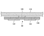
- FIG. 15 is a cross-sectional view schematically showing a peripheral portion of a radiating element in the antenna shown in FIG. 14. It is a top view which shows the part shown by FIG. 15 from the viewpoint from the conductor strip side with respect to a film. It is a figure which shows the antenna shown by FIG. 14 by planar view. It is a figure which shows the radiation element and conductor strip of the antenna shown by FIG. 17 by planar view. It is a figure which shows the electric power feeding element of the antenna shown by FIG. 17 by planar view. It is a figure which shows the dielectric constant and dielectric loss tangent of each material.
- FIG. 12 is a diagram illustrating an example of a result of calculation on a simulation of a relationship between a distance between a feeding element and a radiation element and radiation efficiency in the antenna configuration illustrated in FIGS.
- FIG. 1 is a perspective view showing an example of the configuration of a simulation model of the antenna 25 according to an embodiment.
- the antenna 25 is mounted on an electronic device.
- the electronic device performs wireless communication using the antenna 25.
- the electronic device on which the antenna 25 is mounted is, for example, a wireless communication module, a display device itself such as a stationary television or a personal computer, a device mounted on the display device, a mobile body itself, or a device mounted on the mobile body.
- a wireless communication module for example, a wireless communication module
- a display device itself such as a stationary television or a personal computer
- a device mounted on the display device a mobile body itself, or a device mounted on the mobile body.
- the mobile object include a portable terminal device, a vehicle such as an automobile, and a robot.
- Specific examples of the mobile terminal device include a mobile phone, a smartphone, a computer, a game machine, a television, a music and video player, and a wearable device.
- Specific examples of the wearable device include a wristwatch type, a pendant type, and a glasses type.
- the antenna 25 corresponds to, for example, a wireless communication standard such as Bluetooth (registered trademark) or a wireless LAN (Local Area Network) standard such as IEEE802.11ac.
- the antenna 25 is connected to the end 12 of the transmission line using the ground 14.
- transmission lines include microstrip lines, strip lines, coplanar waveguides with ground planes (coplanar waveguides having a ground plane disposed on the surface opposite to the conductor surface on which signal lines are formed), and coplanar strip lines. Etc.
- the antenna 25 includes a ground 14, a feeding element 21, and a radiating element 22.
- the ground 14 is an example of a ground plane.
- the ground outer edge 14 a is an example of a linear outer edge of the ground 14.
- the ground 14 is a ground pattern formed on the substrate 13 parallel to the XY plane, for example.
- the substrate 13 is a member whose main component is a dielectric.
- a specific example of the substrate 13 is an FR4 (Flame Retardant Type 4) substrate.
- the substrate 13 may be a flexible substrate having flexibility.
- the substrate 13 has a first substrate surface and a second substrate surface opposite to the first substrate surface.
- an electronic circuit is mounted on the first substrate surface, and a ground 14 is formed on the second substrate surface.
- the ground 14 may be formed on the surface of the first substrate or may be formed inside the substrate 13.
- the electronic circuit mounted on the substrate 13 is, for example, an integrated circuit including at least one of a reception function for receiving a signal via the antenna 25 and a transmission function for transmitting a signal via the antenna 25.
- the electronic circuit is realized by, for example, an IC chip.
- the feeding element 21 is an example of a first resonator connected to a feeding point with a ground plane as a reference.
- the feed element 21 is connected to the end 12 of the transmission line.
- the terminal end 12 is an example of a feeding point with the ground 14 as a ground reference.
- the power feeding element 21 may be disposed on the substrate 13 or may be disposed at a place other than the substrate 13.
- the power feeding element 21 is, for example, a conductor pattern formed on the first substrate surface of the substrate 13.
- the feeding element 21 extends in a direction away from the ground 14, and is connected to a feeding point (termination 12) with the ground 14 as a ground reference.
- the feeding element 21 is a linear conductor that can be fed to the radiating element 22 in a non-contact manner in a high frequency manner.
- a feeding element 21 formed in an L shape by a linear conductor extending in a direction perpendicular to the ground outer edge 14a and a linear conductor extending parallel to the ground outer edge 14a is shown. Illustrated.
- the power feeding element 21 extends from the end portion 21a with the terminal end 12 as a starting point, then bends at the bent portion 21c, and extends to the front end portion 21b.
- the tip portion 21b is an open end to which no other conductor is connected.
- the L-shaped feeding element 21 is illustrated in the drawing, the shape of the feeding element 21 may be other shapes such as a straight line shape, a meander shape, and a loop shape.
- the radiating element 22 is an example of a second resonator close to the first resonator.
- the radiating element 22 is disposed away from the power feeding element 21 and functions as a radiating conductor when the power feeding element 21 resonates.
- the radiating element 22 functions as a radiating conductor by being fed in a non-contact manner by electromagnetic coupling with the feeding element 21.
- Electromagnetic field coupling means non-contact coupling by electromagnetic waves.
- the radiating element 22 has a conductor portion extending along the ground outer edge 14a.
- conductor elements 41, 51, and 52 are shown as conductor portions.
- the conductor portion is located away from the ground outer edge 14a.
- the feeding element 21 and the radiating element 22 are arranged, for example, separated by a distance that allows electromagnetic coupling to each other.
- the radiating element 22 includes a power feeding unit that receives power from the power feeding element 21.
- a first conductor element 41 is shown as a power feeding unit.
- the radiating element 22 is fed in a non-contact manner by electromagnetic coupling through the feeding element 21 in the feeding section. By being fed in this way, the radiating element 22 functions as a radiating conductor of the antenna 25.
- the radiating element 22 is fed in a non-contact manner by electromagnetic coupling by the feeding element 21, so that a resonance current similar to that of the half-wavelength dipole antenna (a standing wave shape between one tip portion 23 and the other tip portion 24). Current distributed on the radiation element 22. That is, the radiating element 22 functions as a dipole antenna by being fed in a non-contact manner by electromagnetic coupling by the feeding element 21.
- the radiating element 22 includes a first conductor element 41, a second conductor element 51, and a third conductor element 52.
- the second conductor element 51 is an example of a first conductor portion.
- the third conductor element 52 is an example of a second conductor portion.
- the first conductor element 41 has one end connected to the second conductor element 51 and the other end connected to the third conductor element 52.
- the second conductor element 51 is folded and extended at the one end with respect to the first conductor element 41, and the third conductor element 52 is folded at the other end with respect to the first conductor element 41. Extend.
- the first tip portion 23 of the second conductor element 51 and the second tip portion 24 of the third conductor element 52 are separated from each other via a gap 60. That is, the shape of the radiating element 22 is an open loop that opens at the gap 60, and the radiating element 22 is an open loop resonant antenna having the gap 60.
- the first tip 23 of the second conductor element 51 is one tip of the radiating element 22, and the second tip 24 of the third conductor element 52 is the other tip of the radiating element 22. Part.
- the second conductor element 51 and the third conductor element 52 are capacitively coupled through the gap 60.
- the first tip portion 23 and the second tip portion 24 are capacitively coupled through the gap 60. That is, the radiating element 22 has a capacitive coupling portion in which the gap 60 is sandwiched between the first tip portion 23 and the second tip portion 24.
- the first tip portion 23 and the second tip portion 24 oppose each other in the longitudinal direction of the second conductor element 51 and the third conductor element 52.
- the gap 60 is formed between the first tip portion 23 and the second tip portion 24 in the longitudinal direction.
- the radiating element 22 is provided on the dielectric base 30.
- the base material part 30 is a board
- the shorter the gap length of the gap 60 the larger the capacitance of the capacitive coupling portion sandwiching the gap 60 between the second conductor element 51 and the third conductor element 52.
- the element 22 can be downsized.
- the antenna 25 can be downsized by reducing the size of the radiating element 22.
- the gap 60 is formed in a straight line, but may be formed in a comb-like interdigital structure.
- the radiation efficiency ⁇ represents the ratio of the radiated power to the power supplied to the antenna 25.
- the deterioration of the radiation efficiency ⁇ is caused by the dielectric loss tangent (tan ⁇ ) of the base material portion 30 on which the radiation element 22 is formed.
- the dielectric loss tangent (tan ⁇ ) of the base material portion 30 is set to be larger than 0 and 0.01 or less.
- the shortest distance between the feeding element 21 and the radiating element 22 is greater than 0 and 0.117 ⁇ ⁇ or less. Is preferable in terms of achieving both improvement of the efficiency and radiation efficiency ⁇ . More preferably, it is 0.07 ⁇ ⁇ or less, and further preferably 0.04 ⁇ ⁇ or less.
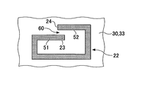
- FIG. 2 is a diagram showing an example of a surface arrangement configuration of the capacitive coupling portion in a plan view of the base material portion 30, and is shown from a viewpoint from the normal direction of the first surface 33 of the base material portion 30.
- the normal direction of the first surface 33 is a direction parallel to the Z axis (see FIG. 1).
- the radiating element 22 and the gap 60 are located on the first surface 33.
- the first tip portion 23 and the second tip portion 24 oppose each other in the element width direction of the second conductor element 51 and the third conductor element 52.
- the gap 60 is formed between the first tip portion 23 and the second tip portion 24 in the element width direction.
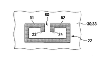
- FIG. 3 is a diagram showing another example of the surface arrangement configuration of the capacitive coupling portion in a plan view of the base material portion 30, and is shown from a viewpoint from the normal direction of the first surface 33 of the base material portion 30.
- the radiating element 22 and the gap 60 are located on the first surface 33.
- the first tip portion 23 and the second tip portion 24 oppose each other in the longitudinal direction of the second conductor element 51 and the third conductor element 52.
- the gap 60 is formed between the first tip portion 23 and the second tip portion 24 in the longitudinal direction.
- the first tip portion 23 bends at right angles to the longitudinal direction of the second conductor element 51, and the second tip portion 24 bends at right angles to the longitudinal direction of the third conductor element 52.
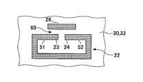
- FIG. 4 is a diagram showing another example of the surface arrangement configuration of the capacitive coupling portion in a plan view of the base material portion 30, and is shown from a viewpoint from the normal direction of the first surface 33 of the base material portion 30.
- the radiating element 22 and the gap 60 are located on the first surface 33.
- the antenna 25 includes a fourth conductor element 26 located on the first surface 33.
- the fourth conductor element 26 is an example of a third conductor portion.
- the fourth conductor element 26 is capacitively coupled to the second conductor element 51 and the third conductor element 52 via the gap 60.
- the first tip portion 23 and the second tip portion 24 face each other in the longitudinal direction of the second conductor element 51 and the third conductor element 52, and are capacitively coupled via the first gap 60. To do.
- the first gap 60 is formed between the first tip portion 23 and the second tip portion 24 in the longitudinal direction.
- the first tip portion 23 of the second conductor element 51 and one tip portion of the fourth conductor element 26 are opposed to each other in the element width direction of the second conductor element 51 and the fourth conductor element 26. , Capacitively coupled through the second gap 60.
- the second gap 60 is formed between the first tip portion 23 and the one tip portion in the element width direction.
- the second tip 24 of the third conductor element 52 and the other tip of the fourth conductor element 26 face each other in the element width direction of the third conductor element 52 and the fourth conductor element 26. And capacitively coupled through the third gap 60.
- the third gap 60 is formed between the second tip 24 and the other tip in the element width direction.
- the first tip portion 23 and the second tip portion 24 are in contact with the first surface 33 of the base material portion 30 having a dielectric loss tangent of 0.01 or less.
- the degree of improvement of the radiation efficiency ⁇ with respect to the length of the gap 60 shortened is increased.
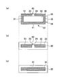
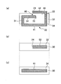
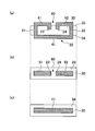
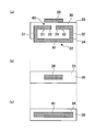
- FIG. 5 to 8 are diagrams showing an example of a stacked arrangement configuration of the capacitive coupling portion.
- a of each figure is a figure which shows an example of the cross section parallel to the lamination direction.
- B) of each figure is a figure which shows an example of a structure by the side of the 1st surface 33 of the base material part 30.
- C) of each figure is a figure which shows an example of the structure by the side of the 2nd surface 34 of the base material part 30.
- the second surface 34 is the surface opposite to the first surface 33.
- the second conductor element 51, the third conductor element 52, and the gap 60 are located on the first surface 33.
- the first conductor element 41 is located on the second surface 34.
- the first tip portion 23 and the second tip portion 24 oppose each other in the longitudinal direction of the second conductor element 51 and the third conductor element 52.
- the gap 60 is formed between the first tip portion 23 and the second tip portion 24 in the longitudinal direction.
- the first conductor element 41 has one end connected to the first outer end portion of the second conductor element 51 via the first via 31 and the second outer end portion of the third conductor element 52. And the other end connected via the second via 32.
- the first via 31 and the second via 32 penetrate the base material portion 30.
- the first tip portion 23 and the second tip portion 24 are in contact with the first surface 33 of the base material portion 30 having a dielectric loss tangent of 0.01 or less.
- the degree of improvement of the radiation efficiency ⁇ with respect to the length obtained by shortening the gap length is increased.
- the third conductor element 52 is located on the first surface 33.
- the second conductor element 51 and the gap 60 are located inside the base material portion 30.
- the first conductor element 41 is located on the second surface 34.
- the first tip portion 23 and the second tip portion 24 oppose each other in the element width direction of the second conductor element 51 and the third conductor element 52.
- the gap 60 is formed between the first tip portion 23 and the second tip portion 24 in the element width direction.
- the first tip 23 is bent at a right angle with respect to the longitudinal direction of the second conductor element 51, and the second tip 24 is at a right angle with respect to the longitudinal direction of the third conductor element 52. Bend.
- the gap 60 has a portion located on the first surface 33 of the base material portion 30 and a portion located inside the base material portion 30.
- the fourth conductor element 26 is capacitively coupled to the second conductor element 51 and the third conductor element 52 via the gap 60. As in the case of FIG. 4, three gaps 60 are formed. Each gap 60 is located inside the base material portion 30.
- the radiation efficiency ⁇ is improved with respect to the length of the gap 60 shortened.
- the degree increases.
- FIG. 9 is a diagram showing an example of the configuration of the antenna 25 during simulation in plan view.
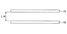
- FIG. 10 is a diagram illustrating an example of a laminated configuration during simulation of the antenna 25.
- the feeding element 21 and the ground 14 are disposed on the feeding element layer 16, and the radiating element 22 and the base material portion 30 are disposed on the radiating element layer 15.
- FIG. 11 is a diagram illustrating an example of a configuration of the radiating element 22 and the power feeding element 21 during simulation.
- the gap on the horizontal axis represents the gap length of the gap 60 between the first tip portion 23 and the second tip portion 24.
- the resonance frequency on the vertical axis represents the resonance frequency of the antenna 25. As shown in FIG. 12, even if the dielectric loss tangent is changed from 0.0001 to 0.1, the resonance frequency hardly changes if the gap length is the same.
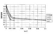
- FIG. 13 is a diagram illustrating an example of the relationship between the dielectric loss tangent and the radiation efficiency ⁇ due to the difference in gap length of the gap 60.
- FIG. 13 shows four cases in which the gap length gap is 0.05 mm, 0.1 mm, 0.5 mm, and 1 mm.
- a portion that is not plotted indicates a region where the antenna 25 does not function as an antenna.
- FIG. 14 is a cross-sectional view schematically showing an example of the configuration of the antenna 25 mounted on a prototype of an actual electronic device.
- the ground 114 is a specific example of the ground 14, the power feeding element 121 is a specific example of the power feeding element 21, and the radiation element 122 is a specific example of the radiation element 22.
- the substrate 113 is an FR4 substrate that is a specific example of the substrate 13.
- the end 112 is a specific example of the end 12 (feeding point).
- the film 130 is a specific example of the base material portion 30 having a dielectric loss tangent greater than 0 and 0.01 or less.
- the radiating element 122 is attached to the inner surface of the glass plate 118 through the film 130.
- the glass plate 118 is a back cover of the electronic device.
- the substrate 113 is attached to a metal casing 117 of the electronic device by at least one attachment portion 119.
- the ground 114 is grounded to the housing 117 via at least one connection part 120.
- the radiating element 122 is an open loop resonant antenna having a gap 60.
- the conductor strip 126 is a specific example of the fourth conductor element 26 described above. In FIG. 14, the conductor strip 126 is not shown.
- the conductor strip 126 is disposed to face the gap 60 through the film 130 so as to be capacitively coupled to the conductor elements on both sides forming the gap 60. That is, the open-loop resonant antenna (radiating element 122) has a structure that can be capacitively coupled to the conductor strip 126 in a direction perpendicular to the film 130.
- the conductor strip 126 is provided between the inner surface of the glass plate 118 and the film 130, and is in contact with both the inner surface of the glass plate 118 and the film 130.
- the radiating element 122 is located on the opposite side of the glass plate 118 with respect to the film 130 so as to be separated from the glass plate 118. .
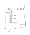
- FIG. 16 is a plan view showing the part shown in FIG. 15 from the viewpoint from the conductor strip 126 side with respect to the film 130.
- the illustration of the glass plate 118 is omitted. Both end portions of the conductor strip 126 are opposed to the conductor elements on both sides forming the gap 60 through the film 130.
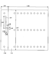
- FIG. 17 is a diagram showing the antenna 25 shown in FIG. 14 in plan view.
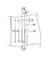
- FIG. 18 is a diagram showing the radiating element 122 and the conductor strip 126 of the antenna 25 shown in FIG. 17 in plan view.
- FIG. 19 is a diagram showing the feeding element 121 of the antenna 25 shown in FIG. 17 in plan view.
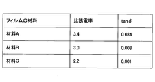
- FIG. 20 is a diagram showing the relative dielectric constant and dielectric loss tangent (tan ⁇ ) of each material.
- FIG. 21 is a diagram illustrating an example of a result of actual measurement of total efficiency due to a difference in material of the film 130.
- FIG. 22 is a diagram illustrating an example of a result of actual measurement of the reflection coefficient S11 due to a difference in material of the film 130.
- the total efficiency represents the product of the radiation efficiency ⁇ and the reflection coefficient S11. That is, the total efficiency represents the radiation efficiency with the return loss of the antenna 25 taken into account.
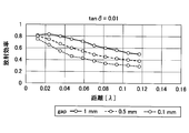
- FIG. 23 is a diagram illustrating an example of a result of calculation on the simulation of the relationship between the distance between the feeding element 21 and the radiating element 22 and the radiation efficiency in the configuration of the antenna 25 illustrated in FIGS. 9 to 11.
- FIG. 23 shows a case where tan ⁇ is 0.01.
- the horizontal axis represents the shortest distance D between the feeding element 21 and the radiating element 22.
- the vertical axis represents the radiation efficiency ⁇ .
- gap represents the gap length of the gap 60 between the first tip portion 23 and the second tip portion 24.
- ⁇ represents the wavelength of the radio wave transmitted or received by the antenna 25.
- the radiation efficiency ⁇ is 50% or more when the gap length is 1 mm.
- the radiation efficiency ⁇ is less than 50%, but by changing tan ⁇ to a value smaller than 0.01, the radiation efficiency ⁇ should be 50% or more. Can do.
- the antenna has been described in the embodiment, but the present invention is not limited to the above embodiment.
- Various modifications and improvements such as combinations and substitutions with some or all of the other embodiments are possible within the scope of the present invention.
Landscapes
- Engineering & Computer Science (AREA)
- Computer Networks & Wireless Communication (AREA)
- Details Of Aerials (AREA)
- Support Of Aerials (AREA)
- Aerials With Secondary Devices (AREA)
Abstract
L'invention concerne une antenne qui est équipée d'un plan de masse, d'un premier résonateur connecté à un point d'alimentation en énergie ayant le plan de masse comme référence, et d'un second résonateur auquel de l'énergie est fournie par le premier résonateur par le biais d'un couplage par champ électromagnétique dans un état sans contact. Le second résonateur comprend une première partie conductrice et une seconde partie conductrice couplée de manière capacitive à la première partie conductrice par l'intermédiaire d'un espace. La tangente de l'angle de pertes de la partie de base sur laquelle le second résonateur est formé est supérieure à 0 mais ne dépasse pas 0,01.
Priority Applications (3)
| Application Number | Priority Date | Filing Date | Title |
|---|---|---|---|
| JP2018512078A JP6891878B2 (ja) | 2016-04-15 | 2017-04-13 | アンテナ |
| CN201780023586.5A CN109075450B (zh) | 2016-04-15 | 2017-04-13 | 天线 |
| US16/157,539 US10931017B2 (en) | 2016-04-15 | 2018-10-11 | Antenna |
Applications Claiming Priority (2)
| Application Number | Priority Date | Filing Date | Title |
|---|---|---|---|
| JP2016-081706 | 2016-04-15 | ||
| JP2016081706 | 2016-04-15 |
Related Child Applications (1)
| Application Number | Title | Priority Date | Filing Date |
|---|---|---|---|
| US16/157,539 Continuation US10931017B2 (en) | 2016-04-15 | 2018-10-11 | Antenna |
Publications (1)
| Publication Number | Publication Date |
|---|---|
| WO2017179676A1 true WO2017179676A1 (fr) | 2017-10-19 |
Family
ID=60042682
Family Applications (1)
| Application Number | Title | Priority Date | Filing Date |
|---|---|---|---|
| PCT/JP2017/015201 Ceased WO2017179676A1 (fr) | 2016-04-15 | 2017-04-13 | Antenne |
Country Status (4)
| Country | Link |
|---|---|
| US (1) | US10931017B2 (fr) |
| JP (1) | JP6891878B2 (fr) |
| CN (1) | CN109075450B (fr) |
| WO (1) | WO2017179676A1 (fr) |
Cited By (2)
| Publication number | Priority date | Publication date | Assignee | Title |
|---|---|---|---|---|
| CN112597707A (zh) * | 2020-10-28 | 2021-04-02 | 中国电子科技集团公司第五十四研究所 | 一种双反射面天线的流固电磁三场耦合计算方法 |
| JPWO2023175646A1 (fr) * | 2022-03-14 | 2023-09-21 |
Families Citing this family (7)
| Publication number | Priority date | Publication date | Assignee | Title |
|---|---|---|---|---|
| WO2018198981A1 (fr) * | 2017-04-27 | 2018-11-01 | Agc株式会社 | Antenne et antenne mimo |
| BR112020018429A2 (pt) | 2018-03-16 | 2020-12-29 | AGC Inc. | Unidade de antena, vidro de janela fixado à unidade de antena e corpo de correspondência |
| FR3094142B1 (fr) * | 2019-03-19 | 2022-04-01 | Sigfox | antenne directive compacte, dispositif comportant une telle antenne |
| KR102708751B1 (ko) | 2019-08-07 | 2024-09-23 | 삼성전자 주식회사 | 안테나를 포함하는 전자 장치 |
| WO2021074969A1 (fr) * | 2019-10-15 | 2021-04-22 | 富士通コネクテッドテクノロジーズ株式会社 | Dispositif d'antenne et dispositif de communication sans fil |
| JP6984951B2 (ja) * | 2020-04-22 | 2021-12-22 | Necプラットフォームズ株式会社 | アンテナ装置及び無線通信装置 |
| JP2025069696A (ja) * | 2023-10-18 | 2025-05-01 | キヤノン株式会社 | 伝送装置及び伝送システム |
Citations (5)
| Publication number | Priority date | Publication date | Assignee | Title |
|---|---|---|---|---|
| JP2011103630A (ja) * | 2009-11-12 | 2011-05-26 | Samsung Electronics Co Ltd | アンテナ装置、及びこれを有する無線通信装置 |
| JP2014103660A (ja) * | 2012-10-24 | 2014-06-05 | Nippon Soken Inc | アンテナ |
| JP2014187720A (ja) * | 2012-07-20 | 2014-10-02 | Asahi Glass Co Ltd | アンテナ装置及びそれを備える無線装置 |
| JP2015220738A (ja) * | 2014-05-21 | 2015-12-07 | 株式会社日本自動車部品総合研究所 | アンテナ装置 |
| WO2016148274A1 (fr) * | 2015-03-19 | 2016-09-22 | 日本電気株式会社 | Antenne et dispositif de communication sans fil |
Family Cites Families (5)
| Publication number | Priority date | Publication date | Assignee | Title |
|---|---|---|---|---|
| EP2143167A4 (fr) * | 2007-05-02 | 2013-05-15 | Nokia Corp | Système d'antenne |
| US20110109525A1 (en) | 2009-11-12 | 2011-05-12 | Samsung Electronics Co., Ltd. | Antenna device and wireless communication apparatus having the same |
| JP6232946B2 (ja) * | 2013-11-07 | 2017-11-22 | 富士通株式会社 | 平面アンテナ |
| JP5666729B1 (ja) * | 2014-03-19 | 2015-02-12 | 学校法人智香寺学園 | 小型アンテナ |
| US10367248B2 (en) * | 2014-03-31 | 2019-07-30 | Nec Corporation | Antenna, array antenna, and radio communication apparatus |
-
2017
- 2017-04-13 WO PCT/JP2017/015201 patent/WO2017179676A1/fr not_active Ceased
- 2017-04-13 JP JP2018512078A patent/JP6891878B2/ja active Active
- 2017-04-13 CN CN201780023586.5A patent/CN109075450B/zh active Active
-
2018
- 2018-10-11 US US16/157,539 patent/US10931017B2/en active Active
Patent Citations (5)
| Publication number | Priority date | Publication date | Assignee | Title |
|---|---|---|---|---|
| JP2011103630A (ja) * | 2009-11-12 | 2011-05-26 | Samsung Electronics Co Ltd | アンテナ装置、及びこれを有する無線通信装置 |
| JP2014187720A (ja) * | 2012-07-20 | 2014-10-02 | Asahi Glass Co Ltd | アンテナ装置及びそれを備える無線装置 |
| JP2014103660A (ja) * | 2012-10-24 | 2014-06-05 | Nippon Soken Inc | アンテナ |
| JP2015220738A (ja) * | 2014-05-21 | 2015-12-07 | 株式会社日本自動車部品総合研究所 | アンテナ装置 |
| WO2016148274A1 (fr) * | 2015-03-19 | 2016-09-22 | 日本電気株式会社 | Antenne et dispositif de communication sans fil |
Cited By (5)
| Publication number | Priority date | Publication date | Assignee | Title |
|---|---|---|---|---|
| CN112597707A (zh) * | 2020-10-28 | 2021-04-02 | 中国电子科技集团公司第五十四研究所 | 一种双反射面天线的流固电磁三场耦合计算方法 |
| CN112597707B (zh) * | 2020-10-28 | 2022-03-01 | 中国电子科技集团公司第五十四研究所 | 一种双反射面天线的流固电磁三场耦合计算方法 |
| JPWO2023175646A1 (fr) * | 2022-03-14 | 2023-09-21 | ||
| WO2023175646A1 (fr) * | 2022-03-14 | 2023-09-21 | 三菱電機株式会社 | Dispositif d'antenne |
| JP7466805B2 (ja) | 2022-03-14 | 2024-04-12 | 三菱電機株式会社 | アンテナ装置 |
Also Published As
| Publication number | Publication date |
|---|---|
| JP6891878B2 (ja) | 2021-06-18 |
| US20190044239A1 (en) | 2019-02-07 |
| CN109075450A (zh) | 2018-12-21 |
| CN109075450B (zh) | 2021-08-27 |
| JPWO2017179676A1 (ja) | 2019-02-21 |
| US10931017B2 (en) | 2021-02-23 |
Similar Documents
| Publication | Publication Date | Title |
|---|---|---|
| JP6891878B2 (ja) | アンテナ | |
| TWI425713B (zh) | 諧振產生之三頻段天線 | |
| CN110544815B (zh) | 电子设备宽带天线 | |
| CN106415929B (zh) | 多天线以及具备该多天线的无线装置 | |
| JP6927293B2 (ja) | アンテナ及びmimoアンテナ | |
| CN101611517B (zh) | 天线 | |
| JP5482171B2 (ja) | アンテナ装置、及び無線端末装置 | |
| TW201433000A (zh) | 天線組件及具有該天線組件的無線通訊裝置 | |
| JP2008124617A (ja) | アンテナ | |
| CN103943942B (zh) | 天线及具有所述天线的便携式设备 | |
| JP2011035440A (ja) | アンテナとそれを有する通信装置 | |
| TW201442347A (zh) | 無線通訊裝置 | |
| JP6478510B2 (ja) | アンテナ | |
| US9300037B2 (en) | Antenna device and antenna mounting method | |
| US9306274B2 (en) | Antenna device and antenna mounting method | |
| JP6233319B2 (ja) | マルチバンドアンテナ及び無線装置 | |
| JP2003152430A (ja) | 二周波共用平板アンテナおよびそれを用いた電気機器 | |
| WO2017179654A1 (fr) | Antenne | |
| CN102157794A (zh) | 谐振产生的三频段天线 | |
| US20080129611A1 (en) | Antenna module and electronic device using the same | |
| CN1964132B (zh) | 使用于可携式装置的隐藏式多频天线 | |
| EP3937309B1 (fr) | Système d'antenne avec région couplée | |
| CN119944286A (zh) | 天线组件及电子设备 | |
| TWM648218U (zh) | 微型天線裝置 | |
| CN119029543A (zh) | 天线组件及可折叠的电子设备 |
Legal Events
| Date | Code | Title | Description |
|---|---|---|---|
| ENP | Entry into the national phase |
Ref document number: 2018512078 Country of ref document: JP Kind code of ref document: A |
|
| NENP | Non-entry into the national phase |
Ref country code: DE |
|
| 121 | Ep: the epo has been informed by wipo that ep was designated in this application |
Ref document number: 17782489 Country of ref document: EP Kind code of ref document: A1 |
|
| 122 | Ep: pct application non-entry in european phase |
Ref document number: 17782489 Country of ref document: EP Kind code of ref document: A1 |