WO2017183222A1 - Dispositif à semi-conducteur et son procédé de fabrication - Google Patents
Dispositif à semi-conducteur et son procédé de fabrication Download PDFInfo
- Publication number
- WO2017183222A1 WO2017183222A1 PCT/JP2016/082199 JP2016082199W WO2017183222A1 WO 2017183222 A1 WO2017183222 A1 WO 2017183222A1 JP 2016082199 W JP2016082199 W JP 2016082199W WO 2017183222 A1 WO2017183222 A1 WO 2017183222A1
- Authority
- WO
- WIPO (PCT)
- Prior art keywords
- semiconductor element
- semiconductor device
- conductive plate
- semiconductor
- insulating substrate
- Prior art date
- Legal status (The legal status is an assumption and is not a legal conclusion. Google has not performed a legal analysis and makes no representation as to the accuracy of the status listed.)
- Ceased
Links
Images


Classifications
-
- H—ELECTRICITY
- H10—SEMICONDUCTOR DEVICES; ELECTRIC SOLID-STATE DEVICES NOT OTHERWISE PROVIDED FOR
- H10W—GENERIC PACKAGES, INTERCONNECTIONS, CONNECTORS OR OTHER CONSTRUCTIONAL DETAILS OF DEVICES COVERED BY CLASS H10
- H10W40/00—Arrangements for thermal protection or thermal control
- H10W40/10—Arrangements for heating
-
- H—ELECTRICITY
- H10—SEMICONDUCTOR DEVICES; ELECTRIC SOLID-STATE DEVICES NOT OTHERWISE PROVIDED FOR
- H10W—GENERIC PACKAGES, INTERCONNECTIONS, CONNECTORS OR OTHER CONSTRUCTIONAL DETAILS OF DEVICES COVERED BY CLASS H10
- H10W40/00—Arrangements for thermal protection or thermal control
- H10W40/20—Arrangements for cooling
- H10W40/25—Arrangements for cooling characterised by their materials
- H10W40/255—Arrangements for cooling characterised by their materials having a laminate or multilayered structure, e.g. direct bond copper [DBC] ceramic substrates
-
- H—ELECTRICITY
- H10—SEMICONDUCTOR DEVICES; ELECTRIC SOLID-STATE DEVICES NOT OTHERWISE PROVIDED FOR
- H10W—GENERIC PACKAGES, INTERCONNECTIONS, CONNECTORS OR OTHER CONSTRUCTIONAL DETAILS OF DEVICES COVERED BY CLASS H10
- H10W40/00—Arrangements for thermal protection or thermal control
- H10W40/20—Arrangements for cooling
- H10W40/25—Arrangements for cooling characterised by their materials
- H10W40/258—Metallic materials
-
- H—ELECTRICITY
- H10—SEMICONDUCTOR DEVICES; ELECTRIC SOLID-STATE DEVICES NOT OTHERWISE PROVIDED FOR
- H10W—GENERIC PACKAGES, INTERCONNECTIONS, CONNECTORS OR OTHER CONSTRUCTIONAL DETAILS OF DEVICES COVERED BY CLASS H10
- H10W40/00—Arrangements for thermal protection or thermal control
- H10W40/60—Securing means for detachable heating or cooling arrangements, e.g. clamps
-
- H—ELECTRICITY
- H10—SEMICONDUCTOR DEVICES; ELECTRIC SOLID-STATE DEVICES NOT OTHERWISE PROVIDED FOR
- H10W—GENERIC PACKAGES, INTERCONNECTIONS, CONNECTORS OR OTHER CONSTRUCTIONAL DETAILS OF DEVICES COVERED BY CLASS H10
- H10W72/00—Interconnections or connectors in packages
- H10W72/071—Connecting or disconnecting
-
- H—ELECTRICITY
- H10—SEMICONDUCTOR DEVICES; ELECTRIC SOLID-STATE DEVICES NOT OTHERWISE PROVIDED FOR
- H10W—GENERIC PACKAGES, INTERCONNECTIONS, CONNECTORS OR OTHER CONSTRUCTIONAL DETAILS OF DEVICES COVERED BY CLASS H10
- H10W74/00—Encapsulations, e.g. protective coatings
- H10W74/01—Manufacture or treatment
-
- H—ELECTRICITY
- H10—SEMICONDUCTOR DEVICES; ELECTRIC SOLID-STATE DEVICES NOT OTHERWISE PROVIDED FOR
- H10W—GENERIC PACKAGES, INTERCONNECTIONS, CONNECTORS OR OTHER CONSTRUCTIONAL DETAILS OF DEVICES COVERED BY CLASS H10
- H10W90/00—Package configurations
-
- H—ELECTRICITY
- H10—SEMICONDUCTOR DEVICES; ELECTRIC SOLID-STATE DEVICES NOT OTHERWISE PROVIDED FOR
- H10W—GENERIC PACKAGES, INTERCONNECTIONS, CONNECTORS OR OTHER CONSTRUCTIONAL DETAILS OF DEVICES COVERED BY CLASS H10
- H10W72/00—Interconnections or connectors in packages
- H10W72/851—Dispositions of multiple connectors or interconnections
- H10W72/874—On different surfaces
- H10W72/884—Die-attach connectors and bond wires
-
- H—ELECTRICITY
- H10—SEMICONDUCTOR DEVICES; ELECTRIC SOLID-STATE DEVICES NOT OTHERWISE PROVIDED FOR
- H10W—GENERIC PACKAGES, INTERCONNECTIONS, CONNECTORS OR OTHER CONSTRUCTIONAL DETAILS OF DEVICES COVERED BY CLASS H10
- H10W90/00—Package configurations
- H10W90/701—Package configurations characterised by the relative positions of pads or connectors relative to package parts
- H10W90/731—Package configurations characterised by the relative positions of pads or connectors relative to package parts of die-attach connectors
- H10W90/734—Package configurations characterised by the relative positions of pads or connectors relative to package parts of die-attach connectors between a chip and a stacked insulating package substrate, interposer or RDL
Definitions
- the present invention relates to a semiconductor device and a manufacturing method thereof.
- semiconductor elements based on Si (silicon) or SiC (silicon carbide) are used. Since it is necessary to keep the temperature of the semiconductor element below a predetermined temperature, it is desirable to efficiently dissipate the heat generated from the semiconductor element.
- an insulating ceramic plate having a high thermal conductivity and a conductive plate made of a metal having a high thermal conductivity provided on both surfaces thereof are integrated.
- silicon nitride, aluminum nitride, or alumina is used for the insulating ceramic plate.
- aluminum (including an aluminum alloy; hereinafter the same) or copper (including a copper alloy; hereinafter the same) is used for the conductive plate.
- the semiconductor element is bonded to one surface of the insulating substrate via a sintered metal such as sintered Ag.
- a cooler is joined directly or indirectly to the other surface of the insulating substrate via a joining material such as solder.
- a semiconductor element has also been proposed from the viewpoint of suppressing deformation of the resin that seals the semiconductor device. Such deformation is caused, for example, by a temperature change in the external environment.
- a semiconductor element having a bending strength of 100 MPa or more and 1000 MPa or less is arranged as a stress relaxation member.
- the stress relaxation member in Patent Document 1 is made of a semiconductor element having a bending strength of 100 MPa or more and 1000 MPa or less arranged on the main surface of the insulating substrate.
- a semiconductor device including a stress relaxation member disclosed in Patent Document 1 has a problem in a direct cooling type module in which a cooler and an insulating substrate are directly joined with solder. On the insulating substrate, there is an Ag sintering portion joined to a semiconductor element (for example, a SiC chip).
- a semiconductor element for example, a SiC chip.
- SiC is expected to withstand a higher junction temperature than Si, and a heat cycle in which high temperature / low temperature is repeated is 175 ° C. or higher at the high temperature. When operating in such a heat cycle, cracks may occur in the Ag sinter part.
- the present invention has been made to solve the above problems, and an object thereof is to provide a semiconductor device having high thermal conductivity and excellent workability, and a method for manufacturing the same.
- the semiconductor device includes an insulating plate, an insulating plate having a first conductive plate provided on one surface of the insulating plate, and a second conductive plate provided on the other surface of the insulating plate.
- a substrate is provided.
- the bending strength of the semiconductor element is 700 MPa or more.
- the semiconductor element has a crack growth depth rate of 30% or less of its chip thickness.
- the method of manufacturing a semiconductor device includes: (a) an insulating plate; a first conductive plate provided on one surface of the insulating plate; and a second conductive plate provided on the other surface of the insulating plate.
- a step of providing an insulating substrate having a conductive plate (b) a step of providing a semiconductor element on the first conductive plate via a sintered metal, and (c) a first of the second conductive plate. And a step of bonding the cooling member via the bonding material.
- the thermal stress due to the difference between the linear expansion coefficient of the semiconductor element and the thermal expansion coefficient of the cooling member is absorbed by the semiconductor element. Therefore, while increasing the thermal conductivity, the stress generated in the bonding material is relieved and the workability is excellent.
- the method for manufacturing a semiconductor device according to the present invention contributes to the manufacture of the semiconductor device according to the present invention.
- FIG. 1 is a cross-sectional view showing a structure of a semiconductor device according to a first embodiment; It is sectional drawing which shows the manufacturing process of a semiconductor element in order. It is sectional drawing which shows the manufacturing process of a semiconductor element in order. It is sectional drawing which shows the manufacturing process of a semiconductor element in order. It is sectional drawing which shows the manufacturing process of a semiconductor element in order. It is sectional drawing which shows the process before manufacturing a semiconductor device after manufacturing a semiconductor element. It is a graph which shows the relationship of the lifetime of the die-bonding material with respect to the linear expansion coefficient of an insulated substrate. It is a SAT image which shows the peeling which generate
- FIG. 6 is a cross-sectional view showing a structure of a semiconductor device according to a second embodiment; FIG. FIG. 6 is a cross-sectional view sequentially showing a manufacturing process of a semiconductor device according to a second embodiment; FIG.
- FIG. 6 is a cross-sectional view sequentially showing a manufacturing process of a semiconductor device according to a second embodiment; 6 is a cross-sectional view showing a structure of a semiconductor device according to a second embodiment; FIG. FIG. 6 is a cross-sectional view showing the structure of another semiconductor device according to the second embodiment.
- FIG. 6 is a sectional view showing a structure of a semiconductor device according to a fourth embodiment.
- FIG. 9 is a cross-sectional view sequentially showing manufacturing steps of a semiconductor device according to a fourth embodiment.
- FIG. 9 is a cross-sectional view sequentially showing manufacturing steps of a semiconductor device according to a fourth embodiment.
- FIG. 9 is a cross-sectional view sequentially showing manufacturing steps of a semiconductor device according to a fourth embodiment.
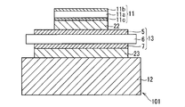
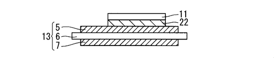
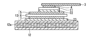
- FIG. 1 is a sectional view showing the structure of the semiconductor device 101 according to the first embodiment.
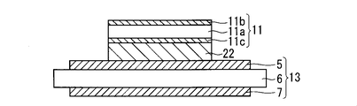
- the semiconductor device 101 includes a semiconductor element 11, a die bond material 22, an insulating substrate 13, a bonding material 23, and a cooling member 12.
- the semiconductor element 11 is bonded to one surface of the insulating substrate 13 via a die bond material 22.
- the other surface of the insulating substrate 13 and the cooling member 12 are bonded via a bonding material 23.
- the insulating substrate 13 includes an insulating ceramic 6 as an insulating plate, a conductive plate 5 provided on one surface of the insulating ceramic 6, and a conductive plate 7 provided on the other surface.
- the insulating substrate 13 includes the conductive plates 5 and 7 and the insulating ceramics 6 disposed between the conductive plate 5 and the conductive plate 7. These are integrated in advance as an insulating substrate 13 using a brazing material or the like.
- the conductive plate 5 is in contact with the die bond material 22. Therefore, the semiconductor element 11 is provided on the conductive plate 5 via the die bonding material 22, and more specifically, bonded to the conductive plate 5.
- the die bonding material 22 may be omitted by bonding the semiconductor element 11 and the insulating substrate 13 by direct bonding such as Cu solid phase diffusion bonding or ultrasonic bonding.
- the guide plate 7 faces the cooling member 12 and is joined to the cooling member 12 via the joining material 23.
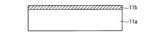
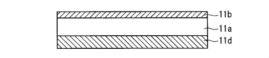
- the semiconductor element 11 has a semiconductor substrate 11a and a wiring electrode 11b electrically connected to the semiconductor substrate 11a.
- the semiconductor element 11 has a back surface (hereinafter referred to as “second main surface”) opposite to the surface (hereinafter referred to as “first main surface”) on which the wiring electrode 11 b is formed (hereinafter referred to as “second main surface”).
- An external output electrode 11c is further provided.
- the semiconductor substrate 11a is made of, for example, SiC.
- SiC is a so-called wide band gap semiconductor.
- a wide bandgap semiconductor has a larger bandgap than Si, and adopting it for the semiconductor substrate 11a is intended to increase the breakdown field strength of the semiconductor element 11 and to keep the semiconductor element 11 at a high temperature of 175 ° C. or higher. This is advantageous from the viewpoint of operation.
- SiC is used as the semiconductor substrate 11a will be described as an example.
- the wiring electrode 11b is realized by any one or a combination of Cu, Al, AlSi, Ni, Au metal layers, for example.
- the back surface external output electrode 11c is realized by any one or a combination of Al, AlSi, Ni, Au metal layers, for example.
- the die bond material 22 for example, a low-temperature sintered material of silver nanoparticles, a liquid phase diffusion bonding material such as Cu—Sn or Ag—Sn, or a bonding material that is a good electrical and thermal conductor such as solder is used. Can do.
- a sintered metal is employed as the die bond material 22 as an example.
- the sintered metal is, for example, sintered Ag.
- the thermal stress generated due to the difference between the thermal expansion coefficient of the semiconductor element 11 and the thermal expansion coefficient of the cooling member 12 during the heat cycle test is absorbed by the semiconductor element 11.
- the die bond material 22 is also bent and stress is generated in the die bond material 22, and the die bond material 22 needs to withstand the stress.
- the thickness of the die bond material 22 is less than 3 ⁇ m, the die bond material 22 cannot withstand the stress generated during the heat cycle test, cracks, and is insufficient in strength. Further, when the die bond material 22 has a thickness exceeding 100 ⁇ m, there is a concern that cracks may occur during the formation process. Therefore, the thickness of the die bond material 22 is preferably 3 ⁇ m or more from the viewpoint of ensuring the strength, and is preferably 100 ⁇ m or less from the viewpoint of preventing the generation of cracks in the formation process.
- a good electrical and thermal conductor such as copper or aluminum can be used.
- the thickness is 0.2 to 1.0 mm and the linear expansion coefficient is 17 ppm.
- the insulating ceramic 6 a ceramic that is an insulator from the electrical viewpoint and that is a good conductor of heat, such as silicon nitride, aluminum nitride, or alumina, can be used.
- silicon nitride is employed for the insulating ceramic 6, for example, the thickness is 0.1 mm to 1.00 mm, and the linear expansion coefficient is 2.5 ppm.
- the overall linear expansion coefficient of the insulating substrate 13 including the conductive plates 5 and 7 can be estimated to be, for example, 5.7 to 8.9 ppm.
- the bonding material 23 for example, a low temperature sintered material of silver nanoparticles, a silver paste material, a liquid phase diffusion bonding material such as Cu-Sn or Ag-Sn, or a bonding material that is a good conductor of heat, such as solder. Can be used.
- solder a bonding material that is a good conductor of heat
- high-strength solder such as Sn—Cu—Sb is preferable.
- the cooling member 12 is formed of a metal material having good heat conduction such as copper or aluminum.
- the thermal resistance from the semiconductor element 11 to the cooling member 12 is small. Therefore, heat generated from the semiconductor element 11 is transmitted to the cooling member 12 with excellent heat transferability. Further, most of the thermal stress resulting from the difference between the thermal expansion coefficient of the semiconductor element 11 and the thermal expansion coefficient of the cooling member 12 is absorbed by the plastic deformation of the semiconductor element 11. Therefore, the reliability of joining between the insulating substrate 13 and the cooling member 12 is sufficiently ensured.
- FIGS. 2 to 5 are cross-sectional views sequentially showing the manufacturing process of the semiconductor element 11.
- a device surface is formed on the first main surface.
- the device surface is, for example, a source side surface in a MOSFET.
- the wiring electrode 11b is formed (see FIG. 2).
- the second main surface is ground so that the thickness of the semiconductor substrate 11a is, for example, 50 ⁇ m or more and 100 ⁇ m or less (see FIG. 3).
- the grinding can be realized, for example, with a grinding machine that employs a grindstone in which diamond abrasive grains are combined by vitrification.
- a protective tape is attached to the first main surface side of the semiconductor substrate 11a to protect the device surface from grinding.
- the device surface may be protected by applying wax or the like to the first main surface and attaching a support substrate.
- a metal film 11d for forming silicide is deposited on the second main surface (see FIG. 4).
- An example of the material of the metal film 11d is Ni.
- the metal film 11d and the semiconductor substrate 11a are reacted to form a silicide layer, thereby forming a contact electrode. This reaction is realized by irradiating the metal film 11d with laser light.
- the surface of the contact electrode is etched to remove the oxide film and the like on the surface. Etching can be realized, for example, by dry etching using Ar + ions. At this time, a part of the unreacted metal film 11d may remain.
- a back external output electrode 11c is formed on the surface of the contact electrode (see FIG. 5).
- the illustration of the contact electrode is omitted.
- the film formation method of the backside external output electrode 11c greatly affects its adhesion.
- the back surface external output electrode 11c is formed by DC sputtering. The film formation temperature became 100 ° C. or higher by the electric power supplied at this time.
- FIGS. 2 to 5 are views focusing on one of the plurality of semiconductor elements 11 manufactured in parallel.
- the semiconductor wafer is used as a semiconductor substrate 11 a in a plurality of semiconductor elements 11.
- a plurality of them are connected via the semiconductor substrate 11a, so that each of the semiconductor elements 11 is obtained by dicing.
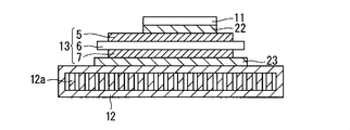
- FIG. 6 is a cross-sectional view showing a process before the semiconductor device 101 is obtained after each of the semiconductor elements 11 is manufactured.
- An insulating substrate 13 in which the conductive plates 5 and 7 and the insulating ceramic 6 are integrated in advance as described above is prepared.
- the semiconductor element 11 is bonded to the conductive plate 5 on the second main surface side through the die bond material 22.
- the cooling member 12 is joined to the conductive plate 7 via the joining material 23.
- the semiconductor device 101 is manufactured (see FIG. 1). That is, this manufacturing process contributes to the manufacture of the semiconductor device 101.
- the semiconductor device 101 bends due to the difference between the linear expansion coefficient of the cooling member 12 that is a good conductor of heat and the linear expansion coefficients of the insulating substrate 13 and the semiconductor element 11. Therefore, the greater the deflection, the greater the stress generated in the die bond material 22.
- the cooling member 12 is directly connected to the bonding material 23 employing, for example, solder.
- the cooling member 12 is bonded to the insulating substrate 13 to which the semiconductor element 11 is die-bonded via the bonding material 23. Therefore, bending due to the difference between the linear expansion coefficient of the cooling member 12 and the linear expansion coefficients of the insulating substrate 13 and the semiconductor element 11 is likely to occur.
- a base plate (not shown) made of a copper material is joined to the cooling member 12 via grease. Further, an insulating substrate 13 to which the semiconductor element 11 is die-bonded is bonded to the base plate through a bonding material employing, for example, solder. Therefore, the bending due to the difference between the linear expansion coefficient of the cooling member 12 and the linear expansion coefficients of the insulating substrate 13 and the semiconductor element 11 is alleviated by the grease and the base plate, and the bending is alleviated compared to the direct cooling type module structure. The That is, the stress generated in the die bond material 22 is reduced.
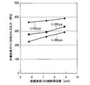
- FIG. 7 is a graph showing the relationship of the lifetime of the die bond material 22 to the overall linear expansion coefficient of the insulating substrate 13 bonded to the semiconductor element 11 via the die bond material 22 in the semiconductor device 101.
- the thickness t of the semiconductor element 11 is adopted as an auxiliary variable in this relationship, and the values are shown as 100 ⁇ m, 200 ⁇ m, and 300 ⁇ m.
- CAE Computer Aided Design
- 7 indicates the linear expansion coefficient of the insulating substrate 13 as a whole (in the drawing, simply expressed as “linear expansion coefficient of the insulating substrate 13”: the same applies hereinafter) in units of ppm. 7 indicates the life of the die bond material 22, that is, the number of cycles of the heat cycle test until the die bond material 22 fails when the heat cycle test is performed.
- the heat cycle test here is a temperature cycle test in which the external environment temperature of the semiconductor device 101 is changed from ⁇ (minus) 40 ° C. to 175 ° C. to ⁇ (minus) 40 ° C. again.
- the linear expansion coefficient is 23 ppm
- the linear expansion coefficient of the semiconductor element 11 using SiC is 4.6 ppm. I will explain to you.
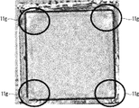
- FIG. 8 is a Scanning Acoustic Tomograph (SAT) image showing the peeling that occurred on the die bond material 22. This peeling is caused by a heat cycle test.
- This SAT image is the semiconductor device 101 viewed from the first main surface side of the semiconductor element 11. In the region 11g of the corner portion of the semiconductor element 11, a white portion indicating a peeled state is visible. Since the depth position of the SAT image is set at the position of the die bond material 22, this portion reflects the peeled state of the die bond material 22. From the viewpoint of improving the number of heat cycles until such peeling of the die bond material 22 occurs, it is desirable to reduce the thickness t of the semiconductor element 11.
- the heat cycle life is about 3000 to 7000 cycles
- the heat cycle life is about 400 to 600 cycles
- the heat cycle life is about 200 to 300 cycles. That is, when the thickness t is 100 ⁇ m, the heat cycle life of the die bond material 22 is improved by about one digit as compared with the case where the thickness t is 200 ⁇ m and 300 ⁇ m. On the other hand, when the thickness t is 200 ⁇ m, the heat cycle life of the die bond material 22 is improved only about twice as compared with the case where the thickness t is 300 ⁇ m.
- the thickness t of the semiconductor element 11 is desirably 100 ⁇ m or less.
- the thickness t is desirably 50 ⁇ m or more. Therefore, it can be said that the desirable range of the thickness t of the semiconductor element 11 is 50 ⁇ m or more and 100 ⁇ m or less (that is, 0.05 mm or more and 0.1 mm or less).
- the semiconductor element 11 In order for the semiconductor element 11 to follow the bending of the cooling member 12, the semiconductor element 11 must withstand the stress applied to itself. Therefore, next, a desirable bending strength range in the semiconductor element 11 will be described.
- the bending strength of the semiconductor element 11 is desirably 700 MPa or more.
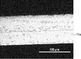
- the bending strength of the semiconductor element 11 depends on the manufacturing process of the semiconductor element 11 and its thickness t. Among them, a dicing condition for the semiconductor element 11 is particularly important. 9 and 10 are both cross-sectional images of the semiconductor element 11 after dicing by a microscope. However, the sample of FIG. 9 and the sample of FIG. 10 have different dicing conditions.
- Fig. 10 no cracks are observed.
- the number of elements that trigger breakage is reduced when the bending strength is evaluated. That is, the workability of the semiconductor device 101 employing the semiconductor element 11 is excellent. Therefore, the sample of FIG. 10 is more preferable than the sample of FIG. 9 from the viewpoint of improving the bending strength.
- the improvement of the dicing conditions can be obtained by appropriately selecting the type and thickness of the blade used for dicing, the type of the dicing tape itself, and the type of the adhesive for the dicing tape.
- the thickness of the blade is desirable to reduce. This is because excessive cracks generated during dicing are reduced. It is also desirable to increase the adhesive strength of the dicing tape adhesive. This is to prevent the object (here, the semiconductor element 11) from being deformed by the stress generated during the blade.
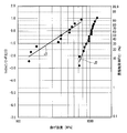
- FIG. 11 is a graph showing the relationship between the cumulative failure rate of the semiconductor element 11 and the bending strength, and shows a so-called Weibull plot.
- the right vertical axis shows the cumulative failure rate F (t) of the semiconductor element 11 as a percentage
- the left vertical axis shows the value ln (ln (1 / (1-F (t)))) (where the symbol ln is the natural logarithm).
- symbol t in symbol F (t) indicates time).
- the horizontal axis of FIG. 11 shows the bending strength of the semiconductor element 11 by adopting MPa as a unit.
- FIG. 11 shows the regression lines J1 and J2 for the semiconductor element 11 manufactured under different first and second dicing conditions.
- the blade thickness is smaller in the second dicing condition than in the first dicing condition, and the adhesive strength of the adhesive of the dicing tape is stronger.
- the semiconductor element 11 manufactured under the first dicing condition has a bending strength of about 100 to 800 MPa as indicated by the regression line J1.
- the semiconductor element 11 manufactured under the second dicing condition has a bending strength of about 700 to 1100 MPa as indicated by the regression line J2.
- the variation in bending strength is smaller in the second dicing condition than in the first dicing condition.
- FIG. 12 is a graph showing stress in the thickness direction (vertical stress) applied to the semiconductor element 11 in the semiconductor device 101.
- the graph shows the result of calculation performed by CAE (Computer Aided Design).
- the value of the stress applied to the semiconductor element 11 is adopted on the vertical axis, and the value of the linear expansion coefficient of the insulating substrate 13 bonded to the semiconductor element 11 via the die bonding material 22 is adopted on the horizontal axis.
- the thickness t of the semiconductor element 11 was used as an auxiliary variable, and 100 ⁇ m, 200 ⁇ m, and 300 ⁇ m were adopted as the value.
- the stress value applied to the semiconductor element 11 is less than 400 MPa at any thickness t of the semiconductor element 11 with respect to the linear expansion coefficient of the insulating substrate 13. Therefore, if the bending strength of the semiconductor element 11 is less than 400 MPa, the semiconductor element 11 is cracked, and if this is 400 MPa or more, it is considered that no defect occurs in the semiconductor element 11.
- the calculation results in FIG. 12 are consistent with the semiconductor element 11 having a bending strength of 700 MPa or more in that there is no defect exemplified by cracking even if the heat cycle test is performed 1000 cycles.
- the thinner the thickness t the higher the stress applied to the semiconductor element 11. That is, the thinner the thickness t, the higher the bending strength of the semiconductor element 11 is required.
- the heat cycle life of the die bond material 22 is improved as the thickness t is decreased.
- the thickness t of the semiconductor element 11 that obtained the cumulative failure rate F (t) related to the graph of FIG. 11 was 100 ⁇ m. Therefore, in consideration of manufacturing variations, the bending strength of the semiconductor element 11 is more preferably 1000 MPa or more.
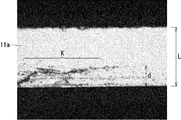
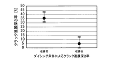
- FIG. 13 is a graph showing the relationship between dicing conditions and crack growth depth rate.
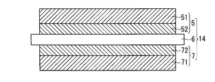
- the crack growth depth ratio indicates the size of a crack entering the chip end face after dicing.
- the crack growth depth rate is defined as a percentage of the ratio of the crack depth d to the chip thickness L (100 ⁇ d / L [%]) with reference to FIG.
- “before improvement” and “after improvement” correspond to the first dicing condition and the second dicing condition, respectively.
- FIG. 13 shows that the crack growth depth rate is lower in the second dicing condition than in the first dicing condition. It can be seen from FIG. 11 that the crack growth depth ratio exceeds 30% under the first dicing condition that caused a decrease in strength. From this, it can be seen that in order to improve the strength, it is necessary to suppress the crack growth depth ratio to 30% or less.
- the semiconductor device 101 absorbs the thermal stress caused by the difference between the linear expansion coefficient of the semiconductor element 11 and the thermal expansion coefficient of the cooling member 12 by the semiconductor element 11. Therefore, the stress generated in the bonding material 23 can be relaxed. Therefore, the semiconductor device 101 having high thermal conductivity and excellent workability and reliability can be obtained. In addition, since the lower limit of the thickness of the semiconductor element 11 does not deteriorate the yield in the manufacturing process of the semiconductor element 11, there is no significant increase in cost.
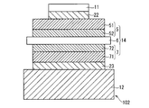
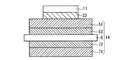
- FIG. 14 is a cross-sectional view showing the structure of the semiconductor device 102 according to this embodiment.
- the semiconductor device 102 has a configuration in which the insulating substrate 13 is replaced with an insulating substrate 14 with respect to the structure of the semiconductor device 101 in the first embodiment.
- Other components are the same as those of the semiconductor device 101.
- the semiconductor element 11 the distinction between the semiconductor substrate 11a, the wiring electrode 11b, and the back surface external output electrode 11c is omitted.
- the insulating substrate 14 includes insulating ceramics 6, copper plates 51 and 71, and aluminum plates 52 and 72.
- the copper plates 51 and 71 are made of copper.
- the aluminum plates 52 and 72 are made of aluminum.
- Aluminum plates 52 and 72 are provided in contact with insulating ceramic 6, copper plate 51 is provided in contact with aluminum plate 52, and copper plate 71 is provided in contact with aluminum plate 72.
- the aluminum plate 52 is sandwiched between the insulating ceramic 6 and the copper plate 51, and the aluminum plate 72 is sandwiched between the insulating ceramic 6 and the copper plate 71.
- the copper plate 51 is bonded to the semiconductor element 11 via the die bond material 22, and the copper plate 71 is bonded to the cooling member 12 via the bonding material 23.
- the copper plate 51 and the aluminum plate 52 can be collectively grasped as the conductive plate 5 according to the first embodiment.
- the copper plate 71 and the aluminum plate 72 can be collectively grasped as the conductive plate 7 according to the first embodiment.
- the conductive plate 7 is made of a laminated structure of copper having high thermal conductivity and aluminum that is easily plastically deformed, so that the insulating substrate 14 and the cooling are compared with the case where the conductive plate 7 is made of only copper.
- the reliability of the joint with the member 12 is improved. This is suitable when the cooling member 12 is made of aluminum. This is because thermal stress is equalized between the members on both sides of the bonding material 23, that is, the cooling member 12 and the conductive plate 7. In particular, when the bonding material 23 is made of solder, the effect is remarkable.
- the aluminum plate 72 is pure aluminum having a purity of at least 99.5% or more, preferably 99.9% or more.
- the linear thermal expansion coefficient of the insulating substrate 14 as a whole can be brought close to the linear thermal expansion coefficient of aluminum, and the stress acting on the bonding material 23 can be reduced.
- Such reduction in stress is desirable from the viewpoint of improving the reliability of bonding between the insulating substrate 14 and the cooling member 12.
- the aluminum plate 52 is also pure aluminum having a purity of at least 99.5% or more, preferably 99.9% or more. It is desirable.
- an insulating substrate 14 is prepared.
- “preparing” refers to preparing an insulating substrate 14 having insulating ceramics 6 as insulating plates and conductive plates 5 and 7 provided on both surfaces of the insulating ceramics 6. Does not mean manufacturing.
- a cooling member 12 is also prepared.
- FIG. 16 shows a step of disposing the semiconductor element 11 on the insulating substrate 14 (more specifically, on the copper plate 51) via the die bonding material 22. Thereafter, the cooling member 12 is further bonded to the copper plate 71 on the opposite side of the insulating substrate 14 from the side on which the semiconductor element 11 is disposed via the bonding material 23, and the configuration shown in FIG. 14 is obtained. It is done.
- FIG. 17 is a cross-sectional view showing the structure of the semiconductor device 103 according to this embodiment.
- the semiconductor device 103 is realized by configuring the backside external output electrode 11c and the conductive plate 5 with copper and omitting the die bonding material 22 from the semiconductor device 101 according to the first embodiment. That is, the back surface external output electrode 11c and the conductive plate 5 are joined to each other without the die bonding material 22 interposed therebetween. Other configurations are the same as those of the semiconductor device 101.
- the back surface external output electrode 11c and the conductive plate 5 are bonded by liquid phase diffusion bonding or solid phase diffusion bonding. Bonding in this manner improves resistance to stress. This improves the reliability of the junction between the insulating substrate 13 and the semiconductor element 11.
- FIG. 18 is a cross-sectional view showing the structure of another semiconductor device 104 according to this embodiment.
- the semiconductor device 104 is realized by configuring the back surface external output electrode 11c from copper and omitting the die bonding material 22 from the semiconductor device 102 according to the second embodiment. That is, the back surface external output electrode 11c and the copper plate 51 are bonded to each other without the die bonding material 22 interposed therebetween.
- Other configurations are the same as those of the semiconductor device 102.
- the back surface external output electrode 11c and the copper plate 51 are bonded by liquid phase diffusion bonding or solid phase diffusion bonding. Bonding in this manner improves resistance to stress. This improves the reliability of the junction between the insulating substrate 14 and the semiconductor element 11.
- the semiconductor element 11 and the insulating substrate 13 or the semiconductor element 11 are insulated.
- the substrate 14 can be bonded by solid phase diffusion bonding or liquid phase diffusion bonding.
- both the back surface external output electrode 11c and the conductive plate 5 are made of copper.
- the conductive plate 7 may also be made of copper.
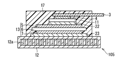
- FIG. 19 is a cross-sectional view showing the structure of the semiconductor device 105 according to this embodiment.
- the semiconductor device 105 has a configuration in which a lead 3, a bonding material 4, and a sealing resin 17 are added to the semiconductor device 101 described in the first embodiment.
- the cooling member 12 has a shape having the radiation fins 12a.
- the semiconductor element 11 the distinction between the semiconductor substrate 11a, the wiring electrode 11b, and the back external output electrode 11c is omitted.
- the bonding material 4 is bonded to the semiconductor element 11 (that is, to the first main surface) on the side opposite to the die bonding material 22, and the lead 3 is bonded to the semiconductor element 11 via the bonding material 4.
- the sealing resin 17 is provided on the cooling member 12 and seals the lead 3, the bonding material 4, the semiconductor element 11, the insulating substrate 13, the die bonding material 22, and the bonding material 23.
- the semiconductor device 105 having such a configuration can be operated at a temperature exceeding 175 ° C. by adopting SiC as the base material of the semiconductor element 11.
- the semiconductor device 105 can be reduced in size, and versatility is increased. For example, when an inverter is configured using the semiconductor device 105, this contributes to downsizing the inverter.
- FIG. 20 to 22 are cross-sectional views sequentially showing the manufacturing process of the semiconductor device 105 according to the present embodiment.
- an insulating substrate 13 in which the conductive plates 5 and 7 and the insulating ceramic 6 are integrated in advance is prepared.
- the 2nd main surface side of the semiconductor element 11 is joined to the conducting plate 5 through the die-bonding material 22 (refer FIG. 20).
- the cooling member 12 is joined to the conductive plate 7 via the joining material 23 (see FIG. 21).
- the bonding material 4 is bonded to the first main surface side of the semiconductor element 11, and the lead 3 is bonded to the bonding material 4 from the side opposite to the semiconductor element 11 with respect to the bonding material 4 (see FIG. 22).
- a sealing resin 17 is provided.
- the manufacturing process shown in FIG. 14 is obtained. In other words, this manufacturing process contributes to the realization of the semiconductor device 105.
- the respective embodiments can be freely combined, arbitrary constituent elements of the respective embodiments are appropriately modified, or arbitrary constituent elements are omitted in the respective embodiments. It is possible to
Landscapes
- Cooling Or The Like Of Semiconductors Or Solid State Devices (AREA)
- Chemical & Material Sciences (AREA)
- Engineering & Computer Science (AREA)
- Materials Engineering (AREA)
- Die Bonding (AREA)
Abstract
Priority Applications (4)
| Application Number | Priority Date | Filing Date | Title |
|---|---|---|---|
| US16/088,532 US10707146B2 (en) | 2016-04-21 | 2016-10-31 | Semiconductor device and method for manufacturing same, for releaved stress and high heat conductivity |
| DE112016006777.1T DE112016006777B4 (de) | 2016-04-21 | 2016-10-31 | Halbleitereinheit und Verfahren zur Herstellung derselben |
| CN201680084542.9A CN109075159B (zh) | 2016-04-21 | 2016-10-31 | 半导体装置及其制造方法 |
| JP2018512772A JP6440903B2 (ja) | 2016-04-21 | 2016-10-31 | 半導体装置およびその製造方法 |
Applications Claiming Priority (2)
| Application Number | Priority Date | Filing Date | Title |
|---|---|---|---|
| JP2016-085068 | 2016-04-21 | ||
| JP2016085068 | 2016-04-21 |
Publications (1)
| Publication Number | Publication Date |
|---|---|
| WO2017183222A1 true WO2017183222A1 (fr) | 2017-10-26 |
Family
ID=60116867
Family Applications (1)
| Application Number | Title | Priority Date | Filing Date |
|---|---|---|---|
| PCT/JP2016/082199 Ceased WO2017183222A1 (fr) | 2016-04-21 | 2016-10-31 | Dispositif à semi-conducteur et son procédé de fabrication |
Country Status (5)
| Country | Link |
|---|---|
| US (1) | US10707146B2 (fr) |
| JP (1) | JP6440903B2 (fr) |
| CN (1) | CN109075159B (fr) |
| DE (1) | DE112016006777B4 (fr) |
| WO (1) | WO2017183222A1 (fr) |
Cited By (3)
| Publication number | Priority date | Publication date | Assignee | Title |
|---|---|---|---|---|
| WO2022059286A1 (fr) * | 2020-09-18 | 2022-03-24 | 株式会社半導体熱研究所 | Élément de liaison pour dispositifs à semi-conducteur |
| WO2022137754A1 (fr) * | 2020-12-23 | 2022-06-30 | 株式会社日立パワーデバイス | Dispositif à semi-conducteur et son procédé de production |
| US20230282620A1 (en) * | 2020-12-02 | 2023-09-07 | Murata Manufacturing Co., Ltd. | Integrated circuit and radio-frequency module |
Families Citing this family (4)
| Publication number | Priority date | Publication date | Assignee | Title |
|---|---|---|---|---|
| US11387213B2 (en) * | 2020-06-05 | 2022-07-12 | Advanced Semiconductor Engineering, Inc. | Method for manufacturing a semiconductor package |
| US12224230B2 (en) * | 2021-09-16 | 2025-02-11 | Amkor Technology Singapore Holding Pte. Ltd. | Semiconductor devices and methods of manufacturing semiconductor devices |
| DE102023110701B3 (de) | 2023-04-26 | 2024-10-02 | Danfoss Silicon Power Gmbh | Befestigung eines Befestigungsobjekts an einem Basisbauteil über einen Zwischenwärmespreizer, der unter Druck auf das Befestigungsobjekt gesintert und mit dem Basisbauteil verlötet wird |
| US20250125231A1 (en) * | 2023-10-17 | 2025-04-17 | Wolfspeed, Inc. | Direct Bonded Semiconductor Die Package |
Citations (6)
| Publication number | Priority date | Publication date | Assignee | Title |
|---|---|---|---|---|
| JP2001230224A (ja) * | 2000-02-14 | 2001-08-24 | Sharp Corp | 半導体装置およびその製造方法 |
| JP2004140179A (ja) * | 2002-10-17 | 2004-05-13 | Toshiba Corp | 半導体装置及びその製造方法 |
| JP2013168431A (ja) * | 2012-02-14 | 2013-08-29 | Mitsubishi Materials Corp | はんだ接合構造、パワーモジュール、ヒートシンク付パワーモジュール用基板及びそれらの製造方法 |
| JP2013207116A (ja) * | 2012-03-28 | 2013-10-07 | Mitsubishi Materials Corp | パワーモジュール、及び、パワーモジュールの製造方法 |
| JP2015015412A (ja) * | 2013-07-08 | 2015-01-22 | 富士電機株式会社 | 半導体装置 |
| JP2015170785A (ja) * | 2014-03-10 | 2015-09-28 | 三菱電機株式会社 | 絶縁基板および電力用半導体装置 |
Family Cites Families (21)
| Publication number | Priority date | Publication date | Assignee | Title |
|---|---|---|---|---|
| DE4233073A1 (de) * | 1992-10-01 | 1994-04-07 | Siemens Ag | Verfahren zum Herstellen eines Halbleiter-Modulaufbaus |
| JP2001222751A (ja) * | 2000-02-14 | 2001-08-17 | Toshiba Electric Appliance Co Ltd | 自動販売機温度制御装置 |
| US7041578B2 (en) * | 2003-07-02 | 2006-05-09 | Texas Instruments Incorporated | Method for reducing stress concentrations on a semiconductor wafer by surface laser treatment including the backside |
| US7619302B2 (en) * | 2006-05-23 | 2009-11-17 | International Rectifier Corporation | Highly efficient both-side-cooled discrete power package, especially basic element for innovative power modules |
| KR20110033117A (ko) * | 2008-06-06 | 2011-03-30 | 미쓰비시 마테리알 가부시키가이샤 | 파워 모듈용 기판, 파워 모듈, 및 파워 모듈용 기판의 제조 방법 |
| JP5526686B2 (ja) * | 2009-09-30 | 2014-06-18 | Dic株式会社 | ジフルオロベンゼン誘導体及びこれを含有する液晶組成物。 |
| US9029200B2 (en) * | 2010-07-15 | 2015-05-12 | Infineon Technologies Austria Ag | Method for manufacturing semiconductor devices having a metallisation layer |
| JP5707885B2 (ja) * | 2010-11-15 | 2015-04-30 | 三菱マテリアル株式会社 | パワーモジュール用基板、冷却器付パワーモジュール用基板、パワーモジュール及びパワーモジュール用基板の製造方法 |
| JP2012197496A (ja) * | 2011-03-22 | 2012-10-18 | Sumitomo Electric Ind Ltd | 複合部材 |
| EP2816593B1 (fr) * | 2012-02-14 | 2020-01-15 | Mitsubishi Materials Corporation | Structure de joint à brasure tendre, module de puissance, substrat fixé au dissipateur de chaleur pour module de puissance, procédé de production dudit substrat et pâte destinée à former une sous-couche de soudure |
| CN104067387B (zh) * | 2012-03-22 | 2016-12-14 | 三菱电机株式会社 | 半导体装置及其制造方法 |
| WO2013161849A1 (fr) * | 2012-04-24 | 2013-10-31 | 株式会社東京精密 | Lame de découpage |
| CN104364884B (zh) * | 2012-06-15 | 2017-06-23 | 株式会社东京精密 | 切割装置以及切割方法 |
| JP2014103182A (ja) | 2012-11-19 | 2014-06-05 | Mitsubishi Electric Corp | 電力用半導体装置 |
| JP6062330B2 (ja) * | 2013-07-16 | 2017-01-18 | カルソニックカンセイ株式会社 | 文字板照明構造 |
| JP6069135B2 (ja) | 2013-08-30 | 2017-02-01 | 株式会社日立製作所 | 電力用半導体装置及びその製造方法、並びに、そのための半田 |
| JP6220657B2 (ja) * | 2013-12-04 | 2017-10-25 | 株式会社Screenホールディングス | 画像記録装置および画像記録方法 |
| CN103922748B (zh) * | 2014-03-14 | 2015-09-16 | 河海大学 | 一种多孔氮化硅陶瓷的制备方法 |
| DE112015000253B4 (de) * | 2014-07-18 | 2023-06-29 | Fuji Electric Co., Ltd. | Halbleitervorrichtung |
| WO2016072517A1 (fr) * | 2014-11-07 | 2016-05-12 | 新日鐵住金株式会社 | Ensemble électro-conducteur pour composant électronique, dispositif à semi-conducteur dans lequel ledit ensemble est utilisé, et procédé de fabrication d'ensemble électro-conducteur |
| CN105140193A (zh) * | 2015-05-04 | 2015-12-09 | 嘉兴斯达半导体股份有限公司 | 一种覆铜陶瓷散热基板的功率模块焊接结构 |
-
2016
- 2016-10-31 CN CN201680084542.9A patent/CN109075159B/zh active Active
- 2016-10-31 US US16/088,532 patent/US10707146B2/en active Active
- 2016-10-31 JP JP2018512772A patent/JP6440903B2/ja active Active
- 2016-10-31 DE DE112016006777.1T patent/DE112016006777B4/de active Active
- 2016-10-31 WO PCT/JP2016/082199 patent/WO2017183222A1/fr not_active Ceased
Patent Citations (6)
| Publication number | Priority date | Publication date | Assignee | Title |
|---|---|---|---|---|
| JP2001230224A (ja) * | 2000-02-14 | 2001-08-24 | Sharp Corp | 半導体装置およびその製造方法 |
| JP2004140179A (ja) * | 2002-10-17 | 2004-05-13 | Toshiba Corp | 半導体装置及びその製造方法 |
| JP2013168431A (ja) * | 2012-02-14 | 2013-08-29 | Mitsubishi Materials Corp | はんだ接合構造、パワーモジュール、ヒートシンク付パワーモジュール用基板及びそれらの製造方法 |
| JP2013207116A (ja) * | 2012-03-28 | 2013-10-07 | Mitsubishi Materials Corp | パワーモジュール、及び、パワーモジュールの製造方法 |
| JP2015015412A (ja) * | 2013-07-08 | 2015-01-22 | 富士電機株式会社 | 半導体装置 |
| JP2015170785A (ja) * | 2014-03-10 | 2015-09-28 | 三菱電機株式会社 | 絶縁基板および電力用半導体装置 |
Cited By (8)
| Publication number | Priority date | Publication date | Assignee | Title |
|---|---|---|---|---|
| WO2022059286A1 (fr) * | 2020-09-18 | 2022-03-24 | 株式会社半導体熱研究所 | Élément de liaison pour dispositifs à semi-conducteur |
| JP2022050871A (ja) * | 2020-09-18 | 2022-03-31 | 株式会社半導体熱研究所 | 半導体デバイスの接合部材 |
| US12119322B2 (en) | 2020-09-18 | 2024-10-15 | Superufo291 Tec | Bonding member for semiconductor device |
| US20230282620A1 (en) * | 2020-12-02 | 2023-09-07 | Murata Manufacturing Co., Ltd. | Integrated circuit and radio-frequency module |
| US12469824B2 (en) * | 2020-12-02 | 2025-11-11 | Murata Manufacturing Co., Ltd. | Integrated circuit and radio-frequency module |
| WO2022137754A1 (fr) * | 2020-12-23 | 2022-06-30 | 株式会社日立パワーデバイス | Dispositif à semi-conducteur et son procédé de production |
| JP2022099858A (ja) * | 2020-12-23 | 2022-07-05 | 株式会社 日立パワーデバイス | 半導体装置およびその製造方法 |
| JP7553194B2 (ja) | 2020-12-23 | 2024-09-18 | ミネベアパワーデバイス株式会社 | 半導体装置およびその製造方法 |
Also Published As
| Publication number | Publication date |
|---|---|
| US20190122955A1 (en) | 2019-04-25 |
| JP6440903B2 (ja) | 2018-12-19 |
| DE112016006777B4 (de) | 2025-08-21 |
| JPWO2017183222A1 (ja) | 2018-08-09 |
| DE112016006777T5 (de) | 2019-01-03 |
| US10707146B2 (en) | 2020-07-07 |
| CN109075159A (zh) | 2018-12-21 |
| CN109075159B (zh) | 2021-12-17 |
Similar Documents
| Publication | Publication Date | Title |
|---|---|---|
| JP6440903B2 (ja) | 半導体装置およびその製造方法 | |
| JP6199397B2 (ja) | 半導体装置およびその製造方法 | |
| US9673163B2 (en) | Semiconductor device with flip chip structure and fabrication method of the semiconductor device | |
| JP6272512B2 (ja) | 半導体装置および半導体装置の製造方法 | |
| JP5542567B2 (ja) | 半導体装置 | |
| JPWO2020116116A1 (ja) | 半導体装置 | |
| CN107611111B (zh) | 半导体模块、电力转换装置 | |
| JP2012253125A (ja) | 半導体装置及び配線基板 | |
| US20130112993A1 (en) | Semiconductor device and wiring substrate | |
| JP2009283741A (ja) | 半導体装置 | |
| JP6643481B2 (ja) | 半導体モジュールおよび半導体モジュールの製造方法 | |
| JP6860334B2 (ja) | 半導体装置 | |
| JP4073876B2 (ja) | 半導体装置 | |
| JP3928488B2 (ja) | 半導体装置およびその製造方法 | |
| JP2014032985A (ja) | 半導体装置およびその製造方法 | |
| JP5368357B2 (ja) | 電極部材およびこれを用いた半導体装置 | |
| JP6129090B2 (ja) | パワーモジュール及びパワーモジュールの製造方法 | |
| JP6259625B2 (ja) | 絶縁基板と冷却器の接合構造体、その製造方法、パワー半導体モジュール、及びその製造方法 | |
| JP6006966B2 (ja) | 半導体装置およびその製造方法 | |
| JP4442609B2 (ja) | 半導体装置およびその製造方法 | |
| JP7495225B2 (ja) | 半導体装置 | |
| TWI395307B (zh) | Semiconductor element module and manufacturing method thereof | |
| JP2014041876A (ja) | 電力用半導体装置 | |
| CN112889148B (zh) | 具有自由浮动封装概念的功率半导体装置 | |
| JP2014143342A (ja) | 半導体モジュール及びその製造方法 |
Legal Events
| Date | Code | Title | Description |
|---|---|---|---|
| ENP | Entry into the national phase |
Ref document number: 2018512772 Country of ref document: JP Kind code of ref document: A |
|
| 121 | Ep: the epo has been informed by wipo that ep was designated in this application |
Ref document number: 16899493 Country of ref document: EP Kind code of ref document: A1 |
|
| 122 | Ep: pct application non-entry in european phase |
Ref document number: 16899493 Country of ref document: EP Kind code of ref document: A1 |
|
| WWG | Wipo information: grant in national office |
Ref document number: 112016006777 Country of ref document: DE |