WO2017183608A1 - Carte de circuit imprimé et son procédé de fabrication - Google Patents
Carte de circuit imprimé et son procédé de fabrication Download PDFInfo
- Publication number
- WO2017183608A1 WO2017183608A1 PCT/JP2017/015467 JP2017015467W WO2017183608A1 WO 2017183608 A1 WO2017183608 A1 WO 2017183608A1 JP 2017015467 W JP2017015467 W JP 2017015467W WO 2017183608 A1 WO2017183608 A1 WO 2017183608A1
- Authority
- WO
- WIPO (PCT)
- Prior art keywords
- thickness
- wiring board
- insulating layer
- conductor
- resin composition
- Prior art date
- Legal status (The legal status is an assumption and is not a legal conclusion. Google has not performed a legal analysis and makes no representation as to the accuracy of the status listed.)
- Ceased
Links
Images
Classifications
-
- H—ELECTRICITY
- H05—ELECTRIC TECHNIQUES NOT OTHERWISE PROVIDED FOR
- H05K—PRINTED CIRCUITS; CASINGS OR CONSTRUCTIONAL DETAILS OF ELECTRIC APPARATUS; MANUFACTURE OF ASSEMBLAGES OF ELECTRICAL COMPONENTS
- H05K1/00—Printed circuits
- H05K1/02—Details
- H05K1/11—Printed elements for providing electric connections to or between printed circuits
- H05K1/118—Printed elements for providing electric connections to or between printed circuits specially for flexible printed circuits, e.g. using folded portions
-
- B—PERFORMING OPERATIONS; TRANSPORTING
- B41—PRINTING; LINING MACHINES; TYPEWRITERS; STAMPS
- B41F—PRINTING MACHINES OR PRESSES
- B41F15/00—Screen printers
- B41F15/14—Details
- B41F15/34—Screens, Frames; Holders therefor
-
- C—CHEMISTRY; METALLURGY
- C08—ORGANIC MACROMOLECULAR COMPOUNDS; THEIR PREPARATION OR CHEMICAL WORKING-UP; COMPOSITIONS BASED THEREON
- C08F—MACROMOLECULAR COMPOUNDS OBTAINED BY REACTIONS ONLY INVOLVING CARBON-TO-CARBON UNSATURATED BONDS
- C08F290/00—Macromolecular compounds obtained by polymerising monomers on to polymers modified by introduction of aliphatic unsaturated end or side groups
- C08F290/02—Macromolecular compounds obtained by polymerising monomers on to polymers modified by introduction of aliphatic unsaturated end or side groups on to polymers modified by introduction of unsaturated end groups
- C08F290/06—Polymers provided for in subclass C08G
-
- C—CHEMISTRY; METALLURGY
- C08—ORGANIC MACROMOLECULAR COMPOUNDS; THEIR PREPARATION OR CHEMICAL WORKING-UP; COMPOSITIONS BASED THEREON
- C08F—MACROMOLECULAR COMPOUNDS OBTAINED BY REACTIONS ONLY INVOLVING CARBON-TO-CARBON UNSATURATED BONDS
- C08F290/00—Macromolecular compounds obtained by polymerising monomers on to polymers modified by introduction of aliphatic unsaturated end or side groups
- C08F290/08—Macromolecular compounds obtained by polymerising monomers on to polymers modified by introduction of aliphatic unsaturated end or side groups on to polymers modified by introduction of unsaturated side groups
- C08F290/14—Polymers provided for in subclass C08G
- C08F290/147—Polyurethanes; Polyureas
-
- H—ELECTRICITY
- H05—ELECTRIC TECHNIQUES NOT OTHERWISE PROVIDED FOR
- H05K—PRINTED CIRCUITS; CASINGS OR CONSTRUCTIONAL DETAILS OF ELECTRIC APPARATUS; MANUFACTURE OF ASSEMBLAGES OF ELECTRICAL COMPONENTS
- H05K1/00—Printed circuits
- H05K1/02—Details
- H05K1/0271—Arrangements for reducing stress or warp in rigid printed circuit boards, e.g. caused by loads, vibrations or differences in thermal expansion
-
- H—ELECTRICITY
- H05—ELECTRIC TECHNIQUES NOT OTHERWISE PROVIDED FOR
- H05K—PRINTED CIRCUITS; CASINGS OR CONSTRUCTIONAL DETAILS OF ELECTRIC APPARATUS; MANUFACTURE OF ASSEMBLAGES OF ELECTRICAL COMPONENTS
- H05K1/00—Printed circuits
- H05K1/02—Details
- H05K1/0277—Bendability or stretchability details
- H05K1/028—Bending or folding regions of flexible printed circuits
-
- H—ELECTRICITY
- H05—ELECTRIC TECHNIQUES NOT OTHERWISE PROVIDED FOR
- H05K—PRINTED CIRCUITS; CASINGS OR CONSTRUCTIONAL DETAILS OF ELECTRIC APPARATUS; MANUFACTURE OF ASSEMBLAGES OF ELECTRICAL COMPONENTS
- H05K1/00—Printed circuits
- H05K1/02—Details
- H05K1/0296—Conductive pattern lay-out details not covered by sub groups H05K1/02 - H05K1/0295
-
- H—ELECTRICITY
- H05—ELECTRIC TECHNIQUES NOT OTHERWISE PROVIDED FOR
- H05K—PRINTED CIRCUITS; CASINGS OR CONSTRUCTIONAL DETAILS OF ELECTRIC APPARATUS; MANUFACTURE OF ASSEMBLAGES OF ELECTRICAL COMPONENTS
- H05K3/00—Apparatus or processes for manufacturing printed circuits
- H05K3/22—Secondary treatment of printed circuits
- H05K3/28—Applying non-metallic protective coatings
- H05K3/285—Permanent coating compositions
- H05K3/287—Photosensitive compositions
-
- B—PERFORMING OPERATIONS; TRANSPORTING
- B41—PRINTING; LINING MACHINES; TYPEWRITERS; STAMPS
- B41M—PRINTING, DUPLICATING, MARKING, OR COPYING PROCESSES; COLOUR PRINTING
- B41M1/00—Inking and printing with a printer's forme
- B41M1/12—Stencil printing; Silk-screen printing
-
- B—PERFORMING OPERATIONS; TRANSPORTING
- B41—PRINTING; LINING MACHINES; TYPEWRITERS; STAMPS
- B41N—PRINTING PLATES OR FOILS; MATERIALS FOR SURFACES USED IN PRINTING MACHINES FOR PRINTING, INKING, DAMPING, OR THE LIKE; PREPARING SUCH SURFACES FOR USE AND CONSERVING THEM
- B41N1/00—Printing plates or foils; Materials therefor
- B41N1/24—Stencils; Stencil materials; Carriers therefor
- B41N1/247—Meshes, gauzes, woven or similar screen materials; Preparation thereof, e.g. by plasma treatment
-
- C—CHEMISTRY; METALLURGY
- C08—ORGANIC MACROMOLECULAR COMPOUNDS; THEIR PREPARATION OR CHEMICAL WORKING-UP; COMPOSITIONS BASED THEREON
- C08L—COMPOSITIONS OF MACROMOLECULAR COMPOUNDS
- C08L2203/00—Applications
- C08L2203/20—Applications use in electrical or conductive gadgets
- C08L2203/202—Applications use in electrical or conductive gadgets use in electrical wires or wirecoating
-
- H—ELECTRICITY
- H05—ELECTRIC TECHNIQUES NOT OTHERWISE PROVIDED FOR
- H05K—PRINTED CIRCUITS; CASINGS OR CONSTRUCTIONAL DETAILS OF ELECTRIC APPARATUS; MANUFACTURE OF ASSEMBLAGES OF ELECTRICAL COMPONENTS
- H05K2201/00—Indexing scheme relating to printed circuits covered by H05K1/00
- H05K2201/01—Dielectrics
- H05K2201/0137—Materials
- H05K2201/0154—Polyimide
-
- H—ELECTRICITY
- H05—ELECTRIC TECHNIQUES NOT OTHERWISE PROVIDED FOR
- H05K—PRINTED CIRCUITS; CASINGS OR CONSTRUCTIONAL DETAILS OF ELECTRIC APPARATUS; MANUFACTURE OF ASSEMBLAGES OF ELECTRICAL COMPONENTS
- H05K2201/00—Indexing scheme relating to printed circuits covered by H05K1/00
- H05K2201/01—Dielectrics
- H05K2201/0183—Dielectric layers
- H05K2201/0191—Dielectric layers wherein the thickness of the dielectric plays an important role
-
- H—ELECTRICITY
- H05—ELECTRIC TECHNIQUES NOT OTHERWISE PROVIDED FOR
- H05K—PRINTED CIRCUITS; CASINGS OR CONSTRUCTIONAL DETAILS OF ELECTRIC APPARATUS; MANUFACTURE OF ASSEMBLAGES OF ELECTRICAL COMPONENTS
- H05K2203/00—Indexing scheme relating to apparatus or processes for manufacturing printed circuits covered by H05K3/00
- H05K2203/07—Treatments involving liquids, e.g. plating, rinsing
- H05K2203/0756—Uses of liquids, e.g. rinsing, coating, dissolving
- H05K2203/0759—Forming a polymer layer by liquid coating, e.g. a non-metallic protective coating or an organic bonding layer
Definitions
- the present invention relates to a printed wiring board having an insulating layer on a conductor pattern, and a method for manufacturing the same.
- the surface of the printed wiring board is provided with a solder resist as an insulating layer for covering and protecting the wiring board and maintaining insulation between the wirings.
- a solder resist As the solder resist, a cover lay film, a cover coat ink, or the like is used.
- a printed wiring board including a conductor pattern having a thickness of, for example, 50 ⁇ m or more is used in order to increase power transmission / reception efficiency (for example, see Patent Document 1).
- a wiring board hereinafter referred to as “thick conductor wiring board” having such a thick conductor pattern (hereinafter referred to as “thick conductor wiring”), it is necessary to cover the surface of the wiring board with an insulating protective layer. .
- the cover coat ink used for general flexible printed wiring boards (conductor thickness: about 10-40 ⁇ m) is printed on the thick conductor wiring board
- the insulating layer is covered with an extremely thin part or insulating layer.
- a portion where the conductor is exposed is generated.
- the conductor is easily exposed at an edge portion of the wiring. Therefore, a coverlay film is often used as the insulating protective layer of the thick conductor wiring board.
- a coverlay film is used as an insulating protective layer of a thick conductor wiring board, in the step portion near the side surface of the wiring, there may be a problem of remaining voids between the wiring and the coverlay film (for example, Patent Document 2).
- Patent Document 2 after an insulating resin layer is screen-printed on a thick conductor wiring board, an adhesive sheet made of the same insulating resin material is laminated thereon, thereby exposing the conductor and between the conductor and the insulating layer. It discloses that the problem of voids can be solved.
- JP2015-146358A Japanese Patent Laid-Open No. 2007-288022
- the present invention provides a coating of a resin composition on a printed wiring board having a thick conductor wiring so that an insulating layer is satisfactorily coated on the thick conductor wiring and insulated in the gaps of the thick conductor wiring.
- An object of the present invention is to provide a thick conductor wiring board in which layers are well embedded.
- the present inventors screen-printed a resin composition having a predetermined solution characteristic using a predetermined screen printing plate, thereby forming an insulating layer on the thick conductor wiring board. It has been found that the insulating layer can be satisfactorily embedded in the gap between the conductor patterns with good coating.
- the present invention relates to a printed wiring board provided with a conductor pattern having a thickness of 50 ⁇ m or more on an insulating substrate, and an insulating layer provided on the conductor pattern and between the conductor patterns, and a manufacturing method thereof.
- the printed wiring board of one embodiment is a flexible printed wiring board using a flexible resin substrate as an insulating substrate.
- the insulating substrate may have a flexible part and a rigid part.
- the thickness of the conductor provided on the flexible substrate is preferably 100 ⁇ m or less.
- the thickness of the insulating layer between the conductor patterns is preferably 0.5 to 2 times the conductor thickness.
- the thickness of the insulating layer on the conductor pattern is preferably 0.1 to 1 times, more preferably 0.3 to 0.7 times the conductor thickness at the center and edge of the conductor pattern.
- the thickness of the insulating layer on the edge of the conductor pattern is preferably 0.3 times or more the thickness of the insulating layer on the center of the conductor pattern.
- An insulating layer is formed by printing a resin composition on a conductive pattern and an insulating substrate between conductive patterns by screen printing and then curing the resin composition.
- the resin composition for forming the insulating layer preferably has a viscosity at 25 ° C. of 50 to 300 P and a thixotropic index of 1.1 to 3.5.
- the screen printing plate used for screen printing preferably has a thickness of 2.2 or more times the wire diameter of the yarn.
- Specific examples of the screen printing plate having a cocoon thickness of 2.2 times or more the yarn diameter include a mesh fabric having a structure in which warp yarns are woven into substantially straight weft yarns.
- the thickness of the screen printing plate is preferably 40 to 200 ⁇ m, and is preferably 4.4 times or less of the wire diameter of the yarn.
- the hardness of the squeegee used for screen printing is preferably 55 to 85 °, and the attack angle is preferably 60 to 90 °.
- the resin composition includes, for example, a binder polymer, a solvent, and a filler.
- a filler a spherical organic filler is preferable.
- a urethane polymer is used as the binder polymer.
- the resin composition may contain an epoxy resin.
- the resin composition may contain a compound having a carboxy group and a polymerizable group in the molecule.
- the resin composition may contain a photopolymerization initiator.
- the solid content concentration of the resin composition is preferably about 40 to 70 wt%.
- the thick conductor wiring can be satisfactorily covered with the insulating layer and the insulating layer can be satisfactorily embedded in the gap of the thick conductor wiring only by applying the resin composition, thereby suppressing problems such as electrical shorts. It is possible to improve the productivity of the thick conductor wiring board.
- the printed wiring board of the present invention can be used for various applications such as a wiring board for wireless power feeding.
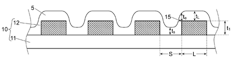
- FIG. 1 is a schematic cross-sectional view showing an embodiment of a printed wiring board, and an insulating resin layer 5 is provided on a wiring board 10 having a conductor pattern 12 on an insulating substrate 11.
- the printed wiring board may be a rigid wiring board using a rigid substrate or a flexible wiring board using a flexible substrate, and may have both a flexible portion and a rigid portion.
- a wiring pattern made of a conductor layer such as copper is provided on a flexible insulating resin substrate such as a polyimide film.
- the thickness of the conductor layer forming the wiring pattern is 10 to 35 ⁇ m, whereas in the thick conductor wiring board used in the present invention, the thickness of the conductor pattern 12 is 50 ⁇ m or more.
- the wiring board 10 including the conductor pattern 12 having a thickness of 50 ⁇ m or more is used.
- the upper limit of the thickness of the conductor pattern 12 is not particularly limited, but is preferably 150 ⁇ m or less, and more preferably 100 ⁇ m or less, from the viewpoint of improving the coverage with the insulating layer 5.
- flexibility can be maintained if the thickness of the conductor pattern is 100 ⁇ m or less.
- the thickness of the conductor pattern is 100 ⁇ m or less in order to maintain flexibility. It is preferable.
- the thickness of the conductor pattern 12 is particularly preferably in the range of about 60 to 80 ⁇ m.
- an insulating resin composition (solder resist ink) is applied by screen printing onto the thick conductor wiring 12 of the thick conductor wiring board 10 and the insulating substrate 11 between the thick conductor wirings, and then cured.
- a printed wiring board can be obtained in which the covering property of the conductor by the insulating layer and the embedding property of the insulating layer between the conductors are secured.
- the resin composition has predetermined solution characteristics (solid content concentration, viscosity and thixotropic index) described later, and the composition is not particularly limited as long as an insulating layer can be formed on the wiring board by screen printing.
- a composition having the same composition as that of a resist ink for general printed wiring boards can be used.
- a thermosetting or photocurable resin composition is preferable.
- the resin composition may be a light / thermosetting composition including both a thermosetting component and a photocurable component.
- the resin composition generally includes a binder polymer and a solvent.
- the binder polymer is not particularly limited as long as it is soluble in the solvent.
- the weight molecular weight of the binder polymer is preferably 1,000 to 1,000,000. When the molecular weight of the binder polymer is in the above range, the solubility in a solvent is excellent, and the viscosity of the resin composition can be adjusted appropriately.
- the weight average molecular weight is determined in terms of polyethylene glycol by gel permeation chromatography (GPC).
- Binder polymers include polyurethane resins, poly (meth) acrylic resins, polyvinyl resins, polystyrene resins, polyethylene resins, polypropylene resins, polyimide resins, polyamide resins, polyacetal resins, polycarbonate resins, polyesters. Resin, polyphenylene ether resin, polyphenylene sulfide resin, polyether sulfone resin, polyether ether ketone resin, and the like.
- the resin composition preferably contains a polyurethane resin as a binder polymer.
- the polyurethane resin is obtained by a reaction between a polyol compound and a polyisocyanate compound.
- long-chain diols such as polyalkylene glycol, polyoxyalkylene diol, polyester diol, polycarbonate diol, and polycaprolactone diol are used, the elastic modulus of the insulating layer obtained by curing of the resin composition decreases, so that the flexibility Tends to improve and warpage decreases.
- the polyisocyanate compound various aromatic polyisocyanate compounds and aliphatic polyisocyanate compounds are used.
- a polymer having a polymerizable group such as a (meth) acryloyl group and a soluble group such as a carboxyl group can be suitably used as the binder polymer.
- the solvent is not particularly limited as long as it can dissolve a resin component such as a binder polymer, and includes sulfoxides, formamides, acetamides, pyrrolidones, acetates, ethers, hexamethylphosphoramide, ⁇ -butyrolactone, and the like.
- a polar organic solvent is preferably used. These polar organic solvents can also be used in combination with aromatic hydrocarbons such as xylene and toluene.
- the amount of solvent in the resin composition may be adjusted so that desired solution characteristics can be obtained. In order to dissolve the resin component and obtain a solution suitable for screen printing, it is preferable to adjust the amount of the solvent so that the solid content concentration of the resin composition is 40 to 70 wt%.
- the thermosetting or photocurable resin composition includes a curable resin component.
- the thermosetting resin composition preferably contains a thermosetting resin component in addition to the binder polymer and the solvent.
- the thermosetting resin component is a compound that generates a crosslinked structure by heating and functions as a thermosetting agent. When the thermosetting resin component generates a crosslinked structure, the heat resistance, chemical resistance and electrical insulation reliability of the insulating layer can be improved.
- the photocurable resin composition contains a radical polymerizable compound and a photopolymerization initiator in addition to the binder polymer and the solvent.
- the photocurable resin composition may further contain a thermosetting resin component or a carboxyl group-containing resin as necessary.
- the photocurable resin composition containing a carboxyl group-containing resin can be used as an alkali development type resist suitable for processing a fine pattern.
- Thermosetting resin component include epoxy resins, bismaleimide resins, bisallyl nadiimide resins, acrylic resins, methacrylic resins, hydrosilyl cured resins, allyl cured resins, unsaturated polyester resins, and the like; Examples thereof include a side chain reactive group type thermosetting polymer having a reactive group such as an allyl group, vinyl group, alkoxysilyl group, hydrosilyl group at the side chain or at the terminal.
- the epoxy resin may be any of a monomer, an oligomer, and a polymer as long as it has at least one epoxy group in the molecule. Among these, a polyfunctional epoxy resin containing two epoxy groups in the molecule is preferable.
- Polyfunctional epoxy resins include bisphenol A type epoxy resin, bisphenol F type epoxy resin, bisphenol S type epoxy resin, hydrogenated bisphenol A type epoxy resin, biphenyl type epoxy resin, phenoxy type epoxy resin, naphthalene type epoxy resin, phenol novolac Type epoxy resin, cresol novolac type epoxy resin, trisphenolmethane type epoxy resin, dicyclopentadiene type epoxy resin, amine type epoxy resin, urethane modified epoxy resin, rubber modified epoxy resin, chelate modified epoxy resin and the like.
- epoxy resin curing agent examples include phenol resins such as phenol novolac resin, cresol novolac resin, naphthalene type phenol resin, amino resin, urea resin, melamine, and dicyandiamide.
- epoxy resin curing accelerators include phosphine compounds, amine compounds, and borate compounds, imidazoles, imidazolines, and azine imidazoles.
- the carboxyl group-containing resin is a compound having at least one carboxyl group in the molecule.
- the carboxyl group-containing resin preferably contains at least one photopolymerizable functional group in the molecule.
- the weight average molecular weight in terms of polyethylene glycol of the carboxyl group-containing compound is preferably 3,000 to 300,000. If the weight average molecular weight is within the above range, an excessive increase in the viscosity of the resin composition is suppressed, and further, the developability, flexibility, and chemical resistance of the photocurable resin composition tend to be improved.
- the acid value of the carboxyl group-containing resin measured by the method defined in JIS K5601-2-1 is preferably 50 to 200 mgKOH / g, more preferably 50 to 150 mgKOH / g.
- an insulating layer having low hygroscopicity, excellent electrical insulation reliability, and excellent developability can be obtained.
- carboxyl group-containing resin examples include a carboxyl group-containing (meth) acrylic copolymer, a carboxyl group-containing vinyl copolymer, acid-modified polyurethane, acid-modified polyester, acid-modified polycarbonate, acid-modified polyamide, and acid-modified polyimide. Is mentioned.
- an acrylic copolymer containing (meth) acrylic acid and (meth) acrylic acid alkyl ester as a copolymerization monomer component is preferable because of excellent photosensitivity, flexibility, and chemical resistance.
- the radical polymerizable compound is a compound that is polymerized by radicals generated by light or heat, and is preferably a compound having at least one unsaturated double bond in the molecule.
- the functional group having an unsaturated double bond is preferably an acrylic group, a methacryloyl group or a vinyl group.
- an EO-modified di (meth) acrylate or a polyfunctional (meth) acrylic compound having three or more (meth) acryloyl groups in one molecule is preferable.
- the number of repeating units of EO (ethylene oxide) contained in one molecule of di (meth) acrylate is preferably 2 to 50, and more preferably 2 to 40.
- an epoxy-modified (meth) acrylic resin in addition to the above, an epoxy-modified (meth) acrylic resin, a urethane-modified (meth) acrylic resin, a polyester-modified (meth) acrylic resin, or the like may be used.
- an epoxy-modified (meth) acrylic resin a urethane-modified (meth) acrylic resin, a polyester-modified (meth) acrylic resin, or the like may be used.
- the photopolymerizable resin composition preferably contains a photopolymerization initiator.
- the photopolymerization initiator is a compound that is activated by light energy such as UV, and initiates and accelerates the photopolymerization reaction such as the above-mentioned radical polymerizable compound, and various known photoradical generators can be appropriately selected and used. Good. It is desirable to use a mixture of two or more photopolymerization initiators.
- the resin composition preferably contains a filler.
- a filler an organic filler, an inorganic filler, an organic-inorganic composite filler, or the like may be appropriately selected and used.
- the organic filler material include poly (meth) acrylic acid alkyl ester, crosslinked poly (meth) acrylic acid alkyl ester, crosslinked styrene, nylon, silicone, crosslinked silicone, and crosslinked urethane.
- Examples of the inorganic filler material include metal oxides such as silica, titanium oxide, and alumina; metal nitrides such as silicon nitride and boron nitride; metal salts such as calcium carbonate, calcium hydrogen phosphate, calcium phosphate, and aluminum phosphate. It is done.
- Examples of the organic-inorganic composite filler include those in which an inorganic layer is formed on the surface of organic fine particles, and those in which an organic layer or organic fine particles are formed on the surface of inorganic fine particles.
- a filler whose surface is modified with a silane coupling agent or the like may be used. From the viewpoint of improving the insulation reliability between the wirings, an organic filler is preferable.
- the shape of the filler includes a spherical shape, a powder shape, a fiber shape, a needle shape, a scale shape, and the like.
- Spherical fillers are preferred because they have no anisotropy and stress is less likely to be unevenly distributed, so that the generation of distortion is suppressed and the warpage of the substrate due to curing shrinkage or the like tends to be reduced.
- spherical organic fillers are preferable from the viewpoint of improving the flexibility of the insulating layer after curing and suppressing warpage of the substrate, and crosslinked urethane beads containing urethane bonds in the molecule are particularly preferable.
- the filler content in the resin composition is 5 to 50 parts by weight with respect to 100 parts by weight of the total solid content.
- the amount is preferably 10 to 40 parts by weight.
- the average particle diameter of the filler is, for example, about 0.01 to 20 ⁇ m. Since a filler having a large particle diameter causes poor insulation, it is preferable to use classified spherical organic beads. Specifically, it is preferable to use a spherical filler having a number ratio of 99.99% or more with a particle diameter of 15 ⁇ m or less.
- the particle diameter can be measured by a laser diffraction / scattering particle diameter distribution measuring apparatus, and the volume-based median diameter is defined as the average particle diameter.
- Resin compositions include photochromic agents, thermochromic inhibitors, plasticizers, dyes, pigments, colorants, antifoaming agents, flame retardants, stabilizers, adhesion-imparting agents, leveling agents, and antioxidants as necessary.
- Various additives such as may be contained.
- Examples of the flame retardant include phosphoric ester compounds, halogen-containing compounds, metal hydroxides, organic phosphorus compounds, and silicones. Among these, phosphorus flame retardants are preferable.
- a resin composition is prepared by mixing the above components. You may grind
- the pulverization / dispersion may be performed using a general kneading apparatus such as a bead mill, a ball mill, or a three roll.
- a method for adding the filler to the resin composition (1) a method in which the resin composition is directly mixed using a stirrer or the like, and (2) addition to the polymerization reaction solution before or during the polymerization of the polymer in the resin composition. (3) A method of mixing with a polymer for a resin composition and other necessary components, and kneading or dispersing by a stress such as a shearing stress such as a three-roll roll or a bead mill. In order to disperse the filler satisfactorily and stabilize the dispersion state, a dispersant, a thickener and the like can also be used.
- the resin composition preferably has a viscosity at 25 ° C. of 50 to 300 poise and a thixotropic index of 1.1 to 3.5.
- the viscosity of the resin composition is a value measured at a rotation speed of 50 rpm using a B-type viscometer.
- the Chixolo topic index is the ratio of the measured viscosity value at 5 rpm and the measured viscosity value at 50 rpm.
- the solution viscosity of the resin composition is more preferably 100 to 300 poise, further preferably 130 to 270 poise, and particularly preferably 150 to 250 poise.
- the thixotropic index of the resin composition is more preferably 1.5 to 3.3, and further preferably 2.0 to 3.2.
- Viscosity and thixotropic properties of the resin composition by controlling the molecular weight of the binder polymer, introducing substituents into the binder polymer, controlling the amount of filler and the particle size of the filler, adding a resin component at room temperature such as a reactive monomer, etc.
- the index can be controlled within the above range.
- the solid content concentration of the resin composition is preferably 40 to 70 wt%, more preferably 45 to 69 wt%, and further preferably 50 to 68 wt%.
- the solid content concentration is a value measured under a drying condition of 170 ° C. ⁇ 1 hour in accordance with JIS K 5601-1-2.
- a resin composition is printed by screen printing on the wiring 12 forming region L of the thick conductor wiring board 10 and the insulating substrate 11 between the conductor patterns S, dried to remove the solvent, and the resin composition is cured as necessary. By doing so, an insulating layer is formed.
- the screen printing method is a method in which printing is performed by scanning a printing squeegee on a screen printing plate on which a resin composition is placed, and transferring the resin composition to a substrate to be printed.
- the resin composition can be applied only to the required area, so that the material use efficiency is high.
- the screen printing method has an advantage of excellent productivity because it is easy to form an insulating layer over a large area, and the throughput is high with a simple process.
- a screen printing plate having a thickness D of 2.2 times or more the yarn wire diameter d is used. Thickness is the thickness of the mesh woven with warp and weft constituting the screen printing plate, and the wire diameter is the diameter of the yarn constituting the mesh. If the mesh has the same woven structure, the thickness D depends on the wire diameter d. The larger the wire diameter, the thicker the thickness and the thicker the printed film thickness.
- the thickness D of the screen printing plate having a general woven structure is about twice the wire diameter d of the yarn.
- the thickness D is approximately twice the yarn diameter d
- the thickness D increases as the yarn diameter d increases.
- the opening becomes smaller, so when printing a resin composition with a large viscosity or thixotropy, the leveling property is insufficient, so the embedding property of the resin composition between the wirings decreases.
- the thickness D is 2.2 times or more the yarn wire diameter d
- the thickness can be increased without reducing the mesh opening, so the printing leveling property of the insulating layer is improved. Therefore, even when the viscosity or thixotropy of the resin composition is large, the wiring on the thick conductor wiring and between the wiring can be satisfactorily covered with the insulating layer.
- the thickness D of the screen printing plate is preferably 0.8 times or more, more preferably 1.0 times or more, and more preferably 1.5 times or more the thickness t 1 of the conductor wiring. preferable.
- the thickness D of the screen printing plate is preferably 3.5 times or less, more preferably 3 or less, and even more preferably 2.8 times or less of the thickness t 1 of the conductor wiring.
- the thickness D of the screen printing plate is preferably 40 to 200 ⁇ m, more preferably 70 to 190 ⁇ m, and further preferably 80 to 180 ⁇ m.
- the thickness D of the screen printing plate is preferably 2.3 to 4.4 times the wire diameter d, more preferably 2.5 to 3.5 times.
- the ShaAtsu of screen printing plate by adjusting the above range, the thickness of the insulating layer on the conductor pattern can be adjusted to 0.1 to 1 times the conductor thickness t 1.
- the thickness of the insulating layer on the conductor pattern is 0.3 to 0.7 times the conductor thickness t 1 is preferred.
- the screen printing plate is formed by knitting a minimum unit of a woven structure from at least one warp and at least one weft, and includes plain weave, twill, plain tatami and twill woven mesh fabrics, etc.
- the structure in which the warp yarn is woven in a substantially straight weft (hereinafter referred to as “thick weave structure”) has a thickness D of more than twice the wire diameter d of the yarn.
- weft yarns stretched with relatively high tension are arranged on the same plane in a straight state without substantially wavy, and warp yarns are greatly waved by stretching warp yarns with relatively low tension. It becomes a hit state and the thickness increases.
- a thick woven screen mesh a thick woven stainless steel mesh (3D-mesh, 3D-165-126) manufactured by Asada Mesh Co., Ltd. is preferably used.
- the weft yarns are alternately shifted in the vertical direction (normal direction of the printing surface). Both warp and weft contact.
- the weft yarn is positioned substantially on the same plane, the warp yarn has a high curvature and undulates up and down, and therefore the weft yarn does not contact the substrate.
- Thick weave printing plates have a small contact area with the substrate, and the resin composition is filled up to the bottom of the screen printing plate (the contact surface with the substrate), so the printed film thickness tends to increase further. It is suitable for printing a resin composition on a thick conductor wiring board.
- the material of the screen printing plate is not particularly limited, and various metal materials such as synthetic fibers such as polyester and nylon, stainless steel, nickel, nickel alloy, titanium, titanium alloy, and copper can be used.
- squeegee used for screen printing those having a squeegee hardness of 55 to 85 ° are particularly preferably used.
- the squeegee hardness is less than 55 °, the pressing force against the substrate to be printed is small, and the embedding property of the insulating layer between the wirings tends to be lowered. If the squeegee hardness is greater than 85 °, the coverage of the insulating layer on the wiring may be reduced.
- the attack angle when the squeegee contacts the screen printing plate is preferably 60 to 90 °.
- the thickness t L of the insulating layer on the thick conductor wiring and the thickness t s of the insulating layer between the wirings (between the conductor patterns) are respectively set to 10 to 100% of the conductor thickness t 1 and 50 It can be controlled to ⁇ 200%.
- the attack angle is smaller than 60 °, the pressing force against the substrate to be printed is small, and the embedding property of the insulating layer between the wirings tends to be lowered.
- the attack angle is larger than 90 °, the discharge amount of the resin composition is decreased, and the coverage of the insulating layer on the wiring may be decreased.
- the insulating film 5 is formed by drying the coating film.
- the drying temperature is preferably 120 ° C. or lower, more preferably 40 to 100 ° C.
- thermosetting is performed after drying.
- a heat-reactive functional group such as an epoxy group by heat treatment
- an insulating layer having excellent heat resistance can be obtained.
- the curing temperature is preferably 100 to 250 ° C, more preferably 120 to 200 ° C, and further preferably 130 to 180 ° C.
- An insulating layer 5 after heat curing is preferably the thickness t L on the wiring is not less than 0.1 times the conductor thickness t 1, the thickness t S between lines than 0.5 times the conductor thickness t 1 Preferably there is.
- Insulating layer 5 after heat curing is preferably the thickness t L on the wiring is less than 1 times the conductor thickness t 1, it is preferable that the thickness t S between the wires is less than 2 times the conductor thickness t 1 . If the thickness of the insulating layer is in the above range, warping of the wiring board due to curing shrinkage of the insulating layer can be suppressed.
- the thickness t S of the insulating layer between the conductor patterns of the wiring board is 0.5 to 2 times the thickness of the conductor thickness t 1 .
- the thickness t S of the insulating layer between the preferred circuit board of the conductor pattern is 0.7 to 1.7 times the conductor thickness t 1, more preferably 0.9 to 1.5 times the conductor thickness t 1 .
- a layer (solder resist) can be formed.
- the thickness t L of the insulating layer on the conductor pattern is preferably 0.3 to 0.7 times the conductor thickness t 1 .
- a thickness t e of the insulating layer 5 on the edge 15 of the conductor pattern is 0.1 to 1 times the conductor thickness t 1 is preferably from 0.3 to 0 0.7 times is more preferable.
- the thickness t e of the insulating layer 5 on the edge 15, or 0.3 times the thickness t L of the center of the insulating layer of the conductor pattern is preferred.
- an insulating layer having a predetermined thickness and excellent coverage can be formed on a thick conductor wiring board by using a resin composition having a predetermined thixotropy and a screen printing plate having a predetermined thickness. .
- ⁇ Formulation Examples 1 to 12 Preparation of resin composition> Binder polymer, epoxy resin, curing accelerator, radical polymerizable polyfunctional acrylate, filler, solvent and other components (photopolymerization initiator, flame retardant, colorant, and antifoaming agent) are shown in Table 1 as formulation example 1. After blending with a composition of ⁇ 12 and mixing with a stirrer equipped with a general stirring blade, the mixture was passed twice with a three-roll mill to obtain a uniform solution.
- a binder polymer (total 82 parts by weight), a curing agent (1 part by weight), a polyfunctional acrylate (total 15 parts by weight), a photopolymerization initiator (total 3.3 parts by weight), a colorant ( The composition of 1.2 parts by weight in total) and the antifoaming agent (2.5 parts by weight) are common, and by changing the type and content of epoxy resin, flame retardant, filler and solvent, the characteristics of the solution ( Solid content concentration and viscosity) were adjusted. In Formulation Example 11, since the solid content concentration was large, it was difficult to prepare the resin composition.
- the particle diameters of the resin compositions of Formulation Examples 1 to 10 were measured with a grindometer, and all were 10 ⁇ m or less. After defoaming the solution with a defoamer, the following evaluation was performed.
- Viscosity and thixotropic index In an environment of 25 ° C., the viscosity of the resin compositions of alignment examples 1 to 10 was measured at a rotation speed of 5 rpm and 50 rpm with a B-type viscometer (Brookfield, rotor No. 4), and the viscosity measured at 5 rpm. The thixotropic index was calculated from the ratio of the viscosity measured at 50 rpm.
- Table 1 shows the composition and solution characteristics (solid content concentration, viscosity (measured value at 50 rpm) and thixotropic index) of Formulation Examples 1-12.
- methyltriglyme is the total amount including the solvent contained in the polymer solution of Synthesis Example 1.
- ⁇ Formation of insulating layer on thick conductor wiring board> Using the above resin composition, a thick conductor with an attack angle of 75 ° using a rubber squeegee with a squeegee hardness of 75 ° (manufactured by Mino Group) using a screen printer (product name “Minomat 5575” manufactured by Mino Group) Screen printing was performed on the wiring board, dried at 80 ° C. for 20 minutes, and then gradually cooled to room temperature. Then, it heat-hardened at 150 degreeC for 30 minutes, and formed the insulating layer in the thick conductor wiring board.
- a flexible wiring board manufactured by Taiyo Kogyo Co., Ltd.
- a rolled copper wiring thickness 70 ⁇ m
- a polyimide film with a thickness of 25 ⁇ m
- Production Examples 1 to 5 the following stainless mesh screen printing plates were used.
- the insulating layer was formed using all the resin compositions of Formulation Examples 1 to 10.
- insulating layers were formed using the resin compositions of Formulation Examples 1 to 5 and Formulation Examples 8 to 10.
- the thickness of the insulating layer on the polyimide substrate on the thick conductor wiring and between the wirings (between the conductor patterns) was measured by cross-sectional microscope observation of the test piece obtained above, and evaluated according to the following criteria.
- the insulating layer thickness is 7 ⁇ m or more and less than 21 ⁇ m (10% or more and less than 30% of the conductor thickness)
- C Insulating layer thickness less than 7 ⁇ m (less than 10% of conductor thickness) (Coverage between wiring)
- C Insulating layer thickness of less than 35 ⁇ m (less than 50% of conductor thickness)
- test piece was cut into an area of 75 mm ⁇ 55 mm around the wiring and placed on a smooth table so that the insulating layer was on the upper surface, and the distance between the table and the end of the test piece was measured.
- Table 2 shows the evaluation results of the coverage and warpage of the insulating layers of the printed wiring boards obtained in Production Examples 1 to 5.
- the resin composition of Formulation Example 8 having a high viscosity, the resin composition of Formulation Example 9 having a low viscosity, and the resin composition of Formulation Example 10 having a high thixotropic index have printability by screen printing. It can be seen that, even when any screen printing plate is used, the insulating layer cannot sufficiently cover the wiring and between the wirings. In the resin compositions of Formulation Examples 1 to 5, in Preparation Example 1 using the screen printing plate having a thickness of 2.1 times the wire diameter, the coverage on the wiring and / or between the wirings was not sufficient. In Production Examples 2 to 5 using the screen printing plate having a thickness of 2.2 times or more of the wire diameter, the coverage with the insulating layer on the wiring and between the wirings was improved.
Landscapes
- Engineering & Computer Science (AREA)
- Microelectronics & Electronic Packaging (AREA)
- Chemical & Material Sciences (AREA)
- Health & Medical Sciences (AREA)
- Chemical Kinetics & Catalysis (AREA)
- Medicinal Chemistry (AREA)
- Polymers & Plastics (AREA)
- Organic Chemistry (AREA)
- Manufacturing & Machinery (AREA)
- Mechanical Engineering (AREA)
- Non-Metallic Protective Coatings For Printed Circuits (AREA)
- Compositions Of Macromolecular Compounds (AREA)
Abstract
La présente invention concerne une carte de circuit imprimé qui comporte des motifs conducteurs (12) pour lesquels l'épaisseur (t1) est d'au moins 50 µm disposés sur un substrat isolé (11), une couche isolante (5) qui est disposée sur un motif conducteur (L) et sur un substrat isolé entre des motifs conducteurs (S). L'épaisseur (tL) de la couche isolante sur les motifs conducteurs est de préférence comprise entre 0,1 et 1 fois l'épaisseur des conducteurs (t1). La couche isolante est formée par impression d'une composition de résine sur les motifs conducteurs et sur le substrat isolé entre des motifs conducteurs par sérigraphie puis durcissement thermique. La composition de résine présente une viscosité comprise entre 50 et 300 P à 25 °C, et un indice de thixotropie compris entre 1,1 et 3,5. La plaque de sérigraphie servant à la sérigraphie présente une épaisseur d'au moins 2,2 fois le diamètre de filetage.
Priority Applications (3)
| Application Number | Priority Date | Filing Date | Title |
|---|---|---|---|
| CN201780024352.2A CN109076705A (zh) | 2016-04-19 | 2017-04-17 | 印刷电路板及其制造方法 |
| US16/090,687 US20200045833A1 (en) | 2016-04-19 | 2017-04-17 | Printed wiring board and method for manufacturing same |
| JP2018513174A JP6955486B2 (ja) | 2016-04-19 | 2017-04-17 | プリント配線板の製造方法 |
Applications Claiming Priority (2)
| Application Number | Priority Date | Filing Date | Title |
|---|---|---|---|
| JP2016-083493 | 2016-04-19 | ||
| JP2016083493 | 2016-04-19 |
Publications (1)
| Publication Number | Publication Date |
|---|---|
| WO2017183608A1 true WO2017183608A1 (fr) | 2017-10-26 |
Family
ID=60116202
Family Applications (1)
| Application Number | Title | Priority Date | Filing Date |
|---|---|---|---|
| PCT/JP2017/015467 Ceased WO2017183608A1 (fr) | 2016-04-19 | 2017-04-17 | Carte de circuit imprimé et son procédé de fabrication |
Country Status (5)
| Country | Link |
|---|---|
| US (1) | US20200045833A1 (fr) |
| JP (1) | JP6955486B2 (fr) |
| CN (1) | CN109076705A (fr) |
| TW (1) | TWI725168B (fr) |
| WO (1) | WO2017183608A1 (fr) |
Cited By (6)
| Publication number | Priority date | Publication date | Assignee | Title |
|---|---|---|---|---|
| JP2017206591A (ja) * | 2016-05-17 | 2017-11-24 | 株式会社カネカ | 熱硬化性樹脂組成物の製造方法及びその利用 |
| JP2019091737A (ja) * | 2017-11-10 | 2019-06-13 | 住友ベークライト株式会社 | 熱硬化性樹脂組成物、回路基板、及び、回路基板の製造方法 |
| JP2020113597A (ja) * | 2019-01-09 | 2020-07-27 | 日立化成株式会社 | 回路基板及びその製造方法、半導体デバイス |
| JP2020115517A (ja) * | 2019-01-17 | 2020-07-30 | 株式会社Screenホールディングス | パターン形成装置、パターン形成方法および吐出データ生成方法 |
| JPWO2022085563A1 (fr) * | 2020-10-23 | 2022-04-28 | ||
| WO2024095812A1 (fr) * | 2022-10-31 | 2024-05-10 | 日本発條株式会社 | Carte de circuit imprimé et module électronique |
Families Citing this family (4)
| Publication number | Priority date | Publication date | Assignee | Title |
|---|---|---|---|---|
| JP7509502B2 (ja) * | 2017-11-28 | 2024-07-02 | 住友電工プリントサーキット株式会社 | フレキシブルプリント配線板の製造方法及びフレキシブルプリント配線板 |
| CN108670561A (zh) * | 2018-05-28 | 2018-10-19 | 宁波市第医院 | 一种显影纱布及其制备方法 |
| KR102311641B1 (ko) | 2018-11-23 | 2021-10-13 | 주식회사 엘지화학 | 수지 조성물, 이를 포함하는 프리프레그, 이를 포함하는 적층판, 및 이를 포함하는 수지 부착 금속박 |
| KR102900575B1 (ko) * | 2020-09-11 | 2025-12-16 | 삼성디스플레이 주식회사 | 인쇄 회로 기판, 표시 장치 및 표시 장치 제조 방법 |
Citations (6)
| Publication number | Priority date | Publication date | Assignee | Title |
|---|---|---|---|---|
| JPH02308163A (ja) * | 1989-05-23 | 1990-12-21 | Hitachi Chem Co Ltd | 感光性樹脂組成物 |
| JPH066016A (ja) * | 1991-11-06 | 1994-01-14 | Nippon Paint Co Ltd | はんだ止めマスクの形成方法 |
| JP2001177200A (ja) * | 1999-12-17 | 2001-06-29 | Toyobo Co Ltd | フレキシブルプリント配線板及びその製造方法 |
| JP2003268649A (ja) * | 2002-03-13 | 2003-09-25 | Nakanuma Art Screen Kk | メッシュ織物及び当該メッシュ織物を使用したスクリーン印刷版 |
| WO2013111478A1 (fr) * | 2012-01-25 | 2013-08-01 | 株式会社カネカ | Nouvelle composition de résine pour film isolant et son utilisation |
| JP2016012002A (ja) * | 2014-06-27 | 2016-01-21 | 日立化成株式会社 | 感光性樹脂組成物の硬化物、それに用いる感光性樹脂組成物及び半導体装置搭載用基板の製造方法、半導体装置の製造方法 |
Family Cites Families (11)
| Publication number | Priority date | Publication date | Assignee | Title |
|---|---|---|---|---|
| US4752553A (en) * | 1982-04-01 | 1988-06-21 | M&T Chemicals Inc. | High resolution solder mask photopolymers for screen coating over circuit traces |
| US4556627A (en) * | 1982-04-01 | 1985-12-03 | Sullivan Donald F | Transferring polymer from thin plastic films to photodevelop insulation patterns on printed wiring boards |
| EP0541111B1 (fr) * | 1991-11-06 | 1997-03-19 | Nippon Paint Co., Ltd. | Procédé de préparation d'un masque pour soudage |
| TW200405786A (en) * | 2002-08-06 | 2004-04-01 | Taiyo Ink Mfg Co Ltd | Manufacturing method of multi-layer printed circuit board and multi-layer printed circuit board |
| KR101581387B1 (ko) * | 2008-06-02 | 2015-12-30 | 가부시키가이샤 가네카 | 신규한 수지 조성물 및 그 이용 |
| JP5755401B2 (ja) * | 2009-04-30 | 2015-07-29 | 株式会社ピーアイ技術研究所 | 変性ポリイミドの製造方法及び変性ポリイミド |
| CN101959372B (zh) * | 2010-05-24 | 2012-03-14 | 大连太平洋多层线路板有限公司 | 一种超厚铜线路板阻焊加工方法 |
| KR101978992B1 (ko) * | 2011-04-28 | 2019-05-16 | 가부시키가이샤 가네카 | 신규한 도전층 일체형 플렉서블 프린트 기판 |
| CN103374307B (zh) * | 2012-04-28 | 2015-01-14 | 富葵精密组件(深圳)有限公司 | 背胶铜箔、其制作方法、多层柔性线路板及其制作方法 |
| US9832902B2 (en) * | 2013-05-31 | 2017-11-28 | Elantas Pdg, Inc. | Formulated resin compositions for flood coating electronic circuit assemblies |
| WO2016017596A1 (fr) * | 2014-07-28 | 2016-02-04 | 日立化成株式会社 | Composition de résine photosensible, élément photosensible, procédé de production d'un motif de réserve et procédé de fabrication d'une carte à circuits imprimés |
-
2017
- 2017-04-17 US US16/090,687 patent/US20200045833A1/en not_active Abandoned
- 2017-04-17 JP JP2018513174A patent/JP6955486B2/ja active Active
- 2017-04-17 WO PCT/JP2017/015467 patent/WO2017183608A1/fr not_active Ceased
- 2017-04-17 CN CN201780024352.2A patent/CN109076705A/zh active Pending
- 2017-04-19 TW TW106113040A patent/TWI725168B/zh active
Patent Citations (6)
| Publication number | Priority date | Publication date | Assignee | Title |
|---|---|---|---|---|
| JPH02308163A (ja) * | 1989-05-23 | 1990-12-21 | Hitachi Chem Co Ltd | 感光性樹脂組成物 |
| JPH066016A (ja) * | 1991-11-06 | 1994-01-14 | Nippon Paint Co Ltd | はんだ止めマスクの形成方法 |
| JP2001177200A (ja) * | 1999-12-17 | 2001-06-29 | Toyobo Co Ltd | フレキシブルプリント配線板及びその製造方法 |
| JP2003268649A (ja) * | 2002-03-13 | 2003-09-25 | Nakanuma Art Screen Kk | メッシュ織物及び当該メッシュ織物を使用したスクリーン印刷版 |
| WO2013111478A1 (fr) * | 2012-01-25 | 2013-08-01 | 株式会社カネカ | Nouvelle composition de résine pour film isolant et son utilisation |
| JP2016012002A (ja) * | 2014-06-27 | 2016-01-21 | 日立化成株式会社 | 感光性樹脂組成物の硬化物、それに用いる感光性樹脂組成物及び半導体装置搭載用基板の製造方法、半導体装置の製造方法 |
Cited By (8)
| Publication number | Priority date | Publication date | Assignee | Title |
|---|---|---|---|---|
| JP2017206591A (ja) * | 2016-05-17 | 2017-11-24 | 株式会社カネカ | 熱硬化性樹脂組成物の製造方法及びその利用 |
| JP2019091737A (ja) * | 2017-11-10 | 2019-06-13 | 住友ベークライト株式会社 | 熱硬化性樹脂組成物、回路基板、及び、回路基板の製造方法 |
| JP2020113597A (ja) * | 2019-01-09 | 2020-07-27 | 日立化成株式会社 | 回路基板及びその製造方法、半導体デバイス |
| JP2020115517A (ja) * | 2019-01-17 | 2020-07-30 | 株式会社Screenホールディングス | パターン形成装置、パターン形成方法および吐出データ生成方法 |
| JP7281907B2 (ja) | 2019-01-17 | 2023-05-26 | 株式会社Screenホールディングス | パターン形成装置、パターン形成方法および吐出データ生成方法 |
| JPWO2022085563A1 (fr) * | 2020-10-23 | 2022-04-28 | ||
| WO2022085563A1 (fr) * | 2020-10-23 | 2022-04-28 | 東亞合成株式会社 | Composition de résine, film de liaison, stratifié avec couche de composition de résine, stratifié et film de protection contre les ondes électromagnétiques |
| WO2024095812A1 (fr) * | 2022-10-31 | 2024-05-10 | 日本発條株式会社 | Carte de circuit imprimé et module électronique |
Also Published As
| Publication number | Publication date |
|---|---|
| CN109076705A (zh) | 2018-12-21 |
| TW201740780A (zh) | 2017-11-16 |
| TWI725168B (zh) | 2021-04-21 |
| JPWO2017183608A1 (ja) | 2019-02-21 |
| US20200045833A1 (en) | 2020-02-06 |
| JP6955486B2 (ja) | 2021-10-27 |
Similar Documents
| Publication | Publication Date | Title |
|---|---|---|
| JP6955486B2 (ja) | プリント配線板の製造方法 | |
| KR102369508B1 (ko) | 경화성 수지 조성물, 드라이 필름, 경화물 및 프린트 배선판 | |
| TWI448510B (zh) | A thermosetting resin composition, a protective film for a flexible circuit substrate, and a surface protective film | |
| KR102023165B1 (ko) | 광경화성 및 열경화성을 갖는 수지 조성물 및 드라이 필름 솔더 레지스트 | |
| CN111742014A (zh) | 层叠型电子部件用树脂组合物、干膜、固化物、层叠型电子部件和印刷电路板 | |
| CN110291152B (zh) | 热固性树脂组合物、其固化物和印刷电路板 | |
| CN111936575A (zh) | 固化性树脂组合物、干膜、固化物和电子部件 | |
| WO2019188344A1 (fr) | Composition de résine durcissable, produit durci associé et carte de circuit imprimé | |
| CN114574017B (zh) | 树脂组合物 | |
| CN108350203B (zh) | 黑色树脂组合物、附带黑色树脂固化膜的聚酰亚胺及其制造方法 | |
| CN108885400A (zh) | 固化性树脂组合物、干膜、固化物和印刷电路板 | |
| KR20140018117A (ko) | 광경화성 및 열경화성을 갖는 수지 조성물과, 드라이 필름 솔더 레지스트 | |
| JP2018173609A (ja) | 硬化性樹脂組成物、ドライフィルム、硬化物およびプリント配線板 | |
| JP7168443B2 (ja) | 硬化性樹脂組成物、ドライフィルム、硬化物、配線板及び電子部品 | |
| KR20240013666A (ko) | 수지 조성물 | |
| JP7371321B2 (ja) | 硬化性樹脂組成物、硬化物、およびプリント配線板 | |
| WO2019189219A1 (fr) | Composition de résine durcissable, film sec, produit durci et carte de circuit imprimée | |
| WO2024181495A1 (fr) | Composition de résine durcissable | |
| JP2017206591A (ja) | 熱硬化性樹脂組成物の製造方法及びその利用 | |
| JP7596648B2 (ja) | 液状組成物及びシート | |
| CN108241253B (zh) | 碱显影型阻焊剂组合物、其干膜、和固化物以及印刷电路板 | |
| JP2024146833A (ja) | 硬化性樹脂組成物および硬化性樹脂組成物を用いたプリント配線基板の製造方法 | |
| KR102857956B1 (ko) | 내열성 및 내환경성이 개선된 접착제 조성물을 포함하는 전기전자용 절연필름의 제조 방법 | |
| TWI920230B (zh) | 液狀組合物、其製造方法及附有凸部之構件 | |
| CN120399396A (zh) | 固化性树脂组合物、固化物、印刷布线板以及其制造方法 |
Legal Events
| Date | Code | Title | Description |
|---|---|---|---|
| ENP | Entry into the national phase |
Ref document number: 2018513174 Country of ref document: JP Kind code of ref document: A |
|
| NENP | Non-entry into the national phase |
Ref country code: DE |
|
| 121 | Ep: the epo has been informed by wipo that ep was designated in this application |
Ref document number: 17785946 Country of ref document: EP Kind code of ref document: A1 |
|
| 122 | Ep: pct application non-entry in european phase |
Ref document number: 17785946 Country of ref document: EP Kind code of ref document: A1 |