WO2017185493A1 - Appareil d'antenne et terminal mobile - Google Patents
Appareil d'antenne et terminal mobile Download PDFInfo
- Publication number
- WO2017185493A1 WO2017185493A1 PCT/CN2016/085550 CN2016085550W WO2017185493A1 WO 2017185493 A1 WO2017185493 A1 WO 2017185493A1 CN 2016085550 W CN2016085550 W CN 2016085550W WO 2017185493 A1 WO2017185493 A1 WO 2017185493A1
- Authority
- WO
- WIPO (PCT)
- Prior art keywords
- antenna device
- slit
- frame
- frame segment
- matching circuit
- Prior art date
- Legal status (The legal status is an assumption and is not a legal conclusion. Google has not performed a legal analysis and makes no representation as to the accuracy of the status listed.)
- Ceased
Links
Images


Classifications
-
- H—ELECTRICITY
- H01—ELECTRIC ELEMENTS
- H01Q—ANTENNAS, i.e. RADIO AERIALS
- H01Q1/00—Details of, or arrangements associated with, antennas
- H01Q1/44—Details of, or arrangements associated with, antennas using equipment having another main function to serve additionally as an antenna, e.g. means for giving an antenna an aesthetic aspect
Definitions
- the present application relates to the field of antenna technologies, and in particular, to an antenna device and a mobile terminal to which the antenna device is applied.
- the design of the metal material is more textured, so the mobile phone with the metal casing gradually occupied the mainstream of the market.
- the appearance of the metal casing broke the design idea of the traditional mobile phone antenna, which greatly increased the difficulty of the antenna design.
- it has been considered to use a metal casing as part of an antenna, and a metal casing is used for signal radiation.
- a metal casing is used for signal radiation.
- more and more frequency bands are applied to mobile phone terminals, which requires good compatibility of mobile phone antennas and can work in multiple frequency bands at the same time.
- the current mobile terminal that uses the metal casing as a part of the antenna cannot effectively widen the frequency band of the antenna, and the problem of insufficient coverage of the antenna bandwidth occurs, and it is difficult to meet the requirements of the communication system.
- the technical problem to be solved by the present application is to provide an antenna device and a mobile terminal, which are used to solve the problem that the bandwidth of the antenna cannot be effectively widened in the prior art, and the coverage of the antenna bandwidth is insufficient.
- an antenna device provided by the present application is applied to a mobile terminal, where the mobile terminal includes a conductive frame, and the conductive frame is provided with a slit and a first frame segment and a second portion on both sides of the slit a frame segment, the antenna device includes a feed point, a first matching circuit, the first frame segment, the second frame segment, a second matching circuit, and a frequency modulation component, wherein the first matching circuit is connected in series to the feed Between the electrical point and the first frame segment, the frequency modulation component and the second matching circuit are sequentially connected in series between the ground and the second frame segment, and the slit is used to implement the first frame segment Electrical coupling with the second frame segment to effect a feed loop from the feed point to ground, the frequency modulation component for adjusting the frequency range of the antenna device.
- the frequency modulation component is a switching component, and the switching of the switching component is used to change the architecture of the antenna device.
- the frequency modulation component is a tunable capacitor for adjusting parameters of the feed loop to change the frequency of the antenna device.
- the frequency modulation component is a tunable inductor for adjusting parameters of the feed loop to change The frequency of the antenna device.
- the slit comprises at least two micro slits arranged side by side.
- the width of the micro slit is less than or equal to 0.5 mm.
- the first frame body and the second frame body are respectively grounded.
- the first frame body and the second frame body are both made of metal.
- the slit is filled with an insulating material.
- the conductive frame is further provided with a first auxiliary slit, and the first frame segment is disposed between the first auxiliary slit and the slit.
- the conductive frame is further provided with a second auxiliary slit, and the second frame segment is disposed between the slit and the second auxiliary slit.
- the present application provides a mobile terminal, where the mobile terminal includes a main board and the antenna device according to any one of the above, the feeding point of the antenna device, the first matching circuit, and the The two matching circuits and the frequency modulation components are all disposed on the main board.
- the beneficial effects of the present application are as follows:
- the present application divides the conductive frame into a first frame and a second frame by slitting, and the first frame and the second frame serve as part of the antenna device, thereby improving the radiation efficiency of the antenna device.
- the frequency modulation component is used to adjust the frequency range of the antenna device, so that the bandwidth covered by the antenna device is broadened, the antenna performance is improved, and the coverage of the antenna bandwidth is increased.
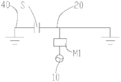
- FIG. 1 is a schematic diagram of an antenna apparatus according to an embodiment of a first embodiment of the present invention.
- FIG. 2 is a schematic diagram showing an equivalent circuit of a switching element of the antenna device shown in FIG. 1 in an on state.
- FIG. 3 is a schematic diagram showing an equivalent circuit of the switching element of the antenna device shown in FIG. 1 in an off state.
- FIG. 4 is a schematic diagram of an antenna apparatus according to another embodiment of the first embodiment of the present invention.
- FIG. 5 is a schematic diagram of an antenna apparatus according to an embodiment of a second embodiment of the present invention.
- FIG. 6 is a schematic diagram showing an equivalent circuit of the antenna device shown in FIG. 5.
- FIG. 7 is a schematic diagram of an antenna apparatus according to another embodiment of a second embodiment of the present invention.
- the present application relates to an antenna device and a mobile terminal, including but not limited to a mobile phone, a palmtop computer, a tablet computer, and the like.
- the antenna device is applied to a mobile terminal.
- the mobile terminal includes a conductive frame.
- the conductive frame is made of a metal material.
- the conductive frame can also be other conductive materials, such as conductive plastic or conductive rubber.
- the main function of the conductive frame is to transmit electrical energy and electrical signals.
- the conductive frame is provided with a slit and a first frame segment and a second frame segment on both sides of the slit, and the slit design can realize a signal radiation path of the antenna inside the mobile terminal, that is, a setting inside the mobile terminal
- the signal of the antenna module can be transmitted to the outside of the mobile terminal through a slit or receive a signal transmitted from outside the mobile terminal.
- the slit design can also provide electrical coupling between the first frame segment and the second frame segment when the first frame segment and the second frame segment are part of the antenna assembly.
- the antenna device of the present application includes a frequency modulation component for adjusting a frequency range of the antenna device.
- the frequency modulation component may be a switching component, a tunable capacitor or a tunable inductor. Details are as follows.
- the frequency modulation element is a switching element.
- the antenna device includes a feeding point 10, a first matching circuit M1, the first frame segment 20, the second frame segment 40, a second matching circuit M2, and a switching element 50.
- a matching circuit M1 is connected in series between the feed point 10 and the first frame segment 20, and the switching element 50 and the second matching circuit M2 are sequentially connected in series between the ground and the second frame segment 40.
- a slit S is used to achieve electrical coupling between the first frame segment 20 and the second frame segment 40 to implement a feed circuit from the feed point 10 to the ground, the switching element 50
- the switching is used to change the architecture of the antenna device, so that the antenna device can be reconstructed so that the antenna device can cover a wider bandwidth and increase the frequency range of the antenna.
- the present application realizes electrical coupling between the first frame segment 20 and the second frame segment 40 by the slit S, that is, the signal transmission and current transmission between the first frame segment 20 and the second frame segment 40 are both passed. Slotted S
- the electrical coupling is implemented, and the slit S is disposed between the first frame segment 20 and the second frame segment 40, which is equivalent to providing a capacitor between the first frame segment 20 and the second frame segment 40.
- the arrangement of the slit S can effectively isolate the first frame 20 and the second frame 40.
- the slit S is isolated so that different signals radiated or received by the antenna device are also isolated, thereby improving the stability of the signal transmission of the antenna and preventing interference between the signals.
- the first frame segment 20 and the second frame segment 40 are respectively grounded, the mobile terminal is provided with a main board, the main board includes a grounding surface, and the first frame segment 20 and the second frame segment 40 are electrically connected to the main board.
- Ground plane Specifically, a grounding spring piece may be disposed at an edge of the main board, connected between the first frame section 20 and the grounding surface of the main board through the grounding elastic piece, and connected between the second frame section 40 and the grounding surface of the main board by the grounding elastic piece.
- the grounding shrapnel can also be replaced by a conductive probe.
- the feeding point 10 When the switching element 50 is in an on state, please refer to FIG. 2, the feeding point 10, the first matching circuit M1, the first frame 20, the second frame 40, the second matching circuit M2, and the ground.
- the series is turned on in series to form a loop antenna structure.
- the switching element 50 When the switching element 50 is in the off state, please refer to FIG. 3, the branch of the second matching circuit M2 is disconnected, and the second matching circuit M2 is not working. At this time, the feeding point 10, the first matching The circuit M1, the first frame 20, the second frame segment 40 and the ground are sequentially connected in series to form an inverted F antenna structure.
- the first matching circuit M1 and the second matching circuit M2 are used to match the impedance of the antenna device to reduce return loss due to impedance mismatch.
- the first matching circuit M1 and the second matching circuit M2 can be implemented by series and/or parallel inductance or capacitance.
- the specific circuit architecture is not limited in this application.
- the switching element 50 is a radio frequency switch, and the switching element 50 can change the length of the radiator of the antenna device to realize the tuning function of the antenna device.
- the slit S comprises at least two micro slits arranged side by side at equal intervals.
- the width of the micro slit is less than or equal to 0.5 mm.
- the slit is designed as an architecture of at least two micro slits, so that the conductive border of the mobile terminal appears to be a whole, and the user experience is improved from an aesthetic point of view.
- the first frame segment 20 and the second frame segment 40 are both made of metal, and the two can be the same
- the material can also be designed as a different material as needed.
- the slit S is filled with an insulating material, and the insulating material may be ceramic or plastic.
- the feeding point 10, the first matching circuit M1, the second matching circuit M2, and the switching element 50 are all disposed on a main board in the mobile terminal.
- the present application divides the conductive frame into the first frame segment 20 and the second frame 40 by the slit S, and the first frame segment 20 and the second frame segment 40 serve as part of the antenna device, thereby improving the radiation efficiency of the antenna device, and
- the switching of the switching element 50 is used to change the architecture of the antenna device, so that the reconstruction of the antenna device can be realized, so that the antenna device can cover a wider bandwidth, and the frequency range of the antenna can be increased to realize the reconstruction of the antenna device.
- the bandwidth covered by the antenna device is broadened, the antenna performance is improved, and the coverage of the antenna bandwidth is increased.
- FIG. 4 is a schematic diagram of an antenna device according to another embodiment of the first embodiment of the present application.
- the conductive frame is further provided with a first auxiliary slot S1 and a second auxiliary slot S2.
- the first frame segment 20 is located between the first auxiliary slot S1 and the slot S
- the second frame segment 40 is located between the second auxiliary slot S2 and the slot S.
- the first frame segment 20 and the second frame segment 40 are grounded.
- the first auxiliary slot S1 and the second auxiliary slot S2 may exist separately or may exist at the same time.
- the antenna device is only provided with the first auxiliary slot S1, and the first frame segment 20 is separated into independent
- the antenna device is provided with only the second auxiliary slit S2 to isolate the second frame segment 40 into an independent radiator; and in another embodiment, the first auxiliary slit S1 and the second The auxiliary slit S2 exists at the same time.
- the first auxiliary slit S1 and the second auxiliary slit S2 may be provided in the same structure as the slit S, for example, both of which include at least two micro slits.
- the frequency modulation component is a tunable capacitor or a tunable inductor.
- the antenna device includes a feeding point 10, a first matching circuit M1, a first frame segment 20, a second frame segment 40, a second matching circuit M2, and a tuning element 50.
- the first matching circuit M1 Between the feed point 10 and the first frame segment 20 in series, the tuning element 50 and the second matching circuit M2 are sequentially connected in series between the ground and the second frame segment 40, the opening Slot S is used to achieve electrical coupling between the first frame segment 20 and the second frame segment 40 to achieve a feed loop from the feed point 10 to ground, the tuning element 50 for conditioning The parameters of the feed loop to change the frequency of the antenna device.
- the present application realizes electrical coupling between the first frame segment 20 and the second frame segment 40 by the slit S, that is, It is said that the signal transmission and current transmission between the first frame segment 20 and the second frame segment 40 are realized by electrical coupling at the slit S, and the slit S is disposed in the first frame segment 20 and the second frame segment 40. Between, it is equivalent to adding a capacitor between the first frame 20 and the second frame 40.
- the first frame segment 20 and the second frame segment 40 can be effectively isolated, due to the first frame segment 20 and the second frame segment
- the frame segment 40 serves as a part of the radiator of the antenna device, and is isolated by the slit S, so that different signals radiated or received by the antenna device are also isolated, thereby improving the stability of the signal transmission of the antenna and preventing the signal. Interference between.
- the tuning element 50 is a tunable capacitor or a tunable inductor. Referring to FIG. 6 , in the embodiment of the present application, a tunable capacitor, a feeding point 10, a first matching circuit M1, a first frame segment 20, a second frame segment 40, a second matching circuit M2, a tuning component 50, and The grounds are sequentially connected in series to form a loop antenna structure.
- the structural design of the slit S, the first frame segment 20, and the second frame segment 40 may be the same as the structural design in the first embodiment, and will not be repeated.
- the feeding point 10, the first matching circuit M1, the second matching circuit M2, and the tuning element 50 are all disposed on a main board in the mobile terminal.
- the present application divides the conductive frame into the first frame segment 20 and the second frame segment 40 by the slit S, and the first frame segment 20 and the second frame segment 40 serve as part of the antenna device, thereby improving the radiation efficiency of the antenna device, and
- the tuning element 50 is used to adjust the parameters of the antenna feeding circuit to change the frequency of the antenna device, so that the bandwidth covered by the antenna device is broadened, the antenna performance is improved, and the coverage of the antenna bandwidth is increased.
- the conductive frame is further provided with a first auxiliary slit S1 and a second auxiliary slit S2, a first auxiliary slit S1, a second auxiliary slit S2, a first frame segment 20, and a second frame segment 40.
- a first auxiliary slit S1 and a second auxiliary slit S2 a first auxiliary slit S1, a second auxiliary slit S2, a first frame segment 20, and a second frame segment 40.
- Related features are the same as in the first embodiment and will not be repeated.
Landscapes
- Support Of Aerials (AREA)
Abstract
La présente invention concerne un appareil d'antenne et un terminal mobile. Le terminal mobile comprend un cadre électroconducteur, le cadre électroconducteur étant pourvu d'une fente et d'un premier segment de cadre ainsi que d'un second segment de cadre situés sur deux côtés de la fente. L'appareil d'antenne comprend un point d'alimentation, un premier circuit d'adaptation, le premier segment de cadre, le second segment de cadre, un second circuit d'adaptation et un élément de réglage de fréquence. Le premier circuit d'adaptation est connecté en série entre le point d'alimentation et le premier segment de cadre ; l'élément de réglage de fréquence et le second circuit d'adaptation sont séquentiellement connectés en série entre la masse et le second segment de cadre ; la fente est utilisée pour réaliser un couplage électrique entre le premier segment de cadre et le second segment de cadre, de façon à réaliser une boucle d'alimentation du point d'alimentation à la masse ; et l'élément de réglage de fréquence est utilisé pour régler une plage de fréquence de l'appareil d'antenne. La présente invention permet d'élargir efficacement la largeur de bande d'une antenne.
Applications Claiming Priority (4)
| Application Number | Priority Date | Filing Date | Title |
|---|---|---|---|
| CN201610270785.3A CN105811103B (zh) | 2016-04-27 | 2016-04-27 | 天线装置和移动终端 |
| CN201610274537.6A CN105762515B (zh) | 2016-04-27 | 2016-04-27 | 天线装置和移动终端 |
| CN201610270785.3 | 2016-04-27 | ||
| CN201610274537.6 | 2016-04-27 |
Publications (1)
| Publication Number | Publication Date |
|---|---|
| WO2017185493A1 true WO2017185493A1 (fr) | 2017-11-02 |
Family
ID=60160610
Family Applications (1)
| Application Number | Title | Priority Date | Filing Date |
|---|---|---|---|
| PCT/CN2016/085550 Ceased WO2017185493A1 (fr) | 2016-04-27 | 2016-06-13 | Appareil d'antenne et terminal mobile |
Country Status (1)
| Country | Link |
|---|---|
| WO (1) | WO2017185493A1 (fr) |
Cited By (4)
| Publication number | Priority date | Publication date | Assignee | Title |
|---|---|---|---|---|
| CN110518342A (zh) * | 2019-09-25 | 2019-11-29 | 南昌黑鲨科技有限公司 | 多频多模天线 |
| CN112838371A (zh) * | 2019-11-22 | 2021-05-25 | 中兴通讯股份有限公司 | 一种天线复用系统和终端 |
| CN112909536A (zh) * | 2021-01-20 | 2021-06-04 | 维沃移动通信有限公司 | 手表 |
| CN113097688A (zh) * | 2021-03-30 | 2021-07-09 | 联想(北京)有限公司 | 一种电子设备 |
Citations (4)
| Publication number | Priority date | Publication date | Assignee | Title |
|---|---|---|---|---|
| CN104103888A (zh) * | 2014-08-06 | 2014-10-15 | 广东欧珀移动通信有限公司 | 一种手机及其天线 |
| US20140340280A1 (en) * | 2013-05-14 | 2014-11-20 | Chiun Mai Communication Systems, Inc. | Antenna structure and wireless communication device |
| CN105305028A (zh) * | 2015-10-16 | 2016-02-03 | 深圳市万普拉斯科技有限公司 | 移动终端的天线结构及移动终端 |
| CN105490004A (zh) * | 2015-12-23 | 2016-04-13 | 广东欧珀移动通信有限公司 | 一种移动终端天线系统及移动终端 |
-
2016
- 2016-06-13 WO PCT/CN2016/085550 patent/WO2017185493A1/fr not_active Ceased
Patent Citations (4)
| Publication number | Priority date | Publication date | Assignee | Title |
|---|---|---|---|---|
| US20140340280A1 (en) * | 2013-05-14 | 2014-11-20 | Chiun Mai Communication Systems, Inc. | Antenna structure and wireless communication device |
| CN104103888A (zh) * | 2014-08-06 | 2014-10-15 | 广东欧珀移动通信有限公司 | 一种手机及其天线 |
| CN105305028A (zh) * | 2015-10-16 | 2016-02-03 | 深圳市万普拉斯科技有限公司 | 移动终端的天线结构及移动终端 |
| CN105490004A (zh) * | 2015-12-23 | 2016-04-13 | 广东欧珀移动通信有限公司 | 一种移动终端天线系统及移动终端 |
Cited By (7)
| Publication number | Priority date | Publication date | Assignee | Title |
|---|---|---|---|---|
| CN110518342A (zh) * | 2019-09-25 | 2019-11-29 | 南昌黑鲨科技有限公司 | 多频多模天线 |
| CN112838371A (zh) * | 2019-11-22 | 2021-05-25 | 中兴通讯股份有限公司 | 一种天线复用系统和终端 |
| CN112838371B (zh) * | 2019-11-22 | 2025-04-15 | 中兴通讯股份有限公司 | 一种天线复用系统和终端 |
| CN112909536A (zh) * | 2021-01-20 | 2021-06-04 | 维沃移动通信有限公司 | 手表 |
| CN112909536B (zh) * | 2021-01-20 | 2023-08-22 | 维沃移动通信有限公司 | 手表 |
| CN113097688A (zh) * | 2021-03-30 | 2021-07-09 | 联想(北京)有限公司 | 一种电子设备 |
| CN113097688B (zh) * | 2021-03-30 | 2022-11-22 | 联想(北京)有限公司 | 一种电子设备 |
Similar Documents
| Publication | Publication Date | Title |
|---|---|---|
| CN105762515B (zh) | 天线装置和移动终端 | |
| TWI630753B (zh) | 天線結構及具有該天線結構之無線通訊裝置 | |
| US9660326B2 (en) | Conductive loop antennas | |
| CN105244598B (zh) | 一种天线系统及移动终端 | |
| JP6490080B2 (ja) | 可変インピーダンス素子の弱結合によりアンテナを調整する技術 | |
| CN105811103B (zh) | 天线装置和移动终端 | |
| TWI505566B (zh) | 寬頻天線及其相關射頻裝置 | |
| TWI536665B (zh) | 調頻天線 | |
| CN105789831A (zh) | 移动终端及其天线结构 | |
| CN205657175U (zh) | 天线装置和移动终端 | |
| US10903549B2 (en) | Reconfigurable antenna device suitable for three-segment type metal back cover | |
| CN109193153A (zh) | 天线系统、方法以及移动通信装置 | |
| EP3709441B1 (fr) | Antenne multifréquence et terminal mobile | |
| CN105591198B (zh) | 天线结构及具有该天线结构的电子装置 | |
| WO2017107604A1 (fr) | Ensemble antenne et dispositif électronique | |
| CN106299637A (zh) | 天线及用户设备 | |
| WO2017185493A1 (fr) | Appareil d'antenne et terminal mobile | |
| JP2016111384A (ja) | アンテナ装置 | |
| CN104979634B (zh) | 天线装置及包括天线装置的可穿戴设备 | |
| CN108832268B (zh) | 天线装置和智能手表 | |
| CN105680159A (zh) | 天线模组 | |
| CN205657174U (zh) | 天线装置和移动终端 | |
| CN108879067A (zh) | 全金属边框天线、mimo天线和终端设备 | |
| TWI637557B (zh) | 天線結構及具有該天線結構之無線通訊裝置 | |
| WO2017113270A1 (fr) | Appareil d'antenne et terminal |
Legal Events
| Date | Code | Title | Description |
|---|---|---|---|
| NENP | Non-entry into the national phase |
Ref country code: DE |
|
| 121 | Ep: the epo has been informed by wipo that ep was designated in this application |
Ref document number: 16900003 Country of ref document: EP Kind code of ref document: A1 |
|
| 122 | Ep: pct application non-entry in european phase |
Ref document number: 16900003 Country of ref document: EP Kind code of ref document: A1 |