WO2017188191A1 - Élément de conversion de longueur d'onde, son procédé de fabrication, et dispositif électroluminescent - Google Patents
Élément de conversion de longueur d'onde, son procédé de fabrication, et dispositif électroluminescent Download PDFInfo
- Publication number
- WO2017188191A1 WO2017188191A1 PCT/JP2017/016240 JP2017016240W WO2017188191A1 WO 2017188191 A1 WO2017188191 A1 WO 2017188191A1 JP 2017016240 W JP2017016240 W JP 2017016240W WO 2017188191 A1 WO2017188191 A1 WO 2017188191A1
- Authority
- WO
- WIPO (PCT)
- Prior art keywords
- light
- particles
- wavelength conversion
- conversion member
- particle size
- Prior art date
- Legal status (The legal status is an assumption and is not a legal conclusion. Google has not performed a legal analysis and makes no representation as to the accuracy of the status listed.)
- Ceased
Links
Images


Classifications
-
- C—CHEMISTRY; METALLURGY
- C09—DYES; PAINTS; POLISHES; NATURAL RESINS; ADHESIVES; COMPOSITIONS NOT OTHERWISE PROVIDED FOR; APPLICATIONS OF MATERIALS NOT OTHERWISE PROVIDED FOR
- C09K—MATERIALS FOR MISCELLANEOUS APPLICATIONS, NOT PROVIDED FOR ELSEWHERE
- C09K11/00—Luminescent materials, e.g. electroluminescent or chemiluminescent
- C09K11/02—Use of particular materials as binders, particle coatings or suspension media therefor
- C09K11/025—Use of particular materials as binders, particle coatings or suspension media therefor non-luminescent particle coatings or suspension media
-
- C—CHEMISTRY; METALLURGY
- C09—DYES; PAINTS; POLISHES; NATURAL RESINS; ADHESIVES; COMPOSITIONS NOT OTHERWISE PROVIDED FOR; APPLICATIONS OF MATERIALS NOT OTHERWISE PROVIDED FOR
- C09K—MATERIALS FOR MISCELLANEOUS APPLICATIONS, NOT PROVIDED FOR ELSEWHERE
- C09K11/00—Luminescent materials, e.g. electroluminescent or chemiluminescent
- C09K11/08—Luminescent materials, e.g. electroluminescent or chemiluminescent containing inorganic luminescent materials
- C09K11/77—Luminescent materials, e.g. electroluminescent or chemiluminescent containing inorganic luminescent materials containing rare earth metals
- C09K11/7706—Aluminates
-
- C—CHEMISTRY; METALLURGY
- C09—DYES; PAINTS; POLISHES; NATURAL RESINS; ADHESIVES; COMPOSITIONS NOT OTHERWISE PROVIDED FOR; APPLICATIONS OF MATERIALS NOT OTHERWISE PROVIDED FOR
- C09K—MATERIALS FOR MISCELLANEOUS APPLICATIONS, NOT PROVIDED FOR ELSEWHERE
- C09K11/00—Luminescent materials, e.g. electroluminescent or chemiluminescent
- C09K11/02—Use of particular materials as binders, particle coatings or suspension media therefor
-
- C—CHEMISTRY; METALLURGY
- C09—DYES; PAINTS; POLISHES; NATURAL RESINS; ADHESIVES; COMPOSITIONS NOT OTHERWISE PROVIDED FOR; APPLICATIONS OF MATERIALS NOT OTHERWISE PROVIDED FOR
- C09K—MATERIALS FOR MISCELLANEOUS APPLICATIONS, NOT PROVIDED FOR ELSEWHERE
- C09K11/00—Luminescent materials, e.g. electroluminescent or chemiluminescent
- C09K11/08—Luminescent materials, e.g. electroluminescent or chemiluminescent containing inorganic luminescent materials
-
- F—MECHANICAL ENGINEERING; LIGHTING; HEATING; WEAPONS; BLASTING
- F21—LIGHTING
- F21K—NON-ELECTRIC LIGHT SOURCES USING LUMINESCENCE; LIGHT SOURCES USING ELECTROCHEMILUMINESCENCE; LIGHT SOURCES USING CHARGES OF COMBUSTIBLE MATERIAL; LIGHT SOURCES USING SEMICONDUCTOR DEVICES AS LIGHT-GENERATING ELEMENTS; LIGHT SOURCES NOT OTHERWISE PROVIDED FOR
- F21K9/00—Light sources using semiconductor devices as light-generating elements, e.g. using light-emitting diodes [LED] or lasers
- F21K9/60—Optical arrangements integrated in the light source, e.g. for improving the colour rendering index or the light extraction
- F21K9/64—Optical arrangements integrated in the light source, e.g. for improving the colour rendering index or the light extraction using wavelength conversion means distinct or spaced from the light-generating element, e.g. a remote phosphor layer
-
- F—MECHANICAL ENGINEERING; LIGHTING; HEATING; WEAPONS; BLASTING
- F21—LIGHTING
- F21V—FUNCTIONAL FEATURES OR DETAILS OF LIGHTING DEVICES OR SYSTEMS THEREOF; STRUCTURAL COMBINATIONS OF LIGHTING DEVICES WITH OTHER ARTICLES, NOT OTHERWISE PROVIDED FOR
- F21V9/00—Elements for modifying spectral properties, polarisation or intensity of the light emitted, e.g. filters
- F21V9/30—Elements containing photoluminescent material distinct from or spaced from the light source
-
- G—PHYSICS
- G02—OPTICS
- G02B—OPTICAL ELEMENTS, SYSTEMS OR APPARATUS
- G02B5/00—Optical elements other than lenses
- G02B5/20—Filters
-
- H—ELECTRICITY
- H01—ELECTRIC ELEMENTS
- H01S—DEVICES USING THE PROCESS OF LIGHT AMPLIFICATION BY STIMULATED EMISSION OF RADIATION [LASER] TO AMPLIFY OR GENERATE LIGHT; DEVICES USING STIMULATED EMISSION OF ELECTROMAGNETIC RADIATION IN WAVE RANGES OTHER THAN OPTICAL
- H01S5/00—Semiconductor lasers
- H01S5/005—Optical components external to the laser cavity, specially adapted therefor, e.g. for homogenisation or merging of the beams or for manipulating laser pulses, e.g. pulse shaping
- H01S5/0085—Optical components external to the laser cavity, specially adapted therefor, e.g. for homogenisation or merging of the beams or for manipulating laser pulses, e.g. pulse shaping for modulating the output, i.e. the laser beam is modulated outside the laser cavity
-
- H—ELECTRICITY
- H01—ELECTRIC ELEMENTS
- H01S—DEVICES USING THE PROCESS OF LIGHT AMPLIFICATION BY STIMULATED EMISSION OF RADIATION [LASER] TO AMPLIFY OR GENERATE LIGHT; DEVICES USING STIMULATED EMISSION OF ELECTROMAGNETIC RADIATION IN WAVE RANGES OTHER THAN OPTICAL
- H01S5/00—Semiconductor lasers
- H01S5/005—Optical components external to the laser cavity, specially adapted therefor, e.g. for homogenisation or merging of the beams or for manipulating laser pulses, e.g. pulse shaping
- H01S5/0087—Optical components external to the laser cavity, specially adapted therefor, e.g. for homogenisation or merging of the beams or for manipulating laser pulses, e.g. pulse shaping for illuminating phosphorescent or fluorescent materials, e.g. using optical arrangements specifically adapted for guiding or shaping laser beams illuminating these materials
-
- H—ELECTRICITY
- H01—ELECTRIC ELEMENTS
- H01S—DEVICES USING THE PROCESS OF LIGHT AMPLIFICATION BY STIMULATED EMISSION OF RADIATION [LASER] TO AMPLIFY OR GENERATE LIGHT; DEVICES USING STIMULATED EMISSION OF ELECTROMAGNETIC RADIATION IN WAVE RANGES OTHER THAN OPTICAL
- H01S5/00—Semiconductor lasers
- H01S5/02—Structural details or components not essential to laser action
-
- H—ELECTRICITY
- H10—SEMICONDUCTOR DEVICES; ELECTRIC SOLID-STATE DEVICES NOT OTHERWISE PROVIDED FOR
- H10H—INORGANIC LIGHT-EMITTING SEMICONDUCTOR DEVICES HAVING POTENTIAL BARRIERS
- H10H20/00—Individual inorganic light-emitting semiconductor devices having potential barriers, e.g. light-emitting diodes [LED]
- H10H20/80—Constructional details
- H10H20/85—Packages
- H10H20/851—Wavelength conversion means
-
- H—ELECTRICITY
- H10—SEMICONDUCTOR DEVICES; ELECTRIC SOLID-STATE DEVICES NOT OTHERWISE PROVIDED FOR
- H10H—INORGANIC LIGHT-EMITTING SEMICONDUCTOR DEVICES HAVING POTENTIAL BARRIERS
- H10H20/00—Individual inorganic light-emitting semiconductor devices having potential barriers, e.g. light-emitting diodes [LED]
- H10H20/80—Constructional details
- H10H20/85—Packages
- H10H20/851—Wavelength conversion means
- H10H20/8511—Wavelength conversion means characterised by their material, e.g. binder
-
- H—ELECTRICITY
- H10—SEMICONDUCTOR DEVICES; ELECTRIC SOLID-STATE DEVICES NOT OTHERWISE PROVIDED FOR
- H10H—INORGANIC LIGHT-EMITTING SEMICONDUCTOR DEVICES HAVING POTENTIAL BARRIERS
- H10H20/00—Individual inorganic light-emitting semiconductor devices having potential barriers, e.g. light-emitting diodes [LED]
- H10H20/80—Constructional details
- H10H20/85—Packages
- H10H20/851—Wavelength conversion means
- H10H20/8515—Wavelength conversion means not being in contact with the bodies
-
- F—MECHANICAL ENGINEERING; LIGHTING; HEATING; WEAPONS; BLASTING
- F21—LIGHTING
- F21Y—INDEXING SCHEME ASSOCIATED WITH SUBCLASSES F21K, F21L, F21S and F21V, RELATING TO THE FORM OR THE KIND OF THE LIGHT SOURCES OR OF THE COLOUR OF THE LIGHT EMITTED
- F21Y2115/00—Light-generating elements of semiconductor light sources
- F21Y2115/10—Light-emitting diodes [LED]
-
- H—ELECTRICITY
- H10—SEMICONDUCTOR DEVICES; ELECTRIC SOLID-STATE DEVICES NOT OTHERWISE PROVIDED FOR
- H10H—INORGANIC LIGHT-EMITTING SEMICONDUCTOR DEVICES HAVING POTENTIAL BARRIERS
- H10H20/00—Individual inorganic light-emitting semiconductor devices having potential barriers, e.g. light-emitting diodes [LED]
- H10H20/80—Constructional details
- H10H20/85—Packages
- H10H20/851—Wavelength conversion means
- H10H20/8511—Wavelength conversion means characterised by their material, e.g. binder
- H10H20/8512—Wavelength conversion materials
Definitions
- the present invention relates to a wavelength conversion member that converts light having a wavelength in a specific range into light having another wavelength, a manufacturing method thereof, and a light emitting device.
- a light emitting device for example, a device in which a wavelength conversion member in which phosphor particles are dispersed in a resin typified by epoxy or silicone so as to come into contact with a blue LED device is known.
- a wavelength conversion member in which phosphor particles are dispersed in a resin typified by epoxy or silicone so as to come into contact with a blue LED device is known.
- LDs laser diodes
- Patent Documents 1 to 6 Since the laser irradiates high energy light locally, the resin irradiated with the laser beam intensively burns the irradiated part.
- an inorganic binder is used in place of the resin constituting the wavelength converting member, and a wavelength converting member formed only of an inorganic material is used (Patent Documents 1 to 6).
- Patent Document 7 describes that the preform of the metal-ceramic composite material is preferably composed of ceramic particles having two particle sizes in which the ratio of the average particle size of fine particles is adjusted to 6-20.
- JP2015-90887A JP 2015-38960 A Japanese Patent Laying-Open No. 2015-65425 JP 2014-241431 A Japanese Patent Laying-Open No. 2015-119172 JP2015-138839A JP2011-137186A
- the wavelength conversion member As a light emitting device using the wavelength conversion member as described above, an application using a laser diode (LD) is increasing. With respect to the wavelength conversion member formed only of such an inorganic material, when the phosphor layer is formed of phosphor particles having a large particle diameter, the wavelength conversion efficiency is improved. However, if the ratio of the film thickness to the particle diameter is reduced in order to suppress heat generation, there are many voids between the particles, and excitation light is likely to be transmitted. In particular, it is necessary to suppress the transmission of light from the light source for applications where only a large amount of fluorescence is extracted.
- LD laser diode
- An object of the present invention is to provide a wavelength converting member, a method for manufacturing the same, and a light emitting device.
- the wavelength conversion member of the present invention is a wavelength conversion member that converts light of a specific range of wavelengths into light of another wavelength, and includes a base material made of an inorganic material, A phosphor layer that is bonded to a substrate and emits converted light to absorbed light, and a phosphor layer made of translucent ceramics that bonds the phosphor particles together.
- the ratio of the average particle size of the large particles having a large average particle size to the average particle size of the small particles having a small average particle size is 2-4.
- the ratio of the volume of the large particles to the volume of the small particles is 5.7 or less.
- the wavelength conversion member of the present invention is characterized in that the ratio of the volume of the large particles to the volume of the small particles is 4 or less. Thereby, transmission of light source light can be suppressed more efficiently.
- the wavelength conversion member of the present invention is characterized in that a ratio of the volume of the large particles to the volume of the small particles is 1.5 or more. Thereby, the fluorescence intensity of a large particle diameter can be maintained, the interface between the particles can be reduced, the thermal resistance can be reduced, and quenching can be suppressed.
- the wavelength conversion member of the present invention is characterized in that the average particle diameter of the large particles is 10 to 20 ⁇ m, and the average particle diameter of the small particles is 2.5 to 10 ⁇ m. Thereby, the wavelength conversion member suitable for light-emitting devices can be comprised.
- the light-emitting device of this invention absorbs the said light source light and generates the light source light of the wavelength of a specific range, converts it into the light of another wavelength, and light-emits (1) to (4) And a wavelength conversion member according to any one of the above. Accordingly, it is possible to realize a light emitting device that prevents transmission of light source light, extracts a large amount of fluorescence, and does not easily cause rapid quenching due to heat storage even when the laser power density is high.
- the manufacturing method of the wavelength conversion member of this invention is a manufacturing method of the wavelength conversion member which converts the light of the wavelength of a specific range into the light of another wavelength, Comprising: The fluorescent substance particle from which average particle diameters differ Preparing and preparing a paste containing each of the phosphor particles in a predetermined ratio, applying the paste to a base material, and heat-treating the base material coated with the paste It is characterized by. Thereby, the space
- the present invention it is possible to reduce the gap and suppress the transmission of the light source light without reducing the light conversion efficiency by the phosphor particles having a large particle diameter.
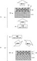
- (A), (b) It is a schematic diagram which shows the transmissive
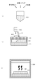
- (A)-(c) is explanatory drawing which shows the preparation process of the wavelength conversion member of this invention, respectively. It is explanatory drawing which shows the transmissive
- (A) to (c) are SEM photographs showing partial cross sections of the wavelength conversion member.
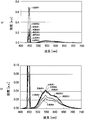
- (A), (b) is the graph which shows the emitted light intensity with respect to the wavelength in case laser power density of 40 W / mm ⁇ 2 >, respectively, and the enlarged graph. It is a graph which shows the emitted light intensity of the fluorescence with respect to a laser power density.
- FIG. 1A is a schematic diagram showing a transmissive light emitting device.
- the light emitting device 10 includes a light source 50 and a wavelength conversion member 100, and irradiates the light source light transmitted through the wavelength conversion member 100 and the light generated by excitation by the light source light in the wavelength conversion member 100. It emits light.
- the irradiation light can be, for example, white light.
- the light source 50 may be an LED (Light Emitting Diode) or LD (Laser Diode) chip.
- the LED generates light source light (excitation light) having a wavelength in a specific range according to the design of the light emitting device 10. For example, the LED generates blue light.
- an LD when used, coherent light with little variation in wavelength and phase can be generated.
- the light source 50 is not limited to these, and may generate light other than visible light, but preferably generates ultraviolet light, violet light, blue light, or green light.
- Such a light emitting device 10 can be expected to be highly effective when applied to lighting of public facilities that illuminates a wide area from high places such as factories, stadiums, and museums, or lighting that illuminates long distances such as automobile headlamps.
- the wavelength conversion member 100 includes a substrate 110 and a phosphor layer 120, is formed in a plate shape, and generates light having different wavelengths by being excited by the light source light while transmitting the light source light. For example, green, red, and yellow fluorescence converted by the phosphor layer can be transmitted and radiated while transmitting blue light source light.
- the base material 110 is formed in a plate shape and can be made of, for example, an inorganic material such as glass or sapphire that transmits light from the light source.
- the substrate 110 is preferably made of sapphire having high thermal conductivity.
- the phosphor layer 120 is provided as a film on the substrate 110, and is formed of phosphor particles 122 and translucent ceramics 121.
- the translucent ceramic 121 bonds the phosphor particles 122 to each other and bonds the substrate 110 and the phosphor particles 122 to each other.
- the portion where heat on the irradiation side is likely to generate heat is bonded to the base material 110 functioning as a heat radiating material with respect to the irradiation of light having a high energy density, so that heat can be radiated efficiently, and temperature quenching of the phosphor can be performed. Can be suppressed.
- the thickness of the phosphor layer 120 may be 2 to 400 ⁇ m, and preferably 30 to 80 ⁇ m.
- the translucent ceramic component fills the gaps between the phosphor particles at and near the interface with the substrate 110. Thereby, the heat dissipation path to the base material 110 is ensured, and the heat dissipation function is enhanced.
- the translucent ceramic 121 is an inorganic binder for holding the phosphor particles 122 and is made of, for example, silica (SiO 2) or aluminum phosphate.
- silica SiO 2
- aluminum phosphate aluminum phosphate
- YAG phosphor yttrium / aluminum / garnet phosphor
- LAG phosphor lutetium / aluminum / garnet phosphor
- the phosphor particles 122 can be selected from the following materials according to the design of the color to emit light.
- blue phosphors such as BaMgAl 10 O 17 : Eu, ZnS: Ag, Cl, BaAl 2 S 4 : Eu or CaMgSi 2 O 6 : Eu, Zn 2 SiO 4 : Mn, (Y, Gd) BO 3 : Tb, ZnS: Cu, Al, (M1) 2 SiO 4 : Eu, (M1) (M2) 2 S: Eu, (M3) 3 Al 5 O 12 : Ce, SiAlON: Eu, CaSiAlON: Eu, (M1) Yellow or green phosphor such as Si 2 O 2 N: Eu or (Ba, Sr, Mg) 2 SiO 4 : Eu, Mn, yellow such as (M1) 3 SiO 5 : Eu or (M1) S: Eu, orange or red phosphor, (Y, Gd) BO 3 : Eu, Y 2 O 2 S: Eu, (M1) 2
- M1 includes at least one of the group consisting of Ba, Ca, Sr, and Mg
- M2 includes at least one of Ga and Al
- M3 includes Y, Gd
- At least one of the group consisting of Lu and Te is included.
- said fluorescent substance particle 122 is an example, and the fluorescent substance particle 122 used for the wavelength conversion member 100 is not necessarily restricted above.
- the phosphor particles 122 include two types of particles having a predetermined particle size distribution. That is, two types of phosphor particles having different particle size distributions are included.
- the distribution of the predetermined particle diameter is a distribution having one peak such as a normal distribution and a Gaussian distribution.
- the two types of particles include large particles having a large average particle size and small particles having a small average particle size, and these two particle sizes occupy 70% by volume or more of the total.
- the ratio of the average particle diameter of the large particles to the average particle diameter of the small particles is 2 to 4, and the ratio of the volume of the large particles to the volume of the small particles is 5.7 or less.
- the small particles are mixed so that the ratio of the small particles is 8.5: 1.5 or more with respect to the large particles, thereby reducing the voids without reducing the light conversion efficiency by the large particles, Transmission of light from the light source can be suppressed. Moreover, even if light source light having a high laser power density is incident, rapid quenching due to heat storage can be suppressed.
- the average particle size of the large particles is preferably 10 to 20 ⁇ m, and the average particle size of the small particles is preferably 2.5 to 10 ⁇ m.
- the wavelength conversion member 100 suitable for the light emitting device 10 can be configured.
- the average particle size can be calculated by measuring the particle size of all particles from the SEM image of the polished cross section and creating frequency data of the particle size distribution. Even when the particle size is divided into two particle sizes, the particle size at two peaks can be obtained as the average particle size. Even when the peaks overlap, the approximate average particle size can be calculated from the shoulder of the peak.
- the ratio of the volume of large particles to the volume of small particles is preferably 5.7 or less. That is, the small particles are mixed with the large particles so that the volume ratio is 8.5: 1.5 or more, whereby the voids can be reduced and the transmission of the light source light can be more efficiently suppressed.
- the ratio of the volume of large particles to the volume of small particles is preferably 1.5 or more. That is, by mixing the large particles with the large particles so that the volume ratio is 6: 4 or less, the interface between the particles can be reduced, the thermal resistance can be reduced, and quenching can be suppressed.
- the frequency of the mode (which may be the average or median) Determine the ratio.
- the volume ratio can be calculated by calculating the volume of one particle, using the average particle diameter as the diameter of each particle, and multiplying the volume by the respective frequency ratio.
- phosphor particles having two particle size distributions are mixed at a certain ratio, and small particles are allowed to enter the gaps between the large particles, thereby suppressing the transmission of light from the light source and the phosphors.
- the void portion of the layer can be reduced and a heat dissipation path can be secured.
- FIG. 1B is a schematic diagram showing a reflective light emitting device 20.
- the light emitting device 20 includes a light source 50 and a wavelength conversion member 200, for example, light source light reflected by the wavelength conversion member 200 and light obtained by converting the wavelength of the light source light within the wavelength conversion member 100. And irradiating light such as white light can be emitted.
- the wavelength conversion member 200 includes a base material 210 and a phosphor layer 120 and is formed in a plate shape.
- the light source light is reflected by the base material 210 and excited by the light source light to generate light having different wavelengths.
- the substrate 210 is formed in a plate shape, and can be made of, for example, an inorganic material that reflects light from the light source.
- the substrate 210 is preferably made of aluminum.
- an Ag film is preferably formed on the surface of the substrate.
- the thickness of the phosphor layer 120 may be 2 to 400 ⁇ m, and preferably 20 to 80 ⁇ m.
- [Production method of wavelength conversion member] 2 (a) to 2 (c) are explanatory views showing the steps for producing the wavelength conversion member of the present invention.
- phosphor particles, an inorganic binder, and a dispersion medium are prepared.
- particles such as YAG and LAG can be used as the phosphor particles.
- the type and amount of the phosphor particles are adjusted according to the irradiation light to be obtained for the light source light. For example, when white light is to be obtained with respect to blue light, an appropriate amount of phosphor particles that emit green light, red light, or yellow light by excitation with blue light is selected.
- the inorganic binder for example, ethyl silicate obtained by dissolving a silicon precursor in ethanol can be used.
- the inorganic binder is obtained by reacting a raw material containing at least one member selected from the group consisting of a silicon oxide precursor that becomes silicon oxide by hydrolysis or oxidation, a silicate compound, silica, and amorphous silica at room temperature, or Or obtained by heat treatment at a temperature of 500 ° C. or lower.
- the silicon oxide precursor include those mainly composed of perhydropolysilazane, ethyl silicate, and methyl silicate.
- high boiling point solvents such as butanol, isophorone, terpineol, and glycerol, can be used.
- a paste (ink) 410 is prepared by mixing these inorganic binder, dispersion medium, and two kinds of large and small phosphor particles.
- a ball mill or the like can be used for mixing.
- a base material of an inorganic material is prepared. Glass or sapphire can be used for the substrate.
- the substrate is preferably plate-shaped.
- the obtained paste 410 is applied to the substrate 110 so as to have the above-mentioned film thickness with respect to the average particle diameter by screen printing.
- Screen printing can be performed by pressing the paste 410 with the ink squeegee 510 against the silk screen 520 stretched around the frame.
- the screen printing method there are a spray method, a drawing method using a dispenser, and an ink jet method, but the screen printing method is preferable in order to stably form a thin phosphor layer.
- the printed paste 410 is dried and heat-treated in a furnace 600 to fly away the dispersion medium and the organic content of the inorganic binder to remove the main metal in the inorganic binder. Oxidation (when the main metal is Si, SiO 2 is made), and at that time, the phosphor layer 120 and the substrate 110 are bonded.
- the wavelength conversion member 100 which can suppress transmission of light source light can be manufactured.
- the obtained wavelength conversion member can be suitably arranged and produced with respect to light sources, such as LED.
- Example 1 Evaluation of suppression of transmission of light source light
- Example 2 Sample Preparation Method Wavelength conversion members of Examples 1 to 4 and Comparative Examples 1 to 4 were prepared.
- two types of pastes were prepared by mixing ethyl silicate and terpineol as an inorganic binder and a dispersion medium for phosphor particles (YAG, hereinafter the same) of two types of particle sizes (average particle size 6 ⁇ m, 18 ⁇ m), respectively.
- Two types of pastes were mixed so that the two types of particles were constituted by the mixing ratio (volume ratio) shown in the table below.
- the prepared paste was applied to a sapphire plate serving as a substrate so as to have a thickness of 40 ⁇ m using a screen printing method, and heat-treated to obtain a sample of a wavelength conversion member.
- the average particle diameter of the phosphor particles in the wavelength conversion member is the average of the phosphor particles in the raw material. The value is equivalent to the particle diameter.
- the average particle size of the phosphor was measured using a laser diffraction / scattering particle size distribution measuring apparatus “HORIBA (Horiba, Ltd.) LA-960”.
- the volume ratio was calculated by dividing the density from the weight of the phosphor of each particle size.
- the emission intensity of the light source light was evaluated for Comparative Examples 1 to 4 and Examples 1 to 4 obtained as described above. Specifically, the sample was irradiated with a laser, and the emission intensity of the transmitted light from the laser input value was examined.
- the fluorescence emission intensity is a relative intensity obtained by making the numbers shown on the luminance meter dimensionless when the above evaluation system is used.
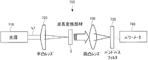
- FIG. 3 is an explanatory view showing a transmission type evaluation system for the wavelength conversion member.
- the transmissive evaluation system 700 includes a light source 710, a plano-convex lens 720, a biconvex lens 730, a band pass filter 735, and a power meter 740. Each element is arranged so that the transmitted light from the wavelength conversion member S can be collected and measured.
- the band-pass filter 735 is a filter that cuts light with a wavelength of 480 nm as a threshold, and a filter that cuts the larger wavelength side is used when measuring the transmitted light source light. In addition, when measuring the fluorescence emission intensity, a filter that cuts the side with the smaller wavelength is used. Thus, in order to separate the transmitted light source light (excitation light) from fluorescence, it is installed between the biconvex lens and the power meter.
- the light source light that has entered the plano-convex lens 720 is condensed on the focal point on the sample S of the wavelength conversion member. Then, the radiated light generated from the sample S is collected by the biconvex lens 730, and the intensity of the light obtained by cutting the collected light by the band pass filter 735 is measured by the power meter 740. This measured value is defined as fluorescence emission intensity.
- the energy density per unit area can be increased even with a low-power laser. This energy density is defined as the laser power density.
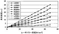
- FIG. 4 is a graph showing the emission intensity of the transmitted light source with respect to the laser power density. As shown in FIG. 4, when Comparative Example 1 and Comparative Example 4 were compared, it was confirmed that the sample of only large particles had higher intensity of the light source light that was transmitted than the small particles.
- Wavelength conversion members containing small particles have phosphor particles densely arranged on the base material, making it difficult for light source light to pass through them.
- wavelength conversion members with only large particles have many voids between the phosphor particles. Therefore, it is considered that the light source light is transmitted.
- FIGS. 6A and 6B are a graph showing an emission spectrum when the laser power density is 40 W / mm 2 and an enlarged graph thereof, respectively. As shown in FIGS. 6A and 6B, in Comparative Example 1, the intensity increased in the wavelength range corresponding to the blue light, and in Examples 1 to 4, the fluorescence intensity of Comparative Example 1 was maintained. It was confirmed that the transmission of the light source light was suppressed in the wavelength range corresponding to the blue light.
- FIG. 7 is a graph showing the emission intensity of fluorescence with respect to the laser power density.
- Comparative Example 1 and Comparative Example 4 confirmed that the measured fluorescence emission intensity was higher in the sample of Comparative Example 1 having only large particles than in the sample of Comparative Example 4 having only small particles. It is considered that the phosphor particles having a large particle diameter have higher conversion efficiency to fluorescence than the phosphor particles having a small particle diameter. On the other hand, in Examples 1 to 3, even if 1.5 to 30% (15% to 30%) of small particles are mixed with large particles, the conversion efficiency of the large particles is dominant and the emission intensity is reduced. It was confirmed that there was no.
- Small particles are densely arranged on the base material due to the small size of the particles, so there are few voids between the phosphor particles, and it is easy to secure a path to dissipate the heat generated in the phosphor layer. Fluorescence quenching due to heat storage is considered to be moderate.
Landscapes
- Chemical & Material Sciences (AREA)
- Physics & Mathematics (AREA)
- Engineering & Computer Science (AREA)
- Optics & Photonics (AREA)
- Materials Engineering (AREA)
- Organic Chemistry (AREA)
- General Physics & Mathematics (AREA)
- Inorganic Chemistry (AREA)
- Electromagnetism (AREA)
- Condensed Matter Physics & Semiconductors (AREA)
- General Engineering & Computer Science (AREA)
- Spectroscopy & Molecular Physics (AREA)
- Microelectronics & Electronic Packaging (AREA)
- Luminescent Compositions (AREA)
- Led Device Packages (AREA)
- Optical Filters (AREA)
- Semiconductor Lasers (AREA)
Abstract
Priority Applications (6)
| Application Number | Priority Date | Filing Date | Title |
|---|---|---|---|
| EP17789473.0A EP3451031B1 (fr) | 2016-04-25 | 2017-04-24 | Élément de conversion de longueur d'onde, son procédé de fabrication, et dispositif électroluminescent |
| KR1020187026382A KR102070569B1 (ko) | 2016-04-25 | 2017-04-24 | 파장 변환 부재, 그 제조 방법 및 발광 장치 |
| CN202310285301.2A CN116293491A (zh) | 2016-04-25 | 2017-04-24 | 波长转换构件、其制造方法及发光装置 |
| JP2017560823A JP6650951B2 (ja) | 2016-04-25 | 2017-04-24 | 波長変換部材、その製造方法および発光装置 |
| US16/092,687 US10590341B2 (en) | 2016-04-25 | 2017-04-24 | Wavelength conversion member, production method therefor, and light emitting device |
| CN201780022876.8A CN109073801A (zh) | 2016-04-25 | 2017-04-24 | 波长转换构件、其制造方法及发光装置 |
Applications Claiming Priority (2)
| Application Number | Priority Date | Filing Date | Title |
|---|---|---|---|
| JP2016087114 | 2016-04-25 | ||
| JP2016-087114 | 2016-04-25 |
Publications (1)
| Publication Number | Publication Date |
|---|---|
| WO2017188191A1 true WO2017188191A1 (fr) | 2017-11-02 |
Family
ID=60160437
Family Applications (1)
| Application Number | Title | Priority Date | Filing Date |
|---|---|---|---|
| PCT/JP2017/016240 Ceased WO2017188191A1 (fr) | 2016-04-25 | 2017-04-24 | Élément de conversion de longueur d'onde, son procédé de fabrication, et dispositif électroluminescent |
Country Status (7)
| Country | Link |
|---|---|
| US (1) | US10590341B2 (fr) |
| EP (1) | EP3451031B1 (fr) |
| JP (1) | JP6650951B2 (fr) |
| KR (1) | KR102070569B1 (fr) |
| CN (2) | CN109073801A (fr) |
| TW (1) | TWI657602B (fr) |
| WO (1) | WO2017188191A1 (fr) |
Cited By (3)
| Publication number | Priority date | Publication date | Assignee | Title |
|---|---|---|---|---|
| CN109782516A (zh) * | 2017-11-15 | 2019-05-21 | 中强光电股份有限公司 | 投影机及波长转换元件 |
| JP2022002266A (ja) * | 2020-06-22 | 2022-01-06 | ウシオ電機株式会社 | 半導体発光装置 |
| JPWO2022030400A1 (fr) * | 2020-08-07 | 2022-02-10 |
Families Citing this family (4)
| Publication number | Priority date | Publication date | Assignee | Title |
|---|---|---|---|---|
| US20220136679A1 (en) * | 2019-02-06 | 2022-05-05 | Sharp Kabushiki Kaisha | Wavelength conversion element, light source device, vehicle headlight, transmissive lighting device, display device, and lighting device |
| JP7429346B2 (ja) * | 2019-10-03 | 2024-02-08 | 国立研究開発法人物質・材料研究機構 | 波長変換部材 |
| CN113917776B (zh) * | 2020-07-09 | 2023-03-24 | 中强光电股份有限公司 | 波长转换装置以及投影装置 |
| CN120869902A (zh) * | 2025-09-28 | 2025-10-31 | 澳谱特科技(上海)有限公司 | 一种双光路动态图像粒度粒形分析仪 |
Citations (6)
| Publication number | Priority date | Publication date | Assignee | Title |
|---|---|---|---|---|
| JPH04332457A (ja) * | 1991-01-17 | 1992-11-19 | Toshiba Lighting & Technol Corp | 蛍光ランプおよびこれに用いる結着剤 |
| JP2009280793A (ja) * | 2008-04-24 | 2009-12-03 | Kyocera Corp | 蛍光体および波長変換器ならびに発光装置、照明装置 |
| JP2011238811A (ja) * | 2010-05-12 | 2011-11-24 | Konica Minolta Opto Inc | 波長変換素子および発光装置 |
| JP2015119172A (ja) * | 2013-11-13 | 2015-06-25 | 株式会社日本セラテック | 発光素子、発光装置、及びそれらの製造方法 |
| JP2015149394A (ja) * | 2014-02-06 | 2015-08-20 | スタンレー電気株式会社 | 波長変換体及びそれを用いた発光装置 |
| JP2016204561A (ja) * | 2015-04-24 | 2016-12-08 | 太平洋セメント株式会社 | 蛍光部材、その製造方法および発光装置 |
Family Cites Families (39)
| Publication number | Priority date | Publication date | Assignee | Title |
|---|---|---|---|---|
| JP3617587B2 (ja) * | 1997-07-17 | 2005-02-09 | 日亜化学工業株式会社 | 発光ダイオード及びその形成方法 |
| MY131962A (en) | 2001-01-24 | 2007-09-28 | Nichia Corp | Light emitting diode, optical semiconductor device, epoxy resin composition suited for optical semiconductor device, and method for manufacturing the same |
| WO2003021691A1 (fr) * | 2001-09-03 | 2003-03-13 | Matsushita Electric Industrial Co., Ltd. | Dispositif emetteur de lumiere a semi-conducteur, appareil emetteur de lumiere et procede de production d'un dispositif emetteur de lumiere a semi-conducteur |
| JP4207537B2 (ja) * | 2002-11-08 | 2009-01-14 | 日亜化学工業株式会社 | 蛍光体および発光装置 |
| KR101142725B1 (ko) * | 2003-03-13 | 2012-05-04 | 니치아 카가쿠 고교 가부시키가이샤 | 발광막, 발광장치, 발광막의 제조방법 및 발광장치의제조방법 |
| US7279832B2 (en) * | 2003-04-01 | 2007-10-09 | Innovalight, Inc. | Phosphor materials and illumination devices made therefrom |
| TW200531315A (en) * | 2004-01-26 | 2005-09-16 | Kyocera Corp | Wavelength converter, light-emitting device, method of producing wavelength converter and method of producing light-emitting device |
| CN101614340A (zh) * | 2005-09-01 | 2009-12-30 | 夏普株式会社 | 发光装置 |
| EP1995294A4 (fr) * | 2006-02-10 | 2012-06-06 | Mitsubishi Chem Corp | Phosphore, son procede de fabrication, composition contenant du phosphore, dispositif electroluminescent, affichage d'image, et dispositif d'eclairage |
| JP2009010315A (ja) | 2007-05-30 | 2009-01-15 | Sharp Corp | 蛍光体の製造方法、発光装置および画像表示装置 |
| JP2009019163A (ja) * | 2007-07-13 | 2009-01-29 | Sharp Corp | 発光装置用蛍光体粒子集合体、発光装置、および液晶表示用バックライト装置 |
| JP5371359B2 (ja) * | 2007-12-27 | 2013-12-18 | 豊田合成株式会社 | 蛍光体含有ガラス板及び発光装置の製造方法 |
| JP2009167338A (ja) * | 2008-01-18 | 2009-07-30 | Sharp Corp | 波長変換部材およびこれを備える発光装置、ならびに蛍光体 |
| WO2009154193A1 (fr) | 2008-06-16 | 2009-12-23 | 株式会社ニコン | Composition céramique, céramique de phosphore et son procédé de production, et dispositif électroluminescent |
| AU2010236468A1 (en) * | 2009-04-15 | 2011-10-13 | Research Triangle Institute | Stimulated lighting devices |
| JP5601833B2 (ja) | 2009-12-25 | 2014-10-08 | 日本ファインセラミックス株式会社 | 金属−セラミックス複合材料の製造方法 |
| JP4930649B1 (ja) * | 2011-02-25 | 2012-05-16 | 三菱化学株式会社 | ハロリン酸塩蛍光体、及び白色発光装置 |
| EP2555260A1 (fr) * | 2010-03-30 | 2013-02-06 | Mitsubishi Chemical Corporation | Dispositif électroluminescent |
| CN102939273A (zh) * | 2010-05-13 | 2013-02-20 | 电气化学工业株式会社 | β型赛隆的制造方法、β型赛隆及利用该β型赛隆的产品 |
| JP5864851B2 (ja) | 2010-12-09 | 2016-02-17 | シャープ株式会社 | 発光装置 |
| CN103403531A (zh) * | 2010-12-22 | 2013-11-20 | 皇家飞利浦电子股份有限公司 | 用于测试发光薄膜的方法和装置 |
| WO2012132232A1 (fr) * | 2011-03-31 | 2012-10-04 | パナソニック株式会社 | Dispositif luminescent à semi-conducteurs |
| JP5866870B2 (ja) * | 2011-08-26 | 2016-02-24 | 三菱化学株式会社 | 発光装置 |
| JP2013055269A (ja) * | 2011-09-06 | 2013-03-21 | Nippon Electric Glass Co Ltd | 波長変換部材および発光デバイス |
| US9309461B2 (en) * | 2011-09-26 | 2016-04-12 | Konica Minolta, Inc. | Phosphor dispersion liquid and method for manufacturing LED device |
| JP5744941B2 (ja) * | 2012-03-12 | 2015-07-08 | 富士フイルム株式会社 | 放射線画像検出装置及び放射線画像撮影システム |
| JPWO2013154133A1 (ja) * | 2012-04-13 | 2015-12-17 | シャープ株式会社 | 光散乱体、光散乱体膜、光散乱体基板、光散乱体デバイス、発光デバイス、表示装置、および照明装置 |
| EP2853577A4 (fr) * | 2012-08-13 | 2016-01-06 | Konica Minolta Inc | Procédé de fabrication de liquide de dispersion de luminophore et procédé de fabrication de dispositif de diode électroluminescente |
| WO2014103671A1 (fr) * | 2012-12-28 | 2014-07-03 | シャープ株式会社 | Dispositif électroluminescent |
| JP2015038960A (ja) | 2013-05-16 | 2015-02-26 | 株式会社日本セラテック | 発光装置 |
| EP3168531B1 (fr) * | 2013-06-21 | 2019-03-20 | Panasonic Intellectual Property Management Co., Ltd. | Élément de conversion de longueur d'onde, source de lumière et phare de véhicule |
| JP2015065425A (ja) | 2013-08-29 | 2015-04-09 | 株式会社日本セラテック | 発光装置及びその製造方法 |
| JP2015090887A (ja) | 2013-11-05 | 2015-05-11 | 株式会社日本セラテック | 発光素子及び発光装置 |
| WO2015041204A1 (fr) * | 2013-09-20 | 2015-03-26 | 旭硝子株式会社 | Élément de conversion de lumière, procédé de production d'élément de conversion de lumière, procédé de réglage de la chromaticité d'un élément de conversion de lumière, source de lumière d'éclairage, dispositif d'affichage à cristaux liquides |
| DE102014101804A1 (de) * | 2013-12-18 | 2015-06-18 | Osram Opto Semiconductors Gmbh | Optoelektronisches Bauelement und Verfahren zur Herstellung eines optoelektronischen Bauelements |
| JP6152801B2 (ja) | 2014-01-21 | 2017-06-28 | 豊田合成株式会社 | 発光装置及びその製造方法 |
| MY177277A (en) * | 2014-03-03 | 2020-09-10 | Covalent Mat Corporation | Wavelength converting member |
| JP6344157B2 (ja) | 2014-09-01 | 2018-06-20 | 日本電気硝子株式会社 | 波長変換部材の製造方法及び波長変換部材 |
| JP2017107071A (ja) * | 2015-12-10 | 2017-06-15 | 日本電気硝子株式会社 | 波長変換部材及び波長変換素子、並びにそれらを用いた発光装置 |
-
2017
- 2017-04-24 CN CN201780022876.8A patent/CN109073801A/zh active Pending
- 2017-04-24 KR KR1020187026382A patent/KR102070569B1/ko active Active
- 2017-04-24 CN CN202310285301.2A patent/CN116293491A/zh active Pending
- 2017-04-24 WO PCT/JP2017/016240 patent/WO2017188191A1/fr not_active Ceased
- 2017-04-24 EP EP17789473.0A patent/EP3451031B1/fr active Active
- 2017-04-24 JP JP2017560823A patent/JP6650951B2/ja active Active
- 2017-04-24 TW TW106113564A patent/TWI657602B/zh active
- 2017-04-24 US US16/092,687 patent/US10590341B2/en active Active
Patent Citations (6)
| Publication number | Priority date | Publication date | Assignee | Title |
|---|---|---|---|---|
| JPH04332457A (ja) * | 1991-01-17 | 1992-11-19 | Toshiba Lighting & Technol Corp | 蛍光ランプおよびこれに用いる結着剤 |
| JP2009280793A (ja) * | 2008-04-24 | 2009-12-03 | Kyocera Corp | 蛍光体および波長変換器ならびに発光装置、照明装置 |
| JP2011238811A (ja) * | 2010-05-12 | 2011-11-24 | Konica Minolta Opto Inc | 波長変換素子および発光装置 |
| JP2015119172A (ja) * | 2013-11-13 | 2015-06-25 | 株式会社日本セラテック | 発光素子、発光装置、及びそれらの製造方法 |
| JP2015149394A (ja) * | 2014-02-06 | 2015-08-20 | スタンレー電気株式会社 | 波長変換体及びそれを用いた発光装置 |
| JP2016204561A (ja) * | 2015-04-24 | 2016-12-08 | 太平洋セメント株式会社 | 蛍光部材、その製造方法および発光装置 |
Cited By (5)
| Publication number | Priority date | Publication date | Assignee | Title |
|---|---|---|---|---|
| CN109782516A (zh) * | 2017-11-15 | 2019-05-21 | 中强光电股份有限公司 | 投影机及波长转换元件 |
| JP2022002266A (ja) * | 2020-06-22 | 2022-01-06 | ウシオ電機株式会社 | 半導体発光装置 |
| JP7447694B2 (ja) | 2020-06-22 | 2024-03-12 | ウシオ電機株式会社 | 半導体発光装置 |
| JPWO2022030400A1 (fr) * | 2020-08-07 | 2022-02-10 | ||
| JP7834645B2 (ja) | 2020-08-07 | 2026-03-24 | デンカ株式会社 | 蛍光体塗料、塗膜、蛍光体基板および照明装置 |
Also Published As
| Publication number | Publication date |
|---|---|
| TWI657602B (zh) | 2019-04-21 |
| CN116293491A (zh) | 2023-06-23 |
| EP3451031B1 (fr) | 2022-03-09 |
| KR20180113573A (ko) | 2018-10-16 |
| EP3451031A4 (fr) | 2019-12-11 |
| JPWO2017188191A1 (ja) | 2018-05-10 |
| JP6650951B2 (ja) | 2020-02-19 |
| TW201742270A (zh) | 2017-12-01 |
| US10590341B2 (en) | 2020-03-17 |
| KR102070569B1 (ko) | 2020-01-29 |
| CN109073801A (zh) | 2018-12-21 |
| EP3451031A1 (fr) | 2019-03-06 |
| US20190127636A1 (en) | 2019-05-02 |
Similar Documents
| Publication | Publication Date | Title |
|---|---|---|
| CN108885286B (zh) | 波长转换构件、其制造方法及发光装置 | |
| TWI657602B (zh) | 波長轉換構件及其製造方法、以及發光裝置 | |
| TWI677115B (zh) | 波長轉換構件及發光裝置 | |
| TWI669375B (zh) | 波長轉換構件及發光裝置 | |
| CN110291430B (zh) | 波长转换构件 | |
| JP6990065B2 (ja) | 波長変換部材、その製造方法および発光装置 | |
| JP2021103247A (ja) | 波長変換部材および発光装置 |
Legal Events
| Date | Code | Title | Description |
|---|---|---|---|
| ENP | Entry into the national phase |
Ref document number: 2017560823 Country of ref document: JP Kind code of ref document: A |
|
| WWE | Wipo information: entry into national phase |
Ref document number: 1020187026382 Country of ref document: KR |
|
| NENP | Non-entry into the national phase |
Ref country code: DE |
|
| WWE | Wipo information: entry into national phase |
Ref document number: 2017789473 Country of ref document: EP |
|
| 121 | Ep: the epo has been informed by wipo that ep was designated in this application |
Ref document number: 17789473 Country of ref document: EP Kind code of ref document: A1 |
|
| ENP | Entry into the national phase |
Ref document number: 2017789473 Country of ref document: EP Effective date: 20181126 |