WO2017188364A1 - Amplificateur optique, dispositif de tomographie de cohérence optique comprenant l'amplificateur optique, et procédé d'amplification optique utilisant l'amplificateur optique - Google Patents
Amplificateur optique, dispositif de tomographie de cohérence optique comprenant l'amplificateur optique, et procédé d'amplification optique utilisant l'amplificateur optique Download PDFInfo
- Publication number
- WO2017188364A1 WO2017188364A1 PCT/JP2017/016689 JP2017016689W WO2017188364A1 WO 2017188364 A1 WO2017188364 A1 WO 2017188364A1 JP 2017016689 W JP2017016689 W JP 2017016689W WO 2017188364 A1 WO2017188364 A1 WO 2017188364A1
- Authority
- WO
- WIPO (PCT)
- Prior art keywords
- light
- wavelength
- optical amplifier
- optical
- gain
- Prior art date
- Legal status (The legal status is an assumption and is not a legal conclusion. Google has not performed a legal analysis and makes no representation as to the accuracy of the status listed.)
- Ceased
Links
Images









Classifications
-
- A—HUMAN NECESSITIES
- A61—MEDICAL OR VETERINARY SCIENCE; HYGIENE
- A61B—DIAGNOSIS; SURGERY; IDENTIFICATION
- A61B3/00—Apparatus for testing the eyes; Instruments for examining the eyes
- A61B3/10—Objective types, i.e. instruments for examining the eyes independent of the patients' perceptions or reactions
- A61B3/102—Objective types, i.e. instruments for examining the eyes independent of the patients' perceptions or reactions for optical coherence tomography [OCT]
-
- A—HUMAN NECESSITIES
- A61—MEDICAL OR VETERINARY SCIENCE; HYGIENE
- A61B—DIAGNOSIS; SURGERY; IDENTIFICATION
- A61B3/00—Apparatus for testing the eyes; Instruments for examining the eyes
- A61B3/10—Objective types, i.e. instruments for examining the eyes independent of the patients' perceptions or reactions
-
- A—HUMAN NECESSITIES
- A61—MEDICAL OR VETERINARY SCIENCE; HYGIENE
- A61B—DIAGNOSIS; SURGERY; IDENTIFICATION
- A61B3/00—Apparatus for testing the eyes; Instruments for examining the eyes
- A61B3/10—Objective types, i.e. instruments for examining the eyes independent of the patients' perceptions or reactions
- A61B3/12—Objective types, i.e. instruments for examining the eyes independent of the patients' perceptions or reactions for looking at the eye fundus, e.g. ophthalmoscopes
- A61B3/1225—Objective types, i.e. instruments for examining the eyes independent of the patients' perceptions or reactions for looking at the eye fundus, e.g. ophthalmoscopes using coherent radiation
-
- G—PHYSICS
- G01—MEASURING; TESTING
- G01B—MEASURING LENGTH, THICKNESS OR SIMILAR LINEAR DIMENSIONS; MEASURING ANGLES; MEASURING AREAS; MEASURING IRREGULARITIES OF SURFACES OR CONTOURS
- G01B9/00—Measuring instruments characterised by the use of optical techniques
- G01B9/02—Interferometers
- G01B9/02001—Interferometers characterised by controlling or generating intrinsic radiation properties
-
- G—PHYSICS
- G01—MEASURING; TESTING
- G01B—MEASURING LENGTH, THICKNESS OR SIMILAR LINEAR DIMENSIONS; MEASURING ANGLES; MEASURING AREAS; MEASURING IRREGULARITIES OF SURFACES OR CONTOURS
- G01B9/00—Measuring instruments characterised by the use of optical techniques
- G01B9/02—Interferometers
- G01B9/0209—Low-coherence interferometers
- G01B9/02091—Tomographic interferometers, e.g. based on optical coherence
-
- G—PHYSICS
- G01—MEASURING; TESTING
- G01N—INVESTIGATING OR ANALYSING MATERIALS BY DETERMINING THEIR CHEMICAL OR PHYSICAL PROPERTIES
- G01N21/00—Investigating or analysing materials by the use of optical means, i.e. using sub-millimetre waves, infrared, visible or ultraviolet light
- G01N21/01—Arrangements or apparatus for facilitating the optical investigation
-
- G—PHYSICS
- G01—MEASURING; TESTING
- G01N—INVESTIGATING OR ANALYSING MATERIALS BY DETERMINING THEIR CHEMICAL OR PHYSICAL PROPERTIES
- G01N21/00—Investigating or analysing materials by the use of optical means, i.e. using sub-millimetre waves, infrared, visible or ultraviolet light
- G01N21/17—Systems in which incident light is modified in accordance with the properties of the material investigated
-
- H—ELECTRICITY
- H01—ELECTRIC ELEMENTS
- H01S—DEVICES USING THE PROCESS OF LIGHT AMPLIFICATION BY STIMULATED EMISSION OF RADIATION [LASER] TO AMPLIFY OR GENERATE LIGHT; DEVICES USING STIMULATED EMISSION OF ELECTROMAGNETIC RADIATION IN WAVE RANGES OTHER THAN OPTICAL
- H01S5/00—Semiconductor lasers
- H01S5/02—Structural details or components not essential to laser action
- H01S5/026—Monolithically integrated components, e.g. waveguides, monitoring photo-detectors, drivers
-
- H—ELECTRICITY
- H01—ELECTRIC ELEMENTS
- H01S—DEVICES USING THE PROCESS OF LIGHT AMPLIFICATION BY STIMULATED EMISSION OF RADIATION [LASER] TO AMPLIFY OR GENERATE LIGHT; DEVICES USING STIMULATED EMISSION OF ELECTROMAGNETIC RADIATION IN WAVE RANGES OTHER THAN OPTICAL
- H01S5/00—Semiconductor lasers
- H01S5/04—Processes or apparatus for excitation, e.g. pumping, e.g. by electron beams
- H01S5/042—Electrical excitation ; Circuits therefor
- H01S5/0425—Electrodes, e.g. characterised by the structure
- H01S5/04256—Electrodes, e.g. characterised by the structure characterised by the configuration
-
- H—ELECTRICITY
- H01—ELECTRIC ELEMENTS
- H01S—DEVICES USING THE PROCESS OF LIGHT AMPLIFICATION BY STIMULATED EMISSION OF RADIATION [LASER] TO AMPLIFY OR GENERATE LIGHT; DEVICES USING STIMULATED EMISSION OF ELECTROMAGNETIC RADIATION IN WAVE RANGES OTHER THAN OPTICAL
- H01S5/00—Semiconductor lasers
- H01S5/06—Arrangements for controlling the laser output parameters, e.g. by operating on the active medium
- H01S5/062—Arrangements for controlling the laser output parameters, e.g. by operating on the active medium by varying the potential of the electrodes
- H01S5/0625—Arrangements for controlling the laser output parameters, e.g. by operating on the active medium by varying the potential of the electrodes in multi-section lasers
-
- H—ELECTRICITY
- H01—ELECTRIC ELEMENTS
- H01S—DEVICES USING THE PROCESS OF LIGHT AMPLIFICATION BY STIMULATED EMISSION OF RADIATION [LASER] TO AMPLIFY OR GENERATE LIGHT; DEVICES USING STIMULATED EMISSION OF ELECTROMAGNETIC RADIATION IN WAVE RANGES OTHER THAN OPTICAL
- H01S5/00—Semiconductor lasers
- H01S5/06—Arrangements for controlling the laser output parameters, e.g. by operating on the active medium
- H01S5/068—Stabilisation of laser output parameters
-
- H—ELECTRICITY
- H01—ELECTRIC ELEMENTS
- H01S—DEVICES USING THE PROCESS OF LIGHT AMPLIFICATION BY STIMULATED EMISSION OF RADIATION [LASER] TO AMPLIFY OR GENERATE LIGHT; DEVICES USING STIMULATED EMISSION OF ELECTROMAGNETIC RADIATION IN WAVE RANGES OTHER THAN OPTICAL
- H01S5/00—Semiconductor lasers
- H01S5/20—Structure or shape of the semiconductor body to guide the optical wave ; Confining structures perpendicular to the optical axis, e.g. index or gain guiding, stripe geometry, broad area lasers, gain tailoring, transverse or lateral reflectors, special cladding structures, MQW barrier reflection layers
- H01S5/22—Structure or shape of the semiconductor body to guide the optical wave ; Confining structures perpendicular to the optical axis, e.g. index or gain guiding, stripe geometry, broad area lasers, gain tailoring, transverse or lateral reflectors, special cladding structures, MQW barrier reflection layers having a ridge or stripe structure
-
- H—ELECTRICITY
- H01—ELECTRIC ELEMENTS
- H01S—DEVICES USING THE PROCESS OF LIGHT AMPLIFICATION BY STIMULATED EMISSION OF RADIATION [LASER] TO AMPLIFY OR GENERATE LIGHT; DEVICES USING STIMULATED EMISSION OF ELECTROMAGNETIC RADIATION IN WAVE RANGES OTHER THAN OPTICAL
- H01S5/00—Semiconductor lasers
- H01S5/50—Amplifier structures not provided for in groups H01S5/02 - H01S5/30
-
- H—ELECTRICITY
- H01—ELECTRIC ELEMENTS
- H01S—DEVICES USING THE PROCESS OF LIGHT AMPLIFICATION BY STIMULATED EMISSION OF RADIATION [LASER] TO AMPLIFY OR GENERATE LIGHT; DEVICES USING STIMULATED EMISSION OF ELECTROMAGNETIC RADIATION IN WAVE RANGES OTHER THAN OPTICAL
- H01S5/00—Semiconductor lasers
- H01S5/50—Amplifier structures not provided for in groups H01S5/02 - H01S5/30
- H01S5/5027—Concatenated amplifiers, i.e. amplifiers in series or cascaded
-
- H—ELECTRICITY
- H01—ELECTRIC ELEMENTS
- H01S—DEVICES USING THE PROCESS OF LIGHT AMPLIFICATION BY STIMULATED EMISSION OF RADIATION [LASER] TO AMPLIFY OR GENERATE LIGHT; DEVICES USING STIMULATED EMISSION OF ELECTROMAGNETIC RADIATION IN WAVE RANGES OTHER THAN OPTICAL
- H01S5/00—Semiconductor lasers
- H01S5/04—Processes or apparatus for excitation, e.g. pumping, e.g. by electron beams
- H01S5/042—Electrical excitation ; Circuits therefor
- H01S5/0425—Electrodes, e.g. characterised by the structure
- H01S5/04254—Electrodes, e.g. characterised by the structure characterised by the shape
-
- H—ELECTRICITY
- H01—ELECTRIC ELEMENTS
- H01S—DEVICES USING THE PROCESS OF LIGHT AMPLIFICATION BY STIMULATED EMISSION OF RADIATION [LASER] TO AMPLIFY OR GENERATE LIGHT; DEVICES USING STIMULATED EMISSION OF ELECTROMAGNETIC RADIATION IN WAVE RANGES OTHER THAN OPTICAL
- H01S5/00—Semiconductor lasers
- H01S5/10—Construction or shape of the optical resonator, e.g. extended or external cavity, coupled cavities, bent-guide, varying width, thickness or composition of the active region
- H01S5/1082—Construction or shape of the optical resonator, e.g. extended or external cavity, coupled cavities, bent-guide, varying width, thickness or composition of the active region with a special facet structure, e.g. structured, non planar, oblique
- H01S5/1085—Oblique facets
-
- H—ELECTRICITY
- H01—ELECTRIC ELEMENTS
- H01S—DEVICES USING THE PROCESS OF LIGHT AMPLIFICATION BY STIMULATED EMISSION OF RADIATION [LASER] TO AMPLIFY OR GENERATE LIGHT; DEVICES USING STIMULATED EMISSION OF ELECTROMAGNETIC RADIATION IN WAVE RANGES OTHER THAN OPTICAL
- H01S5/00—Semiconductor lasers
- H01S5/10—Construction or shape of the optical resonator, e.g. extended or external cavity, coupled cavities, bent-guide, varying width, thickness or composition of the active region
- H01S5/18—Surface-emitting [SE] lasers, e.g. having both horizontal and vertical cavities
- H01S5/183—Surface-emitting [SE] lasers, e.g. having both horizontal and vertical cavities having only vertical cavities, e.g. vertical cavity surface-emitting lasers [VCSEL]
- H01S5/18361—Structure of the reflectors, e.g. hybrid mirrors
- H01S5/18363—Structure of the reflectors, e.g. hybrid mirrors comprising air layers
- H01S5/18366—Membrane DBR, i.e. a movable DBR on top of the VCSEL
-
- H—ELECTRICITY
- H01—ELECTRIC ELEMENTS
- H01S—DEVICES USING THE PROCESS OF LIGHT AMPLIFICATION BY STIMULATED EMISSION OF RADIATION [LASER] TO AMPLIFY OR GENERATE LIGHT; DEVICES USING STIMULATED EMISSION OF ELECTROMAGNETIC RADIATION IN WAVE RANGES OTHER THAN OPTICAL
- H01S5/00—Semiconductor lasers
- H01S5/30—Structure or shape of the active region; Materials used for the active region
- H01S5/34—Structure or shape of the active region; Materials used for the active region comprising quantum well or superlattice structures, e.g. single quantum well [SQW] lasers, multiple quantum well [MQW] lasers or graded index separate confinement heterostructure [GRINSCH] lasers
- H01S5/3408—Structure or shape of the active region; Materials used for the active region comprising quantum well or superlattice structures, e.g. single quantum well [SQW] lasers, multiple quantum well [MQW] lasers or graded index separate confinement heterostructure [GRINSCH] lasers characterised by specially shaped wells, e.g. triangular
Definitions
- the present invention relates to an optical amplifier that amplifies light emitted from a wavelength tunable light source, an optical coherence tomometer including the same, and an optical amplification method using the optical amplifier.
- OCT optical coherence tomography
- OCT optical coherence tomography
- SS-OCT Synwept Source OCT, hereinafter abbreviated as SS-OCT
- light emitted from a wavelength tunable light source is divided into irradiation light for irradiating an object and reference light, and the reference light and reflected light returning from different depths of the object are caused to interfere with each other.
- the frequency component included in the temporal waveform (interference signal) of the intensity of the interference light information relating to the tomography of the object, specifically a tomographic image can be obtained.
- OCT is used in industrial applications such as ophthalmology, cardiology, dermatology, and inspection of semiconductor chips.
- a wavelength tunable light source that changes the oscillation wavelength by displacing one of the two reflecting mirrors of a vertical cavity surface emitting laser (Vertical Cavity Surface Emitting Laser, VCSEL) is known. It has been.
- VCSEL Vertical Cavity Surface Emitting Laser
- MEMS-VCSEL a mechanism using MEMS
- the MEMS-VCSEL is known as being capable of changing the wavelength at high speed and increasing the coherence length, and is therefore suitable as a variable wavelength light source used for SS-OCT.
- Non-Patent Document 1 necessary light output intensity is obtained by inductively amplifying light emitted from the MEMS-VCSEL using an optical amplifier (BOA, Booster Optical Amplifier).
- Non-Patent Document 1 When amplified using BOA, ASE (Amplified Spontaneous Emission) light is generated from the BOA itself.
- the ASE light is spontaneous emission light generated from the BOA itself, and the ASE light includes light having a wavelength other than the wavelength to be amplified. Therefore, noise is included in the OCT signal obtained by irradiation with light including ASE light.
- Non-Patent Document 1 describes that the amplification factor of BOA with respect to incident light whose wavelength changes with time is changed with time. By increasing the amount of current injected into the BOA, the amplification factor can be increased and light having a required intensity at a certain wavelength can be obtained. However, only by adjusting the amount of current, even if a necessary light output intensity at a certain wavelength is obtained, the intensity of ASE light including light of an unnecessary wavelength may increase. Non-Patent Document 1 does not disclose any control for reducing the ASE light of the BOA.
- an object of the present invention is to provide an optical amplifier capable of reducing ASE light including light having an unnecessary wavelength while obtaining sufficient light output intensity at a necessary wavelength.
- the optical amplifier according to the present invention has a stacked body including two electrode layers and an active layer provided between them, and the stacked body guides light in the in-plane direction of the active layer.
- the region to be amplified can be changed in addition to the amplification factor of the optical amplifier. it can. Therefore, it is possible to reduce ASE light including light having an unnecessary wavelength while obtaining sufficient light output intensity at a necessary wavelength.
- FIG. 2A is a cross-sectional view of an electrode region (aa ′ cross section) and (b) a non-electrode region (bb ′ cross section) in the top view of the SOA according to the first embodiment of the present invention, and FIG. Sectional view of c ').
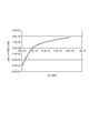
- the graph showing the gain spectrum of the active layer of SOA of Embodiment 1 of this invention The graph showing the relationship between the carrier density N in SOA of Embodiment 1 of this invention, and the sum total ⁇ g (N) of the positive gain obtained in the object wavelength range.
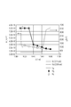
- 3 is a graph showing a relationship between an incident light wavelength ⁇ and L g , N g , and N a for achieving an optimum driving state in the SOA according to the first embodiment of the present invention.
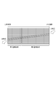
- 3 is a graph showing a relationship between an incident light wavelength ⁇ and a carrier density N in each electrode region for achieving an optimum driving state in the SOA according to the first embodiment of the present invention.
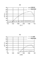
- the graph showing the relationship between the wavelength ⁇ and the incident light wavelength (a) 1030, (b) g (N, ⁇ ) ⁇ L in the optimum driving state in the SOA and the single electrode configuration SOA according to the first embodiment of the present invention. .
- FIG. 6 is a graph showing the relationship between the wavelength ⁇ and the incident light wavelength (a) 1030 and (b) g (N, ⁇ ) ⁇ L that is optimally driven at 1060 nm in the SOA and the single electrode configuration SOA according to the second embodiment of the present invention. .
- FIG. 6 is a graph showing the relationship between the wavelength ⁇ and the incident light wavelength (a) 1030 and (b) g (N, ⁇ ) ⁇ L that is optimally driven at 1060 nm in the SOA and the single electrode configuration SOA according to the second embodiment of the present invention. .
- the graph showing the sweep spectrum of the target emission light in SOA of Embodiment 4 of this invention.
- 10 is a graph showing a relationship between an incident light wavelength ⁇ and a carrier density N in each electrode region for achieving an optimum driving state in the SOA according to the fourth embodiment of the present invention.
- FIG. 6 is a graph showing the relationship between the wavelength ⁇ and the incident light wavelength (a) 1030 and (b) g (N, ⁇ ) ⁇ L that is optimally driven at 1060 nm in the SOA and the single electrode configuration SOA according to the second embodiment of the present invention. .
- optical amplifier according to the embodiment of the present invention will be described, the present invention is not limited to these.
- the optical amplifier according to the present embodiment has a stacked structure including two electrode layers and an active layer provided therebetween.
- the laminated body there is a structure having a lower electrode layer, a lower cladding layer, an active layer, an upper cladding layer, a contact layer, and an upper electrode layer in this order.
- What the stack is made of a semiconductor is called a semiconductor optical amplifier (hereinafter sometimes abbreviated as SOA).
- SOA semiconductor optical amplifier
- the end surface of the laminate on the side on which light is incident on the SOA may be referred to as the incident end surface
- the end surface on the side from which light is emitted may be referred to as the emission end surface
- This laminate has a waveguide through which light is guided in the in-plane direction of the active layer, and incident light on the end face side (incident end face side) in the in-plane direction of the laminate passes through the waveguide and is laminated. Amplified and emitted from the other end face side (injection end face side) in the in-plane direction of the body.
- the waveguide structure include a ridge waveguide in which an upper electrode layer, an upper contact layer, and an upper cladding layer form a ridge structure.
- At least one of the two electrode layers provided above and below the active layer has an electrode group composed of two or more electrodes provided separately in the waveguide direction of the waveguide.
- the optical amplifier according to the present embodiment uses two or more electrodes constituting an electrode group, and independently injects current into a plurality of different regions in the active layer, so that the optical amplifier according to the wavelength of incident light.
- the amplification factor can be changed.
- the optical amplifier according to this embodiment changes the amplification factor of incident light according to the wavelength of incident light, thereby selectively amplifying only the necessary wavelength to obtain sufficient light output intensity, Generation of ASE light including light of unnecessary wavelength can be suppressed as much as possible. For example, when it is desired to amplify light of wavelength ⁇ 1 out of incident light, the amount of current injected into the optical amplifier is adjusted, and light of wavelength ⁇ 1 is emitted from the optical amplifier with sufficient light output intensity. Like that. If the emitted light contains ASE light including unnecessary wavelengths, the region where light is amplified by injecting current into the optical amplifier is shortened to include light having a wavelength other than ⁇ 1. Reduce generation of ASE light.
- the optical amplifier in addition to the current injection amount (current density) into the optical amplifier, by changing the region where the light is amplified, it is possible to amplify a specific wavelength and suppress amplification of other wavelengths.
- the region where the light is amplified can be adjusted because the electrode layer constituting the laminate is provided by being separated into a plurality of electrodes, and current injection can be controlled independently. Control of the amount of current injected into each electrode is controlled by the control unit.
- the optical amplifier and the control unit may be collectively referred to as a light source system.
- the region in the waveguide, where the gain is positive at the wavelength of the incident light is defined as the gain region, and the total length of the gain regions along the waveguide is defined as the gain length.
- the gain region is defined as the gain region
- the total length of the gain regions along the waveguide is defined as the gain length.
- the current density of the current injected into the active layer is large, it is easy to amplify short wavelength light and it is difficult to amplify long wavelength light. Therefore, the shorter the wavelength of incident light, the more injected into the active layer. It is preferable to increase the current density.
- the waveform (spectral shape) of the wavelength change of the light emitted from the optical amplifier has either a substantially Gaussian shape or a substantially cosine tapered shape. This is because when such spectrally shaped light is used as OCT measurement light, it is easy to obtain an OCT image with less noise.
- the substantially Gaussian shape, the substantially rectangular shape, and the substantially cosine taper shape are not only Gaussian shape and cosine taper shape, but are slightly deviated from the Gaussian shape and cosine taper shape within a range in which large noise does not appear in the OCT image. It is a concept that includes a shape.
- the electrode group is composed of at least three electrodes and no current is injected into at least one electrode of the electrode group
- the electrode to which no current is injected is provided at a position closest to the incident end face of the laminate. It is preferably not an electrode.
- the electrode into which no current is injected is preferably an electrode provided at a position closest to the end face from which light is emitted.
- the current density of the electrode group is substantially the same.
- the gain in one optical width device can be changed with time mainly by the current density in the electrode region.
- a region where the gain at the center wavelength of incident light is positive is defined as a gain region, and a region where the gain is zero or less is defined as a non-gain region.
- optical amplifier according to the embodiment of the present invention will be described in detail with a specific configuration.
- the configurations, dimensions, materials, and control methods given in the following embodiments are merely examples, and the present invention is not limited to these.
- MEMS-VCSEL will be described as an example of a wavelength swept light source that performs wavelength sweeping by the MEMS mechanism.
- the MEMS-VCSEL of this example is configured to displace one mirror (sometimes referred to as a MEMS mirror) that constitutes a VCSEL resonator by electrostatic attraction.
- Embodiment 1 of the present invention will be described below.
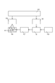
- the same signal is sent from a waveform generator 101 to a voltage amplifier 103 that controls the MEMS driving of the wavelength swept light source 102 and a current controller (control unit) 105 that controls the driving of the SOA 104.
- a current controller control unit
- the MEMS drive of the wavelength swept light source 102 and the drive of the SOA 104 can be synchronized in time. Therefore, by grasping the relationship between the voltage value for controlling the displacement of the MEMS mirror of the wavelength swept light source 102 and the oscillation wavelength in advance, the drive current value of the SOA 104 can be controlled according to the oscillation wavelength. become.
- an isolator 107 is provided between the wavelength swept light source 102 and the SOA 104 in order to suppress return light to the wavelength swept light source 102.
- FIG. 2 is a perspective view (b) of the SOA in this embodiment, and is a top view of the SOA.
- 3A is a cross-sectional view of a region (aa ′ cross section) where an SOA electrode is provided in the present embodiment
- FIG. 3B is a non-electrode region (bb ′ cross section) where no electrode is provided.
- FIG. 3C is a sectional view of the optical waveguide (c-c ′ section) of the SOA in the present embodiment.
- all electrodes are connected to a drive system (driver), and the amount of current (current density) injected into the active layer can be controlled independently for each electrode region. It has a mechanism.
- n-Al 0.9 GaAs as an n-type cladding layer 211 is sequentially epitaxially grown on the GaAs substrate 210 by using, for example, a MOCVD (Metal Organic Chemical Vapor Deposition) method.
- MOCVD Metal Organic Chemical Vapor Deposition
- GaIn 0.3 As having a single quantum well structure as the active layer 205, p-Al 0.9 GaAs as the p-type cladding layer 212, and highly doped p-GaAs as the contact layer 213 are epitaxially grown sequentially.
- a ridge 206 is formed on the wafer on which each layer is laminated by a general photolithography method and wet / dry etching to form an optical waveguide.
- the ridge 206 By forming the ridge 206, light can be confined and guided in the waveguide portion in the active layer.
- a stripe mask for forming an optical waveguide is formed of a photoresist using a photolithography method. Thereafter, SiO 2 is selectively removed by wet etching, and the semiconductor other than the mask is selectively removed by dry etching. At this time, the part to be removed is halfway between the contact layer 213 and the p-type cladding layer 212.
- the width of the optical waveguide is 3 ⁇ m in order to achieve a single mode.
- the optical waveguide In order to suppress reflection at the incident end face 201 and the exit end face 202, the optical waveguide is inclined about 7 degrees with respect to the normal direction of each end face in the vicinity of the end face.
- the p-electrode 203 is formed using a vacuum deposition method and photolithography.
- the p electrode 203 is, for example, Ti / Au, and a plurality of p electrodes 203 are arranged on the optical waveguide in a state where they are insulated in series with respect to the waveguide direction. Further, the contact layer 213 in the non-electrode region is removed by wet etching using citric acid perwater to form an electrically insulated region.
- the substrate 210 is thinned to a thickness of about 100 ⁇ m by polishing. By doing so, cleavage on the facet surface is facilitated. Then, the n electrode 204 is formed by a vacuum evaporation method.
- the n electrode 204 is, for example, AuGe / Ni / Au.
- annealing is performed in a high-temperature nitrogen atmosphere to alloy both electrodes and the semiconductor.
- a facet surface is formed on the incident end face 201 and the exit end face 202 by cleavage, thereby completing the SOA element.
- the substrate 210 may be a p-type GaAs substrate, in which case the conductivity type of each semiconductor layer is changed accordingly.
- the active layer 205 has an example of a single quantum well (SQW) structure
- a multiple quantum well (MQW) structure having a plurality of quantum wells may be used.
- the MQW structure may be an asymmetric multiple quantum well (A-MQW) structure (asymmetric quantum well structure) in which the composition and well width are the same, or at least one of the plurality of quantum wells has a different composition or well width. Good.
- the material constituting the quantum well is not limited to the above-described materials, and a light emitting material such as GaAs, GaInP, AlGaInN, AlGaInAsP, AlGaAsSb may be used.
- the active layer 205 has a single thickness and a single composition with respect to the waveguide direction, but is not limited to this as long as the effects of the present invention can be obtained.
- the optical waveguide has a linear shape, a constant width, and a shape capable of obtaining a constant refractive index, but is not limited to this as long as the effect of the present invention can be obtained.
- the optical waveguide shape may be bent or branched, and the width or refractive index of the optical waveguide may be changed in the waveguide direction.
- the optical waveguide width is 3 ⁇ m so that the light emitted from the SOA becomes a single (single) mode
- it may be made to be a multi (multi) mode.
- a stripe type active layer or a current blocking layer may be introduced to confine the current or light.
- the SOA in the present embodiment shows an example in which the optical waveguide is inclined by about 7 degrees with respect to the normal direction of each end face in the vicinity of the end face in order to suppress reflection at each end face of the entrance end face and the exit end face.
- the angle is not limited to 7 °.
- the number of electrodes included in the electrode group is three is shown, but the number of electrodes satisfying the requirement for obtaining the effect of the present invention (two or more) is not limited thereto.
- a non-gain region may be formed in the vicinity of the end face in order to suppress concentration of light and current on the end face of the incident end face 201 and / or the end face 202 of the emission.
- An antireflection (AR) film may be formed on the end face in order to suppress reflection at the end face of the incident end face 201 or the exit end face 202 or both.
- a configuration in which a plurality of n electrodes 204 or both electrodes are arranged may be used.
- the SOA driving state is defined by the carrier density, but in practice, the current density in each electrode region is adjusted so that the carrier density in the gain region and the non-gain region becomes a desired value.
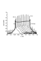
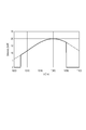
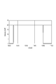
- the sweep spectrum of the MEMS-VCSEL having a center wavelength near 1060 nm as the incident light (FIG. 4) and the sweep spectrum shape (shown by a solid line in FIG. 5) represented by the following equation as the target emission light Assumed.
- FIG. 4 quotes Electron Let 2012 Oct 11 48 (21) 1331-1333.
- ⁇ is the wavelength and P is the light intensity.
- This sweep spectrum has a Gaussian shape (indicated by a dotted line in FIG. 5) having a center wavelength of 1060 nm, a light intensity at the center wavelength of 20 mW, and a full width at half maximum of 90 nm in the sweep wavelength range (1010 to 1080 nm) of incident light. In other wavelength ranges, the light intensity is 0 mW.
- the plurality of gain regions have the same carrier density. Further, the carrier density is such that the gain at the incident light wavelength is zero in the non-gain region.
- ⁇ wavelength (1010 to 1080 nm)
- P in ( ⁇ ) incident light intensity at wavelength ⁇
- P out ( ⁇ ) emitted light intensity at wavelength ⁇ .
- G (N, ⁇ ): SOA gain at wavelength ⁇ at carrier density N, L g : total length of SOA gain region, and ⁇ : confinement factor in SOA optical waveguide. In the following, calculation results with ⁇ 0.03 are shown.
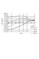
- FIG. 6 shows a gain spectrum in the active layer of the SOA of the present embodiment.
- ⁇ g (N) is used as an index representing the total amount of ASE light per unit length of the gain region generated from the SOA itself at the carrier density N in the target wavelength range.
- the optimum driving state refers to a driving state in which incident light of a certain wavelength (in this case, wavelength 1060 nm) is amplified and ASE light is reduced as much as possible so as to form a desired sweep spectrum.
- the driving state here refers to a combination of the length of each electrode region and the carrier density in those electrode regions. In other words, when the total length (gain length) and carrier density of the gain region are L g and N g , respectively, and the total length of the non-gain region (non-gain length) and the carrier density are L a and N a , respectively, optimum driving In order to determine the state, it is necessary to determine these four values.
- N g and N a for obtaining the optimum driving state are obtained.
- g (N, ⁇ ) / ⁇ g (N) represents the magnitude of the gain at the wavelength ⁇ with respect to the total amount of ASE light in the target wavelength range, and the larger the value, the smaller the wavelength ⁇ while suppressing the amount of ASE light. This means that incident light can be amplified efficiently.
- g (N, ⁇ ) / ⁇ g (N) represents the magnitude of the gain at the wavelength ⁇ with respect to the total amount of ASE light in the target wavelength range, and the larger the value, the smaller the wavelength ⁇ while suppressing the amount of ASE light. This
- N g for achieving the state is determined to be 2.2E + 18 / cm 3 .
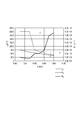
- FIG. 10 shows the results of obtaining L g , N g , and N a for achieving the optimum driving state with respect to the target wavelength range of 1010 to 1080 nm.
- L g for the optimum driving condition is long, N g and N a tends to be lowered.
- the number of electrodes is three, it is possible to obtain an optimum gain length for at least three wavelengths of incident light.
- L g for achieving an optimum driving state at incident light wavelengths of 1010, 1040, and 1080 nm are 417, 920, and 3630 ⁇ m, respectively, from FIG. Therefore, if the length of the n-th electrode is L n , L 1 , L 2 , and L 3 in FIG.
- the gain length for achieving the optimum driving state cannot be obtained at wavelengths other than the selected three wavelengths, but it is possible to approach the optimum driving state by considering a combination that is closest to the combination of the electrode lengths.
- N n is the carrier density in the n-th electrode region
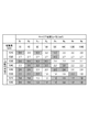
- N 1 , N 2 , N 3 , and L g for obtaining an optimum driving state with respect to the incident light wavelength ⁇ are summarized as shown in FIG.
- the N g black circle shows the plot point N a by white circles.
- the target emission light is calculated assuming a Gaussian-shaped sweep spectrum having a center wavelength of 1060 nm, a light intensity of 20 mW at the center wavelength, and a full width at half maximum of 90 nm.
- the center wavelength, the light intensity at the center wavelength, the full width at half maximum, and the sweep spectrum shape are not limited to this (see Embodiment 4 for the rectangular shape).
- the plurality of gain regions have the same carrier density, but there is a range where the effect can be obtained even if the carrier densities are not the same.
- the non-gain region shows an example in which the carrier density is such that the gain at the incident light wavelength is zero, but it is effective if the gain with respect to the incident light wavelength is equal to or less than zero, and may be driven with zero or reverse bias.
- the non-gain region and the drive system may not be connected, or the electrode may not be formed in the non-gain region.
- the wavelength in the optimum driving state is 1010, 1040, 1080 nm
- the wavelength is not limited to this wavelength as long as it is within the target wavelength range.
- the setting is made to vary within the target wavelength range.
- the electrode shows an example of a three-electrode configuration, but the effect of the present invention can be obtained if there are two or more (see Embodiment 2 for the two-electrode configuration).
- a configuration may be adopted in which a large number of electrodes having a short length (for example, 10 ⁇ m) are arranged. By doing so, it becomes possible to approach the gain length for achieving a more optimal driving state (refer to Embodiment 3 for the electrode configuration capable of finely setting the gain region). However, with this configuration, absorption in the non-electrode region increases, and it may be difficult to control the electrode configuration and driving state.
- the same effect can be obtained even when there are more electrodes if the driving state is substantially the same.
- L a will may be designed long. However, if the length is increased, the amount of unnecessary ASE light increases, so it is desirable to shorten it as much as possible.
- SOA gain spectrum control method Another configuration example of the SOA and the wavelength swept light source according to the present embodiment will be described.
- the wavelength swept light source 102 is driven, and the emitted light is demultiplexed by a beam splitter (not shown). A part of the demultiplexed light is detected as a monitor light by a line sensor (not shown), and a signal corresponding to the center wavelength of the monitor light is transmitted to the control unit 105. Then, current is injected into each electrode of the SOA 104 based on the signal. With such a configuration, the SOA 104 can be controlled to a gain spectrum corresponding to the wavelength of light actually emitted from the wavelength swept light source.
- the same signal is sent from the waveform generator 101 to a voltage amplifier (not shown) for controlling the MEMS drive of the wavelength swept light source 102 and the current controller 105 of the SOA, and the SOA is a gain spectrum corresponding to the light emitted from the wavelength swept light source. You may control to become.
- the table also shows the correspondence between the time variation of the wavelength of the light emitted from the wavelength swept light source 102 and the current value that needs to be injected into the SOA in order to perform optical amplification suitable for each wavelength of the emitted light. It is also possible to have a memory (not shown) stored as
- the optical amplification method according to the present embodiment uses the semiconductor optical amplifier as described in the first embodiment. Specifically, at least one of the electrode layers constituting the semiconductor optical amplifier has an electrode group including two or more electrodes separated in the waveguide direction of the optical waveguide of the semiconductor optical amplifier. .
- the optical amplification method in this embodiment has at least the following three steps.
- the amplification step (3) by using two or more electrodes of the semiconductor optical amplifier, current is independently injected into a plurality of different regions in the active layer of the semiconductor optical amplifier, and according to the wavelength of incident light, Changing the light amplification factor.
- the amplification step preferably includes a step of changing the gain length according to the wavelength of the incident light.
- the amplification step preferably includes a step of shortening the gain length as the wavelength of incident light is shorter.
- the amplification step has a step of injecting current into the active layer so that the carrier density of the active layer increases as the wavelength of incident light is shorter.
- the amplification step has a step of shortening the gain region as the wavelength of incident light is shorter.
- Embodiment 2 of the present invention is shown below.
- FIG. 13 shows a top view of the element configuration of the SOA in the present embodiment.
- the present embodiment is the same as the first embodiment except for the electrode configuration and the driving state. Therefore, only differences from the first embodiment will be described.
- the upper electrode layer has an electrode group including two electrodes. Therefore, the derivation of the optimum driving state and the actual driving can be executed more easily.
- the electrode length is designed so that the optimum driving state can be achieved with respect to, for example, 1020 and 1070 nm.
- the optimum driving state is derived by the method shown in the first embodiment, and N 1 , N 2 , and L g for obtaining the optimum driving state with respect to the incident light wavelength ⁇ are summarized as shown in FIG.
- the N g black circle shows the plot point N a by white circles.
- Embodiment 3 of the present invention is shown below.
- FIG. 16 shows the element configuration of the SOA in the present embodiment.
- the present embodiment is the same as the first embodiment except for the electrode configuration and the driving state. Therefore, only differences from the first embodiment will be described.
- This embodiment is characterized by an electrode configuration in which the length of the electrode is regularly changed. By doing so, the gain length and the non-gain length due to the combination can be adjusted with a higher degree of freedom than in the first embodiment.
- the length of each electrode is set so that a gain length for obtaining an optimum driving state can be obtained with respect to a certain incident light wavelength.
- the optimum driving state is obtained at other wavelengths. Therefore, it cannot be a gain length.
- L 1 to L 8 are set to 20, 40, 80, 160, 320, 640, 1280, 1090 ⁇ m (in no particular order).
- the gain length for achieving the optimum driving state can be obtained at the incident light wavelength of 1080 nm where the gain length for achieving the optimum driving state is the largest value.
- the difference between the gain length for achieving the optimum driving state at each incident light wavelength and the actual gain length can be suppressed to less than 10 ⁇ m.
- the optimum driving state is derived by the method shown in the first embodiment, and the lengths and carrier densities of the respective electrode regions for obtaining the optimum driving state with respect to the incident light wavelength are summarized as shown in FIG.
- the same effect can be obtained even if the length of each electrode described above and the driving state corresponding to the electrode are interchanged.
- the colored carrier density represents the carrier density in the non-gain region.
- the minimum unit of the electrode is 20 ⁇ m
- the same effect as in the present embodiment can be obtained with values of 10 ⁇ m, 50 ⁇ m, and 100 ⁇ m.
- the thickness is less than 10 ⁇ m, the absorption in the non-electrode region increases, and it may be difficult to control the electrode configuration and the driving state.
- Embodiment 4 of the present invention will be described below.
- the present embodiment is the same as the first embodiment except for the target emission light. Therefore, only differences from the first embodiment will be described. Therefore, the sample configuration is as shown in FIG. 3, but the length and driving state of the electrodes are different from those of the first embodiment.
- the target emission light in the present embodiment assumes a rectangular sweep spectrum (FIG. 18) having a light intensity of 20 mW at a wavelength of 1010 to 1080 nm.
- the method for deriving the optimum driving state is as described in the first embodiment.
- the electrode length is designed so that the optimum driving state can be achieved with respect to 1010, 1040, 1080 nm, for example.
- FIG. 19 shows the results of determining L g , N g , and N a for achieving the optimum driving state with respect to the target wavelength range of 1010 to 1080 nm. Furthermore, FIG. 20 shows the N 1 , N 2 , N 3 , and L g for deriving the optimum driving state and setting the optimum driving state for the incident light wavelength ⁇ .
- the N g black circle shows the plot point N a by white circles.
- Embodiment 5 of the present invention will be described below.
- the OCT apparatus includes a light source unit 301 (MEMS-VCSEL) in which the emitted optical frequency is swept, an optical amplifier (SOA) 302 that performs optical output increase and sweep spectrum shape control, and an isolator 303 therebetween. Then, an interference unit 304 that generates interference light, a signal output unit 305 that receives the interference light and outputs an interference signal, and an acquisition unit 306 that acquires information on an object (subject) based on the interference signal Have. Further, the OCT apparatus has a measurement arm (irradiation optical system) 307 and a reference arm (reference optical system) 308.
- the interference unit 304 includes two couplers 310 and 311.
- the coupler 310 branches the light emitted from the light source into irradiation light for irradiating the subject 312 and reference light.
- the irradiation light is irradiated to the subject 312 via the measurement arm 307. More specifically, the irradiation light incident on the measurement arm 307 is adjusted in polarization state by the polarization controller 313 and then emitted from the collimator 314 as spatial light. Thereafter, the irradiated light is irradiated to the subject 312 via the X-axis scanner 315, the Y-axis scanner 316, and the focus lens 317.
- the X-axis scanner 315 and the Y-axis scanner 316 are scanning units having a function of scanning the subject 312 with irradiation light.
- the irradiation position of the irradiation light on the subject 312 is changed by the scanning unit.
- the back scattered light (reflected light) from the subject 312 is emitted from the measurement arm 307 via the focus lens 317, the Y-axis scanner 316, the X-axis scanner 315, the collimator 314, and the polarization controller 313 again.
- the light enters the coupler 311 via the coupler 310.
- the interference unit 304, the measurement arm 307, and the reference arm 308 can be collectively referred to as an interference optical system.
- the interference optical system is a Mach-Zehnder type, but may be a Michelson type.
- the reference light enters the coupler 311 via the reference arm 308. More specifically, the reference light incident on the reference arm 308 is emitted from the collimator 319 as spatial light after its polarization state is adjusted by the polarization controller 318. Thereafter, the reference light passes through the dispersion compensation glass 320, the optical path length adjustment optical system 321, and the dispersion adjustment prism pair 322, enters the optical fiber through the collimator lens 323, exits from the reference arm 308, and enters the coupler 311.
- the signal output unit 305 includes a differential detector 324 and an A / D converter 325.
- the differential detector 324 detects the interference light that is demultiplexed immediately after the interference light is generated by the coupler 311.
- the interference signal converted into an electrical signal by the differential detector 324 is converted into a digital signal by the A / D converter 325.
- the digital signal is sent to the information acquisition unit 306, and frequency analysis such as Fourier transform is performed on the digital signal, whereby information on the subject 312 is obtained.
- Information about the obtained subject 312 is displayed as a tomographic image by the display unit 326.
- the sampling timing of the interference light is performed at equal optical frequency (equal wave number) intervals based on a k clock signal transmitted from a k clock generation unit 327 provided outside the light source.
- a coupler 309 is provided to branch a part of the light emitted from the light source to the k clock generation unit 327.
- k clock generation unit 327 and the coupler 309 may be incorporated in the light source 301 or the SOA 302.
- A-scan Acquiring information about a tomography in the depth direction of the subject 312 is called A-scan.
- the information about the tomography of the subject 312 in the direction orthogonal to the A-scan is orthogonal to the scanning direction of B-scan, and further, the A-scan and B-scan. Scanning in this direction is called C-scan.
- C-scan This is because, when acquiring a three-dimensional tomographic image, when performing two-dimensional raster scanning in the fundus, the high-speed scanning direction is B-scan, and the low-speed scanning direction in which B-scan is arranged in the orthogonal direction is C- Call it scan.
- a two-dimensional tomographic image can be obtained by performing A-scan and B-scan, and a three-dimensional tomographic image can be obtained by performing A-scan, B-scan and C-scan.
- B-scan and C-scan are performed by the X-axis scanner 315 and the Y-axis scanner 316 described above.
- the X-axis scanner 315 and the Y-axis scanner 316 are composed of deflection mirrors that are arranged so that their rotation axes are orthogonal to each other.
- the X-axis scanner 315 performs scanning in the X-axis direction
- the Y-axis scanner 316 performs scanning in the Y-axis direction.
- the X-axis direction and the Y-axis direction are directions perpendicular to the surface normal of the subject and perpendicular to each other.
- the line scanning direction such as B-scan and C-scan may not coincide with the X-axis direction or the Y-axis direction. Therefore, the B-scan and C-scan line scanning directions can be appropriately determined according to a two-dimensional tomographic image or a three-dimensional tomographic image to be imaged.
- a characteristic of this embodiment is the SOA.
- the SOA of the present invention described in the above embodiment is used, the ASE light can be reduced while controlling the sweep spectrum shape of the MEMS-VCSEL, so that high-resolution tomographic image information can be obtained. Will be advantageous to get.
- This OCT apparatus is mainly useful for tomographic imaging in ophthalmology.
Landscapes
- Physics & Mathematics (AREA)
- General Physics & Mathematics (AREA)
- Health & Medical Sciences (AREA)
- Life Sciences & Earth Sciences (AREA)
- Condensed Matter Physics & Semiconductors (AREA)
- Electromagnetism (AREA)
- Optics & Photonics (AREA)
- General Health & Medical Sciences (AREA)
- Molecular Biology (AREA)
- Veterinary Medicine (AREA)
- Engineering & Computer Science (AREA)
- Biomedical Technology (AREA)
- Heart & Thoracic Surgery (AREA)
- Medical Informatics (AREA)
- Biophysics (AREA)
- Surgery (AREA)
- Animal Behavior & Ethology (AREA)
- Radiology & Medical Imaging (AREA)
- Public Health (AREA)
- Ophthalmology & Optometry (AREA)
- Nuclear Medicine, Radiotherapy & Molecular Imaging (AREA)
- Analytical Chemistry (AREA)
- Biochemistry (AREA)
- Immunology (AREA)
- Pathology (AREA)
- Chemical & Material Sciences (AREA)
- Geometry (AREA)
- Semiconductor Lasers (AREA)
- Investigating Or Analysing Materials By Optical Means (AREA)
- Eye Examination Apparatus (AREA)
Abstract
L'invention porte sur un amplificateur optique qui comporte un corps stratifié qui comprend deux couches d'électrodes et une couche active qui est disposée entre les couches d'électrodes. Le corps stratifié comporte un guide d'ondes dans lequel la lumière est guidée dans la direction plane de la couche active. La lumière qui est incidente sur le corps stratifié passe par le guide d'ondes et est amplifiée et émise par un côté surface d'extrémité dans la direction plane du corps stratifié. Au moins une des deux couches d'électrodes comporte un groupe d'électrodes qui comprend au moins deux électrodes qui sont disposées de manière à être séparées dans la direction de guidage d'ondes du guide d'ondes. L'amplificateur optique utilise lesdites deux électrodes pour injecter indépendamment du courant dans une pluralité de zones différentes de la couche active, et peut ainsi modifier le facteur d'amplification de la lumière incidente en fonction de la longueur d'onde de la lumière incidente. La présente invention procure un amplificateur optique qui peut réduire la lumière d'émission spontanée amplifiée (ASE), qui comprend de la lumière de longueurs d'onde non nécessaires, tout en atteignant une intensité de sortie optique suffisante à une longueur d'onde nécessaire.
Priority Applications (1)
| Application Number | Priority Date | Filing Date | Title |
|---|---|---|---|
| US16/170,612 US20190059717A1 (en) | 2016-04-28 | 2018-10-25 | Optical amplifier, optical coherence tomography including optical amplifier, and optical amplification method using optical amplifier |
Applications Claiming Priority (2)
| Application Number | Priority Date | Filing Date | Title |
|---|---|---|---|
| JP2016091615A JP2017199877A (ja) | 2016-04-28 | 2016-04-28 | 光増幅器、それを備える光干渉断層計、及び光増幅器を用いた光増幅方法 |
| JP2016-091615 | 2016-04-28 |
Related Child Applications (1)
| Application Number | Title | Priority Date | Filing Date |
|---|---|---|---|
| US16/170,612 Continuation US20190059717A1 (en) | 2016-04-28 | 2018-10-25 | Optical amplifier, optical coherence tomography including optical amplifier, and optical amplification method using optical amplifier |
Publications (1)
| Publication Number | Publication Date |
|---|---|
| WO2017188364A1 true WO2017188364A1 (fr) | 2017-11-02 |
Family
ID=60159954
Family Applications (1)
| Application Number | Title | Priority Date | Filing Date |
|---|---|---|---|
| PCT/JP2017/016689 Ceased WO2017188364A1 (fr) | 2016-04-28 | 2017-04-27 | Amplificateur optique, dispositif de tomographie de cohérence optique comprenant l'amplificateur optique, et procédé d'amplification optique utilisant l'amplificateur optique |
Country Status (3)
| Country | Link |
|---|---|
| US (1) | US20190059717A1 (fr) |
| JP (1) | JP2017199877A (fr) |
| WO (1) | WO2017188364A1 (fr) |
Cited By (1)
| Publication number | Priority date | Publication date | Assignee | Title |
|---|---|---|---|---|
| CN114764165A (zh) * | 2021-01-15 | 2022-07-19 | 三星电子株式会社 | 光隔离器和包括其的光子集成电路 |
Families Citing this family (1)
| Publication number | Priority date | Publication date | Assignee | Title |
|---|---|---|---|---|
| DE112018004478B4 (de) | 2017-10-13 | 2025-03-27 | Rohm Co., Ltd. | Elektronikkomponente |
Citations (7)
| Publication number | Priority date | Publication date | Assignee | Title |
|---|---|---|---|---|
| JPH0645678A (ja) * | 1992-03-17 | 1994-02-18 | Nec Corp | 半導体光増幅器の光出力パワー一定化方法及び装置 |
| US20030039425A1 (en) * | 2001-08-23 | 2003-02-27 | Robert Stoddard | Integrated optical switch/amplifier with modulation cpabilities |
| JP2003124578A (ja) * | 2001-10-09 | 2003-04-25 | Nippon Telegr & Teleph Corp <Ntt> | 半導体光増幅素子 |
| JP2007184557A (ja) * | 2005-12-05 | 2007-07-19 | Fujifilm Corp | 半導体発光素子および該素子を備えた光源装置および光断層画像化装置 |
| JP2009049280A (ja) * | 2007-08-22 | 2009-03-05 | Sharp Corp | 半導体光増幅素子及び脈波計測装置 |
| JP2014082485A (ja) * | 2012-09-28 | 2014-05-08 | Canon Inc | 光源及び前記光源を用いた光干渉断層撮像装置 |
| JP2016027333A (ja) * | 2014-06-30 | 2016-02-18 | キヤノン株式会社 | 光干渉断層計、面発光レーザ |
-
2016
- 2016-04-28 JP JP2016091615A patent/JP2017199877A/ja active Pending
-
2017
- 2017-04-27 WO PCT/JP2017/016689 patent/WO2017188364A1/fr not_active Ceased
-
2018
- 2018-10-25 US US16/170,612 patent/US20190059717A1/en not_active Abandoned
Patent Citations (7)
| Publication number | Priority date | Publication date | Assignee | Title |
|---|---|---|---|---|
| JPH0645678A (ja) * | 1992-03-17 | 1994-02-18 | Nec Corp | 半導体光増幅器の光出力パワー一定化方法及び装置 |
| US20030039425A1 (en) * | 2001-08-23 | 2003-02-27 | Robert Stoddard | Integrated optical switch/amplifier with modulation cpabilities |
| JP2003124578A (ja) * | 2001-10-09 | 2003-04-25 | Nippon Telegr & Teleph Corp <Ntt> | 半導体光増幅素子 |
| JP2007184557A (ja) * | 2005-12-05 | 2007-07-19 | Fujifilm Corp | 半導体発光素子および該素子を備えた光源装置および光断層画像化装置 |
| JP2009049280A (ja) * | 2007-08-22 | 2009-03-05 | Sharp Corp | 半導体光増幅素子及び脈波計測装置 |
| JP2014082485A (ja) * | 2012-09-28 | 2014-05-08 | Canon Inc | 光源及び前記光源を用いた光干渉断層撮像装置 |
| JP2016027333A (ja) * | 2014-06-30 | 2016-02-18 | キヤノン株式会社 | 光干渉断層計、面発光レーザ |
Cited By (1)
| Publication number | Priority date | Publication date | Assignee | Title |
|---|---|---|---|---|
| CN114764165A (zh) * | 2021-01-15 | 2022-07-19 | 三星电子株式会社 | 光隔离器和包括其的光子集成电路 |
Also Published As
| Publication number | Publication date |
|---|---|
| US20190059717A1 (en) | 2019-02-28 |
| JP2017199877A (ja) | 2017-11-02 |
Similar Documents
| Publication | Publication Date | Title |
|---|---|---|
| USRE41633E1 (en) | Light source for swept source optical coherence tomography based on cascaded distributed feedback lasers with engineered band gaps | |
| JP2017175157A (ja) | 掃引源光干渉断層撮影システム用の波長同調型垂直キャビティ面発光レーザー | |
| JP2009283736A (ja) | 光半導体素子および光半導体素子を用いた光干渉断層画像装置 | |
| JP2015103740A (ja) | 面発光レーザ、およびそれを用いた光干渉断層計 | |
| US7944567B2 (en) | Semiconductor light emitting element, light source using the semiconductor light emitting element, and optical tomography imaging apparatus | |
| JP2009049310A (ja) | 半導体レーザ、バイオイメージングシステム、顕微鏡、光ディスク装置、光ピックアップ、加工装置および内視鏡 | |
| JP2009049123A (ja) | 光半導体素子、該光半導体素子を用いた波長可変光源および光断層画像取得装置 | |
| US20130242310A1 (en) | Light source device including super luminescent diodes, method of driving the same, and optical tomography imaging apparatus | |
| JP2015026645A (ja) | 面発光レーザおよび光干渉断層計 | |
| JP6253326B2 (ja) | 光源及び前記光源を用いた光干渉断層撮像装置 | |
| JP2007184557A (ja) | 半導体発光素子および該素子を備えた光源装置および光断層画像化装置 | |
| US10290994B2 (en) | Laser device, information acquisition device, and imaging system | |
| US20150085295A1 (en) | Light emitting device and optical coherence tomography apparatus including same as light source | |
| US9124070B2 (en) | Superluminescent diode and optical coherence tomography apparatus including the superluminescent diode | |
| WO2017188364A1 (fr) | Amplificateur optique, dispositif de tomographie de cohérence optique comprenant l'amplificateur optique, et procédé d'amplification optique utilisant l'amplificateur optique | |
| JP2008270585A (ja) | 光半導体素子、該光半導体素子を用いた波長可変光源および光断層画像取得装置 | |
| JP6608203B2 (ja) | 面発光レーザ、情報取得装置及び撮像装置 | |
| JP2015233127A (ja) | 面発光レーザ、レーザアレイ、光源装置、情報取得装置及び光干渉断層計 | |
| JP6282094B2 (ja) | 面発光レーザ、およびそれを用いた光干渉断層計 | |
| JP2008192731A (ja) | 半導体発光素子および該素子を備えた光断層画像化装置 | |
| JP6650961B2 (ja) | 面発光レーザ、およびそれを用いた光干渉断層計 | |
| JP2017098303A (ja) | レーザ装置及び撮像装置 | |
| JP2017143201A (ja) | 光源装置及び情報取得装置 | |
| CN106449898A (zh) | 发光装置及其控制方法和光学相干断层成像设备 | |
| JP2015194496A (ja) | 光源システム、及び前記光源システムを用いた光干渉断層計 |
Legal Events
| Date | Code | Title | Description |
|---|---|---|---|
| NENP | Non-entry into the national phase |
Ref country code: DE |
|
| 121 | Ep: the epo has been informed by wipo that ep was designated in this application |
Ref document number: 17789646 Country of ref document: EP Kind code of ref document: A1 |
|
| 122 | Ep: pct application non-entry in european phase |
Ref document number: 17789646 Country of ref document: EP Kind code of ref document: A1 |