WO2017195591A1 - Convertisseur cc-cc bidirectionnel - Google Patents
Convertisseur cc-cc bidirectionnel Download PDFInfo
- Publication number
- WO2017195591A1 WO2017195591A1 PCT/JP2017/016473 JP2017016473W WO2017195591A1 WO 2017195591 A1 WO2017195591 A1 WO 2017195591A1 JP 2017016473 W JP2017016473 W JP 2017016473W WO 2017195591 A1 WO2017195591 A1 WO 2017195591A1
- Authority
- WO
- WIPO (PCT)
- Prior art keywords
- input
- unit
- output
- switching
- converter
- Prior art date
- Legal status (The legal status is an assumption and is not a legal conclusion. Google has not performed a legal analysis and makes no representation as to the accuracy of the status listed.)
- Ceased
Links
Images


Classifications
-
- H—ELECTRICITY
- H02—GENERATION; CONVERSION OR DISTRIBUTION OF ELECTRIC POWER
- H02M—APPARATUS FOR CONVERSION BETWEEN AC AND AC, BETWEEN AC AND DC, OR BETWEEN DC AND DC, AND FOR USE WITH MAINS OR SIMILAR POWER SUPPLY SYSTEMS; CONVERSION OF DC OR AC INPUT POWER INTO SURGE OUTPUT POWER; CONTROL OR REGULATION THEREOF
- H02M3/00—Conversion of DC power input into DC power output
- H02M3/02—Conversion of DC power input into DC power output without intermediate conversion into AC
- H02M3/04—Conversion of DC power input into DC power output without intermediate conversion into AC by static converters
- H02M3/10—Conversion of DC power input into DC power output without intermediate conversion into AC by static converters using discharge tubes with control electrode or semiconductor devices with control electrode
- H02M3/145—Conversion of DC power input into DC power output without intermediate conversion into AC by static converters using discharge tubes with control electrode or semiconductor devices with control electrode using devices of a triode or transistor type requiring continuous application of a control signal
- H02M3/155—Conversion of DC power input into DC power output without intermediate conversion into AC by static converters using discharge tubes with control electrode or semiconductor devices with control electrode using devices of a triode or transistor type requiring continuous application of a control signal using semiconductor devices only
Definitions
- the present invention relates to a bidirectional DC-DC converter that performs bidirectional power conversion between two input / output units.
- Patent Document 1 discloses an insulated bidirectional DC-DC converter. This bidirectional DC-DC converter switches from the input side of the DC-DC converter by switching the voltage detection circuit and the drive circuit according to the direction of power supply without changing the connection on the input side and the connection on the output side. The power supply to the output side and the power supply from the output side to the input side are enabled.
- the bidirectional DC-DC converter of Patent Document 1 immediately after the direction of power supply is switched, the control becomes unstable and there is a risk of causing an abnormal operation. For example, when the output voltage is higher than the input voltage, the bidirectional DC-DC converter performs a step-up operation from the input side to the output side. At this time, when the power supply direction is switched, the output side is changed to the input side. Although the step-down operation should be performed, the step-up operation is maintained immediately after switching, and there is a risk of supplying excessive power.
- an object of the present invention is to provide a bidirectional DC-DC converter that performs stable operation.
- a bidirectional DC-DC converter includes a first input / output unit, a second input / output unit, and a converter unit that performs bidirectional power conversion between the first input / output unit and the second input / output unit.
- a switching signal receiving unit that receives a switching signal for switching the power conversion direction, a first input / output voltage detecting unit that detects an input / output voltage for the first input / output unit, and an input / output voltage for the second input / output unit Based on the second input / output voltage detection unit for detecting the switching signal, the switching signal received by the switching signal receiving unit, and the detection result by the first input / output voltage detection unit or the second input / output voltage detection unit,
- a switching control unit that performs switching control of the converter unit, and the switching control unit stops switching control when the switching signal receiving unit receives the switching signal, and performs switching control after a predetermined period of time has elapsed.
- the switching control when the switching signal is received, the switching control is stopped for a predetermined period, for example, until the electric charge stored in the capacitor included in the switching control unit is discharged, thereby stabilizing the control and converting the power.
- the direction can be switched.
- the bidirectional DC-DC converter includes an error amplification unit that compares a detection result of the first input / output voltage detection unit or the second input / output voltage detection unit with a reference value, and the error amplification unit is an integration element
- the switching control unit may perform switching control based on an output of the error amplifying unit.
- the stability and responsiveness can be improved by providing a phase compensation circuit. Further, the deviation between the output voltage and the reference value can be brought close to zero by the integration element included in the phase compensation circuit.
- the phase compensation circuit may include a differential element.
- the response speed can be increased by the differential element included in the phase compensation circuit.
- the converter unit may be an H bridge converter.
- the control after switching the power conversion direction is stabilized by stopping the switching control for a predetermined period, for example, until the electric charge stored in the capacitor included in the switching control unit is discharged. be able to.
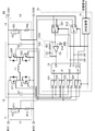
- FIG. 1 is a circuit diagram of a bidirectional DC-DC converter according to an embodiment.
- FIG. 2 is a timing chart for explaining the operation of the switching control unit when the control mode is switched.
- FIG. 3 is a circuit diagram of another example of a bidirectional DC-DC converter.
- FIG. 1 is a circuit diagram of a bidirectional DC-DC converter 1 according to this embodiment.
- the bidirectional DC-DC converter 1 includes a pair of input / output terminals IO11 and IO12, and a pair of input / output terminals IO21 and IO22.
- the input / output terminal IO11 and the input / output terminal IO12 are examples of the “first input / output unit” according to the invention.
- the input / output terminal IO21 and the input / output terminal IO22 are examples of the “second input / output unit” according to the present invention.
- the bidirectional DC-DC converter 1 is driven in one of four control modes.
- the bidirectional DC-DC converter 1 boosts the voltage input from the input / output terminal IO11 and the input / output terminal IO12 and outputs the boosted voltage from the input / output terminal IO21 and the input / output terminal IO22.
- the bidirectional DC-DC converter 1 steps down the voltage input from the input / output terminal IO11 and the input / output terminal IO12 and outputs the voltage from the input / output terminal IO21 and the input / output terminal IO22.
- the bidirectional DC-DC converter 1 boosts the voltage input from the input / output terminal IO21 and the input / output terminal IO22 and outputs the boosted voltage from the input / output terminal IO11 and the input / output terminal IO22.
- the bidirectional DC-DC converter 1 steps down the voltage input from the input / output terminal IO21 and the input / output terminal IO22 and outputs the voltage from the input / output terminal IO11 and the input / output terminal IO22.
- the bidirectional DC-DC converter 1 can bidirectionally convert power between the input / output terminal IO11 and the input / output terminal IO12 and the input / output terminal IO21 and the input / output terminal IO22.
- the bidirectional DC-DC converter 1 Power can be supplied from the secondary battery to the load, and power can be supplied from the power source to the secondary battery to charge the secondary battery.
- the converter unit 10 is connected between the input / output terminals IO11 and IO12 and the input / output terminals IO21 and IO22.
- the converter unit 10 includes a capacitor C1, a series circuit of a switch element Q11 and a switch element Q12, a series circuit of a switch element Q21 and a switch element Q22, a capacitor C2, and an inductor L1.
- the capacitor C1 and the series circuit of the switch element Q11 and the switch element Q12 are connected between the input / output terminal IO11 and the input / output terminal IO12, respectively.
- the switch element Q11 and the switch element Q12 are MOS-FETs.
- Capacitor C2 and a series circuit of switch element Q21 and switch element Q22 are connected between input / output terminal IO21 and input / output terminal IO22, respectively.
- the switch element Q21 and the switch element Q22 are MOS-FETs.
- Inductor L1 is connected between a connection point between switch elements Q11 and Q12 and a connection point between switch elements Q21 and Q22.
- the bidirectional DC-DC converter 1 is a so-called H-bridge circuit having a symmetrical circuit configuration with the inductor L1 as the center. Since the H bridge circuit is non-insulated, an increase in size of the bidirectional DC-DC converter 1 can be suppressed.
- the switching control of the converter unit 10 will be described later.
- the voltage detection circuit 11 is connected between the input / output terminal IO11 and the input / output terminal IO12.
- the voltage detection circuit 11 is a voltage dividing circuit of a resistor R11 and a resistor R12.
- the voltage detection circuit 11 detects the voltage V1 with respect to the input / output terminal IO11 and the input / output terminal IO12.
- the voltage V1 is the input voltage of the bidirectional DC-DC converter 1.
- the voltage V1 is the output voltage of the bidirectional DC-DC converter 1.
- the voltage detection circuit 11 is an example of the “first input / output voltage detection unit” according to the present invention.
- the voltage detection circuit 12 is connected between the input / output terminal IO21 and the input / output terminal IO22.
- the voltage detection circuit 12 is a voltage dividing circuit of a resistor R21 and a resistor R22.
- the voltage detection circuit 12 detects the voltage V2 with respect to the input / output terminal IO21 and the input / output terminal IO22.
- the voltage V2 is the input voltage of the bidirectional DC-DC converter 1.
- the voltage V2 is the output voltage of the bidirectional DC-DC converter 1.
- the voltage detection circuit 12 is an example of the “second input / output voltage detection unit” according to the present invention.
- the bidirectional DC-DC converter 1 includes a control unit 13.
- the control unit 13 includes a SW switching unit 14, an error amplification unit 15, and a switching control unit 16.
- the control unit 13 includes a switch S11, a switch S12, a switch S21, a switch S22, a switch S23, and a switch S24.
- the SW switch 14 receives a switching signal from the outside.
- the switching signal is a signal for switching the control mode of the bidirectional DC-DC converter 1.
- the SW switching unit 14 switches the switches S11, S12, and S21 to S24. Further, the SW switching unit 14 outputs a received switching signal to the switching control unit 16.
- the SW switching unit 14 is an example of the “switching signal receiving unit” according to the present invention.
- Switch S11 and switch S12 are single-pole double-throw switches that output one of two inputs. Output voltages from the voltage detection circuit 11 and the voltage detection circuit 12 are input to the switch S11 and the switch S12, respectively, and one of them is output. When the input / output terminal IO11 and the input / output terminal IO12 are on the input side, the switch S11 and the output voltage of the voltage detection circuit 12 are output from the switch S11, and the output voltage of the voltage detection circuit 11 is output from the switch S12. Switch S12 is switched. That is, according to the control mode of the bidirectional DC-DC converter 1, the output voltage of the bidirectional DC-DC converter 1 is output from the switch S11, and the input voltage of the bidirectional DC-DC converter 1 is output from the switch S12. As described above, the switch S11 and the switch S12 are switched.
- the output of the switch S11 is connected to the error amplifying unit 15 and the terminal Vo of the switching control unit 16, respectively.
- the terminal Vo is a terminal for inputting the output voltage of the bidirectional DC-DC converter 1.
- the output of the switch S12 is connected to the terminal Vi of the switching control unit 16.
- the terminal Vi is a terminal for inputting the input voltage of the bidirectional DC-DC converter 1.
- the switching control unit 16 determines a step-down or step-up control mode based on the input voltage and output voltage of the bidirectional DC-DC converter 1 input to the terminal Vi and the terminal Vo.
- the error amplification unit 15 compares the output voltage of the bidirectional DC-DC converter 1, that is, the output voltage of the voltage detection circuit 11 or the voltage detection circuit 12, with the reference voltage Vref.
- the output of the error amplifying unit 15 is connected to the CP (COMP) terminal of the switching control unit 16.
- the switching control unit 16 determines the switching duty of the converter unit 10 based on the output of the error amplification unit 15 and generates a PWM-modulated gate signal.
- the output voltage of the bidirectional DC-DC converter 1 is input to one error amplifying unit 15. Then, the output voltage of the bidirectional DC-DC converter 1 is compared with the same reference voltage Vref.
- the reference voltage may be changed by an external command or a voltage of a secondary battery connected to input / output.
- the error amplifier 15 includes an error amplifier 151 and a phase compensation circuit 152.
- the phase compensation circuit 152 is configured by connecting a capacitor C3 and a resistor R3 in series. By providing the phase compensation circuit 152, stability and responsiveness can be improved.
- the capacitor C3 is an example of the “integration element” according to the present invention.
- the reference voltage Vref is input to the non-inverting input terminal of the error amplifier 151.
- the output of the switch S11 is connected to the inverting input terminal of the error amplifier 151. That is, the output voltage from the voltage detection circuit 11 or the voltage detection circuit 12 is input to the inverting input terminal of the error amplifier 151.
- the phase compensation circuit 152 is a circuit for performing phase compensation of the negative feedback loop, and is connected between the output terminal and the inverting input terminal of the error amplifier 151.
- the switches S21 to S24 are single-pole double-throw switches having one input terminal and two first output terminals and second output terminals.
- the switches S21 to S24 are respectively connected to the terminal HI, the terminal LI, the terminal HO, and the terminal LO of the switching control unit 16 that outputs a gate signal to each switch element of the converter unit 10.
- the input terminal of the switch S21 is connected to the terminal HI of the switching control unit 16.
- the first output terminal of the switch S21 is connected to the gate of the switch element Q11.
- a second output terminal of the switch S21 is connected to the gate of the switch element Q21.
- the input terminal of the switch S22 is connected to the terminal LI of the switching control unit 16.
- the first output terminal of the switch S22 is connected to the gate of the switch element Q12.
- a second output terminal of the switch S22 is connected to the gate of the switch element Q22.
- the input terminal of the switch S23 is connected to the terminal HO of the switching control unit 16.
- the first output terminal of the switch S23 is connected to the gate of the switch element Q21.
- a second output terminal of the switch S23 is connected to the gate of the switch element Q11.
- the input terminal of the switch S24 is connected to the terminal LO of the switching control unit 16.
- the first output terminal of the switch S24 is connected to the gate of the switch element Q22.
- a second output terminal of the switch S24 is connected to the gate of the switch element Q12.
- the switches S21 to S24 are switched by the SW switching unit 14 in accordance with the control mode of the bidirectional DC-DC converter 1.
- the switch S21, the switch S22, the switch S23, and the switch S24 are switched so that the input terminal and the first output terminal are connected. It is done. That is, the terminal HI is connected to the switch element Q11, the terminal LI is connected to the switch element Q12, the terminal HO is connected to the switch element Q21, and the terminal LO is connected to the switch element Q22.
- the switch S21, the switch S22, the switch S23, and the switch S24 are switched so that the input terminal and the second output terminal are connected. That is, the terminal HI is connected to the switch element Q21, the terminal LI is connected to the switch element Q22, the terminal HO is connected to the switch element Q11, and the terminal LO is connected to the switch element Q12.
- the bidirectional DC-DC converter 1 boosts the input voltage from the input / output terminal IO11 and the input / output terminal IO12 and outputs the boosted voltage from the input / output terminal IO21 and the input / output terminal IO22.
- the SW switching unit 14 switches the switch S11 so that the output voltage of the voltage detection circuit 12 is input to the error amplification unit 15.
- the error amplifying unit 15 compares the output voltage of the voltage detection circuit 12 with the reference voltage Vref and outputs it to the switching control unit 16.
- the switching control unit 16 determines the duty ratio of the switching control from the comparison result.
- the switching control unit 16 always turns on the switch element Q11 and always turns off the switch element Q12. Then, the switching control unit 16 turns on and off the switch elements Q21 and Q22 alternately with the determined duty ratio. At this time, the switch element Q21 operates as a synchronous rectifier element.
- the bidirectional DC-DC converter 1 steps down the input voltage from the input / output terminal IO11 and the input / output terminal IO12 and outputs it from the input / output terminal IO21 and the input / output terminal IO22.
- the SW switching unit 14 switches the switch S11 so that the output voltage of the voltage detection circuit 12 is input to the error amplification unit 15.
- the error amplifying unit 15 compares the output voltage of the voltage detection circuit 12 with the reference voltage Vref and outputs it to the switching control unit 16.
- the switching control unit 16 determines the duty ratio of the switching control from the comparison result.
- the switching control unit 16 always turns on the switch element Q21 and always turns off the switch element Q22. Then, the switching control unit 16 turns on and off the switching elements Q11 and Q12 alternately with the determined duty ratio. At this time, the switch element Q12 operates as a synchronous rectifier element.
- the bidirectional DC-DC converter 1 boosts the input voltage from the input / output terminal IO21 and the input / output terminal IO22 and outputs the boosted voltage from the input / output terminal IO11 and the input / output terminal IO12.
- the SW switching unit 14 switches the switch S11 so that the output voltage of the voltage detection circuit 11 is input to the error amplification unit 15.
- the error amplifying unit 15 compares the output voltage of the voltage detection circuit 11 with the reference voltage Vref and outputs the result to the switching control unit 16.
- the switching control unit 16 determines the duty ratio of the switching control from the comparison result.
- the switching control unit 16 always turns on the switch element Q21 and always turns off the switch element Q22. Then, the switching control unit 16 turns on and off the switching elements Q11 and Q12 alternately with the determined duty ratio. At this time, the switch element Q11 operates as a synchronous rectifier element.
- the bidirectional DC-DC converter 1 steps down the input voltage from the input / output terminal IO21 and the input / output terminal IO22 and outputs it from the input / output terminal IO11 and the input / output terminal IO12.
- the SW switching unit 14 switches the switch S11 so that the output voltage of the voltage detection circuit 11 is input to the error amplification unit 15.
- the error amplifying unit 15 compares the output voltage of the voltage detection circuit 11 with the reference voltage Vref and outputs the result to the switching control unit 16.
- the switching control unit 16 determines the duty ratio of the switching control from the comparison result.
- the switching control unit 16 always turns on the switch element Q11 and always turns off the switch element Q12. Then, the switching control unit 16 turns on and off the switch elements Q21 and Q22 alternately with the determined duty ratio. At this time, the switch element Q22 operates as a synchronous rectifier element.
- the bidirectional DC-DC converter 1 can be driven in any one of the first control mode, the second control mode, the third control mode, and the fourth control mode.
- the switching of the power supply direction is performed according to an external switching signal received by the SW switching unit 14.
- the switching signal is notified to the switching control unit 16.
- the switching control unit 16 switches the power supply direction according to the switching signal.
- the switching control unit 16 stops the switching control for a predetermined period.
- FIG. 2 is a timing chart for explaining the operation of the switching control unit 16 when the control mode is switched. In this example, it is assumed that the bidirectional DC-DC converter 1 is driven in the first control mode until time t1.
- the switching control unit 16 performs switching control until time t1 when the SW switching unit 14 receives a switching signal.
- the switching control unit 16 turns off all the switch elements Q11, Q12, Q21, and Q22 and stops the switching control.
- the SW switching unit 14 switches the switch S11 and the like after the time t2 has elapsed from the time t1.
- the switching control unit 16 starts the switching control so that the bidirectional DC-DC converter 1 is driven in the control mode based on the received switching signal when the time t3 has elapsed. To do.
- the capacitor C3 functions as an integration element, so that charge is used as information for the deviation between the output voltage and the reference value to be zero. Is stored. If the direction of power supply is switched in this state, the control becomes unstable due to the accumulated charge, and an abnormal operation such as excessive or insufficient duty may occur. Further, although it is necessary to switch from the step-up operation to the step-down operation, if there is a capacitor on the Vi and Vo lines of the control unit 13 as a parasitic component or intentionally for noise removal, the capacitor is switched after the switching is performed. There is also a possibility that the boosting operation may be continuously performed during a transition period in which the voltage changes.
- the switching control is stopped for a predetermined period Td.
- the predetermined period Td is a period until the switching control is ready to control by switching the direction of power supply.
- the SW switching unit 14 switches the switch S11 and the like after the elapse of time t5 from time t4.
- FIG. 3 is a circuit diagram of another example bidirectional DC-DC converter 1A.
- the error amplifying unit 15A includes a phase compensation circuit 152A.
- the phase compensation circuit 152A has a series circuit of a capacitor C3 and a resistor R3, and the capacitors C4 and C5 constitute a differential element. Capacitors C4 and C5 are connected in parallel to resistors R11 and R21 of voltage detection circuits 11 and 12, respectively. A series circuit of the capacitor C3 and the resistor R3 is connected between the output terminal and the inverting input terminal of the error amplifier 151. By providing the capacitors C4 and C5, the feedback phase can be advanced, so that the response can be improved.
- the bidirectional DC-DC converter 1 has been described as an H-bridge circuit.
- the bidirectional DC-DC converter 1 can be appropriately changed as long as the circuit can perform bidirectional power conversion between two input / output units.
Landscapes
- Engineering & Computer Science (AREA)
- Power Engineering (AREA)
- Dc-Dc Converters (AREA)
Abstract
La présente invention concerne un convertisseur CC-CC bidirectionnel (1) qui comprend : une unité de convertisseur (10) pour effectuer une conversion de puissance bidirectionnelle entre des terminaux d'entrée/de sortie (IO 11, IO 12) et des bornes d'entrée/de sortie (IO 21, IO 22) ; une partie de commutation (SW) (14) pour recevoir un signal de commutation pour commuter la direction de conversion de puissance ; un circuit de détection de tension (11) et un circuit de détection de tension (12) pour détecter des tensions d'entrée/de sortie ; et une unité de commande de commutation (16) pour effectuer une commande de commutation de l'unité de convertisseur (10) sur la base du signal de commutation reçu par la partie de commutation (SW) (14) et d'un résultat de détection du circuit de détection de tension (11) ou du circuit de détection de tension (12). L'unité de commande de commutation (16) arrête la commande de commutation lorsque le signal de commutation est reçu et reprend la commande de commutation après qu'une période de temps s'est écoulée.
Applications Claiming Priority (2)
| Application Number | Priority Date | Filing Date | Title |
|---|---|---|---|
| JP2016-096694 | 2016-05-13 | ||
| JP2016096694 | 2016-05-13 |
Publications (1)
| Publication Number | Publication Date |
|---|---|
| WO2017195591A1 true WO2017195591A1 (fr) | 2017-11-16 |
Family
ID=60266975
Family Applications (1)
| Application Number | Title | Priority Date | Filing Date |
|---|---|---|---|
| PCT/JP2017/016473 Ceased WO2017195591A1 (fr) | 2016-05-13 | 2017-04-26 | Convertisseur cc-cc bidirectionnel |
Country Status (1)
| Country | Link |
|---|---|
| WO (1) | WO2017195591A1 (fr) |
Cited By (1)
| Publication number | Priority date | Publication date | Assignee | Title |
|---|---|---|---|---|
| CN107979168A (zh) * | 2017-12-22 | 2018-05-01 | 厦门科华恒盛股份有限公司 | 一种数据中心不间断供电系统 |
Citations (7)
| Publication number | Priority date | Publication date | Assignee | Title |
|---|---|---|---|---|
| JPH06269162A (ja) * | 1993-03-11 | 1994-09-22 | Hitachi Lighting Ltd | 電源装置 |
| JP2003052170A (ja) * | 2001-08-03 | 2003-02-21 | Texas Instr Japan Ltd | Dc−dcコンバータ |
| JP2004343855A (ja) * | 2003-05-14 | 2004-12-02 | Taiyo Yuden Co Ltd | 電源装置 |
| WO2007125949A1 (fr) * | 2006-04-27 | 2007-11-08 | Panasonic Corporation | Convertisseur cc-cc bidirectionnel |
| JP2007325478A (ja) * | 2006-06-05 | 2007-12-13 | Torex Device Co Ltd | スイッチング電源回路 |
| JP2014093910A (ja) * | 2012-11-06 | 2014-05-19 | Nippon Steel & Sumikin Texeng Co Ltd | 二次電池用双方向電源装置及びその制御方法 |
| JP2015162951A (ja) * | 2014-02-27 | 2015-09-07 | 株式会社 日立産業制御ソリューションズ | 双方向コンバータ |
-
2017
- 2017-04-26 WO PCT/JP2017/016473 patent/WO2017195591A1/fr not_active Ceased
Patent Citations (7)
| Publication number | Priority date | Publication date | Assignee | Title |
|---|---|---|---|---|
| JPH06269162A (ja) * | 1993-03-11 | 1994-09-22 | Hitachi Lighting Ltd | 電源装置 |
| JP2003052170A (ja) * | 2001-08-03 | 2003-02-21 | Texas Instr Japan Ltd | Dc−dcコンバータ |
| JP2004343855A (ja) * | 2003-05-14 | 2004-12-02 | Taiyo Yuden Co Ltd | 電源装置 |
| WO2007125949A1 (fr) * | 2006-04-27 | 2007-11-08 | Panasonic Corporation | Convertisseur cc-cc bidirectionnel |
| JP2007325478A (ja) * | 2006-06-05 | 2007-12-13 | Torex Device Co Ltd | スイッチング電源回路 |
| JP2014093910A (ja) * | 2012-11-06 | 2014-05-19 | Nippon Steel & Sumikin Texeng Co Ltd | 二次電池用双方向電源装置及びその制御方法 |
| JP2015162951A (ja) * | 2014-02-27 | 2015-09-07 | 株式会社 日立産業制御ソリューションズ | 双方向コンバータ |
Cited By (1)
| Publication number | Priority date | Publication date | Assignee | Title |
|---|---|---|---|---|
| CN107979168A (zh) * | 2017-12-22 | 2018-05-01 | 厦门科华恒盛股份有限公司 | 一种数据中心不间断供电系统 |
Similar Documents
| Publication | Publication Date | Title |
|---|---|---|
| US9154031B2 (en) | Current mode DC-DC conversion device with fast transient response | |
| US9595869B2 (en) | Multi-level switching regulator circuits and methods with finite state machine control | |
| TWI528694B (zh) | 切換模式電源控制器及用於控制切換模式電源之方法 | |
| US20210067042A1 (en) | Multi-phase switched capacitor power converter and control method thereof | |
| CN103929049B (zh) | 恒定导通时间控制电路及直流转直流转换电路 | |
| US9716434B2 (en) | Switch control circuit and control method for a four-switch buck-boost converter | |
| US9401642B2 (en) | Switching power-supply device | |
| JP2018523446A (ja) | スイッチングレギュレータ及びその制御方法 | |
| US11664734B2 (en) | Flyback converter for controlling on time variation | |
| KR102267648B1 (ko) | Dc/dc 컨버터 | |
| US9270177B1 (en) | Switching power-supply device | |
| JP5951358B2 (ja) | 充電制御回路および充電回路 | |
| US9455632B1 (en) | Voltage converter | |
| KR20100086995A (ko) | 전원 장치 | |
| JP4998094B2 (ja) | Dc−dcコンバータ | |
| CN103532378A (zh) | 抑制输出电压过冲的电压转换器 | |
| JP4341698B2 (ja) | スイッチング電源とその制御回路及び制御方法 | |
| JP6205596B2 (ja) | ソフトスタート回路及び電源装置 | |
| US20150168983A1 (en) | Power conversion device, isolated driving circuit, and isolated driving method | |
| JP6097237B2 (ja) | Dc−dcコンバータおよび半導体集積回路 | |
| US10135332B2 (en) | DC-DC converter | |
| JP4887841B2 (ja) | Dc−dcコンバータ制御回路、dc−dcコンバータ、半導体装置およびdc−dcコンバータ制御方法 | |
| JP2018098973A (ja) | 昇降圧dc/dcコンバータ | |
| JP5966503B2 (ja) | 昇降圧型dc−dcコンバータおよび携帯機器 | |
| JP2019022295A (ja) | スイッチングレギュレータ |
Legal Events
| Date | Code | Title | Description |
|---|---|---|---|
| NENP | Non-entry into the national phase |
Ref country code: DE |
|
| 121 | Ep: the epo has been informed by wipo that ep was designated in this application |
Ref document number: 17795952 Country of ref document: EP Kind code of ref document: A1 |
|
| 122 | Ep: pct application non-entry in european phase |
Ref document number: 17795952 Country of ref document: EP Kind code of ref document: A1 |
|
| NENP | Non-entry into the national phase |
Ref country code: JP |