WO2017195648A1 - 高変換効率を有する色素増感太陽電池 - Google Patents
高変換効率を有する色素増感太陽電池 Download PDFInfo
- Publication number
- WO2017195648A1 WO2017195648A1 PCT/JP2017/016891 JP2017016891W WO2017195648A1 WO 2017195648 A1 WO2017195648 A1 WO 2017195648A1 JP 2017016891 W JP2017016891 W JP 2017016891W WO 2017195648 A1 WO2017195648 A1 WO 2017195648A1
- Authority
- WO
- WIPO (PCT)
- Prior art keywords
- titanium
- layer
- dye
- oxide layer
- solar cell
- Prior art date
- Legal status (The legal status is an assumption and is not a legal conclusion. Google has not performed a legal analysis and makes no representation as to the accuracy of the status listed.)
- Ceased
Links
Images

Classifications
-
- H—ELECTRICITY
- H01—ELECTRIC ELEMENTS
- H01G—CAPACITORS; CAPACITORS, RECTIFIERS, DETECTORS, SWITCHING DEVICES, LIGHT-SENSITIVE OR TEMPERATURE-SENSITIVE DEVICES OF THE ELECTROLYTIC TYPE
- H01G9/00—Electrolytic capacitors, rectifiers, detectors, switching devices, light-sensitive or temperature-sensitive devices; Processes of their manufacture
- H01G9/20—Light-sensitive devices
- H01G9/2027—Light-sensitive devices comprising an oxide semiconductor electrode
- H01G9/2036—Light-sensitive devices comprising an oxide semiconductor electrode comprising mixed oxides, e.g. ZnO covered TiO2 particles
-
- H—ELECTRICITY
- H01—ELECTRIC ELEMENTS
- H01G—CAPACITORS; CAPACITORS, RECTIFIERS, DETECTORS, SWITCHING DEVICES, LIGHT-SENSITIVE OR TEMPERATURE-SENSITIVE DEVICES OF THE ELECTROLYTIC TYPE
- H01G9/00—Electrolytic capacitors, rectifiers, detectors, switching devices, light-sensitive or temperature-sensitive devices; Processes of their manufacture
- H01G9/20—Light-sensitive devices
- H01G9/2027—Light-sensitive devices comprising an oxide semiconductor electrode
- H01G9/2031—Light-sensitive devices comprising an oxide semiconductor electrode comprising titanium oxide, e.g. TiO2
-
- H—ELECTRICITY
- H01—ELECTRIC ELEMENTS
- H01G—CAPACITORS; CAPACITORS, RECTIFIERS, DETECTORS, SWITCHING DEVICES, LIGHT-SENSITIVE OR TEMPERATURE-SENSITIVE DEVICES OF THE ELECTROLYTIC TYPE
- H01G9/00—Electrolytic capacitors, rectifiers, detectors, switching devices, light-sensitive or temperature-sensitive devices; Processes of their manufacture
- H01G9/0029—Processes of manufacture
-
- H—ELECTRICITY
- H01—ELECTRIC ELEMENTS
- H01G—CAPACITORS; CAPACITORS, RECTIFIERS, DETECTORS, SWITCHING DEVICES, LIGHT-SENSITIVE OR TEMPERATURE-SENSITIVE DEVICES OF THE ELECTROLYTIC TYPE
- H01G9/00—Electrolytic capacitors, rectifiers, detectors, switching devices, light-sensitive or temperature-sensitive devices; Processes of their manufacture
- H01G9/20—Light-sensitive devices
- H01G9/2022—Light-sensitive devices characterized by he counter electrode
-
- Y—GENERAL TAGGING OF NEW TECHNOLOGICAL DEVELOPMENTS; GENERAL TAGGING OF CROSS-SECTIONAL TECHNOLOGIES SPANNING OVER SEVERAL SECTIONS OF THE IPC; TECHNICAL SUBJECTS COVERED BY FORMER USPC CROSS-REFERENCE ART COLLECTIONS [XRACs] AND DIGESTS
- Y02—TECHNOLOGIES OR APPLICATIONS FOR MITIGATION OR ADAPTATION AGAINST CLIMATE CHANGE
- Y02E—REDUCTION OF GREENHOUSE GAS [GHG] EMISSIONS, RELATED TO ENERGY GENERATION, TRANSMISSION OR DISTRIBUTION
- Y02E10/00—Energy generation through renewable energy sources
- Y02E10/50—Photovoltaic [PV] energy
- Y02E10/542—Dye sensitized solar cells
-
- Y—GENERAL TAGGING OF NEW TECHNOLOGICAL DEVELOPMENTS; GENERAL TAGGING OF CROSS-SECTIONAL TECHNOLOGIES SPANNING OVER SEVERAL SECTIONS OF THE IPC; TECHNICAL SUBJECTS COVERED BY FORMER USPC CROSS-REFERENCE ART COLLECTIONS [XRACs] AND DIGESTS
- Y02—TECHNOLOGIES OR APPLICATIONS FOR MITIGATION OR ADAPTATION AGAINST CLIMATE CHANGE
- Y02P—CLIMATE CHANGE MITIGATION TECHNOLOGIES IN THE PRODUCTION OR PROCESSING OF GOODS
- Y02P70/00—Climate change mitigation technologies in the production process for final industrial or consumer products
- Y02P70/50—Manufacturing or production processes characterised by the final manufactured product
Definitions
- the present invention relates to a dye-sensitized solar cell.
- solar cells such as single crystal, polycrystalline or amorphous silicon solar cells, compound semiconductor solar cells such as CIGS, CdTe, and GaAs, organic thin film solar cells, and dye-sensitized solar cells.
- silicon solar cells are the mainstream.
- a silicon-type solar cell requires a high-purity silicon material.
- silicon type solar cells need to be manufactured under high temperature and high vacuum, and there is room for improvement in terms of high manufacturing cost.
- dye-sensitized solar cells have attracted attention.
- the dye-sensitized solar cell can be easily manufactured because of its simple structure, and the constituent materials are abundant.
- the dye-sensitized solar cell can be manufactured at low cost and has high photoelectric conversion efficiency. Therefore, the dye-sensitized solar cell has attracted attention as a next-generation solar cell.
- the dye-sensitized solar cell has a simple method of sealing and connecting the photoelectrode and the counter electrode after injecting an electrolytic solution having reversible electrochemical redox characteristics between the photoelectrode and the counter electrode. Can be built.
- the photoelectrode is manufactured by the following method.
- a paste containing titanium oxide fine particles is coated on the surface of transparent conductive glass, which is a glass substrate on which a transparent conductive film such as ITO (Indium Tin Oxide) or FTO (Fluorine Tin Oxide) is formed.
- the obtained coating product is heat-treated at a temperature of 400 to 500 ° C. to produce an electrode having a titanium oxide layer which is a porous semiconductor layer.
- a dye sensitizer such as a ruthenium dye or an indoline dye
- the counter electrode is produced by forming a platinum layer that exhibits an electrochemical reduction action on a glass substrate or film on which a transparent conductive film has been formed, usually by a technique such as sputtering.
- Excited electrons generated from the light-absorbed dye move to the photoelectrode substrate through the porous titanium oxide layer on which the dye is adsorbed.
- the excited electrons that have moved to the photoelectrode move to the counter electrode via an external circuit.
- Excited electrons that have moved to the counter electrode reduce the electrolyte.
- the dye that is in an oxidized state by emitting electrons oxidizes the electrolytic solution.
- the dye-sensitized solar cell generates power. Excited electrons generated from the dye are recombined with the dye in an oxidized state or contacted with the electrolytic solution in the process of moving to the photoelectrode substrate through the porous titanium oxide layer on which the dye is adsorbed. Or reverse electron transfer from the surface of the photoelectrode substrate to the electrolyte side. As a result, there is a problem that the conversion efficiency decreases.
- the block layer prevents reverse electron transfer from the surface of the photoelectrode substrate in contact with the electrolytic solution to the electrolytic solution side.
- Patent Document 1 discloses a dye sensitization obtained by using a technique of coating an oxide such as niobium oxide, magnesium oxide or aluminum oxide on a glass substrate coated with a transparent conductive film as a photoelectrode substrate. A technique for improving the conversion efficiency of a solar cell is disclosed.
- An object of the present invention is to provide a dye-sensitized solar cell having high conversion efficiency.
- the present inventor has intensively studied to solve the problems of the prior art and found that a dye-sensitized solar cell having a specific structure can achieve the above object.
- the present invention is the following dye-sensitized solar cell.
- Item 1 A dye-sensitized solar cell in which a photoelectrode and a counter electrode are arranged to face each other via an electrolyte layer, (1) The photoelectrode is provided with a block layer on a titanium material, and further, a porous titanium oxide layer containing a dye sensitizer is formed on the block layer, (2) The dye-sensitized solar cell, wherein the counter electrode is coated with an electrochemical reduction catalyst layer on a transparent conductive glass or a transparent conductive film.
- Item 2 The dye-sensitized solar cell according to Item 1, wherein the titanium material is a material selected from the group consisting of metal titanium, titanium alloy, surface-treated metal titanium, and surface-treated titanium alloy.
- Item 3 The dye-sensitized solar cell according to Item 1 or 2, wherein the electrochemical reduction catalyst layer is a platinum catalyst layer.
- the block layer is at least one selected from the group consisting of a titanium oxide layer, an aluminum oxide layer, a silicon oxide layer, a zirconium oxide layer, a strontium titanate layer, a magnesium oxide layer, and a niobium oxide layer.
- Item 4 The dye-sensitized solar cell according to any one of Items 1 to 3, which is a material layer.
- the block layer is at least two selected from the group consisting of a titanium oxide layer, an aluminum oxide layer, a silicon oxide layer, a zirconium oxide layer, a strontium titanate layer, a magnesium oxide layer, and a niobium oxide layer.
- Item 4 The dye-sensitized solar cell according to any one of Items 1 to 3, which is composed of layers.
- Item 6 The structure according to any one of Items 1 to 3, wherein the block layer is composed of at least two layers selected from the group consisting of a titanium oxide layer, an aluminum oxide layer, and a niobium oxide layer. Dye-sensitized solar cell.
- Item 7 A dye-sensitized solar cell in which a photoelectrode and a counter electrode are arranged to face each other via an electrolyte layer, (1)
- the photoelectrode is provided with a block layer on a titanium material, and further, a porous titanium oxide layer containing a dye sensitizer is formed on the block layer,
- the block layer includes at least two layers selected from the group consisting of a titanium oxide layer, an aluminum oxide layer, a silicon oxide layer, a zirconium oxide layer, a strontium titanate layer, a magnesium oxide layer, and a niobium oxide layer.
- Item 8 The dye-sensitized solar cell according to claim 7, wherein the titanium material is a material selected from the group consisting of metal titanium, titanium alloy, surface-treated metal titanium, and surface-treated titanium alloy.
- Item 9 The dye-sensitized solar cell according to claim 7 or 8, wherein the electrochemical reduction catalyst layer is a platinum catalyst layer.
- Item 10 10. The block layer according to claim 7, wherein the block layer is composed of at least two layers selected from the group consisting of a titanium oxide layer, an aluminum oxide layer, and a niobium oxide layer. Dye-sensitized solar cell.
- Item 11 A method for producing a dye-sensitized solar cell according to any one of Items 1 to 10, A manufacturing method in which the titanium material of the photoelectrode is manufactured by the following surface treatment method: (1) a step of forming titanium nitride on the surface of the metal titanium material or titanium material, and (2) a metal titanium material or titanium alloy material having titanium nitride formed on the surface obtained in step (1).
- Item 12 A method for producing a dye-sensitized solar cell according to any one of Items 1 to 10, A manufacturing method in which the titanium material of the photoelectrode is manufactured by the following surface treatment method: (1) A step of forming titanium nitride on the surface of the metal titanium material or titanium material, (2) A step of anodizing the metal titanium material or titanium alloy material having titanium nitride formed on the surface obtained in step (1) using an electrolytic solution that does not have an etching action on titanium. And (3) A step of heat-treating the anodized metal titanium material or titanium alloy material obtained in step (2) in an oxidizing atmosphere to form an anatase-type titanium oxide film.
- Item 13 The step of forming the titanium nitride is performed by one kind of treatment method selected from the group consisting of PVD treatment, CVD treatment, thermal spray treatment, heat treatment under an ammonia gas atmosphere, and heat treatment under a nitrogen gas atmosphere.
- Item 13 The method according to Item 11 or 12, wherein the method is a product.
- Item 14 14. The manufacturing method according to item 13, wherein the heat treatment under a nitrogen gas atmosphere is performed in the presence of an oxygen trap agent.
- the dye-sensitized solar cell of the present invention (dye-sensitized solar cell) can realize a dye-sensitized battery with remarkably high conversion efficiency by providing a photoelectrode substrate with a titanium material and further providing a block layer. it can.
- the block layer can prevent leakage of electrons to the electrolyte solution layer and recombination of electrons and dye sensitizer at the interface between the photoelectrode and the photoelectrode substrate.
- Excited electrons generated from the dye by the block layer do not recombine with the dye in the oxidized state during the process of moving to the photoelectrode substrate through the porous titanium oxide layer on which the dye is adsorbed, or contact with the electrolyte.
- the reverse electron transfer does not occur from the surface of the photoelectrode substrate to the electrolyte side.
- the dye-sensitized solar cell having the block layer has improved conversion efficiency.
- titanium material a material selected from the group consisting of metal titanium, titanium alloy, surface-treated metal titanium, and surface-treated titanium alloy may be simply referred to as titanium material.
- the dye-sensitized solar cell of the present invention is A dye-sensitized solar cell in which a photoelectrode and a counter electrode are arranged to face each other via an electrolyte layer, (1)
- the photoelectrode is provided with a block layer on a titanium material, and further, a porous titanium oxide layer containing a dye sensitizer is formed on the block layer, (2)
- the counter electrode is characterized in that an electrochemical reduction catalyst layer is coated on a transparent conductive glass or a transparent conductive film.
- the block layer prevents leakage of electrons to the electrolyte layer at the interface between the photoelectrode and the photoelectrode substrate, and prevents recombination of electrons with the dye sensitizer.
- the photoelectrode is composed of a titanium material that does not transmit light, light irradiation is performed from the counter electrode.
- the dye-sensitized solar cell of the present invention is composed of the following members.
- a photoelectrode and a counter electrode are arranged to face each other with an electrolyte layer interposed therebetween.
- the photoelectrode contains a dye sensitizer on a material selected from the group consisting of titanium metal, titanium alloy, surface-treated metal titanium, and surface-treated titanium alloy (hereinafter also referred to as “titanium material”).
- titanium material selected from the group consisting of titanium metal, titanium alloy, surface-treated metal titanium, and surface-treated titanium alloy (hereinafter also referred to as “titanium material”).
- titanium oxide layer to be formed is formed.
- Titanium material becomes a base material.
- Metallic titanium material is titanium itself.
- the titanium alloys include Ti-6Al-4V, Ti-4.5Al-3V-2Fe-2Mo, Ti-0.5Pd, Ti-Ni, Ti-5Al-2.5Sn, Ti-8Al-1Mo-1V, Ti-3Al -2.5V, Ti-6Al-6V-2Sn, Ti-6Al-2Sn-4Zr-6Mo, Ti-3Al-2.5V-6Cr-4Zr-4Mo, Ti-10V-2Fe-3Al, Ti-15V-3Cr-3Sn -3Al, Ti-5Al-1Fe, Ti-0.5Cu, Ti-1Cu, Ti-1Cu-0.5Nb, Ti-3Al-5V, Ti-20V-4Al-1Sn, Ti-22V-4Al, and the like.
- the photoelectrode substrate is used for the titanium material because it prevents reverse electron transfer such as leakage of electrons to the electrolyte layer when electrons accompanying photoexcitation of the dye sensitizer migrate from the titanium oxide layer to the photoelectrode substrate.
- a material obtained by performing the following surface treatment method A or B and forming a film of anatase-type titanium oxide serving as a semiconductor layer on the surface of the titanium material is preferable to use.
- the film of anatase type titanium oxide becomes a semiconductor layer.
- a process of heat-treating the obtained coating at a temperature of 400 to 500 ° C. is performed.
- a titanium oxide layer is formed on the surface of titanium metal or titanium alloy. This titanium oxide layer can also prevent reverse electron transfer such as leakage of electrons to the electrolyte layer.
- the thickness of the photoelectrode substrate is usually about 0.01 to 10 mm, preferably about 0.01 to 5 mm, more preferably about 0.05 to 1 mm.
- the photoelectrode substrate (titanium material of the photoelectrode) is preferably made of a photoelectrode substrate having a semiconductor layer having anatase-type titanium oxide on the surface, which is produced by the following surface treatment method.
- step (1) forming titanium nitride on the surface of the titanium metal material or titanium alloy material; and (2)
- the metal titanium material or titanium alloy material having titanium nitride formed on the surface obtained in step (1) is made to have a spark discharge generation voltage or higher by using an electrolytic solution having an etching action on titanium. And anodizing to form an anatase-type titanium oxide film.
- the photoelectrode substrate (titanium material of the photoelectrode) is preferably made of a photoelectrode substrate having a semiconductor layer having anatase-type titanium oxide on the surface, which is produced by the following surface treatment method.
- step (1) a step of forming titanium nitride on the surface of the titanium metal material or titanium alloy material; (2) A step of anodizing the metal titanium material or titanium alloy material having titanium nitride formed on the surface obtained in step (1) in an electrolyte solution having no etching action on titanium, as well as, (3) A step of subjecting the anodized metal titanium material or titanium alloy material obtained in step (2) to heat treatment in an oxidizing atmosphere to form an anatase-type titanium oxide film.
- Step (1) of surface treatment method A and step (1) of B In the step of forming titanium nitride on the surface of the titanium material (metal titanium or titanium alloy) (step (1)), a titanium nitride layer can be formed on the surface of the titanium material, usually about 0.1 to 100 ⁇ m.
- the titanium nitride layer is preferably about 0.5 to 50 ⁇ m, more preferably about 1 to 10 ⁇ m.
- the means for forming titanium nitride on the surface of the titanium material is not particularly limited.
- the titanium nitride formation process includes PVD treatment (physical vapor deposition), CVD treatment (chemical vapor deposition), thermal spray treatment (film formation by spraying), heat treatment in an ammonia gas atmosphere, and nitrogen gas atmosphere. It is preferable to carry out by one kind of treatment method selected from the group consisting of the heat treatment in [1].
- PVD treatment includes ion plating and sputtering.
- CVD process include a thermal CVD process, a plasma CVD process, and a laser CVD process.
- thermal spraying process include flame spraying, arc spraying, plasma spraying, and laser spraying.
- the heating temperature of the heat treatment in an ammonia gas or nitrogen gas atmosphere is preferably about 500 ° C. or higher, more preferably about 750 to 1050 ° C., and further preferably about 750 ° C. to 950 ° C.
- a method of heating the titanium material at about 500 ° C. or higher (preferably about 750 ° C. or higher) in a nitrogen gas atmosphere is preferable.
- the heat treatment in an ammonia gas or nitrogen gas atmosphere is preferably performed in the presence of an oxygen trap agent.
- titanium nitride by performing a heat treatment in a nitrogen gas atmosphere in the presence of an oxygen trap agent.
- oxygen trap agent used in the heat treatment of the titanium material examples include a substance or gas having a higher affinity for oxygen than the titanium material.
- carbon materials, metal powder, hydrogen gas, etc. are preferable materials.
- These oxygen trap agents may be used individually by 1 type, and may be used in combination of 2 or more type.
- the carbon material is not particularly limited, and examples thereof include graphitic carbon, amorphous carbon, and carbon having an intermediate crystal structure.
- the carbon material may have any shape such as a flat plate shape, a foil shape, and a powder shape.
- the metal powder is not particularly limited.
- metal powder such as titanium, titanium alloy, chromium, chromium alloy, zirconium, zirconium alloy, aluminum, aluminum alloy because of high oxygen affinity.
- the most preferable metal powder is fine particle titanium or titanium alloy metal powder.
- the said metal powder may be used individually by 1 type, and may be used in combination of 2 or more type.
- the average particle diameter of the metal powder is preferably about 0.1 to 1000 ⁇ m, more preferably about 0.1 to 100 ⁇ m, and still more preferably about 0.1 to 10 ⁇ m.
- the conditions for using the oxygen trap agent in an ammonia gas or nitrogen gas atmosphere can be set in a timely manner according to the type and shape of the oxygen trap agent.
- a carbon material or metal powder is used as an oxygen trap agent
- the carbon material or metal powder is brought into contact with the titanium material, the surface of the titanium material is covered with the carbon material or metal powder, and the titanium material is covered with ammonia gas or nitrogen gas.
- ammonia gas or nitrogen gas The method of heat-processing in atmosphere is mentioned.
- hydrogen gas is used as the oxygen trapping agent, a method of heat-treating the titanium material in a state where hydrogen gas is introduced in an atmosphere of ammonia gas or nitrogen gas can be mentioned.
- Heat treatment can be performed in an atmosphere of ammonia gas, nitrogen gas, or a mixed gas of ammonia gas and nitrogen gas. Considering simplicity, economy and safety, it is most preferable to use nitrogen gas.
- the reaction pressure of the heat treatment in an ammonia gas or nitrogen gas atmosphere is about 0.01 to 100 MPa, preferably about 0.1 to 10 MPa, more preferably about 0.1 to 1 MPa. Heat treatment in a nitrogen gas atmosphere is preferable.
- the heating time of the heat treatment under an ammonia gas or nitrogen gas atmosphere is preferably about 1 minute to 12 hours, more preferably about 10 minutes to 8 hours, and further preferably about 1 hour to 6 hours. It is preferable to heat-treat the titanium material for this time.
- a rotary vacuum pump, mechanical booster pump, or oil diffusion pump is used as necessary. It is preferable that the inside of the furnace to be heat-treated is depressurized to reduce the oxygen concentration remaining in the furnace to be heat-treated (inside the nitriding furnace).
- Titanium nitride can be efficiently formed on the surface of the titanium material by reducing the vacuum in the furnace to be heat-treated to preferably about 10 Pa or less, more preferably about 1 Pa or less, and even more preferably about 0.1 Pa or less. .
- Titanium nitride By supplying ammonia gas, nitrogen gas or a mixed gas of ammonia gas and nitrogen gas into the furnace in the decompressed furnace, the inside of the furnace is decompressed, and the titanium material is heat-treated, so that the surface of the titanium material is heated. Titanium nitride can be formed efficiently.
- the heating temperature, heating time, etc. of the heat treatment using the main furnace may be the same conditions as described above.
- the gas composition it is most preferable to use nitrogen gas in consideration of simplicity, economy, and safety.
- the surface of the titanium material is made of titanium.
- Nitride can be formed more efficiently.
- titanium nitride can be more efficiently formed on the surface of the titanium material by performing pressure reduction treatment in the presence of an oxygen trap agent and heat treatment in a gas atmosphere such as ammonia gas or nitrogen gas.
- the type of titanium nitride formed on the surface of the titanium material is not particularly limited.
- TiN, Ti 2 N, and a mixture thereof, more preferably TiN, and a mixture of TiN and Ti 2 N, particularly preferably TiN are exemplified.
- one of the above methods may be performed alone, or two or more methods may be arbitrarily combined.
- heat treatment of the titanium material in a nitrogen gas atmosphere is preferable.
- Step (2) of surface treatment method A a titanium material having titanium nitride formed on the surface is subjected to anodization at a spark discharge generation voltage or higher by using an electrolytic solution having an etching action on titanium, and anatase titanium oxide A film is formed (step (2)).
- a photoelectrode substrate having a semiconductor layer having anatase-type titanium oxide on the surface can be produced.
- an anatase-type titanium oxide film can be suitably formed.
- high photoelectric conversion efficiency can be suitably exhibited.
- an electrolytic solution having an etching action on the titanium material is preferable.
- the electrolytic solution preferably contains an inorganic acid and / or an organic acid having an etching action on titanium. It is preferable that the electrolytic solution further contains hydrogen peroxide.
- an aqueous solution containing an inorganic acid having an etching action on the titanium material and / or an organic acid having the action it is preferable to use an aqueous solution containing an inorganic acid having an etching action on the titanium material and / or an organic acid having the action.
- inorganic acids having an etching action on titanium materials include sulfuric acid, hydrofluoric acid, hydrochloric acid, nitric acid, and aqua regia.
- organic acid having an etching action on titanium include oxalic acid, formic acid, citric acid, trichloroacetic acid and the like.
- These acids may be used alone, or two or more of these acids may be used in any combination regardless of whether they are organic acids or inorganic acids.
- An example of a preferable embodiment of the electrolytic solution containing two or more acids includes an aqueous solution containing phosphoric acid as required in sulfuric acid.
- the blending ratio of the acid in the electrolytic solution varies depending on the type of acid used, anodizing conditions, and the like, but is generally 0.01 to 10 M, preferably 0.1 to 10 M, and more preferably 1 to M in terms of the total amount of the acid. A ratio of 10M can be mentioned.
- an electrolytic solution containing sulfuric acid and phosphoric acid an electrolytic solution containing sulfuric acid at a ratio of 1 to 8% M and phosphoric acid 0.1 to 2% can be exemplified.
- the electrolyte solution preferably contains hydrogen peroxide in addition to the organic acid and / or inorganic acid.
- hydrogen peroxide in addition to the organic acid and / or inorganic acid.
- the blending ratio is not particularly limited.
- the ratio is 0.01 to 5 mm, preferably 0.01 to 1 mm, and more preferably 0.1 to 1 mm.
- an aqueous solution containing sulfuric acid 1 to 8% M, phosphoric acid 0.1 to 2% M and hydrogen peroxide 0.1 to 1% M can be mentioned.
- An anatase-type titanium oxide film can be obtained by immersing a titanium material in the electrolyte and applying a constant current so that a voltage equal to or higher than the spark discharge voltage can be applied.
- Examples of the voltage higher than the spark discharge generation voltage are typically 100 V or higher, preferably 150 V or higher.
- Anodization can be performed, for example, by increasing the voltage at a constant rate up to the spark discharge generation voltage and applying a constant voltage for a certain time at a voltage equal to or higher than the spark discharge generation voltage.
- the speed at which the voltage is increased to the spark discharge generation voltage is usually set to 0.01 to 1 V / second, preferably 0.05 to 0.5 V / second, more preferably 0.1 to 0.5 V / second.
- the time for applying a voltage higher than the spark discharge generation voltage is usually set to 1 minute or longer, preferably 1 to 60 minutes, more preferably 10 to 30 minutes.
- Anodization by spark discharge can be performed by controlling the current instead of controlling the voltage.
- the current density may be 0.1 A / dm 2 or more, but 1 A / dm 2 to 10 A / dm 2 is preferable from the viewpoint of economy, simplicity, and performance.
- a film containing anatase-type titanium oxide having a thickness of about 1 to 100 ⁇ m can be obtained.
- Step (2) of surface treatment method B a titanium material having titanium nitride formed on the surface is anodized in an electrolyte solution that does not have an etching action on titanium (step (2)), and then anodized.
- the titanium material is heat-treated in an oxidizing atmosphere to form an anatase-type titanium oxide film (step (3)).
- a photoelectrode substrate having a semiconductor layer having anatase-type titanium oxide on the surface and exhibiting high photoelectric conversion efficiency can be produced.
- the electrolytic solution preferably contains at least one acid selected from the group consisting of inorganic acids and organic acids that do not have an etching action on titanium and a salt compound thereof.
- Amorphous titanium oxide film is formed on the surface of the titanium material by anodizing the titanium material with titanium nitride formed on the surface in an electrolyte that does not etch titanium. can do.
- an electrolytic solution having no etching action on titanium an electrolytic solution containing at least one compound selected from the group consisting of inorganic acids, organic acids and salts thereof (hereinafter also referred to as “inorganic acids etc.”) It is preferable that
- the electrolyte solution containing the inorganic acid or the like is preferably a dilute aqueous solution of phosphoric acid or phosphate.
- Only the step (2) of performing the anodic oxidation in the surface treatment method B is a condition in which spark discharge does not occur, and usually, crystalline titanium oxide such as anatase-type titanium oxide is not formed.
- anatase-type titanium oxide can be formed from amorphous titanium oxide. Therefore, for the reason that an amorphous titanium oxide film is effectively formed on the surface of the titanium material, it is preferable to anodize the titanium material having titanium nitride formed on the surface.
- At least one compound (inorganic acid etc.) selected from the group consisting of inorganic acids (phosphoric acid etc.), organic acids and salts thereof (phosphate etc.) ) Is preferable.
- inorganic acid that does not have an etching action on titanium phosphoric acid, carbonic acid, and the like are preferable in consideration of convenience, economy, safety, and the like.
- organic acid having no etching action on titanium acetic acid, adipic acid, lactic acid and the like are preferable.
- sodium dihydrogen phosphate, disodium hydrogen phosphate, sodium hydrogen carbonate, sodium acetate, potassium adipate, sodium lactate and the like, which are salts of these acids, can also be used.
- an electrolytic solution containing an electrolyte such as sodium sulfate, potassium sulfate, magnesium sulfate, sodium nitrate, potassium nitrate, magnesium nitrate, calcium nitrate.
- At least one compound (inorganic acid, etc.) selected from the group consisting of inorganic acids (phosphoric acid, etc.), organic acids and salts thereof (phosphates, etc.) ) Is preferable.
- inorganic acid phosphoric acid and phosphate are most preferable.
- the electrolytic solution is preferably a dilute aqueous solution such as an inorganic acid.
- concentration of the inorganic acid or the like in the electrolytic solution is preferably in the range of about 1% by weight for reasons such as economy.
- a concentration range of about 0.01 to 10% by weight is preferable, a concentration range of about 0.1 to 10% by weight is more preferable, and a concentration range of about 1 to 3% by weight is more preferable.
- these acids may be used alone or in combination of two or more of these acids regardless of whether they are organic acids or inorganic acids.
- the aqueous solution containing a phosphate and phosphoric acid is mentioned.
- the mixing ratio of the acid in the electrolytic solution varies depending on the type of acid and acid salt used, anodizing conditions, etc., but is generally 0.01 to 10% by weight, preferably 0.1 to 10% by weight, based on the total amount of the acid. More preferred is a ratio of 1 to 3% by weight.
- a titanium material in which titanium nitride is formed on the surface obtained in the step of forming titanium nitride is immersed in a dilute electrolytic solution containing an inorganic acid or the like that has no etching action on titanium.
- anodization is preferably performed by applying a voltage of about 10 to 300 V. It is more preferable to perform anodization at a voltage of about 50 to 300 V, and it is more preferable to perform anodization at a voltage of about 50 to 200 V.
- the treatment temperature for anodization is preferably about 0 to 80 ° C. for reasons such as simplicity, economy and safety. It is more preferable to perform anodization at a temperature of about 10 to 50 ° C, and it is more preferable to perform anodization at a temperature of about 20 to 30 ° C.
- the treatment time for anodization is preferably about 1 second to 1 hour. It is more preferable to perform anodization in a time of about 10 seconds to 30 minutes, and it is further preferable to perform anodization in a time of about 5 minutes to 20 minutes.
- Step (3) of surface treatment method B the titanium material having a titanium oxide film formed on the surface is heat-treated in an oxidizing atmosphere to form an anatase-type titanium oxide film (step (3)).
- metal titanium material or the like is simply heat-treated in an oxidizing atmosphere, rutile titanium oxide is formed, but anatase titanium oxide is not sufficiently formed.
- Titanium material titanium material after anodization on which titanium nitride is formed and an oxide film of titanium (amorphous titanium oxide film) is heated in an oxidizing atmosphere (atmospheric oxidation, etc.) By doing so, an anatase-type titanium oxide film excellent in photoelectric conversion characteristics in crystalline titanium oxide can be formed. As a result, the titanium material after the heat treatment is excellent in photoelectric conversion characteristics.
- the oxidizing atmosphere for performing the heat treatment may be selected from an air oxidizing atmosphere, an atmosphere having an arbitrary oxygen gas concentration in which oxygen gas and nitrogen gas are mixed, an oxygen gas atmosphere, etc., but is simple and economical. For reasons such as safety, heat treatment in an atmospheric oxidizing atmosphere is preferable.
- the temperature of the heat treatment is preferably about 300 ° C. or higher because it efficiently changes from amorphous titanium oxide to anatase-type titanium oxide.
- the temperature of the heat treatment in an oxidizing atmosphere is preferably about 800 ° C. or less because it prevents phase transition from anatase-type titanium oxide to rutile-type titanium oxide.
- the temperature of the heat treatment in the oxidizing atmosphere is more preferably about 300 to 800 ° C, further preferably about 300 to 700 ° C, and particularly preferably about 400 to 700 ° C.
- the reaction pressure for performing the heat treatment is about 0.01 to 10 MPa, preferably about 0.01 to 5 MPa, more preferably about 0.1 to 1 MPa.
- the heating time for performing the heat treatment is preferably about 1 minute to 12 hours, more preferably about 10 minutes to 8 hours, and further preferably about 1 hour to 6 hours.
- the crystalline titanium oxide film is preferably an anatase type titanium oxide film.
- Anatase-type titanium oxide has high photoelectric conversion characteristics because the open-circuit voltage value is improved compared to the use of rutile-type titanium oxide for the photoelectrode of a dye-sensitized solar cell.
- a film having a large amount of anatase-type titanium oxide having high photoelectric conversion characteristics can be formed by the heat treatment after anodization according to the present invention.
- a material for a photoelectric conversion element in which a large amount of highly active anatase-type titanium oxide is formed on the surface of the titanium material can be prepared by heat treatment. It is also possible to use it for a photoelectric conversion element material that achieves high conversion efficiency.
- a film containing anatase-type titanium oxide having a thickness of about 1 to 100 ⁇ m can be obtained.
- a dilute acidic aqueous solution that does not have etching properties with respect to titanium such as phosphoric acid, phosphoric acid, after titanium nitride is formed on the surface of the titanium material, and after the titanium nitride is formed and before heat treatment in an oxidizing atmosphere By incorporating a step of anodizing in an electrolytic solution such as an aqueous solution of a salt such as, an excellent material for a photoelectric conversion element can be produced.
- Titanium materials are used as materials for photoelectric conversion elements such as photoelectrode substrates of dye-sensitized solar cells, which are attracting attention as next-generation solar cells, because anatase-type titanium oxide (film) is formed on the surface of these materials. be able to.
- Block Layer In the dye-sensitized solar cell of the present invention, the conversion efficiency can be remarkably improved by providing the photoelectrode substrate with a titanium material and further providing a block layer.
- the block layer not only prevents leakage of electrons into the electrolyte layer at the interface between the photoelectrode and the photoelectrode substrate when electrons move to the photoelectrode substrate, but also a dye sensitizer that is in an oxidized state with electrons. By suppressing recombination of electrons, reverse electron transfer of electrons can be prevented. Thereby, the conversion efficiency of a dye-sensitized solar cell increases remarkably.
- an n-type semiconductor is preferable.
- the block layer is at least one material selected from the group consisting of a titanium oxide layer, an aluminum oxide layer, a silicon oxide layer, a zirconium oxide layer, a strontium titanate layer, a magnesium oxide layer and a niobium oxide layer.
- the layer is preferably.
- the block layer can be formed by coating titanium oxide, aluminum oxide, silicon oxide, zirconium oxide, strontium titanate, magnesium oxide, niobium oxide or the like on the photoelectrode substrate (titanium material).
- titanium compound titanium tetrachloride, etc.
- aluminum compound aluminum compound (aluminum chloride, etc.), silicon compound, zirconium compound, strontium titanate compound, magnesium compound, niobium compound (niobium chloride, etc.), etc.
- spin coating dipping, squeegee, screen printing, or spraying.
- the block layer is made of a material such as titanium compound, aluminum compound, silicon compound, zirconium compound, strontium titanate compound, magnesium compound, niobium compound, PVD treatment such as sputtering, ion plating method, vacuum deposition, electron beam deposition method, etc. It can be formed by CVD treatment or the like.
- the block layer is at least two layers selected from the group consisting of a titanium oxide layer, an aluminum oxide layer, a silicon oxide layer, a zirconium oxide layer, a strontium titanate layer, a magnesium oxide layer, and a niobium oxide layer. (2-layer structure or 3-layer structure) is preferable.
- the block layer is more preferably composed of at least two layers selected from the group consisting of a titanium oxide layer, an aluminum oxide layer and a niobium oxide layer (two-layer structure or three-layer structure).
- the thickness of the block layer can be changed depending on the type of material and the coating method.
- the preferred thickness of the block layer is preferably about 0.1 nm to 10 ⁇ m, more preferably about 1 nm to 1 ⁇ m.
- an aluminum oxide layer is formed in the lower layer (titanium material side) and a titanium oxide layer is formed in the upper layer (electrolyte layer or porous titanium oxide side).
- the block layer having a two-layer structure it is preferable to form a niobium oxide layer in the lower layer (titanium material side) and a titanium oxide layer in the upper layer (electrolyte layer or porous titanium oxide side).
- the three-layer block layer has an aluminum oxide layer on the lower layer (titanium material side), a niobium oxide layer on the intermediate layer, and a titanium oxide layer on the upper layer (electrolyte layer or porous titanium oxide side). Is preferably formed.
- the dye-sensitized solar cell of the present invention is The photoelectrode and the counter electrode are arranged opposite to each other with the electrolyte layer interposed therebetween, (1)
- the photoelectrode is provided with a block layer on a titanium material, and further, a porous titanium oxide layer containing a dye sensitizer is formed on the block layer,
- the block layer includes at least two layers selected from the group consisting of a titanium oxide layer, an aluminum oxide layer, a silicon oxide layer, a zirconium oxide layer, a strontium titanate layer, a magnesium oxide layer, and a niobium oxide layer. It is composed of layers, and an aluminum oxide layer is always formed on the titanium material of the block layer, (2)
- the counter electrode is preferably coated with an electrochemical reduction catalyst layer on a transparent conductive glass or a transparent conductive film.
- Example 2 a block layer (two-layer structure) composed of aluminum oxide on a titanium material (lower layer, titanium material side) and titanium oxide on an upper layer (electrolyte layer or porous titanium oxide side). Is formed.
- the block layer has a structure of two or more layers, and an aluminum oxide layer is always included on the titanium material.
- the mode in which the block layer of the dye-sensitized solar cell is composed of at least two layers selected from the group consisting of a titanium oxide layer, an aluminum oxide layer, and a niobium oxide layer is preferable.
- the porous titanium oxide layer photoelectrode is a porous titanium oxide containing a dye sensitizer on a titanium material (a material selected from the group consisting of metal titanium, titanium alloy, surface-treated metal titanium and surface-treated titanium alloy).
- a layer is formed.
- the titanium oxide layer is porous.
- the anatase-type titanium oxide film prepared by the surface treatment methods A and B may form a semiconductor layer. Further, a porous titanium oxide layer can be formed by applying a paste containing fine particles of titanium oxide and then performing a heat treatment in an oxidizing atmosphere.
- the average particle diameter of the titanium oxide fine particles is preferably about 0.1 to 3000 nm, more preferably about 1 to 1000 nm, and further preferably about 10 to 500 nm.
- the paste agent can be prepared, for example, by dispersing titanium oxide fine particles in a solvent.
- a solvent polyethylene glycol is preferable.
- the content of the titanium oxide fine particles in the paste is not particularly limited, and may be appropriately adjusted so that the sintered body is suitably formed.
- the method for applying the paste onto the titanium material is not particularly limited, and examples thereof include screen printing, inkjet, roll coating, doctor blade, spray coating, and the like.
- the thickness of the coating film after applying the paste agent is not particularly limited, and may be set as appropriate so that a titanium oxide sintered body having a target thickness is formed.
- the coating shape of the porous titanium oxide layer is preferably rectangular. By making the titanium oxide layer rectangular instead of square, electrons accompanying photoexcitation of the dye sensitizer are not lost in the titanium oxide layer, and the photoelectric conversion efficiency is improved.
- the photoelectrode substrate is a surface-treated metal titanium material or titanium alloy material
- a laminate of the titanium oxide sintered body and the titanium oxide film is obtained as a porous titanium oxide layer.
- the temperature of the heat treatment is preferably about 100 to 600 ° C, more preferably about 400 to 500 ° C.
- the titanium oxide fine particles can be suitably sintered by heat treatment at a temperature of about 400 to 500 ° C.
- the heat treatment time may be appropriately set according to the heat treatment temperature and the like.
- the heat treatment is performed in an oxidizing atmosphere (for example, in an atmosphere in which oxygen exists such as air).
- the dye sensitizer photoelectrode is obtained by forming a titanium oxide layer containing a dye sensitizer on a titanium material.
- the dye sensitizer can be adsorbed on the titanium oxide layer by immersing the photoelectrode on which the titanium oxide layer (semiconductor layer) is formed by the above-described method in a solution containing the dye sensitizer.
- UV ozone treatment or the like before the immersion in the dye sensitizer because it is easy to adsorb to the titanium oxide layer of the dye-sensitized solar cell.
- the dye sensitizer is not particularly limited as long as it is a dye having light absorption in the near infrared light region and the visible light region.
- dye sensitizers ruthenium metal complexes such as red dye (N719) and black dye (N749); metal complexes other than ruthenium such as copper phthalocyanine; organic complexes such as eosin, rhodamine, merosillinin, and indoline are preferable.
- dye sensitizers can be used alone or in combination of two or more.
- a ruthenium complex is preferable, and a mixture of a red dye (N719) and a black dye (N749) having light absorption in the near infrared region is more preferable.
- adsorbing the dye sensitizer to the titanium oxide layer there is a method of immersing a semiconductor layer such as a titanium oxide layer in a solution containing the dye sensitizer.
- the dye sensitizer can be attached (chemical adsorption, physical adsorption, deposition, etc.) to the semiconductor layer.
- the amount of the dye sensitizer to be attached may be appropriately set according to the area of the semiconductor layer and the like within a range not impairing the effects of the present invention.
- the counter electrode is preferably one in which an electrochemical reduction catalyst layer is coated on a transparent conductive glass or a transparent conductive film.
- Transparent conductive glass or transparent conductive film is made of transparent conductive films such as ITO (IndiumxTin Oxide) and FTO (Fluorine Tin ⁇ Oxide), transparent glass and transparent plastic materials such as PET (polyethylene terephthalate) and PEN (polyethylene). naphthalate) and the like.
- transparent conductive films such as ITO (IndiumxTin Oxide) and FTO (Fluorine Tin ⁇ Oxide)
- transparent glass and transparent plastic materials such as PET (polyethylene terephthalate) and PEN (polyethylene). naphthalate) and the like.
- platinum catalyst layer platinum catalyst layer, carbon layer, poly (3,4-ethylenedioxythiophene) (PEDOT) layer, gold layer, silver layer, copper layer, aluminum layer, rhodium layer, indium layer, etc. Can be used.
- PEDOT poly (3,4-ethylenedioxythiophene)
- the electrochemical reduction catalyst layer is preferably a platinum catalyst layer because it is easy to inject electrons into an electrolyte that has lost electrons in the electrolytic layer due to low hydrogen overvoltage.
- the product of the present invention is made of a titanium material that does not transmit light as the photoelectrode, the light irradiation means is implemented from the counter electrode.
- the electrolyte layer may be any layer that can supply electrons to the dye sensitizer that has been photoexcited and injects electrons into the semiconductor layer, and can reduce the dye sensitizer.
- the electrolyte layer may be a layer in which electrons are supplied from the counter platinum catalyst layer to the electrolyte that has lost electrons.
- liquid electrolyte layer examples include non-aqueous electrolytes containing redox species.
- Redox species include combinations of iodide salts such as lithium iodide, sodium iodide, potassium iodide, calcium iodide and iodine, and bromide salts such as lithium bromide, sodium bromide, potassium bromide, calcium bromide.
- iodide salts such as lithium iodide, sodium iodide, potassium iodide, calcium iodide and iodine
- bromide salts such as lithium bromide, sodium bromide, potassium bromide, calcium bromide.
- a combination of and bromine is preferred. Each may be used alone or in combination of two or more.
- DMPII 1,2-dimethyl-3-propylimidazolium iodide
- TBP tert-butylpyridine
- solvent examples include acetonitrile, 3-methoxypropionitrile, ethylene carbonate, propionate, and ⁇ -butyllactone. These solvents may be used alone or in combination of two.
- the dye adsorbed on the titanium oxide layer on the photoelectrode is irradiated with light via the light collecting device, the counter electrode material, and the electrolyte layer, and the dye is photoexcited.
- the electrolyte layer needs to have high light transmittance.
- the thickness of the electrolyte layer is preferably 25 to 100 ⁇ m, more preferably 25 to 50 ⁇ m.
- the thickness of the separator (spacer) installed between the photoelectrode and the counter electrode determines the thickness of the electrolyte layer.
- the thinner the electrolyte layer the more the dye-sensitized solar cell of the present invention is irradiated with light to the dye adsorbed on the titanium oxide layer on the photoelectrode via the light collecting device, the counter electrode material, and the electrolyte layer.
- the electrolyte layer needs to have high light transmittance, and the electrolyte layer is preferably thin.
- the separator (spacer) is preferably 25 to 100 ⁇ m, and more preferably 25 to 50 ⁇ m.
- separator a known separator usually used in the battery field can be used.
- separator an ionomer resin film, a polyimide resin film, an acrylic UV curable resin, a glass material, a silane-modified polymer, a polyimide tape, or the like can be used.
- the area of the separator is not particularly limited, and may be set as appropriate according to the scale of the target solar cell.
- acrylic UV curable resin, ionomer resin film, epoxy resin, polyester resin, acrylic resin, hot melt resin, silicone elastomer, butyl rubber elastomer, glass material and the like can be used.
- acrylic UV curable resin TB3017B and TB3035B made by ThreeBond can be used.
- the gap between both the photoelectrode and the counter electrode can be sealed.
- the dye-sensitized solar cell of the present invention can be produced according to a known method.
- the photoelectrode and the counter electrode are arranged to face each other via a spacer, and an electrolyte layer is sealed between the photoelectrode and the counter electrode.
- the method of encapsulating the electrolyte layer is not limited. For example, after the counter electrode is stacked on the semiconductor layer side of the photoelectrode, an injection port is provided, and a material constituting the electrolyte layer is injected from the injection port. It is done.
- This injection port may be closed with a predetermined member or resin after the injection of the material is completed.
- the electrolyte layer when the material is injected, if the electrolyte layer is in a gel form, it may be liquefied by heating.
- the electrolyte layer is solid, for example, a solution in which the solid electrolyte is dissolved using a solvent capable of dissolving the solid electrolyte is prepared and injected into the injection port, and then the solvent is removed.
- the dye-sensitized solar cell of the present invention is a next-generation solar cell with high photoelectric conversion efficiency.
- the dye-sensitized solar cell of the present invention can have the form of a module provided with a plurality of batteries.
- FIG. 1 is a schematic view (cross-sectional view) showing an embodiment of the dye-sensitized solar cell of the present invention.
- an electrolytic layer (electrolytic solution) is present between the photoelectrode and the counter electrode.
- Excited electrons generated from the light-absorbed dye move to the photoelectrode substrate through the porous titanium oxide layer on which the dye is adsorbed, and this excited electron then moves to the counter electrode via an external circuit.
- the excited electrons that have moved to the counter electrode reduce the electrolytic solution, and the dye that is in an oxidized state by releasing one of the electrons oxidizes the electrolytic solution.
- the dye-sensitized solar cell generates power by repeating this series of flows.
- the excited electrons generated from the dye move to the photoelectrode substrate, they recombine with the oxidized dye, or reverse electron transfer from the surface of the photoelectrode substrate in contact with the electrolyte to the electrolyte side. It may be awakened. This may reduce the photoelectric conversion efficiency of the dye-sensitized solar cell.
- the photoelectric conversion efficiency of the dye-sensitized solar cell of the present invention is improved as compared with the conventional dye-sensitized solar cell.
- the dye-sensitized solar cell of the present invention has, as a preferred embodiment, (I) When the photoelectrode has a block layer formed on a titanium material, and further a porous titanium oxide layer containing a dye sensitizer is formed on the block layer, (Ii)
- the block layer is at least selected from the group consisting of a titanium oxide layer, an aluminum oxide layer, a silicon oxide layer, a zirconium oxide layer, a strontium titanate layer, a magnesium oxide layer, and a niobium oxide layer. It consists of two layers (Iii)
- the technical feature of the invention is that it always has a unique block layer in which an aluminum oxide layer is formed on the titanium material of the block layer.
- the block layer can prevent leakage of electrons to the electrolyte solution layer and recombination of electrons and dye sensitizer at the interface between the photoelectrode and the photoelectrode substrate.
- the excited electrons generated from the dye do not recombine with the oxidized dye in the process of moving to the photoelectrode substrate through the porous titanium oxide layer on which the dye is adsorbed, and are in contact with the electrolyte. Reverse electron transfer does not occur from the surface of the substrate to the electrolyte side.
- the dye-sensitized solar cell of the present invention has a specific block layer, high photoelectric conversion efficiency can be realized.
- Example 1 Preparation of anodized titanium material
- Metal titanium plate titanium material, photoelectrode substrate
- trichlorethylene is degreased with trichlorethylene and then used in a nitriding furnace (NVF-600-PC, manufactured by Central Japan Reactor Industry)
- NVF-600-PC manufactured by Central Japan Reactor Industry
- a metal titanium plate was sandwiched between flat carbon materials installed in a nitriding furnace.
- the nitriding furnace was depressurized to 1 Pa or less, and 99.99% or more of high-purity nitrogen gas was introduced into the nitriding furnace to restore the pressure to 0.1 MPa (atmospheric pressure).
- the temperature of the nitriding furnace was raised to 950 ° C. over 2 hours.
- heat treatment was performed for 1 hour to form titanium nitride on the surface of the metal titanium plate.
- Metal titanium plate with titanium nitride formed on the surface 1.5 M sulfuric acid (manufactured by Wako Pure Chemical Industries, Ltd.), 0.05 M phosphoric acid (manufactured by Wako Pure Chemical Industries, Ltd.), 0.3 M hydrogen peroxide (Wako Pure Chemical Industries, Ltd.) was subjected to anodization for 30 minutes at a current density of 4 A / dm 2 . A film of anatase-type titanium oxide was formed.
- Block layer titanium oxide
- TiCl 4 manufactured by Wako Pure Chemical Industries
- Titanium oxide material (PST-18NR, manufactured by JGC Catalysts & Chemicals) is applied to the above-treated surface treatment material by the squeegee method so that the application area is 0.4 cm 2 (1 mm ⁇ 40 mm). This was baked for 15 minutes, and this was coated five times to a film thickness of 15 ⁇ m (semiconductor layer, titanium oxide layer (porous)), and then baked at 450 ° C. for 1 hour.
- UV ozone cleaner UV ozone cleaner
- UV irradiation was performed for 30 minutes, and nitrogen flow (0.2 MPa, 7.5 min) was further performed.
- ruthenium dye N719 0.45 mM (Solaronix, dye sensitizer) and ruthenium dye N749 0.15 mM (Solaronix, dye sensitizer), tert-butanol (t-BuOH) (Wako Pure) A dye solution was prepared by diluting in a mixed solution containing Yakuhin Kogyo Co., Ltd.) and acetonitrile (CH 3 CN) (Wako Pure Chemical Industries, Ltd.).
- the fired metal titanium plate was immersed in the dye solution at 40 ° C. for 14 hours to form a titanium oxide layer (porous) containing a dye sensitizer. Thus, a photoelectrode material was obtained.
- the current collector was provided by polishing the surface-treated metal titanium using a precision grinder (Sunhayato Co., Ltd., AC-D12).
- the terminal part was coated with special solder Cerasolza # 186 (manufactured by Kuroda Techno).
- the prepared electrolytic solution was put in the gap between the photoelectrode and the counter electrode (electrolyte layer).
- Evaluation results Table 1 shows the results of examining photoelectric conversion efficiency in a dye-sensitized solar cell using titanium oxide in the block layer.
- titanium oxide as a block layer improved the short-circuit current density and the fill factor, and improved the photoelectric conversion efficiency.
- a metal titanium plate was sandwiched between flat carbon materials installed in a nitriding furnace.
- the nitriding furnace was depressurized to 1 Pa or less, and 99.99% or more of high-purity nitrogen gas was introduced into the nitriding furnace to restore the pressure to 0.1 MPa (atmospheric pressure).
- the temperature of the nitriding furnace was raised to 950 ° C. over 2 hours.
- heat treatment was performed for 1 hour to form titanium nitride on the surface of the metal titanium plate.
- Metal titanium plate with titanium nitride formed on the surface 1.5 M sulfuric acid (manufactured by Wako Pure Chemical Industries, Ltd.), 0.05 M phosphoric acid (manufactured by Wako Pure Chemical Industries, Ltd.), 0.3 M hydrogen peroxide (Wako Pure Chemical Industries, Ltd.) was subjected to anodization for 30 minutes at a current density of 4 A / dm 2 . A film of anatase-type titanium oxide was formed.
- UV ozone cleaner UV253S manufactured by Philgen
- UV irradiation for 30 minutes
- nitrogen flow 0.2 MPa, 7.5 min
- Block layer (lower layer: aluminum oxide, upper layer: titanium oxide) Thereafter, it was immersed in an aqueous solution of 50 mM aluminum chloride AlCl 3 (manufactured by Wako Pure Chemical Industries, Ltd.) for 2 minutes at room temperature, dried and then fired at 450 ° C. for 15 minutes.
- 50 mM aluminum chloride AlCl 3 manufactured by Wako Pure Chemical Industries, Ltd.
- a block layer (two layers) composed of a titanium material with aluminum oxide on the lower layer (titanium material side) and titanium oxide on the upper layer (electrolyte layer or porous titanium oxide side) Structure, dense layer).
- Titanium oxide material (PST-18NR, manufactured by JGC Catalysts & Chemicals) is applied to the above-treated surface treatment material by the squeegee method so that the application area is 0.4 cm 2 (1 mm ⁇ 40 mm). This was baked for 15 minutes, and this was coated five times to a film thickness of 15 ⁇ m (semiconductor layer, titanium oxide layer (porous)), and then baked at 450 ° C. for 1 hour.
- UV irradiation was performed for 30 minutes, and nitrogen flow (0.2 MPa, 7.5 min) was further performed.
- ruthenium dye N719 0.45 mM (Solaronix, dye sensitizer) and ruthenium dye N749 0.15 mM (Solaronix, dye sensitizer) tert-butanol (t-BuOH) (Wako Pure) A dye solution was prepared by diluting in a mixed solution containing Yakuhin Kogyo Co., Ltd.) and acetonitrile (CH3CN) (Wako Pure Chemical Industries, Ltd.).
- the fired metal titanium plate was immersed in the dye solution at 40 ° C. for 14 hours to form a titanium oxide layer (porous) containing a dye sensitizer. Thus, a photoelectrode material was obtained.
- the current collector was provided by polishing the surface-treated metal titanium using a precision grinder (Sunhayato Co., Ltd., AC-D12).
- the terminal part was coated with special solder Cerasolza # 186 (manufactured by Kuroda Techno).
- the prepared electrolytic solution was put in the gap between the photoelectrode and the counter electrode (electrolyte layer).
- Evaluation results Table 2 shows the results of examining photoelectric conversion efficiency in a dye-sensitized solar cell using aluminum oxide as the lower layer of the block layer and titanium oxide as the upper layer of the block layer.
- a metal titanium plate was sandwiched between flat carbon materials installed in a nitriding furnace.
- the nitriding furnace was depressurized to 1 Pa or less, and 99.99% or more of high-purity nitrogen gas was introduced into the nitriding furnace to restore the pressure to 0.1 MPa (atmospheric pressure).
- the temperature of the nitriding furnace was raised to 950 ° C. over 2 hours.
- heat treatment was performed for 1 hour to form titanium nitride on the surface of the metal titanium plate.
- Metal titanium plate with titanium nitride formed on the surface 1.5 M sulfuric acid (manufactured by Wako Pure Chemical Industries, Ltd.), 0.05 M phosphoric acid (manufactured by Wako Pure Chemical Industries, Ltd.), 0.3 M hydrogen peroxide (Wako Pure Chemical Industries, Ltd.) was subjected to anodization for 30 minutes at a current density of 4 A / dm 2 . A film of anatase-type titanium oxide was formed.
- oxygen flow (0.05 MPa, 5 minutes) was performed in UV ozone cleaner UV253S (manufactured by Philgen), followed by ultraviolet irradiation for 30 minutes, and further nitrogen flow (0.2 ⁇ ⁇ MPa, 7.5 min).
- Block layer (lower layer: aluminum oxide, upper layer: titanium oxide) Thereafter, the step of immersing in a 150 mM aluminum chloride AlCl 3 (manufactured by Wako Pure Chemical Industries) aqueous solution having a triple concentration of Example 2 for 2 minutes at room temperature, followed by drying and baking at 450 ° C. for 15 minutes was repeated twice.
- a 150 mM aluminum chloride AlCl 3 manufactured by Wako Pure Chemical Industries
- a block layer (two layers) composed of a titanium material with aluminum oxide on the lower layer (titanium material side) and titanium oxide on the upper layer (electrolyte layer or porous titanium oxide side) Structure).
- Titanium oxide material (PST-18NR, manufactured by JGC Catalysts & Chemicals) is applied to the above-treated surface treatment material by the squeegee method so that the application area is 0.4 cm 2 (1 mm ⁇ 40 mm). This was baked for 15 minutes, and this was coated five times to a film thickness of 15 ⁇ m (semiconductor layer, titanium oxide layer (porous)), and then baked at 450 ° C. for 1 hour.
- UV irradiation was performed for 30 minutes, and nitrogen flow (0.2 MPa, 7.5 min) was further performed.
- ruthenium dye N719 0.45 mM (Solaronix, dye sensitizer) and ruthenium dye N749 0.15 mM (Solaronix, dye sensitizer), tert-butanol (t-BuOH) (Wako Pure) A dye solution was prepared by diluting in a mixed solution containing Yakuhin Kogyo Co., Ltd.) and acetonitrile (CH 3 CN) (Wako Pure Chemical Industries, Ltd.).
- the fired metal titanium plate was immersed in the dye solution at 40 ° C. for 14 hours to form a titanium oxide layer (porous) containing a dye sensitizer. Thus, a photoelectrode material was obtained.
- the current collector was provided by polishing the surface-treated metal titanium using a precision grinder (Sunhayato Co., Ltd., AC-D12).
- the terminal part was coated with special solder Cerasolza # 186 (manufactured by Kuroda Techno).
- the prepared electrolytic solution was put in the gap between the photoelectrode and the counter electrode (electrolyte layer).
- Evaluation results Table 3 shows the results of examining the photoelectric conversion efficiency in a dye-sensitized solar cell using aluminum oxide as the lower layer of the block layer and titanium oxide as the upper layer.
- a metal titanium plate was sandwiched between flat carbon materials installed in a nitriding furnace.
- the nitriding furnace was depressurized to 1 Pa or less, and 99.99% or more of high-purity nitrogen gas was introduced into the nitriding furnace to restore the pressure to 0.1 MPa (atmospheric pressure).
- the temperature of the nitriding furnace was raised to 950 ° C. over 2 hours.
- heat treatment was performed for 1 hour to form titanium nitride on the surface of the metal titanium plate.
- Metal titanium plate with titanium nitride formed on the surface 1.5 M sulfuric acid (manufactured by Wako Pure Chemical Industries, Ltd.), 0.05 M phosphoric acid (manufactured by Wako Pure Chemical Industries, Ltd.), 0.3 M hydrogen peroxide (Wako Pure Chemical Industries, Ltd.) was subjected to anodization for 30 minutes at a current density of 4 A / dm 2 . A film of anatase-type titanium oxide was formed.
- oxygen flow (0.05 MPa, 5 minutes) was performed in UV ozone cleaner UV253S (manufactured by Philgen), followed by ultraviolet irradiation for 30 minutes, and further nitrogen flow (0.2 ⁇ ⁇ MPa, 7.5 min).
- Block layer Thereafter, the following four types of block layers were formed on the surface-treated titanium metal plate.
- Block layer (titanium oxide) A titanium oxide block layer was formed on the titanium material by immersing in 40 mM titanium tetrachloride TiCl 4 (manufactured by Wako Pure Chemical Industries, Ltd.) at 70 ° C. for 30 minutes, drying, and firing at 450 ° C. for 15 minutes. .
- Block layer (niobium oxide) A block layer of niobium oxide was formed on the titanium material by immersing in an aqueous solution of 10 mM niobium chloride NbCl 5 (manufactured by Wako Pure Chemical Industries, Ltd.) at 70 ° C. for 30 minutes, drying, and firing at 450 ° C. for 15 minutes.
- Block layer (lower layer: niobium oxide, upper layer: titanium oxide) It was immersed twice in an aqueous solution of 10 mM niobium chloride NbCl 5 (manufactured by Wako Pure Chemical Industries, Ltd.) at 70 ° C. for 30 minutes, dried and then fired twice at 450 ° C. for 15 minutes.
- a niobium oxide was formed on the lower layer (titanium material side), and a titanium oxide block layer (two-layer structure) was formed on the upper layer (electrolyte layer or porous titanium oxide side) on the titanium material.
- Block layer (lower layer: aluminum oxide, intermediate layer: niobium oxide, upper layer: titanium oxide) The process of immersing in an aqueous solution of 150 mM aluminum chloride AlCl 3 (manufactured by Wako Pure Chemical Industries, Ltd.) at room temperature for 2 minutes, drying and then baking at 450 ° C. for 15 minutes was repeated twice.
- titanium oxide was formed on the lower layer (titanium material side), niobium oxide was formed on the intermediate layer, and a titanium oxide block layer (three-layer structure) was formed on the titanium material on the upper layer (electrolyte layer or porous titanium oxide side).
- Titanium oxide material (PST-18NR, manufactured by JGC Catalysts & Chemicals) is applied to the above-mentioned surface treatment materials that have undergone this treatment by a squeegee method so that the application area is 0.4 cm 2 (1 mm ⁇ 40 mm). After baking at 450 ° C. for 15 minutes, this was coated five times to a film thickness of 15 ⁇ m (semiconductor layer, titanium oxide layer (porous)), and then baked at 450 ° C. for 1 hour.
- UV irradiation was performed for 30 minutes, and nitrogen flow (0.2 MPa, 7.5 min) was further performed.
- ruthenium dye N719 0.45 mM (Solaronix, dye sensitizer)
- ruthenium dye N749 0.15 mM (Solaronix, dye sensitizer)
- tert-butanol t-BuOH
- a dye solution was prepared by diluting in a mixed solution containing Yakuhin Kogyo Co., Ltd.) and acetonitrile (CH 3 CN) (Wako Pure Chemical Industries, Ltd.).
- the fired metal titanium plate was immersed in the dye solution at 40 ° C. for 14 hours to obtain a photoelectrode material.
- the current collector was provided by polishing the surface-treated metal titanium using a precision grinder (Sunhayato Co., Ltd., AC-D12).
- the terminal part was coated with special solder Cerasolza # 186 (manufactured by Kuroda Techno).
- the prepared electrolytic solution was put in the gap between the photoelectrode and the counter electrode (electrolyte layer).
- Evaluation Results Table 4 shows the results of examining the photoelectric conversion efficiency in a dye-sensitized solar cell using aluminum oxide as the lower layer of the block layer and titanium oxide as the upper layer of the block layer.
- the dye-sensitized solar cell of the present invention has a unique block layer.
- the block layer can prevent leakage of electrons to the electrolyte solution layer and recombination of electrons and dye sensitizer at the interface between the photoelectrode and the photoelectrode substrate.
- the excited electrons generated from the dye do not recombine with the oxidized dye in the process of moving to the photoelectrode substrate through the porous titanium oxide layer on which the dye is adsorbed, and are in contact with the electrolyte. There is no reverse electron transfer from the surface of the substrate to the electrolyte side.
- aluminum oxide is a substance having a large band gap (gap between the conduction band and the valence band) among the material of the block layer, and a substance having a high energy value of the conduction band.
- Electrons accompanying the photoexcitation of the dye sensitizer move to the conduction band. Since the position of the aluminum oxide conduction band is high, it is difficult to transfer the electrons back to the electrolyte side beyond the wall of the high conduction band.
- the dye-sensitized solar cell of the present invention it is possible to increase the photoelectric conversion efficiency by providing the aluminum oxide block layer on the titanium material of the block layer based on such characteristics of aluminum oxide.
- the block layer is a specific material
- silicon oxide, zirconium oxide, strontium titanate and magnesium oxide are also n-type semiconductors.
- silicon oxide, zirconium oxide, strontium titanate and magnesium oxide function as an effective block layer in addition to titanium oxide, aluminum oxide and niobium oxide.
- the dye-sensitized solar cell of the present invention uses at least two layers such as an aluminum oxide layer, a silicon oxide layer, a zirconium oxide layer, a strontium titanate layer, a magnesium oxide layer, and a niobium oxide layer.
- the preferred embodiment is fully supported.
- the photoelectrode substrate is formed of a titanium material, and a block layer is further provided.
- This block layer prevents leakage of electrons to the electrolyte layer at the interface between the photoelectrode and the photoelectrode substrate (titanium material), and prevents recombination of electrons and the dye sensitizer.
- this block layer causes the excited electrons generated from the dye to be in an oxidized state in the process of moving to the photoelectrode substrate through the porous titanium oxide layer on which the dye is adsorbed. It does not recombine with the dye and does not cause reverse electron transfer from the surface of the photoelectrode substrate in contact with the electrolytic solution to the electrolytic solution side.
- the photoelectric conversion efficiency is improved by providing a specific block layer on the photoelectrode substrate (titanium material).
- the dye-sensitized solar cell of the present invention aluminum oxide on the titanium material (lower layer, titanium material side), a block layer composed of titanium oxide on the upper layer (two-layer structure of Examples 2 and 3),
- the short-circuit current density, open-circuit voltage, and curve, which are photoelectric conversion characteristics, are formed by forming the aluminum oxide on the titanium material, the niobium oxide on the intermediate layer, and the titanium oxide block layer on the upper layer (the three-layer structure of Example 4) Factors are improved and a significant improvement in photoelectric conversion efficiency is observed.
- the effect exhibited by the dye-sensitized solar cell of the present invention is brought about by the combination of components in which a specific block layer is provided on a photoelectrode substrate formed of a titanium material. It is an effect obtained in connection with a function or action. This effect is not found in the prior art and can be said to be an advantageous effect.
- Photoelectrode titanium substrate, titanium material
- Anodized material (Anatase-type titanium oxide film)
- Block layer (dense layer)
- Electrolytic solution (electrolyte layer)
- Spacer (electrolyte layer)
- Platinum vapor deposition film (electrochemical reduction catalyst layer)
- FTO film transparent conductive film)
- Counter electrode glass or film
Landscapes
- Engineering & Computer Science (AREA)
- Power Engineering (AREA)
- Microelectronics & Electronic Packaging (AREA)
- Manufacturing & Machinery (AREA)
- Hybrid Cells (AREA)
- Photovoltaic Devices (AREA)
Abstract
光電極と対極とが電解質層を介して対向配置された色素増感太陽電池であって、光電極は、チタン材料上にブロック層が設けられ、更に該ブロック層上に色素増感剤を含有する多孔質酸化チタン層が形成されたものであり、該ブロック層は、酸化チタンの層、酸化アルミニウムの層、酸化ケイ素の層、酸化ジルコニウムの層、チタン酸ストロンチウムの層、酸化マグネシウムの層及び酸化ニオブの層からなる群から選ばれる少なくとも2つの層で構成され、必ずブロック層のチタン材料上に酸化アルミニウムの層が形成され、対極は、透明導電性ガラス又はフィルム上に、電気化学的還元触媒層がコーティングされてなる。
Description
本発明は、色素増感型太陽電池に関する。
太陽電池としては、単結晶、多結晶又はアモルファスのシリコン型太陽電池、CIGS、CdTe、GaAs等の化合物半導体太陽電池、有機薄膜太陽電池、色素増感型太陽電池等、多種類のものがある。
現在、シリコン型太陽電池が主流となっている。しかしながら、シリコン型太陽電池は、高純度のシリコン材料が必要である。また、シリコン型太陽電池は、高温及び高真空下で製造する必要があり、製造コストが高いという点については改善の余地がある。
こうした中、近年、色素増感型太陽電池が注目を集めている。色素増感型太陽電池は、その構造が簡単であることから容易に作製でき、また構成材料は豊富である。また、色素増感型太陽電池は、安価で作製でき、高い光電変換効率を有する。そのため、色素増感型太陽電池は、次世代太陽電池として注目されている。
色素増感型太陽電池は、光電極と対極との間に、可逆な電気化学的酸化還元特性を有する電解液を注入後、光電極と対極とを封止及び結線するという簡便な手法により、構築できる。
光電極は、従来は以下の手法により作製されるものである。
先ず、ITO(Indium Tin Oxide)、FTO(Fluorine Tin Oxide)等の透明導電膜を形成させたガラス基板である透明導電性ガラスの表面に、酸化チタン微粒子を含むペースト剤をコーティングする。次いで、得られたコーティング物を400~500℃の温度で熱処理することにより、多孔質状の半導体層である酸化チタン層を有する電極を作製する。
次いで、ルテニウム系色素、インドリン系色素等の色素増感剤を含む有機溶液中に、得られた電極を浸漬することにより、多孔質状の酸化チタンの表面に色素増感剤が吸着した光電極を作製する。
次に、対極は、通常スパッタリング等の手法により、透明導電膜を形成させたガラス基板やフィルム上に、電気化学的還元作用を発揮する白金層を形成させることにより作製されるものである。
光吸収された色素から発生した励起電子は、色素が吸着されている多孔質な酸化チタン層を通じて光電極基板に移動する。この光電極に移動した励起電子は、外部回路を経由して対極に移動する。対極に移動した励起電子は、電解液を還元する。一方、電子を放出し酸化状態になっている色素は、電解液を酸化する。
こうした一連の流れを繰り返すことで、色素増感太陽電池は、発電を行う。上記色素から発生した励起電子は、色素が吸着されている多孔質な酸化チタン層を通じて、光電極基板に移動する過程において、励起電子が酸化状態である色素と再結合したり、電解液に接した光電極基板の表面から電解液側に逆電子移動を起こしたりする。その結果、変換効率が減少するという問題点があった。
この問題点を解決するために、光電極基板上にブロック層を構成する技術が提案されている。そのブロック層は、電解液に接した光電極基板の表面から電解液側に逆電子移動を防ぐ。
例えば、特許文献1は、光電極基板として透明導電膜がコーティングされたガラス基板上に、酸化ニオブ、酸化マグネシウム、酸化アルミニウム等の酸化物をコーティングする技術を用いることにより、得られた色素増感太陽電池の構成する変換効率の向上を図る技術が開示されている。
しかしながら、この様な処理を行っても、変換効率は3.47%から4.48%程度にしか向上していないという問題点があった。この理由は、従来の色素増感型太陽電池では、光電極を構成する透明導電膜の電気抵抗が比較的に大きいからである。
その結果、透明導電膜上にブロック層を形成させても、変換効率はわずかにしか向上しないという問題点があった。
本発明は、高変換効率を有する色素増感型太陽電池を提供することを目的とする。
本発明者は、従来技術の問題点を解決すべく鋭意検討をした処、特定の構造を備える色素増感型太陽電池が上記目的を達成できることを見出した。
即ち、本発明は、下記の色素増感型太陽電池である。
項1:
光電極と対極とが電解質層を介して対向配置された色素増感太陽電池であって、
(1)光電極が、チタン材料上にブロック層が設けられ、更に該ブロック層上に色素増感剤を含有する多孔質酸化チタン層が形成されたものであり、
(2)対極が、透明導電性ガラス又は透明導電性フィルム上に、電気化学的還元触媒層がコーティングされていることを特徴とする、色素増感太陽電池。
光電極と対極とが電解質層を介して対向配置された色素増感太陽電池であって、
(1)光電極が、チタン材料上にブロック層が設けられ、更に該ブロック層上に色素増感剤を含有する多孔質酸化チタン層が形成されたものであり、
(2)対極が、透明導電性ガラス又は透明導電性フィルム上に、電気化学的還元触媒層がコーティングされていることを特徴とする、色素増感太陽電池。
項2:
前記チタン材料が、金属チタン、チタン合金、表面処理した金属チタン及び表面処理したチタン合金からなる群から選ばれる材料であることを特徴とする、前記項1に記載の色素増感太陽電池。
前記チタン材料が、金属チタン、チタン合金、表面処理した金属チタン及び表面処理したチタン合金からなる群から選ばれる材料であることを特徴とする、前記項1に記載の色素増感太陽電池。
項3:
前記電気化学的還元触媒層が、白金触媒層であることを特徴とする、前記項1又は2に記載の色素増感太陽電池。
前記電気化学的還元触媒層が、白金触媒層であることを特徴とする、前記項1又は2に記載の色素増感太陽電池。
項4:
前記ブロック層が、酸化チタンの層、酸化アルミニウムの層、酸化ケイ素の層、酸化ジルコニウムの層、チタン酸ストロンチウムの層、酸化マグネシウムの層及び酸化ニオブの層からなる群から選ばれる少なくとも1種類の材料の層であることを特徴とする、前記項1~3のいずれかに記載の色素増感太陽電池。
前記ブロック層が、酸化チタンの層、酸化アルミニウムの層、酸化ケイ素の層、酸化ジルコニウムの層、チタン酸ストロンチウムの層、酸化マグネシウムの層及び酸化ニオブの層からなる群から選ばれる少なくとも1種類の材料の層であることを特徴とする、前記項1~3のいずれかに記載の色素増感太陽電池。
項5:
前記ブロック層が、酸化チタンの層、酸化アルミニウムの層、酸化ケイ素の層、酸化ジルコニウムの層、チタン酸ストロンチウムの層、酸化マグネシウムの層及び酸化ニオブの層からなる群から選ばれる少なくともの2つの層で構成されること特徴とする、前記項1~3のいずれかに記載の色素増感太陽電池。
前記ブロック層が、酸化チタンの層、酸化アルミニウムの層、酸化ケイ素の層、酸化ジルコニウムの層、チタン酸ストロンチウムの層、酸化マグネシウムの層及び酸化ニオブの層からなる群から選ばれる少なくともの2つの層で構成されること特徴とする、前記項1~3のいずれかに記載の色素増感太陽電池。
項6:
前記ブロック層が、酸化チタンの層、酸化アルミニウムの層及び酸化ニオブの層からなる群から選ばれる少なくともの2つの層で構成されること特徴とする、前記項1~3のいずれかに記載の色素増感太陽電池。
前記ブロック層が、酸化チタンの層、酸化アルミニウムの層及び酸化ニオブの層からなる群から選ばれる少なくともの2つの層で構成されること特徴とする、前記項1~3のいずれかに記載の色素増感太陽電池。
項7:
光電極と対極とが電解質層を介して対向配置された色素増感太陽電池であって、
(1)光電極が、チタン材料上にブロック層が設けられ、更に該ブロック層上に色素増感剤を含有する多孔質酸化チタン層が形成されたものであり、
該ブロック層は、酸化チタンの層、酸化アルミニウムの層、酸化ケイ素の層、酸化ジルコニウムの層、チタン酸ストロンチウムの層、酸化マグネシウムの層及び酸化ニオブの層からなる群から選ばれる少なくともの2つの層で構成され、必ず、該ブロック層のチタン材料上に酸化アルミニウムの層が形成されており、
(2)対極が、透明導電性ガラス又は透明導電性フィルム上に、電気化学的還元触媒層がコーティングされていることを特徴とする、色素増感太陽電池。
光電極と対極とが電解質層を介して対向配置された色素増感太陽電池であって、
(1)光電極が、チタン材料上にブロック層が設けられ、更に該ブロック層上に色素増感剤を含有する多孔質酸化チタン層が形成されたものであり、
該ブロック層は、酸化チタンの層、酸化アルミニウムの層、酸化ケイ素の層、酸化ジルコニウムの層、チタン酸ストロンチウムの層、酸化マグネシウムの層及び酸化ニオブの層からなる群から選ばれる少なくともの2つの層で構成され、必ず、該ブロック層のチタン材料上に酸化アルミニウムの層が形成されており、
(2)対極が、透明導電性ガラス又は透明導電性フィルム上に、電気化学的還元触媒層がコーティングされていることを特徴とする、色素増感太陽電池。
項8:
前記チタン材料が、金属チタン、チタン合金、表面処理した金属チタン及び表面処理したチタン合金からなる群から選ばれる材料であることを特徴とする、請求項7に記載の色素増感太陽電池。
前記チタン材料が、金属チタン、チタン合金、表面処理した金属チタン及び表面処理したチタン合金からなる群から選ばれる材料であることを特徴とする、請求項7に記載の色素増感太陽電池。
項9:
前記電気化学的還元触媒層が、白金触媒層であることを特徴とする、請求項7又は8に記載の色素増感太陽電池。
前記電気化学的還元触媒層が、白金触媒層であることを特徴とする、請求項7又は8に記載の色素増感太陽電池。
項10:
前記ブロック層が、酸化チタンの層、酸化アルミニウムの層及び酸化ニオブの層からなる群から選ばれる少なくともの2つの層で構成されること特徴とする、請求項7~9のいずれかに記載の色素増感太陽電池。
前記ブロック層が、酸化チタンの層、酸化アルミニウムの層及び酸化ニオブの層からなる群から選ばれる少なくともの2つの層で構成されること特徴とする、請求項7~9のいずれかに記載の色素増感太陽電池。
項11:
前記項1~10のいずれかに記載の色素増感太陽電池の製造方法であって、
前記光電極のチタン材料が、以下の表面処理方法により製造される製造方法:
(1)金属チタン材料又はチタン材料の表面にチタン窒化物を形成する工程、及び
(2)工程(1)で得られた、表面にチタン窒化物を形成された金属チタン材料又はチタン合金材料を、チタンに対してエッチング作用を有する電解液を用いて、火花放電発生電圧以上にて陽極酸化を行い、アナターゼ型酸化チタンの皮膜を形成する工程。
前記項1~10のいずれかに記載の色素増感太陽電池の製造方法であって、
前記光電極のチタン材料が、以下の表面処理方法により製造される製造方法:
(1)金属チタン材料又はチタン材料の表面にチタン窒化物を形成する工程、及び
(2)工程(1)で得られた、表面にチタン窒化物を形成された金属チタン材料又はチタン合金材料を、チタンに対してエッチング作用を有する電解液を用いて、火花放電発生電圧以上にて陽極酸化を行い、アナターゼ型酸化チタンの皮膜を形成する工程。
項12:
前記項1~10のいずれかに記載の色素増感太陽電池の製造方法であって、
前記光電極のチタン材料が、以下の表面処理方法により製造される製造方法:
(1)金属チタン材料又はチタン材料の表面にチタン窒化物を形成する工程、
(2)工程(1)で得られた、表面にチタン窒化物を形成された金属チタン材料又はチタン合金材料を、チタンに対してエッチング作用を有しない電解液を用いて、陽極酸化を行う工程、及び
(3)工程(2)で得られた、陽極酸化処理を施した金属チタン材料又はチタン合金材料を、酸化性雰囲気中で加熱処理を行い、アナターゼ型酸化チタン皮膜を形成する工程。
前記項1~10のいずれかに記載の色素増感太陽電池の製造方法であって、
前記光電極のチタン材料が、以下の表面処理方法により製造される製造方法:
(1)金属チタン材料又はチタン材料の表面にチタン窒化物を形成する工程、
(2)工程(1)で得られた、表面にチタン窒化物を形成された金属チタン材料又はチタン合金材料を、チタンに対してエッチング作用を有しない電解液を用いて、陽極酸化を行う工程、及び
(3)工程(2)で得られた、陽極酸化処理を施した金属チタン材料又はチタン合金材料を、酸化性雰囲気中で加熱処理を行い、アナターゼ型酸化チタン皮膜を形成する工程。
項13:
前記チタン窒化物を形成する工程が、PVD処理、CVD処理、溶射処理、アンモニアガス雰囲気下での加熱処理及び窒素ガス雰囲気下での加熱処理よりなる群から選択された1種の処理方法により行うものであること特徴とする、前記項11又は12に記載の製造方法。
前記チタン窒化物を形成する工程が、PVD処理、CVD処理、溶射処理、アンモニアガス雰囲気下での加熱処理及び窒素ガス雰囲気下での加熱処理よりなる群から選択された1種の処理方法により行うものであること特徴とする、前記項11又は12に記載の製造方法。
項14:
前記窒素ガス雰囲気下での加熱処理が、酸素トラップ剤の存在下で実施するものであること特徴とする、前記項13に記載の製造方法。
前記窒素ガス雰囲気下での加熱処理が、酸素トラップ剤の存在下で実施するものであること特徴とする、前記項13に記載の製造方法。
本発明の色素増感太陽電池(色素増感型太陽電池)は、光電極基板がチタン材料で形成され、更にブロック層を設けることで、著しく変換効率の高い色素増感電池を実現することができる。
ブロック層は、光電極及び光電極基板界面で、電解液層への電子の漏出を防いだり、電子と色素増感剤との再結合を防いだりすることができる。
ブロック層により、色素から発生した励起電子は、色素が吸着されている多孔質酸化チタン層を通じて、光電極基板に移動する過程において、酸化状態である色素と再結合しないことや、電解液に接した光電極基板の表面から電解液側に逆電子移動を起こすことがない。
その結果、ブロック層を有する色素増感型太陽電池は、変換効率が向上する。
以下に本発明を詳細に説明する。
尚、本明細書では、金属チタン、チタン合金、表面処理した金属チタン及び表面処理したチタン合金からなる群から選ばれる材料を単にチタン材料と記すこともある。
本発明の色素増感太陽電池(色素増感型太陽電池)は、
光電極と対極とが電解質層を介して対向配置された色素増感太陽電池であって、
(1)光電極が、チタン材料上にブロック層が設けられ、更に該ブロック層上に色素増感剤を含有する多孔質酸化チタン層が形成されたものであり、
(2)対極が、透明導電性ガラス又は透明導電性フィルム上に、電気化学的還元触媒層がコーティングされていることを特徴とする。
光電極と対極とが電解質層を介して対向配置された色素増感太陽電池であって、
(1)光電極が、チタン材料上にブロック層が設けられ、更に該ブロック層上に色素増感剤を含有する多孔質酸化チタン層が形成されたものであり、
(2)対極が、透明導電性ガラス又は透明導電性フィルム上に、電気化学的還元触媒層がコーティングされていることを特徴とする。
ブロック層は、光電極及び光電極基板界面で、電解液層への電子の漏出を防いだり、電子と色素増感剤との再結合を防いだりする。
本発明の色素増感型太陽電池は、光電極が光透過性のないチタン材料にて構成されるために、光照射を、対極から実施する。
本発明の色素増感太陽電池は、以下の部材にて構成される。
(1)光電極
色素増感型太陽電池は、光電極と対極とが電解質層を介して対向配置されている。光電極は、金属チタン、チタン合金、表面処理した金属チタン及び表面処理したチタン合金からなる群から選ばれる材料(以下「チタン材料」とも記す、光電極基板)上に、色素増感剤を含有する酸化チタン層が形成されたものである。
色素増感型太陽電池は、光電極と対極とが電解質層を介して対向配置されている。光電極は、金属チタン、チタン合金、表面処理した金属チタン及び表面処理したチタン合金からなる群から選ばれる材料(以下「チタン材料」とも記す、光電極基板)上に、色素増感剤を含有する酸化チタン層が形成されたものである。
光電極基板
光電極基板は、チタン材料自体を用いることも可能である。チタン材料は基材となる。
光電極基板は、チタン材料自体を用いることも可能である。チタン材料は基材となる。
金属チタン材料とは、チタンそのものである。チタン合金材料を使用する場合、その種類については、特に限定されない。当該チタン合金としては、Ti-6Al-4V、Ti-4.5Al-3V-2Fe-2Mo、Ti-0.5Pd、Ti-Ni、Ti-5Al-2.5Sn、Ti-8Al-1Mo-1V、Ti-3Al-2.5V、Ti-6Al-6V-2Sn、Ti-6Al-2Sn-4Zr-6Mo、Ti-3Al-2.5V-6Cr-4Zr-4Mo、Ti-10V-2Fe-3Al、Ti-15V-3Cr-3Sn-3Al、Ti-5Al-1Fe、Ti-0.5Cu、Ti-1Cu、Ti-1Cu-0.5Nb、Ti-3Al-5V、Ti-20V-4Al-1Sn、Ti-22V-4Al等が挙げられる。
光電極基板は、色素増感剤の光励起に伴う電子が酸化チタン層から光電極基板に移行する際に電解液層への電子の漏出等の逆電子移動を防ぐという理由から、チタン材料に対して、下記表面処理方法A又はBを施し、チタン材料の表面に半導体層となるアナターゼ型酸化チタンの皮膜を形成させたものを使用することが好ましい。
アナターゼ型酸化チタンの皮膜は半導体層となる。
金属チタンやチタン合金を光電極基板として用いる場合も、色素増感剤を含有する酸化チタン層(半導体層)を形成する際に、酸化チタン微粒子を含むペースト剤をコーティングする。
次いで、得られたコーティング物を400~500℃の温度で熱処理する工程が実施される。この400~500℃の温度で熱処理する工程において、金属チタンやチタン合金の表面には、酸化チタン層が形成される。この酸化チタン層も電解液層への電子の漏出等の逆電子移動を防ぐことができる。
更に光電極基板に移行する際に電解液層への電子の漏出を防ぐとともに、色素増感剤への逆電子移動を防ぎ、再結合を抑制する等という理由から、チタン材料を光電極基板としたものにてさらにブロック層を設けることにより、著しく変換効率の高い色素増感電池を実現することができることを見出し、本発明が完成するに至った。
光電極基板の厚みは、通常0.01~10 mm程度、好ましくは0.01~5 mm程度、より好ましくは0.05~1 mm程度である。
表面処理方法A
光電極基板(光電極のチタン材料)は、以下の表面処理方法により製造される、表面にアナターゼ型酸化チタンを有する半導体層を有する光電極基板からなるものであることが好ましい。
光電極基板(光電極のチタン材料)は、以下の表面処理方法により製造される、表面にアナターゼ型酸化チタンを有する半導体層を有する光電極基板からなるものであることが好ましい。
(1)金属チタン材料又はチタン合金材料の表面にチタン窒化物を形成する工程、及び、
(2)工程(1)で得られた、表面にチタン窒化物が形成された金属チタン材料又はチタン合金材料を、チタンに対してエッチング作用を有する電解液を用いて、火花放電発生電圧以上にて陽極酸化を行い、アナターゼ型酸化チタンの皮膜を形成する工程。
(2)工程(1)で得られた、表面にチタン窒化物が形成された金属チタン材料又はチタン合金材料を、チタンに対してエッチング作用を有する電解液を用いて、火花放電発生電圧以上にて陽極酸化を行い、アナターゼ型酸化チタンの皮膜を形成する工程。
表面処理方法B
光電極基板(光電極のチタン材料)は、以下の表面処理方法により製造される、表面にアナターゼ型酸化チタンを有する半導体層を有する光電極基板からなるものであることが好ましい。
光電極基板(光電極のチタン材料)は、以下の表面処理方法により製造される、表面にアナターゼ型酸化チタンを有する半導体層を有する光電極基板からなるものであることが好ましい。
(1)金属チタン材料又はチタン合金材料の表面にチタン窒化物を形成する工程、
(2)工程(1)で得られた、表面にチタン窒化物が形成された金属チタン材料又はチタン合金材料を、チタンに対してエッチング作用を有しない電解液中で、陽極酸化を行う工程、及び、
(3)工程(2)で得られた、陽極酸化処理を施した金属チタン材料又はチタン合金材料を、酸化性雰囲気中で加熱処理を行い、アナターゼ型酸化チタンの皮膜を形成する工程。
(2)工程(1)で得られた、表面にチタン窒化物が形成された金属チタン材料又はチタン合金材料を、チタンに対してエッチング作用を有しない電解液中で、陽極酸化を行う工程、及び、
(3)工程(2)で得られた、陽極酸化処理を施した金属チタン材料又はチタン合金材料を、酸化性雰囲気中で加熱処理を行い、アナターゼ型酸化チタンの皮膜を形成する工程。
表面処理方法Aの工程(1)及びBの工程(1)
チタン材料(金属チタン又はチタン合金)の表面にチタン窒化物を形成する工程(工程(1))では、チタン材料の表面にチタン窒化物の層を、通常0.1~100μm程度形成することができる。
チタン材料(金属チタン又はチタン合金)の表面にチタン窒化物を形成する工程(工程(1))では、チタン材料の表面にチタン窒化物の層を、通常0.1~100μm程度形成することができる。
チタン窒化物の層は、好ましくは0.5~50μm程度であり、より好ましくは1~10μm程度である。
チタン材料の表面にチタン窒化物を形成させる手段については、特に限定されない。例えば、チタン材料の表面にチタン窒化物を物理的又は化学的に付着させる方法や、チタン材料の表面上でチタンと窒素とを反応させてチタン窒化物を形成させる方法が挙げられる。
チタン窒化物を形成する工程は、PVD処理(物理気相蒸着)、CVD処理(化学気相蒸着)、溶射処理(吹きつけによる被膜形成)、アンモニアガス雰囲気下での加熱処理及び窒素ガス雰囲気下での加熱処理よりなる群から選択された1種の処理方法により行うものであることが好ましい。
PVD処理としては、イオンプレーティング、スパッタリング等が挙げられる。CVD処理としては、熱CVD処理、プラズマCVD処理、レーザーCVD処理等が挙げられる。溶射処理としては、フレーム溶射、アーク溶射、プラズマ溶射、レーザー溶射等が挙げられる。
アンモニアガス又は窒素ガス雰囲気下での加熱処理の加熱温度は、500℃程度以上が好ましく、750~1050℃程度がより好ましく、750℃~950℃程度が更に好ましい。窒素ガス雰囲気下で、通常500℃程度以上(好ましくは750℃程度以上)でチタン材料を加熱する方法が好ましい。
アンモニアガス又は窒素ガス雰囲気下での加熱処理は、酸素トラップ剤の存在下で行われることが好ましい。
特に、酸素トラップ剤の存在下、窒素ガス雰囲気下での加熱処理を行って、チタン窒化物を形成することが好ましい。
チタン材料の加熱処理で用いられる酸素トラップ剤は、チタン材料よりも酸素に対する親和性が高い物質又は気体が挙げられる。例えば、カーボン材料、金属粉末、水素ガス等が好ましい材料である。これらの酸素トラップ剤は、1種単独で使用してもよく、2種以上を組み合わせて使用してもよい。
カーボン材料としては、特に制限されず、例えば黒鉛質系カーボン、非晶質カーボン、これらの中間的結晶構造を持つカーボン等が挙げられる。カーボン材料は、平板状、箔状、粉末状等如何なる形状のものでもよい。
取扱い性やチタン材料の加熱処理中の熱歪を防止できるという理由から、平板状のカーボン材料を使用することが好ましい。
金属粉末としては、特に制限されず、例えばチタン、チタン合金、クロム、クロム合金、モリブデン、モリブデン合金、バナジウム、バナジウム合金、タンタル、タンタル合金、ジルコニウム、ジルコニウム、ジルコニウム合金、シリコン、シリコン合金、アルミニウム、アルミニウム合金等の金属粉末が挙げられる。
酸素親和性が高いという理由から、チタン、チタン合金、クロム、クロム合金、ジルコニウム、ジルコニウム合金、アルミニウム、アルミニウム合金等の金属粉末を使用することが好ましい。最も好ましい金属粉末は、微粒子状のチタン、チタン合金の金属粉末である。前記金属粉末を1種単独で使用してもよく、2種以上を組み合わせて使用してもよい。
金属粉末の平均粒子径は、好ましくは0.1~1000μm程度であり、より好ましくは0.1~100μm程度であり、更に好ましくは0.1~10μm程度である。
アンモニアガス又は窒素ガス雰囲気中での酸素トラップ剤を使用する条件を、酸素トラップ剤の種類や形状に応じて適時設定することができる。
酸素トラップ剤としてカーボン材料や金属粉末を使用する場合であれば、チタン材料にカーボン材料や金属粉末を接触させ、チタン材料の表面をカーボン材料や金属粉末で覆い、チタン材料をアンモニアガス又は窒素ガス雰囲気中で加熱処理する方法が挙げられる。
酸素トラップ剤として水素ガスを使用する場合であれば、アンモニアガス、窒素ガス雰囲気下に水素ガスを導入した状態で、チタン材料を加熱処理する方法が挙げられる。
アンモニアガス、窒素ガス、又はアンモニアガス及び窒素ガスの混合ガス雰囲気下で加熱処理を行うことができる。簡便性、経済性、安全性を考慮すると、窒素ガスを用いるのが最も好ましい。
アンモニアガス又は窒素ガス雰囲気下での加熱処理の反応気圧としては、0.01~100 MPa程度、好ましくは0.1~10 MPa程度、更に好ましくは0.1~1 MPa程度である。窒素ガス雰囲気下での加熱処理が好ましい。
アンモニアガス又は窒素ガス雰囲気下での加熱処理の加熱時間は、1分~12時間程度が好ましく、10分~8時間程度がより好ましく、1時間~6時間程度が更に好ましい。この時間で、チタン材料を加熱処理することが好ましい。
チタン材料をアンモニアガス又は窒素ガス雰囲気下で加熱処理する方法では、チタン材料の表面にチタン窒化物を効率よく形成するために、ロータリー式真空ポンプや必要に応じてメカニカルブースターポンプ、油拡散ポンプを用いて加熱処理する炉内を減圧し、加熱処理する炉内(窒化炉内)に残留する酸素濃度を減少させておくことが好ましい。
加熱処理する炉内の真空度を、好ましくは10 Pa程度以下、より好ましくは1 Pa程度以下、更に好ましくは0.1 Pa程度以下まで減圧することで、チタン材料表面にチタン窒化物を効率よく形成できる。
前記減圧された炉内に、アンモニアガス、窒素ガス又はアンモニアガス及び窒素ガスの混合ガスを炉内に供給して、炉内を復圧し、チタン材料を加熱処理することにより、チタン材料の表面にチタン窒化物を効率よく形成できる。
本炉を用いた加熱処理の加熱温度、加熱時間等については、前記した条件と同じ条件でよい。ガス組成としては、簡便性、経済性、安全性を考慮すると、窒素ガスを用いることが最も好ましい。
また、加熱処理する炉内に残留する酸素濃度を減少させる減圧処理と、窒素ガス等を炉内に供給する復圧処理とを、交互に繰り返すこと(数回)で、チタン材料の表面にチタン窒化物をより効率良く形成できる。更に、酸素トラップ剤の存在下で減圧処理、アンモニアガス、窒素ガス等のガス雰囲気下での加熱処理を行うことにより、チタン材料の表面にチタン窒化物をより効率良く形成できる。
チタン材料の表面に形成されるチタン窒化物の種類については、特に制限されない。例えば、TiN、Ti2N、α-TiN0.3、η-Ti3N2-X、ζ-Ti4N3-X(但し、Xは0以上3未満の数値を示す)、これらの混在物、及びアモルファス状チタン窒化物等が挙げられる。
これらの中で好ましくは、TiN、Ti2N、及びこれらの混在物、更に好ましくはTiN、及びTiNとTi2Nの混在物、特に好ましくはTiNが例示される。
本発明では、上記チタン窒化物を形成する手段として、上記方法の内、1つの方法を単独で行ってもよく、また2種以上の方法を任意に組み合わせて行ってもよい。上記チタン窒化物を形成する方法の中で、簡便性、量産性、或いは製造コスト等の観点から、好ましくは、窒素ガス雰囲気下でのチタン材料の加熱処理である。
表面処理方法Aの工程(2)
表面処理方法Aでは、表面にチタン窒化物が形成されたチタン材料を、チタンに対してエッチング作用を有する電解液を用いて、火花放電発生電圧以上にて陽極酸化を行い、アナターゼ型酸化チタンの皮膜を形成する(工程(2))。
表面処理方法Aでは、表面にチタン窒化物が形成されたチタン材料を、チタンに対してエッチング作用を有する電解液を用いて、火花放電発生電圧以上にて陽極酸化を行い、アナターゼ型酸化チタンの皮膜を形成する(工程(2))。
表面にアナターゼ型酸化チタンを有する半導体層を有する光電極基板を製造できる。陽極酸化処理を行うことにより、アナターゼ型の酸化チタン皮膜を好適に形成できる。アナターゼ型の酸化チタンの皮膜を形成することにより、高い光電変換効率を好適に発揮することができる。
火花放電発生電圧以上の電圧を印加する方法により表面処理としては、チタン材料に対してエッチング作用を有する電解液が好ましい。電解液は、チタンに対してエッチング作用を有する無機酸及び/又は有機酸を含むことが好ましい。電解液は、更に過酸化水素を含有するものであることが好ましい。
放電発生電圧以上の電圧を印加することにより陽極酸化を行うことが好ましい。
電解液として、チタン材料に対してエッチング作用を有する無機酸及び/又は該作用を有する有機酸が含有されている水溶液を用いることが好ましい。
チタン材料に対してエッチング作用を有する無機酸としては、硫酸、フッ化水素酸、塩酸、硝酸、王水等が挙げられる。チタンに対してエッチング作用を有する有機酸としては、例えば、シュウ酸、ギ酸、クエン酸、トリクロル酢酸等が挙げられる。
これらの酸は、1種単独で使用してもよく、また有機酸、無機酸の別を問わず、これらの酸を2種以上任意に組み合わせて使用しても良い。
2種以上の酸を含有する電解液の好ましい態様の一例として、硫酸に必要に応じてリン酸を含有する水溶液が挙げられる。当該電解液における上記酸の配合割合については、使用する酸の種類、陽極酸化条件等によって異なるが、通常、上記酸の総量で0.01~10 M、好ましくは0.1~10 M、更に好ましくは1~10 Mとなる割合を挙げることができる。
例えば、硫酸及びリン酸を含有する電解液の場合であれば、硫酸1~8 M及びリン酸0.1~2 Mの割合で含有する電解液を例示できる。
当該電解液は、上記有機酸及び/又は無機酸に加えて、過酸化水素を含有しているものが望ましい。電解液中に過酸化水素が含まれていることによって、一層効率的にアナターゼ型酸化チタンの皮膜を調製することが可能になる。
電解液に過酸化水素を配合する場合、その配合割合については、特に制限されないが、例えば0.01~5 M、好ましくは0.01~1 M、更に好ましくは0.1~1 Mとなる割合が例示される。
陽極酸化で使用される電解液の好ましい態様の一例として、硫酸1~8 M、リン酸0.1~2 M及び過酸化水素0.1~1 Mの割合で含有する水溶液が挙げられる。
上記電解液中にチタン材料を浸漬し、火花放電発生電圧以上の電圧を印加できるよう一定電流印加し陽極酸化を行うことにより、アナターゼ型の酸化チタンの皮膜が得られる。火花放電発生電圧以上の電圧としては、通常100 V以上、好ましくは150 V以上が例示される。
陽極酸化は、例えば、上記の火花放電発生電圧まで一定の割合にて電圧を上昇させ、火花放電発生電圧以上の電圧にて、一定時間定電圧を印加することにより行うことができる。火花放電発生電圧まで電圧を上昇させる速度としては、通常0.01~1 V/秒、好ましくは0.05~0.5 V/秒、更に好ましくは0.1~0.5 V/秒に設定される。
また、火花放電発生電圧以上の電圧を印加する時間としては、通常1分以上、好ましくは1~60分間、更に好ましくは10~30分間に設定される。
火花放電による陽極酸化は、電圧を制御する代わりに、電流を制御することにより行うこともできる。陽極酸化において、電流密度は、0.1 A/dm2以上であればよいが、経済性、簡便性、性能面の観点から1 A/dm2から10 A/dm2が好ましい。
上記方法によれば、膜厚が1~100μm程度のアナターゼ型酸化チタンを含む皮膜を得ることができる。
表面処理方法Bの工程(2)
表面処理方法Bでは、表面にチタン窒化物が形成されたチタン材料を、チタンに対してエッチング作用を有しない電解液中で、陽極酸化を行い(工程(2))、次いで陽極酸化処理を施したチタン材料を、酸化性雰囲気中で加熱処理を行い、アナターゼ型酸化チタンの皮膜を形成する(工程(3))。
表面処理方法Bでは、表面にチタン窒化物が形成されたチタン材料を、チタンに対してエッチング作用を有しない電解液中で、陽極酸化を行い(工程(2))、次いで陽極酸化処理を施したチタン材料を、酸化性雰囲気中で加熱処理を行い、アナターゼ型酸化チタンの皮膜を形成する(工程(3))。
表面にアナターゼ型酸化チタンを有する半導体層を有する高い光電変換効率を好適に発揮する光電極基板を製造できる。
電解液は、チタンに対してエッチング作用を有しない無機酸及び有機酸よりなる群から選択される少なくとも1種の酸やこれらの塩化合物を含有することが好ましい。表面にチタン窒化物が形成されたチタン材料を、チタンにエッチング性を有しない電解液中で、陽極酸化を行うことにより、チタン材料の表面に非晶質(アモルファス)なチタンの酸化皮膜を形成することができる。
チタンに対してエッチング作用を有しない電解液としては、無機酸、有機酸及びこれらの塩よりなる群から選択される少なくとも1種の化合物(以下「無機酸等」とも記す)を含有する電解液であることが好ましい。
前記無機酸等を含有する電解液は、リン酸、リン酸塩等の希薄な水溶液であることが好ましい。
表面処理方法Bの陽極酸化を行う工程(2)だけでは、火花放電が発生しない条件であり、通常、アナターゼ型酸化チタン等の結晶性酸化チタンは形成されない。
次工程の酸化性雰囲気下での加熱処理では、非晶質な酸化チタンからアナターゼ型酸化チタンを形成することができる。そのため、チタン材料の表面に非晶質なチタンの酸化皮膜が効果的に形成されるという理由から、表面にチタン窒化物が形成されたチタン材料を陽極酸化することが好ましい。
チタンに対してエッチング作用を有しない電解液としては、無機酸(リン酸等)、有機酸及びこれらの塩(リン酸塩等)よりなる群から選択される少なくとも1種の化合物(無機酸等)を含有する電解液であることが好ましい。
チタンに対してエッチング作用を有しない無機酸としては、簡便性、経済性、安全性等を考慮し、リン酸、炭酸等が好ましい。チタンに対してエッチング作用を有しない有機酸としては、酢酸、アジピン酸、乳酸等が好ましい。
またこれらの酸の塩である、リン酸二水素ナトリウム、リン酸水素二ナトリウム、炭酸水素ナトリウム、酢酸ナトリウム、アジピン酸カリウム、乳酸ナトリウム等を用いることもできる。
その他、硫酸ナトリウム、硫酸カリウム、硫酸マグネシウム、硝酸ナトリウム、硝酸カリウム、硝酸マグネシウム、硝酸カルシウム等の電解質を含有する電解液を用いることが好ましい。
チタンに対してエッチング作用を有しない電解液としては、無機酸(リン酸等)、有機酸及びこれらの塩(リン酸塩等)よりなる群から選択される少なくとも1種の化合物(無機酸等)を含有する電解液であることが好ましい。前記無機酸等としては、リン酸及びリン酸塩が最も好ましい。
電解液は、無機酸等の希薄な水溶液であることが好ましい。電解液中の無機酸等の濃度は、経済性等の理由から、1重量%程度の範囲であることが好ましい。
例えば、リン酸が含まれる電解液では、0.01~10重量%程度の濃度範囲が好ましく、0.1~10重量%程度の濃度範囲がより好ましく、1~3重量%程度の濃度範囲が更に好ましい。
これらの酸は、1種単独で使用してもよく、また有機酸、無機酸の別を問わず、これらの酸を2種以上任意に組み合わせて使用してもよい。2種以上の酸を含有する電解液の好ましい態様の一例として、リン酸塩及びリン酸を含有する水溶液が挙げられる。
当該電解液における上記酸の配合割合については、使用する酸及び酸の塩の種類、陽極酸化条件等によって異なるが、通常、上記酸の総量で0.01~10重量%、好ましくは0.1~10重量%、更に好ましくは1~3重量%となる割合を挙げることができる。
チタンに対してエッチング作用を有しない無機酸等を含有する希薄な電解液中に、前記チタン窒化物を形成する工程で得られた表面にチタン窒化物が形成されたチタン材料を浸漬する。
次いで、好ましくは10~300 V程度の電圧を印加することにより陽極酸化を行う。50~300 V程度の電圧で陽極酸化を行うことがより好ましく、50~200 V程度の電圧で陽極酸化を行うことが更に好ましい。
陽極酸化の処理温度は、簡便性、経済性、安全性等の理由から、0~80℃程度が好ましい。10~50℃程度の温度で陽極酸化を行うことがより好ましく、20~30℃程度の温度で陽極酸化を行うことが更に好ましい。
陽極酸化の処理時間は、1秒~1時間程度が好ましい。10秒~30分程度の時間で陽極酸化を行うことがより好ましく、5分~20分程度の時間で陽極酸化を行うことが更に好ましい。
表面処理方法Bの工程(3)
次に、表面にチタンの酸化皮膜が形成されたチタン材料を、酸化性雰囲気中で加熱処理を行い、アナターゼ型酸化チタンの皮膜を形成する(工程(3))。
次に、表面にチタンの酸化皮膜が形成されたチタン材料を、酸化性雰囲気中で加熱処理を行い、アナターゼ型酸化チタンの皮膜を形成する(工程(3))。
金属チタン材料等に単に酸化性雰囲気中で加熱処理するだけでは、ルチル型酸化チタンは形成されるが、アナターゼ型酸化チタンは十分に形成されない。
チタン窒化物が形成され、チタンの酸化皮膜(非晶質な酸化チタン膜)が形成されたチタン材料(陽極酸化処理後のチタン材料)を、酸化性雰囲気中で加熱処理(大気酸化処理等)することにより、結晶性の酸化チタンにおいて光電変換特性に優れたアナターゼ型酸化チタン皮膜を形成することができる。その結果、加熱処理後のチタン材料は光電変換特性に優れる。
加熱処理を行う酸化性雰囲気として、大気酸化雰囲気、酸素ガスと窒素ガスを混合させた任意な酸素ガス濃度の雰囲気、酸素ガス雰囲気等から選択されたものであればよいが、簡便性、経済性、安全性等という理由から、大気酸化雰囲気化での加熱処理が好ましい。
酸化性雰囲気中で加熱処理の温度は、非晶質な酸化チタンからアナターゼ型酸化チタンに効率よく変化するという理由から、300℃程度以上が好ましい。酸化性雰囲気中で加熱処理の温度は、アナターゼ型酸化チタンからルチル型酸化チタンに相転移しないようにする理由から、800℃程度以下が好ましい。
アナターゼ型酸化チタンに比べて、ルチル型酸化チタンは、光電変換特性が良くないからである。酸化性雰囲気中で加熱処理の温度は、300~800℃程度がより好ましく、300~700℃程度が更に好ましく、400~700℃程度が特に好ましい。
加熱処理を行う反応気圧としては、0.01~10 MPa程度、好ましくは0.01~5 MPa程度、更に好ましくは0.1~1 MPa程度である。
加熱処理を行う加熱時間は、1分~12時間程度が好ましく、10分~8時間程度がより好ましく、1時間~6時間程度が更に好ましい。
結晶性の酸化チタン皮膜は、アナターゼ型の酸化チタン皮膜であることが好ましい。アナターゼ型酸化チタンは、ルチル型酸化チタンを色素増感型太陽電池の光電極に用いることに比べて、開放電圧値が向上するために、光電変換特性も高い。
本発明の陽極酸化後の加熱処理により、光電変換特性が高いアナターゼ型酸化チタンの量が多い皮膜を形成することができる。
加熱処理により、チタン材料の表面に活性の高いアナターゼ型酸化チタンが多量に形成された光電変換素子用材料を調製することができる。高い変換効率を達成する光電変換素子用材料に使用することも可能である。
上記方法によれば、膜厚が1~100μm程度のアナターゼ型酸化チタンを含む皮膜を得ることができる。
チタン材料の表面にチタン窒化物を形成させ、チタン窒化物の形成後、酸化性雰囲気中での加熱処理前に、リン酸等のチタンに対してエッチング性を有しない希薄な酸性水溶液、リン酸等の塩の水溶液等の電解液中で陽極酸化を行う工程を組み込むことにより、良好な光電変換素子用材料を製造できる。
チタン材料は、それらの材料表面にアナターゼ型酸化チタン(皮膜)が形成されるので、次世代太陽電池として注目されている色素増感型太陽電池の光電極基板等の光電変換素子用材料として用いることができる。
ブロック層
本発明の色素増感型太陽電池では、光電極基板がチタン材料で形成され、更にブロック層を設けることで、変換効率を著しく高く向上させることが可能である。
本発明の色素増感型太陽電池では、光電極基板がチタン材料で形成され、更にブロック層を設けることで、変換効率を著しく高く向上させることが可能である。
ブロック層は、電子が光電極基板に移行する際に、光電極及び光電極基板界面で、電解液層への電子の漏出を防ぐだけではなく、電子と酸化状態となった色素増感剤との再結合を抑えることにより電子の逆電子移動を防ぐことができる。これにより、色素増感太陽電池の変換効率が著しく高まる。
ブロック層としては、n型半導体が好ましい。
ブロック層は、酸化チタンの層、酸化アルミニウムの層、酸化ケイ素の層、酸化ジルコニウムの層、チタン酸ストロンチウムの層、酸化マグネシウムの層及び酸化ニオブの層からなる群から選ばれる少なくとも1種類の材料の層であることが好ましい。
これら材料の中から少なくとも一つの材料を選択し、光電極基板上に緻密なコーティングすることで、色素増感太陽電池の逆電子移動を防止し、変換効率の著しい向上を図ることができる。
ブロック層は、酸化チタン、酸化アルミニウム、酸化ケイ素、酸化ジルコニウム、チタン酸ストロンチウム、酸化マグネシウム、酸化ニオブ等を、光電極基板(チタン材料)上に、コーティングすることで、形成することができる。
コーティング方法として、ブロック層の前駆体であるチタン化合物(四塩化チタン等)、アルミニウム化合物(塩化アルミニウム等)、ケイ素化合物、ジルコニウム化合物、チタン酸ストロンチウム化合物、マグネシウム化合物、ニオブ化合物(塩化ニオブ等)等を含有する液を、光電極基板上に、スピンコート法、ディップ法、スキージ法、スクリーン印刷法、スプレー法等の方法にて塗布する。
次いで、熱処理(450℃程度の焼成等)することが好ましい。
ブロック層は、チタン化合物、アルミニウム化合物、ケイ素化合物、ジルコニウム化合物、チタン酸ストロンチウム化合物、マグネシウム化合物、ニオブ化合物等の材料を、スパッタリング、イオンプレーティング法、真空蒸着、電子ビーム蒸着法等のPVD処理やCVD処理等により、形成することができる。
これにより、容易に緻密なブロック層を光電極基板であるチタン材料上に形成させることができる。
ブロック層は、酸化チタンの層、酸化アルミニウムの層、酸化ケイ素の層、酸化ジルコニウムの層、チタン酸ストロンチウムの層、酸化マグネシウムの層及び酸化ニオブの層からなる群から選ばれる少なくともの2つの層で構成されること(2層構造又は3層構造)が好ましい。
ブロック層は、酸化チタンの層、酸化アルミニウムの層及び酸化ニオブの層からなる群から選ばれる少なくともの2つの層で構成されること(2層構造又は3層構造)がより好ましい。
ブロック層の膜厚は、物質の種類やコーティング手法により変化させることができる。ブロック層の好ましい膜厚は、0.1nm~10μm程度が好ましい、1nm~1μm程度がより好ましい。
2層構造のブロック層は、下層(チタン材料側)に酸化アルミニウムの層を形成し、上層(電解質層又は多孔質酸化チタン側)に酸化チタンの層を形成することが好ましい。
2層構造のブロック層は、下層(チタン材料側)に酸化ニオブの層を形成し、上層(電解質層又は多孔質酸化チタン側)に酸化チタンの層を形成することが好ましい。
3層構造のブロック層は、下層(チタン材料側)に酸化アルミニウムの層を形成し、中間層に酸化ニオブの層を形成し、上層(電解質層又は多孔質酸化チタン側)に酸化チタンの層を形成することが好ましい。
本発明の色素増感太陽電池は、
光電極と対極とが電解質層を介して対向配置されており、
(1)光電極が、チタン材料上にブロック層が設けられ、更に該ブロック層上に色素増感剤を含有する多孔質酸化チタン層が形成されたものであり、
該ブロック層は、酸化チタンの層、酸化アルミニウムの層、酸化ケイ素の層、酸化ジルコニウムの層、チタン酸ストロンチウムの層、酸化マグネシウムの層及び酸化ニオブの層からなる群から選ばれる少なくともの2つの層で構成され、必ず、該ブロック層のチタン材料上に酸化アルミニウムの層が形成されており、
(2)対極が、透明導電性ガラス又は透明導電性フィルム上に、電気化学的還元触媒層がコーティングされていることが好ましい。
光電極と対極とが電解質層を介して対向配置されており、
(1)光電極が、チタン材料上にブロック層が設けられ、更に該ブロック層上に色素増感剤を含有する多孔質酸化チタン層が形成されたものであり、
該ブロック層は、酸化チタンの層、酸化アルミニウムの層、酸化ケイ素の層、酸化ジルコニウムの層、チタン酸ストロンチウムの層、酸化マグネシウムの層及び酸化ニオブの層からなる群から選ばれる少なくともの2つの層で構成され、必ず、該ブロック層のチタン材料上に酸化アルミニウムの層が形成されており、
(2)対極が、透明導電性ガラス又は透明導電性フィルム上に、電気化学的還元触媒層がコーティングされていることが好ましい。
例えば、後述する実施例2では、チタン材料上(下層、チタン材料側)に酸化アルミニウム、その上層(電解質層又は多孔質酸化チタン側)に酸化チタンにて構成されたブロック層(2層構造)を形成させている。
これにより、本発明の色素増感太陽電池の好ましい態様では、ブロック層が2層以上の構造を成し、そのチタン材料上には、必ず、酸化アルミニウムの層を含む。
色素増感太陽電池のブロック層は、酸化チタンの層、酸化アルミニウムの層及び酸化ニオブの層からなる群から選ばれる少なくともの2つの層で構成される態様が好ましい。
多孔質酸化チタン層
光電極は、チタン材料(金属チタン、チタン合金、表面処理した金属チタン及び表面処理したチタン合金からなる群から選ばれる材料)上に色素増感剤を含有する多孔質酸化チタン層(半導体層)を形成されたものである。
光電極は、チタン材料(金属チタン、チタン合金、表面処理した金属チタン及び表面処理したチタン合金からなる群から選ばれる材料)上に色素増感剤を含有する多孔質酸化チタン層(半導体層)を形成されたものである。
酸化チタン層は多孔質である。
前記表面処理方法A及びBにより調製されるアナターゼ型酸化チタンの皮膜が半導体層を形成しても良い。更に、酸化チタンの微粒子を含むペースト剤を塗布後、酸化性雰囲気下での加熱処理する工程により、多孔質酸化チタン層を形成することができる。
酸化チタン等の微粒子を含むペースト剤の塗布前に、UVオゾン処理等を実施することで、光電極基板の濡れ性が向上し、良質な酸化チタン層が形成される。
酸化チタン微粒子の平均粒径は、0.1~3000 nm程度が好ましく、1~1000 nm程度がより好ましく、10~500 nm程度が更に好ましい。
また酸化チタン微粒子粉末としては、1種類のものを使用する必要はなく、粒径の小さいものと大きなものを混合することにより、酸化チタン層中にて光が散乱することにて得られた色素増感太陽電池の光電変換効率を向上させることができる。
ペースト剤は、例えば、酸化チタン微粒子を溶剤中に分散させることにより調製できる。溶剤としては、ポリエチレングリコールが好ましい。ペースト剤中における酸化チタン微粒子の含有量は特に限定されず、焼結体が好適に形成されるよう適宜調節すればよい。
ペースト剤を前記チタン材料上に塗布する方法としては、特に限定されず、例えば、スクリーンプリント、インクジェット、ロールコート、ドクターブレード、スプレーコート等が挙げられる。
ペースト剤を塗布した後の塗膜の厚みは、特に限定されず、目的とする厚みの酸化チタン焼結体が形成されるよう適宜設定すればよい。
多孔質酸化チタン層の塗布形状は、長方形であることが好ましい。酸化チタン層を正方形ではなく長方形にすることにより、色素増感剤の光励起に伴う電子が酸化チタン層にて電子が消失することなく、光電変換効率が向上する。
光電極基板が、表面処理した金属チタン材料、チタン合金材料の際においては、多孔質酸化チタン層として、前記酸化チタン焼結体と前記酸化チタン膜との積層体が得られる。
熱処理の温度は、100~600℃程度が好ましく、400~500℃程度がより好ましい。特に、400~500℃程度の温度で熱処理することにより、酸化チタン微粒子同士を好適に焼結させることができる。
熱処理の時間は、熱処理温度等に応じて適宜設定すればよい。前記熱処理は、酸化性雰囲気中(例えば空気中等の酸素が存在する雰囲気中)で行われる。
色素増感剤
光電極は、チタン材料上に色素増感剤を含有する酸化チタン層が形成されたものである。
光電極は、チタン材料上に色素増感剤を含有する酸化チタン層が形成されたものである。
前記の手法にて酸化チタン層(半導体層)を形成させた光電極を、色素増感剤を含む溶液にて浸漬させることにより色素増感剤を酸化チタン層に吸着させることができる。
色素増感剤への浸漬前に、UVオゾン処理等を実施することで、色素増感太陽電池の酸化チタン層への吸着がし易くなり、好ましい。
色素増感剤としては、近赤外光領域、可視光領域に光吸収を持つ色素であれば特に限定されるものではない。色素増感剤の中でも、レッドダイ(N719)、ブラックダイ(N749)等のルテニウム金属錯体;銅フタロシアニン等のルテニウム以外の金属錯体;エオシン、ローダンミン、メロシリニン、インドリン等の有機錯体等が好ましい。
これらの色素増感剤は、1種単独又は2種以上を込み合わせての使用ができる。色素増感剤の中でも、ルテニウム錯体が好ましく、レッドダイ(N719)と近赤外線領域に光吸収を有するブラックダイ(N749)を混合したものがさらに好ましい。
色素増感剤を酸化チタン層に吸着させる手法としては、色素増感剤を含む溶液中に、酸化チタン層等の半導体層を浸漬する方法がある。色素増感剤を、半導体層に、付着(化学吸着、物理吸着又は堆積等)させることができる。
色素増感剤を付着させる量は、本発明の効果を阻害しない範囲内で、半導体層の面積等に応じて適宜設定すればよい。
(2)対極
色素増感型太陽電池では、対極は、透明導電性ガラス又は透明導電性フィルム上に、電気化学的還元触媒層がコーティングされたものが好ましい。
色素増感型太陽電池では、対極は、透明導電性ガラス又は透明導電性フィルム上に、電気化学的還元触媒層がコーティングされたものが好ましい。
透明導電性ガラス又は透明導電性フィルムは、透明導電膜であるITO(Indium Tin Oxide)、FTO(Fluorine Tin Oxide)等を、透明ガラスや透明なプラスチック材料であるPET(polyethylene terephthalate)やPEN(polyethylene naphthalate)等に、コーティングしたものである。
透明導電性ガラス又は透明導電性フィルムの電解質側の表面上に、電気化学的還元触媒層を電子ビーム蒸着やスパッタリング等のPVD処理にてコーティングするものを使用する。
電気化学的還元触媒層としては、白金触媒層、炭素層、ポリ(3,4-エチレンジオキシチオフェン)(PEDOT)層、金層、銀層、銅層、アルミニウム層、ロジウム層、インジウム層等を用いることができる。
電気化学的還元触媒層は、水素過電圧が低いために電解層中の電子を失った電解質に電子注入がされ易い等という理由から、白金触媒層であることが好ましい。
本発明品は、光電極としては光透過性のないチタン材料にて構成されるために光照射手段は、対極から実施する。
(3)電解質層
電解質層は、光励起され、半導体層へ電子注入を果たした色素増感剤に、電子を供給でき、色素増感剤を還元できる層であれば良い。電解質層は、更に、電子を失った電解質に、対極の白金触媒層から電子を供給される層であればよい。
電解質層は、光励起され、半導体層へ電子注入を果たした色素増感剤に、電子を供給でき、色素増感剤を還元できる層であれば良い。電解質層は、更に、電子を失った電解質に、対極の白金触媒層から電子を供給される層であればよい。
液体状の電解質層としては、酸化還元種を含む非水系電解液等があげられる。酸化還元種としては、ヨウ化リチウム、ヨウ化ナトリウム、ヨウ化カリウム、ヨウ化カルシウム等のヨウ化物塩とヨウ素の組み合わせ、臭化リチウム、臭化ナトリウム、臭化カリウム、臭化カルシウム等の臭化物塩と臭素の組み合わせが好ましい。夫々1種単独又は2種類以上の併用でもよい。
またDMPII(1,2-dimethyl-3-propylimidazolium iodide)、TBP(tert-ブチルピリジン)等を添加してもよい。
溶媒としては、アセトニトリル、3-メトキシプロピオニトリル、炭酸エチレン、炭酸プロピオン、γ-ブチルラクトン等があげられる。これらの溶媒は、1種単独又は2種を組み合わせて使用してもよい。
本発明の色素増感太陽電池は、集光装置、対極材料、電解液層を経由して、光電極上の酸化チタン層に吸着された色素に光照射がなされて、色素が光励起するために、電解液層は光透過性が高いことが必要である。
電解質層の厚み、即ち光電極と対極との距離は、25~100μmが好ましく、25~50μmが更に好ましい。
(4)セパレータ(スペーサー)及び封止材
色素増感型太陽電池では、光電極と対極との接触を防ぐためにセパレータ(スペーサー)を設置することが好ましい。
色素増感型太陽電池では、光電極と対極との接触を防ぐためにセパレータ(スペーサー)を設置することが好ましい。
光電極と対極間に設置するセパレータ(スペーサー)の厚みは、電解液層の厚みを決定する。電解液層の厚みが薄い程、本発明の色素増感太陽電池は、集光装置、対極材料、電解液層を経由して、光電極上の酸化チタン層に吸着された色素に光照射がなされて、色素が光励起するために、電解液層は光透過性が高いことが必要であり、電解液層の厚みが薄い好ましい。
セパレータ(スペーサー)が薄すぎると、光電極と対極との接触が起きる。セパレータ(スペーサー)としては、25~100μmが好ましく、さらに好ましいのは、25~50μmである。
セパレータとしては、電池分野で通常使われる公知のセパレータを用いることができる。セパレータとして、アイオノマー系樹脂フィルム、ポリイミド系樹脂フィルム、アクリル系UV硬化樹脂、ガラス材、シラン変性ポリマー、ポリイミド系テープ等を用いることができる。
セパレータの面積についても、特に限定されず、目的とする太陽電池の規模等に応じて適宜設定すればよい。
封止材として、アクリル系UV硬化樹脂、アイオノマー系樹脂フィルム、エポキシ系樹脂、ポリエステル系樹脂、アクリル系樹脂、ホットメルト系樹脂、シリコーン系エラストマー、ブチルゴム系エラストマー、ガラス材等を用いることができる。
アクリル系UV硬化樹脂としては、スリーボンド製のTB3017B、TB3035Bを用いることができる。
光電極及び対極の両極間を封止することができる。
(5)色素増感型太陽電池の製造方法
本発明の色素増感型太陽電池は、公知の方法に従って製造できる。
本発明の色素増感型太陽電池は、公知の方法に従って製造できる。
例えば、光電極及び対極にスペーサーを介して対向配置させ、光電極及び対極間に電解質層を封入する。電解質層の封入方法は限定的ではなく、例えば、前記光電極の前記半導体層側に前記対極を積層した後、注入口を設け、この注入口から電解質層を構成する材料を注入する方法が挙げられる。
この注入口は、前記材料の注入を完了した後に、所定の部材や樹脂により塞げばよい。
また、前記材料の注入の際、前記電解質層がゲル状の場合には加熱により液化すればよい。また、前記電解質層が固体状の場合には、例えば、固体電解質を溶解可能な溶媒を用いて固体電解質を溶解した液を調製し注入口に注入した後、溶媒を除去すればよい。
本発明の色素増感型太陽電池は、光電変換効率が高い次世代太陽電池である。本発明の色素増感型太陽電池は、複数の電池を併設したモジュールの形態を有することができる。
図1は、本発明の色素増感太陽電池の一実施形態を示す概略図(断面図)である。
本発明の技術的特徴
色素増感型太陽電池には、光電極と対極との間に電解層(電解液)が存在する。
色素増感型太陽電池には、光電極と対極との間に電解層(電解液)が存在する。
光吸収された色素から発生した励起電子は色素が吸着されている多孔質酸化チタン層を通じて光電極基板に移動し、この励起電子は次いで外部回路を経由して対極に移動する。その対極に移動した励起電子は電解液を還元し、一方の電子を放出し酸化状態になっている色素は電解液を酸化する。
色素増感太陽電池は、この一連の流れを繰り返すことで、発電を行う。
その時、その色素から発生した励起電子は、光電極基板に移動する際に、酸化状態である色素と再結合したり、電解液に接した光電極基板の表面から電解液側に逆電子移動を起こしたりすることがある。これにより色素増感太陽電池の光電変換効率が減少することがある。
これまで、色素増感太陽電池において、電解液に接した光電極基板の表面から電解液側に逆電子移動を防ぎ、光電変換効率の向上させる目的で、光電極基板上にブロック層を構成する技術が提案されていた。しかし、従来の色素増感型太陽電池では、光電変換効率の向上の程度は低いものであった。
本発明の色素増感太陽電池は、従来の色素増感型太陽電池に比べて、光電変換効率が向上している。
本発明の色素増感太陽電池は、好ましい態様として、
(i)光電極が、チタン材料上にブロック層が設けられ、更に該ブロック層上に色素増感剤を含有する多孔質酸化チタン層が形成されたものである時に、
(ii)ブロック層は、酸化チタンの層、酸化アルミニウムの層、酸化ケイ素の層、酸化ジルコニウムの層、チタン酸ストロンチウムの層、酸化マグネシウムの層及び酸化ニオブの層からなる群から選ばれる少なくともの2つの層で構成され、
(iii)必ず、該ブロック層のチタン材料上に酸化アルミニウムの層が形成されておりという特異なブロック層を有するという、発明の技術的特徴を構成する。
(i)光電極が、チタン材料上にブロック層が設けられ、更に該ブロック層上に色素増感剤を含有する多孔質酸化チタン層が形成されたものである時に、
(ii)ブロック層は、酸化チタンの層、酸化アルミニウムの層、酸化ケイ素の層、酸化ジルコニウムの層、チタン酸ストロンチウムの層、酸化マグネシウムの層及び酸化ニオブの層からなる群から選ばれる少なくともの2つの層で構成され、
(iii)必ず、該ブロック層のチタン材料上に酸化アルミニウムの層が形成されておりという特異なブロック層を有するという、発明の技術的特徴を構成する。
本発明の色素増感太陽電池は、その特定のブロック層が設けられていることから、高い光電変換効率を実現する。そのブロック層は、光電極及び光電極基板界面で、電解液層への電子の漏出を防いだり、電子と色素増感剤との再結合を防いだりすることができる。
その結果、色素から発生した励起電子は、色素が吸着されている多孔質酸化チタン層を通じて光電極基板に移動する過程において、酸化状態である色素と再結合せず、電解液に接した光電極基板の表面から電解液側に逆電子移動が起こらない。
本発明の色素増感太陽電池は、特異なブロック層を備えることから、高い光電変換効率を実現することができる。
以下、実施例を挙げて本発明を説明するが、本発明はこれらの実施例に限定されるものではない。
(a)実施例1
(1)陽極酸化処理したチタン材料の作製
金属チタン板(チタン材料、光電極基板)を、トリクロロエチレンを用いて脱脂処理した後、窒化炉(NVF-600-PC、中日本炉工業製)を使用して、脱脂処理した金属チタン板の表面にチタン窒化物を形成した。
(1)陽極酸化処理したチタン材料の作製
金属チタン板(チタン材料、光電極基板)を、トリクロロエチレンを用いて脱脂処理した後、窒化炉(NVF-600-PC、中日本炉工業製)を使用して、脱脂処理した金属チタン板の表面にチタン窒化物を形成した。
先ず、窒化炉内に設置した平板状のカーボン材により、金属チタン板を挟んだ。次いで、酸素を取り除くために窒化炉を1 Pa以下まで減圧処理した後、窒化炉に99.99%以上の高純度の窒素ガスを導入して0.1 MPa(大気圧)まで復圧させた。
次いで、窒化炉を2時間かけて950℃まで昇温した。次いで、この950℃の窒化炉において、1時間加熱処理を行い、金属チタン板の表面にチタン窒化物を形成した。
表面にチタン窒化物を形成させた金属チタン板を、1.5 M硫酸(和光純薬製工業(株)製)、0.05 Mリン酸(和光純薬製工業(株)製)、0.3 M過酸化水素(和光純薬製工業(株)製)にて電流密度4A/dm2にて30分間陽極酸化処理を実施した。アナターゼ型酸化チタンの皮膜を形成させた。
(2)光電極の作製
上記表面処理した9mm×50 mmの金属チタン板を光電極として用いて、色素増感型太陽電池を作製した。先ず、上記表面処理した金属チタン板を溶剤であるエタノールにて洗浄、乾燥させた。次に、UVオゾンクリーナー UV253S(フィルジェン(株)製)内にて酸素フロー(0.05 MPa,5分間)実施後紫外線照射を30分間実施、更に窒素フロー(0.2 MPa,7.5 min)実施した。
上記表面処理した9mm×50 mmの金属チタン板を光電極として用いて、色素増感型太陽電池を作製した。先ず、上記表面処理した金属チタン板を溶剤であるエタノールにて洗浄、乾燥させた。次に、UVオゾンクリーナー UV253S(フィルジェン(株)製)内にて酸素フロー(0.05 MPa,5分間)実施後紫外線照射を30分間実施、更に窒素フロー(0.2 MPa,7.5 min)実施した。
ブロック層(酸化チタン)
その後各種濃度の四塩化チタンTiCl4(和光純薬工業製)水溶液に70℃で30分間浸漬、乾燥後、450℃にて15分間焼成することにおいて、チタン材料上に酸化チタンにて構成されたブロック層(緻密な層)を形成させた。
その後各種濃度の四塩化チタンTiCl4(和光純薬工業製)水溶液に70℃で30分間浸漬、乾燥後、450℃にて15分間焼成することにおいて、チタン材料上に酸化チタンにて構成されたブロック層(緻密な層)を形成させた。
本処理をした上記表面処理材に、酸化チタン材料(PST-18NR、日揮触媒化成製)を、塗布面積が0.4cm2(1mm×40 mm)になるように、スキージ法にて塗布し450℃で15分間焼成した、これを膜厚15μmとなるよう5回コーティングした(半導体層、酸化チタン層(多孔質))後、450℃で1時間焼成した。
更にUVオゾンクリーナー UV253S(フィルジェン(株)製)内にて酸素フロー(0.05 MPa,5分間)実施後紫外線照射を30分間実施、更に窒素フロー(0.2 MPa,7.5 min)実施した。
次いで、ルテニウム系色素のN719を0.45 mM(Solaronix製、色素増感剤)とルテニウム系色素のN749を0.15 mM(Solaronix製、色素増感剤)を、tert-ブタノール(t-BuOH)(和光純薬製工業(株)製)及びアセトニトリル(CH3CN)(和光純薬製工業(株)製)を含む混合溶液に希釈し、色素溶液を調製した。
混合液は、t-BuOH:CH3CN=1:1の混合割合である。
焼成後の金属チタン板を、本色素溶液に40℃にて14時間浸漬し、色素増感剤を含有する酸化チタン層(多孔質)を形成させた。これにより光電極材料を得た。
表面処理した金属チタンに精密グラインダー(サンハヤト(株)、AC-D12)を用いて研磨処理をすることで集電部を設けた。
(3)対極板の作製
対極としては、FTO(Fluorine Tin Oxide)蒸着(コーティング)ガラス板(旭硝子(株)製)(透明導電性ガラス)を、溶剤としてアセトン、エタノールを用いて洗浄し、乾燥させた後、白金(電気化学的還元触媒層)を電子ビーム蒸着にて1nm蒸着した。
対極としては、FTO(Fluorine Tin Oxide)蒸着(コーティング)ガラス板(旭硝子(株)製)(透明導電性ガラス)を、溶剤としてアセトン、エタノールを用いて洗浄し、乾燥させた後、白金(電気化学的還元触媒層)を電子ビーム蒸着にて1nm蒸着した。
ターミナル部位としては、特殊ハンダ セラソルザ#186(黒田テクノ製)にてコーティングした。
(4)色素増感型太陽電池の作製
光電極と対極との隙間に30μmのアイオノマー樹脂のスペーサ―(ハイミラン、三井・デュポン ポリケミカル(株)製)を設置した。
光電極と対極との隙間に30μmのアイオノマー樹脂のスペーサ―(ハイミラン、三井・デュポン ポリケミカル(株)製)を設置した。
次いで、0.01 M I2(ヨウ素)、0.02 M LiI(ヨウ化リチウム)、0.24 M DMPII(1,2-dimethyl-3-propylimidazolium iodide)、1.0M TBP(tert-ブチルピリジン)をアセトニトリル中(和光純薬製工業(株)製)に溶解させて、電解液を調製した。
調製した電解液を、光電極と対極との隙間に入れた(電解質層)。
次いで、アクリル系UV硬化樹脂TB3035B((株)スリーボンド製、封止材)を用いて、両極間を封止し、コンベア型UV照射装置(ウシオ電機(株)製、VB-15201BY-A)を用いて積算強度40kJ/m2で封止剤を硬化させることにより色素増感型太陽電池を作製した。
(5)評価結果
ブロック層に酸化チタンを用いた色素増感太陽電池において、光電変換効率について調べた結果を、表1に示した。
ブロック層に酸化チタンを用いた色素増感太陽電池において、光電変換効率について調べた結果を、表1に示した。

本結果から、酸化チタンをブロック層として形成されことにより、短絡電流密度や曲線因子が改善され、光電変換効率の向上が認められた。
(b)実施例2
(1)陽極酸化処理したチタン材料の作製
金属チタン板(チタン材料、光電極基板)を、トリクロロエチレンを用いて脱脂処理した後、窒化炉(NVF-600-PC、中日本炉工業製)を使用して、脱脂処理した金属チタン板の表面にチタン窒化物を形成した。
(1)陽極酸化処理したチタン材料の作製
金属チタン板(チタン材料、光電極基板)を、トリクロロエチレンを用いて脱脂処理した後、窒化炉(NVF-600-PC、中日本炉工業製)を使用して、脱脂処理した金属チタン板の表面にチタン窒化物を形成した。
先ず、窒化炉内に設置した平板状のカーボン材により、金属チタン板を挟んだ。次いで、酸素を取り除くために窒化炉を1 Pa以下まで減圧処理した後、窒化炉に99.99%以上の高純度の窒素ガスを導入して0.1 MPa(大気圧)まで復圧させた。
次いで、窒化炉を2時間かけて950℃まで昇温した。次いで、この950℃の窒化炉において、1時間加熱処理を行い、金属チタン板の表面にチタン窒化物を形成した。
表面にチタン窒化物を形成させた金属チタン板を、1.5 M硫酸(和光純薬製工業(株)製)、0.05 Mリン酸(和光純薬製工業(株)製)、0.3 M過酸化水素(和光純薬製工業(株)製)にて電流密度4A/dm2にて30分間陽極酸化処理を実施した。アナターゼ型酸化チタンの皮膜を形成させた。
(2)光電極の作製
上記表面処理した9mm×50 mmの金属チタン板を光電極として用いて、色素増感型太陽電池を作製した。先ず、上記表面処理した金属チタン板を溶剤であるエタノールにて洗浄、乾燥させた。
上記表面処理した9mm×50 mmの金属チタン板を光電極として用いて、色素増感型太陽電池を作製した。先ず、上記表面処理した金属チタン板を溶剤であるエタノールにて洗浄、乾燥させた。
次に、UVオゾンクリーナー UV253S(フィルジェン(株)製)内にて酸素フロー(0.05 MPa,5分間)実施後紫外線照射を30分間実施、更に窒素フロー(0.2 MPa,7.5 min)実施した。
ブロック層(下層:酸化アルミニウム、上層:酸化チタン)
その後50mMの塩化アルミニウムAlCl3(和光純薬工業製)水溶液に室温で2分間浸漬し、乾燥後450℃で15分間焼成した。
その後50mMの塩化アルミニウムAlCl3(和光純薬工業製)水溶液に室温で2分間浸漬し、乾燥後450℃で15分間焼成した。
次に40mMの四塩化チタンTiCl4(和光純薬工業製)水溶液に70℃で30分間浸漬、乾燥後、450℃にて15分間焼成した。
このAlCl3、TiCl4処理を行うことにより、チタン材料上に下層(チタン材料側)に酸化アルミニウム、上層(電解質層又は多孔質酸化チタン側)に酸化チタンにて構成されたブロック層(2層構造、緻密な層)を形成させた。
本処理をした上記表面処理材に、酸化チタン材料(PST-18NR、日揮触媒化成製)を、塗布面積が0.4cm2(1mm×40 mm)になるように、スキージ法にて塗布し450℃で15分間焼成した、これを膜厚15μmとなるよう5回コーティングした(半導体層、酸化チタン層(多孔質)))後、450℃で1時間焼成した。
更にUVオゾンクリーナー UV253S(フィルジェン(株)製)内にて酸素フロー(0.05 MPa,5分間)実施後紫外線照射を30分間実施、さらに窒素フロー(0.2 MPa,7.5 min)実施した。
次いで、ルテニウム系色素のN719を0.45 mM(Solaronix製、色素増感剤)とルテニウム系色素のN749を0.15 mM(Solaronix製、色素増感剤)を、tert-ブタノール(t-BuOH)(和光純薬製工業(株)製)及びアセトニトリル(CH3CN)(和光純薬製工業(株)製)を含む混合溶液に希釈し、色素溶液を調製した。
混合液は、t-BuOH:CH3CN=1:1の混合割合である。
焼成後の金属チタン板を、本色素溶液に40℃にて14時間浸漬し、色素増感剤を含有する酸化チタン層(多孔質)を形成させた。これにより光電極材料を得た。
表面処理した金属チタンに精密グラインダー(サンハヤト(株)、AC-D12)を用いて研磨処理をすることで集電部を設けた。
(3)対極板の作製
対極としては、FTO(Fluorine Tin Oxide)蒸着(コーティング)ガラス板(旭硝子(株)製)(透明導電性ガラス)を、溶剤としてアセトン、エタノールを用いて洗浄し、乾燥させた後、白金(電気化学的還元触媒層)を電子ビーム蒸着にて1nm蒸着した。
対極としては、FTO(Fluorine Tin Oxide)蒸着(コーティング)ガラス板(旭硝子(株)製)(透明導電性ガラス)を、溶剤としてアセトン、エタノールを用いて洗浄し、乾燥させた後、白金(電気化学的還元触媒層)を電子ビーム蒸着にて1nm蒸着した。
ターミナル部位としては、特殊ハンダ セラソルザ#186(黒田テクノ製)にてコーティングした。
(4)色素増感型太陽電池の作製
光電極と対極との隙間に30μmのアイオノマー樹脂のスペーサ―(ハイミラン、三井・デュポン ポリケミカル(株)製)を設置した。
光電極と対極との隙間に30μmのアイオノマー樹脂のスペーサ―(ハイミラン、三井・デュポン ポリケミカル(株)製)を設置した。
次いで、0.01 M I2(ヨウ素)、0.02 M LiI(ヨウ化リチウム)、0.24 M DMPII(1,2-dimethyl-3-propylimidazolium iodide)、1.0M TBP(tert-ブチルピリジン)をアセトニトリル中(和光純薬製工業(株)製)に溶解させて、電解液を調製した。
調製した電解液を、光電極と対極との隙間に入れた(電解質層)。
次いで、アクリル系UV硬化樹脂TB3035B((株)スリーボンド製、封止材)を用いて、両極間を封止し、コンベア型UV照射装置(ウシオ電機(株)製、VB-15201BY-A)を用いて積算強度40kJ/m2で封止剤を硬化させることにより色素増感型太陽電池を作製した。
(5)評価結果
ブロック層の下層に酸化アルミニウム、ブロック層の上層に酸化チタンを用いた色素増感太陽電池において、光電変換効率について調べた結果を、表2に示した。
ブロック層の下層に酸化アルミニウム、ブロック層の上層に酸化チタンを用いた色素増感太陽電池において、光電変換効率について調べた結果を、表2に示した。

本結果から、酸化アルミニウムを下層、酸化チタンをブロック層として形成されることにより、全ての光電変換特性である短絡電流密度や開放電圧、曲線因子が改善され、光電変換効率が7.46%から9.98%へと大幅に向上が認められた。
(c)実施例3
(1)陽極酸化処理したチタン材料の作製
金属チタン板(チタン材料、光電極基板)を、トリクロロエチレンを用いて脱脂処理した後、窒化炉(NVF-600-PC、中日本炉工業製)を使用して、脱脂処理した金属チタン板の表面にチタン窒化物を形成した。
(1)陽極酸化処理したチタン材料の作製
金属チタン板(チタン材料、光電極基板)を、トリクロロエチレンを用いて脱脂処理した後、窒化炉(NVF-600-PC、中日本炉工業製)を使用して、脱脂処理した金属チタン板の表面にチタン窒化物を形成した。
先ず、窒化炉内に設置した平板状のカーボン材により、金属チタン板を挟んだ。次いで、酸素を取り除くために窒化炉を1 Pa以下まで減圧処理した後、窒化炉に99.99%以上の高純度の窒素ガスを導入して0.1 MPa(大気圧)まで復圧させた。
次いで、窒化炉を2時間かけて950℃まで昇温した。次いで、この950℃の窒化炉において、1時間加熱処理を行い、金属チタン板の表面にチタン窒化物を形成した。
表面にチタン窒化物を形成させた金属チタン板を、1.5 M硫酸(和光純薬製工業(株)製)、0.05 Mリン酸(和光純薬製工業(株)製)、0.3 M過酸化水素(和光純薬製工業(株)製)にて電流密度4A/dm2にて30分間陽極酸化処理を実施した。アナターゼ型酸化チタンの皮膜を形成させた。
(2)光電極の作製
上記表面処理した9mm×50 mmの金属チタン板を光電極として用いて、色素増感型太陽電池を作製した。先ず、上記表面処理した金属チタン板を溶剤であるエタノールにて洗浄、乾燥させた。
上記表面処理した9mm×50 mmの金属チタン板を光電極として用いて、色素増感型太陽電池を作製した。先ず、上記表面処理した金属チタン板を溶剤であるエタノールにて洗浄、乾燥させた。
次に、UVオゾンクリーナー UV253S(フィルジェン(株)製)内にて酸素フロー(0.05 MPa,5分間)実施後紫外線照射を30分間実施、さらに窒素フロー(0.2 MPa,7.5 min)実施した。
ブロック層(下層:酸化アルミニウム、上層:酸化チタン)
その後実施例2の3倍濃度である150mMの塩化アルミニウムAlCl3(和光純薬工業製)水溶液に室温で2分間浸漬、乾燥後450℃で15分間焼成する工程を2回繰り返した。
その後実施例2の3倍濃度である150mMの塩化アルミニウムAlCl3(和光純薬工業製)水溶液に室温で2分間浸漬、乾燥後450℃で15分間焼成する工程を2回繰り返した。
次に120mMの四塩化チタンTiCl4(和光純薬工業製)水溶液に70℃で30分間浸漬、乾燥後、450℃にて15分間焼成する工程を2回繰り返した。
このAlCl3、TiCl4処理を行うことにより、チタン材料上に下層(チタン材料側)に酸化アルミニウム、上層(電解質層又は多孔質酸化チタン側)に酸化チタンにて構成されたブロック層(2層構造)を形成させた。
本処理をした上記表面処理材に、酸化チタン材料(PST-18NR、日揮触媒化成製)を、塗布面積が0.4cm2(1mm×40 mm)になるように、スキージ法にて塗布し450℃で15分間焼成した、これを膜厚15μmとなるよう5回コーティングした(半導体層、酸化チタン層(多孔質))後、450℃で1時間焼成した。
更にUVオゾンクリーナー UV253S(フィルジェン(株)製)内にて酸素フロー(0.05 MPa,5分間)実施後紫外線照射を30分間実施、さらに窒素フロー(0.2 MPa,7.5 min)実施した。
次いで、ルテニウム系色素のN719を0.45 mM(Solaronix製、色素増感剤)とルテニウム系色素のN749を0.15 mM(Solaronix製、色素増感剤)を、tert-ブタノール(t-BuOH)(和光純薬製工業(株)製)及びアセトニトリル(CH3CN)(和光純薬製工業(株)製)を含む混合溶液に希釈し、色素溶液を調製した。
混合液は、t-BuOH:CH3CN=1:1の混合割合である。
焼成後の金属チタン板を、本色素溶液に40℃にて14時間浸漬し、色素増感剤を含有する酸化チタン層(多孔質)を形成させた。これにより光電極材料を得た。
表面処理した金属チタンに精密グラインダー(サンハヤト(株)、AC-D12)を用いて研磨処理をすることで集電部を設けた。
(3)対極板の作製
対極としては、FTO(Fluorine Tin Oxide)蒸着(コーティング)ガラス板(旭硝子(株)製)(透明導電性ガラス)を、溶剤としてアセトン、エタノールを用いて洗浄し、乾燥させた後、白金(電気化学的還元触媒層)を電子ビーム蒸着にて1nm蒸着した。
対極としては、FTO(Fluorine Tin Oxide)蒸着(コーティング)ガラス板(旭硝子(株)製)(透明導電性ガラス)を、溶剤としてアセトン、エタノールを用いて洗浄し、乾燥させた後、白金(電気化学的還元触媒層)を電子ビーム蒸着にて1nm蒸着した。
ターミナル部位としては、特殊ハンダ セラソルザ#186(黒田テクノ製)にてコーティングした。
(4)色素増感型太陽電池の作製
光電極と対極との隙間に30μmのアイオノマー樹脂のスペーサ―(ハイミラン、三井・デュポン ポリケミカル(株)製)を設置した。
光電極と対極との隙間に30μmのアイオノマー樹脂のスペーサ―(ハイミラン、三井・デュポン ポリケミカル(株)製)を設置した。
次いで、0.01 M I2(ヨウ素)、0.02 M LiI(ヨウ化リチウム)、0.24 M DMPII(1,2-dimethyl-3-propylimidazolium iodide)、1.0M TBP(tert-ブチルピリジン)をアセトニトリル中(和光純薬製工業(株)製)に溶解させて、電解液を調製した。
調製した電解液を、光電極と対極との隙間に入れた(電解質層)。
次いで、アクリル系UV硬化樹脂TB3035B((株)スリーボンド製、封止材)を用いて、両極間を封止し、コンベア型UV照射装置(ウシオ電機(株)製、VB-15201BY-A)を用いて積算強度40kJ/m2で封止剤を硬化させることにより色素増感型太陽電池を作製した。
(5)評価結果
ブロック層の下層に酸化アルミニウム、上層に酸化チタンを用いた色素増感太陽電池において、光電変換効率について調べた結果を、表3に示した。
ブロック層の下層に酸化アルミニウム、上層に酸化チタンを用いた色素増感太陽電池において、光電変換効率について調べた結果を、表3に示した。

本結果から、厚膜の酸化アルミニウムを下層、厚膜の酸化チタンをブロック層として形成されたることにより、短絡電流密度が大幅に改善され、光電変換効率が7.75%から16.77%へと2倍以上の飛躍的な向上が認められた。
(d)実施例4
(1)陽極酸化処理したチタン材料の作製
金属チタン板(チタン材料、光電極基板)を、トリクロロエチレンを用いて脱脂処理した後、窒化炉(NVF-600-PC、中日本炉工業製)を使用して、脱脂処理した金属チタン板の表面にチタン窒化物を形成した。
(1)陽極酸化処理したチタン材料の作製
金属チタン板(チタン材料、光電極基板)を、トリクロロエチレンを用いて脱脂処理した後、窒化炉(NVF-600-PC、中日本炉工業製)を使用して、脱脂処理した金属チタン板の表面にチタン窒化物を形成した。
先ず、窒化炉内に設置した平板状のカーボン材により、金属チタン板を挟んだ。次いで、酸素を取り除くために窒化炉を1 Pa以下まで減圧処理した後、窒化炉に99.99%以上の高純度の窒素ガスを導入して0.1 MPa(大気圧)まで復圧させた。
次いで、窒化炉を2時間かけて950℃まで昇温した。次いで、この950℃の窒化炉において、1時間加熱処理を行い、金属チタン板の表面にチタン窒化物を形成した。
表面にチタン窒化物を形成させた金属チタン板を、1.5 M硫酸(和光純薬製工業(株)製)、0.05 Mリン酸(和光純薬製工業(株)製)、0.3 M過酸化水素(和光純薬製工業(株)製)にて電流密度4A/dm2にて30分間陽極酸化処理を実施した。アナターゼ型酸化チタンの皮膜を形成させた。
(2)光電極の作製
上記表面処理した9mm×50 mmの金属チタン板を光電極として用いて、色素増感型太陽電池を作製した。先ず、上記表面処理した金属チタン板を溶剤であるエタノールにて洗浄、乾燥させた。
上記表面処理した9mm×50 mmの金属チタン板を光電極として用いて、色素増感型太陽電池を作製した。先ず、上記表面処理した金属チタン板を溶剤であるエタノールにて洗浄、乾燥させた。
次に、UVオゾンクリーナー UV253S(フィルジェン(株)製)内にて酸素フロー(0.05 MPa,5分間)実施後紫外線照射を30分間実施、さらに窒素フロー(0.2 MPa,7.5 min)実施した。
ブロック層
その後上記表面処理した金属チタン板に以下の4種類のブロック層の形成を行った。
その後上記表面処理した金属チタン板に以下の4種類のブロック層の形成を行った。
(A)ブロック層(酸化チタン)
40mMの四塩化チタンTiCl4(和光純薬工業製)水溶液に70℃で30分間浸漬、乾燥後、450℃にて15分間焼成することにより、酸化チタンのブロック層をチタン材料上に形成させた。
40mMの四塩化チタンTiCl4(和光純薬工業製)水溶液に70℃で30分間浸漬、乾燥後、450℃にて15分間焼成することにより、酸化チタンのブロック層をチタン材料上に形成させた。
(B)ブロック層(酸化ニオブ)
10mMの塩化ニオブNbCl5(和光純薬工業製) 水溶液に70℃で30分間浸漬、乾燥後、450℃にて15分間焼成することにより、酸化ニオブのブロック層をチタン材料上に形成させた。
10mMの塩化ニオブNbCl5(和光純薬工業製) 水溶液に70℃で30分間浸漬、乾燥後、450℃にて15分間焼成することにより、酸化ニオブのブロック層をチタン材料上に形成させた。
(C)ブロック層(下層:酸化ニオブ、上層:酸化チタン)
10mMの塩化ニオブNbCl5(和光純薬工業製) 水溶液に70℃で30分間浸漬、乾燥後、450℃にて15分間焼成する2回繰り返した。
10mMの塩化ニオブNbCl5(和光純薬工業製) 水溶液に70℃で30分間浸漬、乾燥後、450℃にて15分間焼成する2回繰り返した。
その後、120mMの四塩化チタンTiCl4(和光純薬工業製)水溶液に70℃で30分間浸漬、乾燥後、450℃にて15分間焼成する工程を2回繰り返した。
これにより、下層(チタン材料側)に酸化ニオブ、上層(電解質層又は多孔質酸化チタン側)に酸化チタンのブロック層(2層構造)をチタン材料上に形成させた。
(D)ブロック層(下層:酸化アルミニウム、中間層:酸化ニオブ、上層:酸化チタン)
150mMの塩化アルミニウムAlCl3(和光純薬工業製)水溶液に室温で2分間浸漬、乾燥後450℃で15分間焼成する工程を2回繰り返した。
150mMの塩化アルミニウムAlCl3(和光純薬工業製)水溶液に室温で2分間浸漬、乾燥後450℃で15分間焼成する工程を2回繰り返した。
次に、10mMの塩化ニオブNbCl5(和光純薬工業製) 水溶液に70℃で30分間浸漬、乾燥後、450℃にて15分間焼成する2回繰り返した。
その後、120mMの四塩化チタンTiCl4(和光純薬工業製)水溶液に70℃で30分間浸漬、乾燥後、450℃にて15分間焼成する工程を2回繰り返した。
これにより、下層(チタン材料側)に酸化アルミニウム、中間層に酸化ニオブ、上層(電解質層又は多孔質酸化チタン側)に酸化チタンのブロック層(3層構造)をチタン材料上に形成させた。
本処理をした上記の各種表面処理材に、酸化チタン材料(PST-18NR、日揮触媒化成製)を、塗布面積が0.4cm2(1mm×40 mm)になるように、スキージ法にて塗布し450℃で15分間焼成した、これを膜厚15μmとなるよう5回コーティングした(半導体層、酸化チタン層(多孔質))後、450℃で1時間焼成した。
更にUVオゾンクリーナー UV253S(フィルジェン(株)製)内にて酸素フロー(0.05 MPa,5分間)実施後紫外線照射を30分間実施、さらに窒素フロー(0.2 MPa,7.5 min)実施した。
次いで、ルテニウム系色素のN719を0.45 mM(Solaronix製、色素増感剤)とルテニウム系色素のN749を0.15 mM(Solaronix製、色素増感剤)を、tert-ブタノール(t-BuOH)(和光純薬製工業(株)製)及びアセトニトリル(CH3CN)(和光純薬製工業(株)製)を含む混合溶液に希釈し、色素溶液を調製した。
混合液は、t-BuOH:CH3CN=1:1の混合割合である。
焼成後の金属チタン板を、本色素溶液に40℃にて14時間浸漬し、光電極材料を得た。
表面処理した金属チタンに精密グラインダー(サンハヤト(株)、AC-D12)を用いて研磨処理をすることで集電部を設けた。
(3)対極板の作製
対極としては、FTO(Fluorine Tin Oxide)蒸着(コーティング)ガラス板(旭硝子(株)製)(透明導電性ガラス)を、溶剤としてアセトン、エタノールを用いて洗浄し、乾燥させた後、白金(電気化学的還元触媒層)を電子ビーム蒸着にて1nm蒸着した。
対極としては、FTO(Fluorine Tin Oxide)蒸着(コーティング)ガラス板(旭硝子(株)製)(透明導電性ガラス)を、溶剤としてアセトン、エタノールを用いて洗浄し、乾燥させた後、白金(電気化学的還元触媒層)を電子ビーム蒸着にて1nm蒸着した。
ターミナル部位としては、特殊ハンダ セラソルザ#186(黒田テクノ製)にてコーティングした。
(4)色素増感型太陽電池の作製
光電極と対極との隙間に30μmのアイオノマー樹脂のスペーサ―(ハイミラン、三井・デュポン ポリケミカル(株)製)を設置した。
光電極と対極との隙間に30μmのアイオノマー樹脂のスペーサ―(ハイミラン、三井・デュポン ポリケミカル(株)製)を設置した。
次いで、0.01 M I2(ヨウ素)、0.02 M LiI(ヨウ化リチウム)、0.24 M DMPII(1,2-dimethyl-3-propylimidazolium iodide)、1.0M TBP(tert-ブチルピリジン)をアセトニトリル中(和光純薬製工業(株)製)に溶解させて、電解液を調製した。
調製した電解液を、光電極と対極との隙間に入れた(電解質層)。
次いで、アクリル系UV硬化樹脂TB3035B((株)スリーボンド製、封止材)を用いて、両極間を封止し、コンベア型UV照射装置(ウシオ電機(株)製、VB-15201BY-A)を用いて積算強度40kJ/m2で封止剤を硬化させることにより色素増感型太陽電池を作製した。
(5)評価結果
ブロック層の下層に酸化アルミニウム、ブロック層の上層に酸化チタンを用いた色素増感太陽電池において、光電変換効率について調べた結果を、表4に示した。
ブロック層の下層に酸化アルミニウム、ブロック層の上層に酸化チタンを用いた色素増感太陽電池において、光電変換効率について調べた結果を、表4に示した。
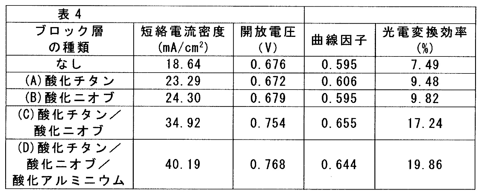
本結果から、酸化チタン、酸化ニオブをそれぞれブロック層として使用した際に、変換効率の向上が認められた。またブロック層を2種類以上のものにて構成させることにより、光電変換特性が2倍以上の飛躍的な向上が認められた。
(e)有利な効果のまとめ
本発明の色素増感型太陽電池は、特異なブロック層を有する。そのブロック層は、光電極及び光電極基板界面で、電解液層への電子の漏出を防いだり、電子と色素増感剤との再結合を防いだりすることができる。
本発明の色素増感型太陽電池は、特異なブロック層を有する。そのブロック層は、光電極及び光電極基板界面で、電解液層への電子の漏出を防いだり、電子と色素増感剤との再結合を防いだりすることができる。
その結果、色素から発生した励起電子は、色素が吸着されている多孔質酸化チタン層を通じて光電極基板に移動する過程において、酸化状態である色素と再結合せず、電解液に接した光電極基板の表面から電解液側に逆電子移動を起こすことが無い。
本発明の色素増感型太陽電池は、その特定のブロック層が設けられていることから、高い光電変換効率を実現する。
(i)ブロック層のチタン材料上に酸化アルミニウム層が形成されていること
本発明の色素増感型太陽電池では、前記実施例2~4で立証される通り、ブロック層のチタン材料上(下層、チタン材料側)に酸化アルミニウム層を設けた場合、高い変換効率を得ることができる。
本発明の色素増感型太陽電池では、前記実施例2~4で立証される通り、ブロック層のチタン材料上(下層、チタン材料側)に酸化アルミニウム層を設けた場合、高い変換効率を得ることができる。
これは、酸化アルミニウムは、ブロック層の材料の中でもバンドギャップ(コンダクションバンドとバレンスバンドとのギャップ)が大きな物質であり、コンダクションバンドのエネルギー値が高い物質であるからである。
色素増感剤の光励起に伴う電子は、コンダクションバンドに移動する。酸化アルミニウムのコンダクションバンドの位置が高いために、この高いコンダクションバンドの壁を越えての電解液側への逆電子移動が難しくなる。
本発明の色素増感型太陽電池では、この様な酸化アルミニウムの特性に基づき、ブロック層のチタン材料上に酸化アルミニウムのブロック層を備えることで、光電変換効率を高めることが可能になる。
(ii)ブロック層が特定の材料であること
本発明の色素増感型太陽電池では、前記説明の通り、ブロック層としてn型半導体を使用することが好ましい。
本発明の色素増感型太陽電池では、前記説明の通り、ブロック層としてn型半導体を使用することが好ましい。
前記実施例2~4に使用した酸化チタン、酸化アルミニウム及び酸化ニオブに加えて、酸化ケイ素、酸化ジルコニウム、チタン酸ストロンチウム及び酸化マグシウムもn型半導体である。
そのため、本発明の色素増感型太陽電池では、酸化チタン、酸化アルミニウム、酸化ニオブに加えて、酸化ケイ素、酸化ジルコニウム、チタン酸ストロンチウム及び酸化マグネシウムも、効果的なブロック層として機能する。
ブロック層として、酸化チタン、酸化アルミニウム及び酸化ニオブを使用し、そのブロック層のチタン材料上(下層)に酸化アルミニウムの層を形成させた実施例を考えれば、ブロック層として、酸化チタンの層、酸化アルミニウムの層、酸化ケイ素の層、酸化ジルコニウムの層、チタン酸ストロンチウムの層、酸化マグネシウムの層及び酸化ニオブの層等の少なくともの2つの層を使う、本発明の色素増感型太陽電池の好ましい態様は、十分にサポートされている。
(iii)光電極のチタン材料上にブロック層を設けること
本発明の色素増感型太陽電池では、光電極基板がチタン材料で形成され、更にブロック層が設けられている。
本発明の色素増感型太陽電池では、光電極基板がチタン材料で形成され、更にブロック層が設けられている。
このブロック層は、光電極及び光電極基板(チタン材料)界面で、電解液層への電子の漏出を防いだり、電子と色素増感剤との再結合を防いだりする。
本発明の色素増感型太陽電池では、このブロック層により、色素から発生した励起電子は、色素が吸着されている多孔質酸化チタン層を通じて、光電極基板に移動する過程において、酸化状態である色素と再結合せず、電解液に接した光電極基板の表面から電解液側に逆電子移動を起こすことが無い。
本発明の色素増感型太陽電池では、光電極基板(チタン材料)上に特定のブロック層を設けることで、光電変換効率が向上する。
(iv)効果が実施例で立証されていること
本発明の色素増感型太陽電池により奏される効果は明細書の実施例で十分に立証されている(実施例2~4等)。
本発明の色素増感型太陽電池により奏される効果は明細書の実施例で十分に立証されている(実施例2~4等)。
本発明の色素増感型太陽電池では、チタン材料上(下層、チタン材料側)に酸化アルミニウム、その上層に酸化チタンにて構成されたブロック層(実施例2及び3の2層構造)や、チタン材料上に酸化アルミニウム、中間層に酸化ニオブ、その上層に酸化チタンのブロック層(実施例4の3層構造)が形成されることで、光電変換特性である短絡電流密度や開放電圧、曲線因子が改善され、光電変換効率の大幅な向上が認められる。
実施例から、ブロック層を2種類以上のものにて構成させることにより、光電変換特性の飛躍的な向上が認められる。
本発明の色素増感型太陽電池が奏する効果は、チタン材料で形成される光電極基板上に特異なブロック層が設けられるという構成要素の結合によりもたらされ、つまり発明特定事項の各々が互いに機能的又は作用的に関連して得られる効果である。この効果は、従来技術に見つからず、有利な効果と言える。
1 光電極(チタン基板、チタン材料)
2 陽極酸化材(アナターゼ型酸化チタンの皮膜)
3 ブロック層(緻密な層)
4 色素増感剤を含有する酸化チタン層(多孔質)
5 電解液(電解質層)
6 スペーサー、封止材
7 白金蒸着膜(電気化学的還元触媒層)
8 FTO膜(透明導電膜)
9 対極(ガラス又はフィルム)
2 陽極酸化材(アナターゼ型酸化チタンの皮膜)
3 ブロック層(緻密な層)
4 色素増感剤を含有する酸化チタン層(多孔質)
5 電解液(電解質層)
6 スペーサー、封止材
7 白金蒸着膜(電気化学的還元触媒層)
8 FTO膜(透明導電膜)
9 対極(ガラス又はフィルム)
Claims (8)
- 光電極と対極とが電解質層を介して対向配置された色素増感太陽電池であって、
(1)光電極が、チタン材料上にブロック層が設けられ、更に該ブロック層上に色素増感剤を含有する多孔質酸化チタン層が形成されたものであり、
該ブロック層は、酸化チタンの層、酸化アルミニウムの層、酸化ケイ素の層、酸化ジルコニウムの層、チタン酸ストロンチウムの層、酸化マグネシウムの層及び酸化ニオブの層からなる群から選ばれる少なくともの2つの層で構成され、必ず、該ブロック層のチタン材料上に酸化アルミニウムの層が形成されており、
(2)対極が、透明導電性ガラス又は透明導電性フィルム上に、電気化学的還元触媒層がコーティングされていることを特徴とする、色素増感太陽電池。 - 前記チタン材料が、金属チタン、チタン合金、表面処理した金属チタン及び表面処理したチタン合金からなる群から選ばれる材料であることを特徴とする、請求項1に記載の色素増感太陽電池。
- 前記電気化学的還元触媒層が、白金触媒層であることを特徴とする、請求項1又は2に記載の色素増感太陽電池。
- 前記ブロック層が、酸化チタンの層、酸化アルミニウムの層及び酸化ニオブの層からなる群から選ばれる少なくともの2つの層で構成されること特徴とする、請求項1~3のいずれかに記載の色素増感太陽電池。
- 請求項1~4のいずれかに記載の色素増感太陽電池の製造方法であって、
前記光電極のチタン材料が、以下の表面処理方法により製造される製造方法:
(1)金属チタン材料又はチタン材料の表面にチタン窒化物を形成する工程、及び
(2)工程(1)で得られた、表面にチタン窒化物を形成された金属チタン材料又はチタン合金材料を、チタンに対してエッチング作用を有する電解液を用いて、火花放電発生電圧以上にて陽極酸化を行い、アナターゼ型酸化チタンの皮膜を形成する工程。 - 請求項1~4のいずれかに記載の色素増感太陽電池の製造方法であって、
前記光電極のチタン材料が、以下の表面処理方法により製造される製造方法:
(1)金属チタン材料又はチタン材料の表面にチタン窒化物を形成する工程、
(2)工程(1)で得られた、表面にチタン窒化物を形成された金属チタン材料又はチタン合金材料を、チタンに対してエッチング作用を有しない電解液を用いて、陽極酸化を行う工程、及び
(3)工程(2)で得られた、陽極酸化処理を施した金属チタン材料又はチタン合金材料を、酸化性雰囲気中で加熱処理を行い、アナターゼ型酸化チタン皮膜を形成する工程。 - 前記チタン窒化物を形成する工程が、PVD処理、CVD処理、溶射処理、アンモニアガス雰囲気下での加熱処理及び窒素ガス雰囲気下での加熱処理よりなる群から選択された1種の処理方法により行うものであること特徴とする、請求項5又は6に記載の製造方法。
- 前記窒素ガス雰囲気下での加熱処理が、酸素トラップ剤の存在下で実施するものであること特徴とする、請求項7に記載の製造方法。
Priority Applications (4)
| Application Number | Priority Date | Filing Date | Title |
|---|---|---|---|
| CN201780001673.0A CN107710363A (zh) | 2016-05-12 | 2017-04-28 | 具有高转换效率的色素敏化太阳能电池 |
| US15/574,001 US20190066932A1 (en) | 2016-05-12 | 2017-04-28 | Dye sensitized solar cell having high photoelectric conversion efficiency |
| EP17796009.3A EP3288052A4 (en) | 2016-05-12 | 2017-04-28 | SOLAR CELL SENSITIZED BY DYE WITH HIGH CONVERSION EFFICIENCY |
| KR1020177032121A KR20190008063A (ko) | 2016-05-12 | 2017-04-28 | 고변환 효율을 가지는 색소 증감 태양 전지 |
Applications Claiming Priority (2)
| Application Number | Priority Date | Filing Date | Title |
|---|---|---|---|
| JP2016096200A JP6058190B1 (ja) | 2016-05-12 | 2016-05-12 | 高変換効率を有する色素増感太陽電池 |
| JP2016-096200 | 2016-05-12 |
Publications (1)
| Publication Number | Publication Date |
|---|---|
| WO2017195648A1 true WO2017195648A1 (ja) | 2017-11-16 |
Family
ID=57756231
Family Applications (1)
| Application Number | Title | Priority Date | Filing Date |
|---|---|---|---|
| PCT/JP2017/016891 Ceased WO2017195648A1 (ja) | 2016-05-12 | 2017-04-28 | 高変換効率を有する色素増感太陽電池 |
Country Status (7)
| Country | Link |
|---|---|
| US (1) | US20190066932A1 (ja) |
| EP (1) | EP3288052A4 (ja) |
| JP (1) | JP6058190B1 (ja) |
| KR (1) | KR20190008063A (ja) |
| CN (1) | CN107710363A (ja) |
| TW (1) | TW201909437A (ja) |
| WO (1) | WO2017195648A1 (ja) |
Families Citing this family (2)
| Publication number | Priority date | Publication date | Assignee | Title |
|---|---|---|---|---|
| DE112019001222T5 (de) | 2018-03-09 | 2020-11-26 | Schlumberger Technology B.V. | Integrierte Bohrlochkonstruktionssystem-Betriebsvorgänge |
| JP7410117B2 (ja) * | 2018-07-16 | 2024-01-09 | エクセジャー オペレーションズ エービー | 色素増感型太陽電池ユニット、色素増感型太陽電池ユニットを含む光起電力充電器および前記太陽電池ユニットの製造方法 |
Citations (7)
| Publication number | Priority date | Publication date | Assignee | Title |
|---|---|---|---|---|
| JP2008077924A (ja) | 2006-09-20 | 2008-04-03 | Nippon Sheet Glass Co Ltd | 光電変換装置 |
| WO2009113342A1 (ja) * | 2008-03-14 | 2009-09-17 | コニカミノルタホールディングス株式会社 | 色素増感型太陽電池 |
| WO2010090226A1 (ja) * | 2009-02-03 | 2010-08-12 | 株式会社昭和 | 色素増感型太陽電池 |
| JP2012199228A (ja) * | 2011-03-09 | 2012-10-18 | Osaka Gas Co Ltd | 全固体光増感太陽電池 |
| WO2014064965A1 (ja) * | 2012-10-23 | 2014-05-01 | 学校法人東京理科大学 | 色素増感太陽電池用光電極および色素増感太陽電池 |
| JP2014220180A (ja) * | 2013-05-10 | 2014-11-20 | 株式会社昭和 | 高耐久性、高変換効率を有する色素増感型太陽電池 |
| WO2016182025A1 (ja) * | 2015-05-14 | 2016-11-17 | 株式会社昭和 | 対極に集電極を設けた色素増感型太陽電池 |
Family Cites Families (6)
| Publication number | Priority date | Publication date | Assignee | Title |
|---|---|---|---|---|
| NL1009431C2 (nl) * | 1998-06-18 | 1999-12-27 | Stichting Energie | Omgekeerde kleurstof-gesensibiliseerde foto-voltaïsche cel. |
| CN101238244B (zh) * | 2005-01-24 | 2011-03-30 | 株式会社昭和 | 采用阳极电解氧化处理的结晶性氧化钛被膜的制造方法 |
| CN101193909A (zh) * | 2005-05-23 | 2008-06-04 | 创新生命化学日本株式会社 | 具有光敏化作用的化合物、光电极及光敏化型太阳电池 |
| US20140216553A1 (en) * | 2013-02-04 | 2014-08-07 | Sean Vail | Dye-Sensitized Solar Cell via Co-Sensitization with Cooperative Dyes |
| JP5689190B1 (ja) * | 2014-01-27 | 2015-03-25 | 株式会社昭和 | 集光装置を設けた色素増感型太陽電池 |
| US20170243698A1 (en) * | 2016-02-22 | 2017-08-24 | Ricoh Company, Ltd. | Photoelectric conversion element |
-
2016
- 2016-05-12 JP JP2016096200A patent/JP6058190B1/ja not_active Expired - Fee Related
-
2017
- 2017-04-28 CN CN201780001673.0A patent/CN107710363A/zh active Pending
- 2017-04-28 WO PCT/JP2017/016891 patent/WO2017195648A1/ja not_active Ceased
- 2017-04-28 EP EP17796009.3A patent/EP3288052A4/en not_active Withdrawn
- 2017-04-28 KR KR1020177032121A patent/KR20190008063A/ko not_active Ceased
- 2017-04-28 US US15/574,001 patent/US20190066932A1/en not_active Abandoned
- 2017-05-04 TW TW106114847A patent/TW201909437A/zh unknown
Patent Citations (7)
| Publication number | Priority date | Publication date | Assignee | Title |
|---|---|---|---|---|
| JP2008077924A (ja) | 2006-09-20 | 2008-04-03 | Nippon Sheet Glass Co Ltd | 光電変換装置 |
| WO2009113342A1 (ja) * | 2008-03-14 | 2009-09-17 | コニカミノルタホールディングス株式会社 | 色素増感型太陽電池 |
| WO2010090226A1 (ja) * | 2009-02-03 | 2010-08-12 | 株式会社昭和 | 色素増感型太陽電池 |
| JP2012199228A (ja) * | 2011-03-09 | 2012-10-18 | Osaka Gas Co Ltd | 全固体光増感太陽電池 |
| WO2014064965A1 (ja) * | 2012-10-23 | 2014-05-01 | 学校法人東京理科大学 | 色素増感太陽電池用光電極および色素増感太陽電池 |
| JP2014220180A (ja) * | 2013-05-10 | 2014-11-20 | 株式会社昭和 | 高耐久性、高変換効率を有する色素増感型太陽電池 |
| WO2016182025A1 (ja) * | 2015-05-14 | 2016-11-17 | 株式会社昭和 | 対極に集電極を設けた色素増感型太陽電池 |
Non-Patent Citations (1)
| Title |
|---|
| See also references of EP3288052A4 |
Also Published As
| Publication number | Publication date |
|---|---|
| KR20190008063A (ko) | 2019-01-23 |
| EP3288052A4 (en) | 2019-05-01 |
| JP6058190B1 (ja) | 2017-01-11 |
| EP3288052A1 (en) | 2018-02-28 |
| JP2017204585A (ja) | 2017-11-16 |
| TW201909437A (zh) | 2019-03-01 |
| CN107710363A (zh) | 2018-02-16 |
| US20190066932A1 (en) | 2019-02-28 |
Similar Documents
| Publication | Publication Date | Title |
|---|---|---|
| KR100947371B1 (ko) | 다파장 흡수 나노 구조 염료감응 태양전지 및 그 제조방법 | |
| JP5840170B2 (ja) | 高耐久性、高変換効率を有する色素増感型太陽電池 | |
| EP2963154B1 (en) | Method for producing surface-treated metal titanium material or titanium alloy material | |
| JP5689190B1 (ja) | 集光装置を設けた色素増感型太陽電池 | |
| Mehmood et al. | Spray coated PbS nano-crystals as an effective counter-electrode material for platinum free Dye-Sensitized Solar Cells (DSSCs) | |
| JP6161860B2 (ja) | 対極に集電極を設けた色素増感型太陽電池 | |
| JP6058190B1 (ja) | 高変換効率を有する色素増感太陽電池 | |
| JP6104446B1 (ja) | 色素増感型太陽電池モジュール | |
| KR100930922B1 (ko) | 염료감응태양전지 및 그 제조방법 | |
| KR20090096067A (ko) | 비드밀 분산기를 이용한 금속산화물 나노입자의 분산방법및 상기 금속산화물 나노입자를 포함하는 염료감응태양전지 | |
| JP5689202B1 (ja) | 集光装置を設けた色素増感型太陽電池 | |
| JP2015142131A (ja) | 集光装置を設けた色素増感型太陽電池 | |
| WO2015037714A1 (ja) | 複合膜の製造方法、複合膜、光電極および色素増感太陽電池 | |
| JP2021125509A (ja) | 高い発電量が得られる色素増感型太陽電池 |
Legal Events
| Date | Code | Title | Description |
|---|---|---|---|
| ENP | Entry into the national phase |
Ref document number: 20177032121 Country of ref document: KR Kind code of ref document: A |
|
| NENP | Non-entry into the national phase |
Ref country code: DE |