WO2017195810A1 - Élément de déphasage, procédé de fabrication d'un élément de déphasage et élément optique - Google Patents
Élément de déphasage, procédé de fabrication d'un élément de déphasage et élément optique Download PDFInfo
- Publication number
- WO2017195810A1 WO2017195810A1 PCT/JP2017/017644 JP2017017644W WO2017195810A1 WO 2017195810 A1 WO2017195810 A1 WO 2017195810A1 JP 2017017644 W JP2017017644 W JP 2017017644W WO 2017195810 A1 WO2017195810 A1 WO 2017195810A1
- Authority
- WO
- WIPO (PCT)
- Prior art keywords
- phase difference
- difference element
- electromagnetic wave
- metal
- wavelength
- Prior art date
- Legal status (The legal status is an assumption and is not a legal conclusion. Google has not performed a legal analysis and makes no representation as to the accuracy of the status listed.)
- Ceased
Links
Images








Classifications
-
- G—PHYSICS
- G02—OPTICS
- G02B—OPTICAL ELEMENTS, SYSTEMS OR APPARATUS
- G02B5/00—Optical elements other than lenses
- G02B5/30—Polarising elements
-
- G—PHYSICS
- G02—OPTICS
- G02F—OPTICAL DEVICES OR ARRANGEMENTS FOR THE CONTROL OF LIGHT BY MODIFICATION OF THE OPTICAL PROPERTIES OF THE MEDIA OF THE ELEMENTS INVOLVED THEREIN; NON-LINEAR OPTICS; FREQUENCY-CHANGING OF LIGHT; OPTICAL LOGIC ELEMENTS; OPTICAL ANALOGUE/DIGITAL CONVERTERS
- G02F1/00—Devices or arrangements for the control of the intensity, colour, phase, polarisation or direction of light arriving from an independent light source, e.g. switching, gating or modulating; Non-linear optics
- G02F1/01—Devices or arrangements for the control of the intensity, colour, phase, polarisation or direction of light arriving from an independent light source, e.g. switching, gating or modulating; Non-linear optics for the control of the intensity, phase, polarisation or colour
- G02F1/13—Devices or arrangements for the control of the intensity, colour, phase, polarisation or direction of light arriving from an independent light source, e.g. switching, gating or modulating; Non-linear optics for the control of the intensity, phase, polarisation or colour based on liquid crystals, e.g. single liquid crystal display cells
- G02F1/133—Constructional arrangements; Operation of liquid crystal cells; Circuit arrangements
- G02F1/1333—Constructional arrangements; Manufacturing methods
- G02F1/1335—Structural association of cells with optical devices, e.g. polarisers or reflectors
-
- G—PHYSICS
- G02—OPTICS
- G02F—OPTICAL DEVICES OR ARRANGEMENTS FOR THE CONTROL OF LIGHT BY MODIFICATION OF THE OPTICAL PROPERTIES OF THE MEDIA OF THE ELEMENTS INVOLVED THEREIN; NON-LINEAR OPTICS; FREQUENCY-CHANGING OF LIGHT; OPTICAL LOGIC ELEMENTS; OPTICAL ANALOGUE/DIGITAL CONVERTERS
- G02F1/00—Devices or arrangements for the control of the intensity, colour, phase, polarisation or direction of light arriving from an independent light source, e.g. switching, gating or modulating; Non-linear optics
- G02F1/01—Devices or arrangements for the control of the intensity, colour, phase, polarisation or direction of light arriving from an independent light source, e.g. switching, gating or modulating; Non-linear optics for the control of the intensity, phase, polarisation or colour
- G02F1/13—Devices or arrangements for the control of the intensity, colour, phase, polarisation or direction of light arriving from an independent light source, e.g. switching, gating or modulating; Non-linear optics for the control of the intensity, phase, polarisation or colour based on liquid crystals, e.g. single liquid crystal display cells
- G02F1/133—Constructional arrangements; Operation of liquid crystal cells; Circuit arrangements
- G02F1/1333—Constructional arrangements; Manufacturing methods
- G02F1/1335—Structural association of cells with optical devices, e.g. polarisers or reflectors
- G02F1/13363—Birefringent elements, e.g. for optical compensation
Definitions
- the present invention relates to a retardation element, a retardation element manufacturing method, and an optical member using the retardation element.
- the conventional phase difference element uses the difference in propagation speed or absorption characteristics depending on the material, and creates a phase difference between two orthogonal polarization components, changing the polarization state from linearly polarized light to circularly polarized light.
- This is an optical element.
- Such an element is used, for example, for switching on / off a pixel of an image projection apparatus such as a liquid crystal panel, an organic EL display, or a liquid crystal projector. It is also widely used in various optical instruments and measuring instruments such as optical measurement techniques such as ellipsometry (polarization analysis), laser interferometers, and optical shutters.
- phase difference element one in which a plurality of openings are periodically arranged in a metal film has been disclosed (for example, Patent Document 1).
- optical member which combined the said phase difference element with the polarizing plate like a wire grid is disclosed (for example, patent document 2).
- the conventional retardation plate has a triangular or rectangular opening, and its processing is difficult.
- an object of the present invention is to provide a phase difference element, a phase difference element manufacturing method, and an optical member using the phase difference element that have high ellipticity and transmittance and are easy to process.
- the retardation element of the present invention is for controlling the optical characteristics of an incident electromagnetic wave, and a linear metal structure having a width smaller than the wavelength of the electromagnetic wave is arranged in parallel. It is characterized by comprising a periodically arranged metal part and a dielectric part made of a dielectric material that can transmit the electromagnetic wave and supporting the metal structure.
- the space between the metal structures may be filled with the dielectric.
- the metal part may be included in the dielectric.
- the metal structure may have a convex cross section with a small width on the incident direction side of the electromagnetic wave.
- the ellipticity of electromagnetic waves when transmitting linearly polarized electromagnetic waves is 70% or more. Further, when the wavelength of the electromagnetic wave is ⁇ , it is preferable that the pitch of the metal structure is formed to be ⁇ or less.
- the pitch of the metal structures is formed to be 0.35 ⁇ or more.
- the optical member of the present invention includes a reflective polarizer that polarizes incident electromagnetic waves and the retardation element of the present application, and the metal structure 1 of the retardation element passes through the polarizing element. It is characterized in that it is periodically arranged in a direction of 40 to 50 degrees with respect to the polarization direction.
- Another optical member of the present invention includes a reflective polarizer that polarizes incident electromagnetic waves, the retardation element of the present application, and a light emitting unit that is disposed between the polarizing element and the retardation element and that emits light. And a mirror that reflects the electromagnetic wave that has passed through the phase difference element to the phase difference element side, and the metal structure of the phase difference element has a polarization direction of the electromagnetic wave that has passed through the polarizing element. It is characterized by being periodically arranged in a direction of 40 to 50 degrees.
- the mirror is disposed apart from the metal portion of the retardation element.
- the phase difference element manufacturing method of the present invention is for manufacturing a phase difference element for controlling optical characteristics of incident electromagnetic waves, and the electromagnetic wave is applied to a dielectric made of a resin capable of transmitting the electromagnetic waves.
- a covering step of covering the exposed portion of the metal with a dielectric material that can transmit the electromagnetic wave it is preferable to have a covering step of covering the exposed portion of the metal with a dielectric material that can transmit the electromagnetic wave.
- the retardation element of the present invention has an effect of having a high ellipticity and transmittance while having a simple structure.
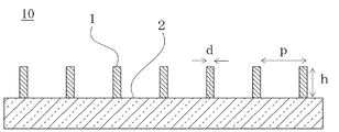
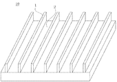
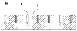
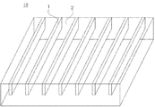
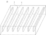
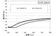
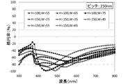
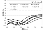
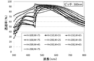
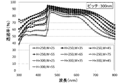
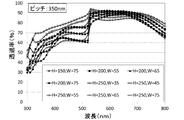
- phase difference element of this invention It is a schematic sectional drawing which shows the phase difference element of this invention. It is a schematic perspective view which shows the phase difference element of this invention. It is a schematic sectional drawing which shows another phase difference element of this invention. It is a schematic perspective view which shows another phase difference element of this invention. It is a schematic sectional drawing which shows another phase difference element of this invention. It is a schematic perspective view which shows another phase difference element of this invention. It is a schematic perspective view which shows another phase difference element of this invention. It is a graph which shows the relationship between the wavelength of an incident wave, and ellipticity in the phase difference element (pitch of 150 nm) of this invention. It is a graph which shows the relationship between the wavelength of an incident wave, and an ellipticity in the phase difference element (200 nm pitch) of this invention.
- the phase difference element 10 of the present invention is for controlling the optical characteristics of an incident electromagnetic wave, and includes a metal part composed of a plurality of metal structures 1 and a dielectric part 2. And is composed mainly of.
- the metal part has a line and space shape in which a plurality of linear metal structures 1 are arranged in parallel.
- the metal structure 1 is formed to have a width smaller than the wavelength of the electromagnetic wave.
- the cross section of the metal structure 1 shows the ellipticity of the transmitted wave when an electromagnetic wave having a predetermined wavelength which is linearly polarized light is incident at an angle of 45 degrees with respect to the linear direction of the metal structure 1. Any value can be used as long as the absolute value of becomes 70% or more.
- a cross section having a quadrangle, a triangle, or a trapezoid can be used.
- Examples of the metal include silver, gold, aluminum, nickel, and copper. Of course, it is not limited to these.
- the electromagnetic wave passes between the metal structures 1 of the metal part formed in this way, so that a phase difference can be given to the electromagnetic wave.
- the pitch P between the metal structures 1 is the ellipticity of the transmitted wave when electromagnetic waves that are linearly polarized light are incident at an angle of 45 degrees with respect to the linear direction of the metal structure 1. Any value can be used as long as the absolute value is 70% or more.
- the ellipticity means the ratio b / a of the major axis length a and the minor axis length b of the ellipse when the locus of the electromagnetic wave is projected onto a plane perpendicular to the traveling direction of the electromagnetic wave.
- the absolute value of this ellipticity is 70% or more, the transmitted wave can be regarded as circularly polarized light within 3 dB.
- the width and height of the metal structure 1 is also set so that the electromagnetic wave, which is linearly polarized light, has an ellipticity of the transmitted wave when the polarization direction is incident at an angle of 45 degrees with respect to the linear direction of the metal structure 1. Any value can be used as long as the absolute value is 70% or more.
- the metal structure may have a convex cross section with a small width on the incident direction side of the electromagnetic wave. Note that the transmittance of electromagnetic waves can be adjusted by the width and height of the metal structure 1.
- the dielectric portion 2 is made of a dielectric material that can transmit electromagnetic waves, and is for supporting the metal structure 1. Any dielectric material may be used as long as it can transmit a desired electromagnetic wave.
- a transparent resin that can be processed by a photolithography technique, a nanoimprint technique, or the like may be used. It is also possible to use a transparent inorganic compound such as silicon (Si) or silicon dioxide (SiO 2 ).
- the dielectric part 2 may be filled with the dielectric material between the metal structures 1, or the metal part may be completely enclosed in the dielectric part 2. Thereby, intensity
- phase difference element 10 of the present invention will be described using simulation.
- a software DiffractMOD manufactured by Synopsys, Inc. was used.
- a line-and-space shape in which a plurality of metal structures 1 each having a straight metal part and a rectangular cross section are arranged in parallel is used.
- the metal is aluminum, and the periphery of the metal structure 1 is a dielectric having a refractive index of 1.5.
- the incident electromagnetic wave (incident wave) was linearly polarized light, and the polarization direction was an angle of 45 degrees with respect to the linear direction of the metal structure 1.
- the incident electromagnetic waves were calculated such that the wavelengths differed by 10 nm from 300 to 800 nm.
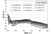
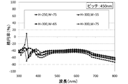
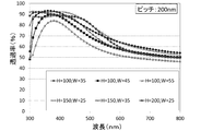
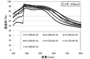
- FIG. 7 to FIG. 16 show the relationship between the wavelength of the incident wave and the ellipticity of the transmitted wave when the pitch P, height H, and width W of the metal structure 1 are changed as shown in Table 1.
- the results of wave transmittance are shown in FIGS.
- the phase difference element 10 of the present application has an absolute value of ellipticity of 70% or more in a wide wavelength band.
- permeability is also very large.
- the pitch P of the metal structure 1 is 350 nm
- the height H is 300 nm
- the width W is 45 nm
- the incident wave has a wavelength ⁇ of 570 to 790 nm.
- the absolute value of the ellipticity of the wave is 70% or more.
- the transmittance in this range is 78.4% or more, and the maximum is 90.7%.
- the wavelength of the incident electromagnetic wave which is linearly polarized light
- ⁇ at least 0 for the absolute value of the ellipticity of the transmitted wave to be 70% or more and the transmittance to be more than 60%. .35 ⁇ ⁇ P ⁇ ⁇ is preferable.
- the method of manufacturing the retardation element 10 of the present invention includes a groove forming step of forming a plurality of linear grooves having a width smaller than the wavelength of an electromagnetic wave at a predetermined interval in a dielectric made of a resin that can transmit electromagnetic waves, and a metal in the groove And a metal part forming step for filling the metal.
- the groove forming step may be any process as long as the groove for forming the metal part can be formed.
- the groove may be formed in the dielectric by a conventionally known photolithography technique, nanoimprint technique, or the like.
- the metal part forming process may be any process as long as the groove created in the groove forming process can be filled with metal.
- the metal formed other than the groove is polished or the like. Can be removed. As a result, a line-and-space-shaped metal portion in which a plurality of linear metal structures 1 are arranged in parallel can be formed.
- a coating step of covering with a dielectric that can transmit electromagnetic waves in the portion where the metal is exposed may be provided. Any method may be used for coating with a dielectric, but the surface of the metal structure 1 may be covered with a dielectric using a method such as coating, vapor deposition, laser ablation, or CVD.
- the optical member 100 of the present invention is mainly composed of a polarizer 20 and a retardation element 10 of the present invention.
- the polarizer 20 allows only incident electromagnetic waves that are polarized or polarized in a specific direction to pass through.
- the polarizer 20 includes a reflective type that reflects a component of an electromagnetic wave that has not passed, and an absorption type that absorbs an electromagnetic wave that has not passed.
- a conventionally known one such as a wire grid may be used.
- phase difference element 10 the phase difference element 10 of the present invention described above may be used.
- the phase difference element 10 is arranged so that the linear direction of the metal structure 1 is 40 to 50 degrees, preferably 45 degrees with respect to the polarization direction of the electromagnetic wave that has passed through the polarizer 20. Thereby, the linearly polarized light that has passed through the polarizer 20 can be changed to a circularly polarized or elliptically polarized state.
- various incident electromagnetic waves can be converted into linearly polarized light by a polarizer, and the linearly polarized light can be converted into circularly polarized light by a phase difference element.
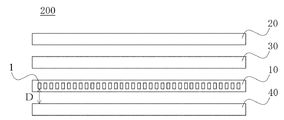
- the optical member 200 of the present invention is mainly composed of a polarizer 20, the phase difference element 10 of the present invention, a light emitting unit 30, and a mirror 40. As shown in FIG.
- the polarizer 20 allows only incident electromagnetic waves that are polarized or polarized in a specific direction to pass through.
- the polarizer 20 is a reflective type that reflects the component of the electromagnetic wave that has not passed.
- phase difference element 10 the phase difference element 10 of the present invention described above may be used.
- the phase difference element 10 is arranged so that the linear direction of the metal structure 1 is 40 to 50 degrees, preferably 45 degrees with respect to the polarization direction of the electromagnetic wave that has passed through the polarizer 20. Thereby, the linearly polarized light that has passed through the polarizer 20 can be changed to a circularly polarized or elliptically polarized state.
- the light emitting unit 30 is disposed between the polarizing element and the phase difference element 10 and irradiates desired light (electromagnetic wave).
- a conventionally known light emitting unit 30 may be used.
- the light emitting unit 30 such as a display or a laser interferometer is applicable.
- the light emitting unit 30 in FIG. 28 corresponds to a waveguide plate of a display.
- the mirror 40 is for reflecting the electromagnetic wave that has passed through the phase difference element 10 to the phase difference element 10 side.
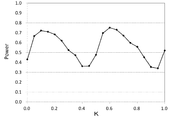
- the wavelength ⁇ of the electromagnetic wave has the relationship of the following formula (1).
- K is a coefficient.
- D K ⁇ ⁇ / 1.5 (1)
- the extraction efficiency of light that can be extracted from the optical member 200 out of the light output from the light emitting unit 30 has the relationship shown in FIG.
- the electromagnetic wave incident on the polarizer 20 from the light emitting unit 30 passes only the P-polarized light having a specific direction component through the polarizer 20 and is S-polarized light having a component perpendicular to the P-polarized light.
- the reflected S-polarized light passes through the phase difference element 10
- a phase difference is generated and converted to circularly polarized light (or elliptically polarized light).
- the circularly polarized light or elliptically polarized light
- this electromagnetic wave passes through the phase difference element 10 again, it is converted back to linearly polarized light.
- the electromagnetic wave is converted into an electromagnetic wave that is nearly perpendicular to the incident S-polarized light.
- the angle is determined according to the ellipticity, and when the absolute value of the ellipticity is 1, P-polarized light is obtained.
- most of the electromagnetic waves irradiated from the light emitting unit 30 can pass through the polarizer 20, and the polarization extraction efficiency can be improved.
- the polarizer 20, the phase difference element 10, the light emitting unit 30, and the mirror 40 may be anything that can transmit electromagnetic waves emitted from the light emitting unit, and may be in contact with each other. good. However, as described above, it is preferable to dispose the mirror 40 at least apart from the metal portion of the phase difference element 10.
- Metal structure 2 Dielectric part 10 Phase difference element 20 Polarizer 30 Light emitter 40 mirror
Landscapes
- Physics & Mathematics (AREA)
- Nonlinear Science (AREA)
- General Physics & Mathematics (AREA)
- Optics & Photonics (AREA)
- Mathematical Physics (AREA)
- Chemical & Material Sciences (AREA)
- Crystallography & Structural Chemistry (AREA)
- Polarising Elements (AREA)
Abstract
Le but de la présente invention est de proposer : un élément de déphasage qui présente une ellipticité élevée et une transmittance élevée et qui est facilement usiné ; un procédé de fabrication d'un élément de déphasage ; et un élément optique qui utilise l'élément de déphasage. Un élément de déphasage (10) servant à contrôler les caractéristiques optiques d'une onde électromagnétique incidente est doté : d'une partie métallique dans laquelle des structures métalliques linéaires (1) présentant des largeurs inférieures à la longueur d'onde de l'onde électromagnétique sont périodiquement disposées en parallèle ; et d'une partie diélectrique (2) qui soutient les structures métalliques (1) et qui comprend un corps diélectrique à travers lequel peuvent passer des ondes électromagnétiques.
Priority Applications (1)
| Application Number | Priority Date | Filing Date | Title |
|---|---|---|---|
| JP2018517049A JPWO2017195810A1 (ja) | 2016-05-11 | 2017-05-10 | 位相差素子、位相差素子製造方法および光学部材 |
Applications Claiming Priority (2)
| Application Number | Priority Date | Filing Date | Title |
|---|---|---|---|
| JP2016-095351 | 2016-05-11 | ||
| JP2016095351 | 2016-05-11 |
Publications (1)
| Publication Number | Publication Date |
|---|---|
| WO2017195810A1 true WO2017195810A1 (fr) | 2017-11-16 |
Family
ID=60267859
Family Applications (1)
| Application Number | Title | Priority Date | Filing Date |
|---|---|---|---|
| PCT/JP2017/017644 Ceased WO2017195810A1 (fr) | 2016-05-11 | 2017-05-10 | Élément de déphasage, procédé de fabrication d'un élément de déphasage et élément optique |
Country Status (2)
| Country | Link |
|---|---|
| JP (1) | JPWO2017195810A1 (fr) |
| WO (1) | WO2017195810A1 (fr) |
Citations (5)
| Publication number | Priority date | Publication date | Assignee | Title |
|---|---|---|---|---|
| JP2007532977A (ja) * | 2004-04-15 | 2007-11-15 | ナノオプト コーポレーション | 光学膜およびその製造方法 |
| JP2008180875A (ja) * | 2007-01-24 | 2008-08-07 | Hitachi Displays Ltd | 偏光子及びそれを用いた液晶表示装置 |
| JP2010277016A (ja) * | 2009-06-01 | 2010-12-09 | Ricoh Co Ltd | 光学フィルタおよび画像撮影装置 |
| US20150116824A1 (en) * | 2013-10-24 | 2015-04-30 | Moxtek, Inc. | Polarizer with wire pair over rib |
| JP2016051162A (ja) * | 2014-08-29 | 2016-04-11 | 学校法人法政大学 | 金属膜に周期的に非対称開口を配設した位相差板 |
-
2017
- 2017-05-10 WO PCT/JP2017/017644 patent/WO2017195810A1/fr not_active Ceased
- 2017-05-10 JP JP2018517049A patent/JPWO2017195810A1/ja active Pending
Patent Citations (5)
| Publication number | Priority date | Publication date | Assignee | Title |
|---|---|---|---|---|
| JP2007532977A (ja) * | 2004-04-15 | 2007-11-15 | ナノオプト コーポレーション | 光学膜およびその製造方法 |
| JP2008180875A (ja) * | 2007-01-24 | 2008-08-07 | Hitachi Displays Ltd | 偏光子及びそれを用いた液晶表示装置 |
| JP2010277016A (ja) * | 2009-06-01 | 2010-12-09 | Ricoh Co Ltd | 光学フィルタおよび画像撮影装置 |
| US20150116824A1 (en) * | 2013-10-24 | 2015-04-30 | Moxtek, Inc. | Polarizer with wire pair over rib |
| JP2016051162A (ja) * | 2014-08-29 | 2016-04-11 | 学校法人法政大学 | 金属膜に周期的に非対称開口を配設した位相差板 |
Also Published As
| Publication number | Publication date |
|---|---|
| JPWO2017195810A1 (ja) | 2019-03-07 |
Similar Documents
| Publication | Publication Date | Title |
|---|---|---|
| JP7187745B2 (ja) | 両側において高い反射率を有するワイヤグリッド偏光子 | |
| JP2006517307A (ja) | 汎用広帯域偏光器、それを含むデバイスおよびその製造方法 | |
| JP2005172844A (ja) | ワイヤグリッド偏光子 | |
| CN107179576B (zh) | 一种可见光波段的渐变相位金属光栅 | |
| JP2012181420A (ja) | 偏光素子 | |
| JP5936727B2 (ja) | 偏光素子 | |
| JP2016534418A (ja) | ワイヤ間距離が可変な偏光子 | |
| TWI625559B (zh) | 偏光片、偏光片用基板及光配向裝置 | |
| JP5206029B2 (ja) | 液晶表示装置 | |
| JP5359128B2 (ja) | 偏光素子及びその製造方法 | |
| US10809426B2 (en) | Wideband resonant reflectors with zero-contrast gratings | |
| CN107209313A (zh) | 高对比度逆偏振器 | |
| JP6047051B2 (ja) | 光学素子および光学装置 | |
| CN111596402B (zh) | 一种基于超构表面的多偏振态产生器 | |
| JP6428171B2 (ja) | 偏光子、偏光子用基板および光配向装置 | |
| CN105814464B (zh) | 偏振系统 | |
| JP2015125252A (ja) | 偏光板およびそれを用いた液晶プロジェクタ | |
| JPWO2017195810A1 (ja) | 位相差素子、位相差素子製造方法および光学部材 | |
| WO2015072482A1 (fr) | Polariseur, substrat de polariseur et dispositif d'alignement optique | |
| WO2015008648A1 (fr) | Lame de phase | |
| KR100919578B1 (ko) | 노광 장치 및 이를 이용한 반도체 소자의 형성 방법 | |
| Ma et al. | Wideband polarizer in the middle IR wavelength region based on guided mode resonance effect | |
| JP4664866B2 (ja) | 光処理素子 | |
| JPH03157621A (ja) | 偏光光源装置 | |
| JP2017026824A (ja) | 偏光解消素子及びその製造方法、並びにそれを用いた光学機器及び液晶表示装置 |
Legal Events
| Date | Code | Title | Description |
|---|---|---|---|
| ENP | Entry into the national phase |
Ref document number: 2018517049 Country of ref document: JP Kind code of ref document: A |
|
| NENP | Non-entry into the national phase |
Ref country code: DE |
|
| 121 | Ep: the epo has been informed by wipo that ep was designated in this application |
Ref document number: 17796170 Country of ref document: EP Kind code of ref document: A1 |
|
| 122 | Ep: pct application non-entry in european phase |
Ref document number: 17796170 Country of ref document: EP Kind code of ref document: A1 |