WO2017199594A1 - Structure de câblage et dispositif électronique - Google Patents
Structure de câblage et dispositif électronique Download PDFInfo
- Publication number
- WO2017199594A1 WO2017199594A1 PCT/JP2017/013298 JP2017013298W WO2017199594A1 WO 2017199594 A1 WO2017199594 A1 WO 2017199594A1 JP 2017013298 W JP2017013298 W JP 2017013298W WO 2017199594 A1 WO2017199594 A1 WO 2017199594A1
- Authority
- WO
- WIPO (PCT)
- Prior art keywords
- porous substrate
- wiring structure
- wiring
- fibrous porous
- layer
- Prior art date
- Legal status (The legal status is an assumption and is not a legal conclusion. Google has not performed a legal analysis and makes no representation as to the accuracy of the status listed.)
- Ceased
Links
Images







Classifications
-
- H—ELECTRICITY
- H05—ELECTRIC TECHNIQUES NOT OTHERWISE PROVIDED FOR
- H05K—PRINTED CIRCUITS; CASINGS OR CONSTRUCTIONAL DETAILS OF ELECTRIC APPARATUS; MANUFACTURE OF ASSEMBLAGES OF ELECTRICAL COMPONENTS
- H05K1/00—Printed circuits
- H05K1/02—Details
- H05K1/03—Use of materials for the substrate
- H05K1/038—Textiles
-
- H—ELECTRICITY
- H05—ELECTRIC TECHNIQUES NOT OTHERWISE PROVIDED FOR
- H05K—PRINTED CIRCUITS; CASINGS OR CONSTRUCTIONAL DETAILS OF ELECTRIC APPARATUS; MANUFACTURE OF ASSEMBLAGES OF ELECTRICAL COMPONENTS
- H05K1/00—Printed circuits
- H05K1/02—Details
- H05K1/0277—Bendability or stretchability details
- H05K1/0283—Stretchable printed circuits
-
- H—ELECTRICITY
- H05—ELECTRIC TECHNIQUES NOT OTHERWISE PROVIDED FOR
- H05K—PRINTED CIRCUITS; CASINGS OR CONSTRUCTIONAL DETAILS OF ELECTRIC APPARATUS; MANUFACTURE OF ASSEMBLAGES OF ELECTRICAL COMPONENTS
- H05K1/00—Printed circuits
- H05K1/02—Details
- H05K1/09—Use of materials for the conductive, e.g. metallic pattern
- H05K1/092—Dispersed materials, e.g. conductive pastes or inks
- H05K1/095—Dispersed materials, e.g. conductive pastes or inks for polymer thick films, i.e. having a permanent organic polymeric binder
-
- H—ELECTRICITY
- H05—ELECTRIC TECHNIQUES NOT OTHERWISE PROVIDED FOR
- H05K—PRINTED CIRCUITS; CASINGS OR CONSTRUCTIONAL DETAILS OF ELECTRIC APPARATUS; MANUFACTURE OF ASSEMBLAGES OF ELECTRICAL COMPONENTS
- H05K2201/00—Indexing scheme relating to printed circuits covered by H05K1/00
- H05K2201/02—Fillers; Particles; Fibers; Reinforcement materials
- H05K2201/0203—Fillers and particles
- H05K2201/0242—Shape of an individual particle
- H05K2201/0257—Nanoparticles
-
- H—ELECTRICITY
- H05—ELECTRIC TECHNIQUES NOT OTHERWISE PROVIDED FOR
- H05K—PRINTED CIRCUITS; CASINGS OR CONSTRUCTIONAL DETAILS OF ELECTRIC APPARATUS; MANUFACTURE OF ASSEMBLAGES OF ELECTRICAL COMPONENTS
- H05K2201/00—Indexing scheme relating to printed circuits covered by H05K1/00
- H05K2201/02—Fillers; Particles; Fibers; Reinforcement materials
- H05K2201/0203—Fillers and particles
- H05K2201/0242—Shape of an individual particle
- H05K2201/026—Nanotubes or nanowires
-
- H—ELECTRICITY
- H05—ELECTRIC TECHNIQUES NOT OTHERWISE PROVIDED FOR
- H05K—PRINTED CIRCUITS; CASINGS OR CONSTRUCTIONAL DETAILS OF ELECTRIC APPARATUS; MANUFACTURE OF ASSEMBLAGES OF ELECTRICAL COMPONENTS
- H05K2201/00—Indexing scheme relating to printed circuits covered by H05K1/00
- H05K2201/02—Fillers; Particles; Fibers; Reinforcement materials
- H05K2201/0275—Fibers and reinforcement materials
- H05K2201/0278—Polymeric fibers
Definitions
- the present disclosure relates to, for example, a wiring structure provided on a fibrous porous base material having elasticity and an electronic apparatus including the wiring structure.
- Patent Document 1 discloses a stretchable circuit board in which a conductive pattern is formed of a conductive paste containing an uncrosslinked elastomer and conductive fine particles.
- the general wiring forming method as described above has a problem that it is difficult to produce a fine wiring pattern on a porous substrate such as a cloth.
- a wiring structure according to an embodiment of the present disclosure is provided on a fibrous porous substrate, a first foundation layer formed on one surface of the fibrous porous substrate, and the first foundation layer. And a first conductive layer having a through connection portion that penetrates the fibrous porous substrate.
- An electronic apparatus includes a functional element and the wiring structure according to the embodiment of the present disclosure.
- the first conductive layer is provided on one surface of the fibrous porous base material via the first base layer, thereby providing a gap between the fibers. The spread of the transmitted conductive layer can be suppressed.
- the first conductive layer is provided on one surface of the fibrous porous base material via the first underlayer, the fiber The spread of the conductive layer that has passed through the gap is suppressed, and a fine conductive pattern can be formed.
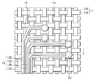
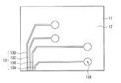
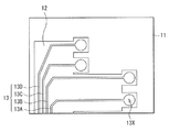
- FIG. 8A It is a cross-sectional schematic diagram showing an example of the wiring structure which concerns on one embodiment of this indication. It is a plane schematic diagram explaining an example of the wiring structure shown in FIG. It is a plane schematic diagram explaining the other example of the wiring structure shown in FIG. It is a plane schematic diagram explaining the other example of the wiring structure shown in FIG. It is a plane schematic diagram explaining the other example of the wiring structure shown in FIG. It is a plane schematic diagram explaining the other example of the wiring structure shown in FIG. It is a cross-sectional schematic diagram showing the other example of the wiring structure which concerns on one embodiment of this indication. It is a cross-sectional schematic diagram explaining the manufacturing process of the wiring structure shown in FIG. It is a cross-sectional schematic diagram following FIG. 8A.
- FIG. 8B It is a cross-sectional schematic diagram following an example of the wiring structure which concerns on the modification of this indication. It is a cross-sectional schematic diagram explaining the manufacturing process of the wiring structure shown in FIG. It is a cross-sectional schematic diagram following FIG. 10A. It is a cross-sectional schematic diagram following FIG. 10B. It is a cross-sectional schematic diagram following FIG. 10C. It is a cross-sectional schematic diagram following FIG. 11A. It is a cross-sectional schematic diagram showing the other example of the wiring structure which concerns on the modification of this indication.
- 12 is a perspective view illustrating an example of an appearance of application example 1.
- FIG. 12 is a perspective view illustrating an example of an appearance of application example 2.
- FIG. 22 is a perspective view illustrating another example of the appearance of application example 2.
- FIG. 12 is a perspective view illustrating an example of an appearance of application example 1.
- FIG. 12 is a perspective view illustrating an example of an appearance of application example 2.
- FIG. 22 is a
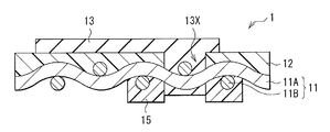
- FIG. 1 illustrates a cross-sectional configuration of a wiring structure (wiring structure 1) according to an embodiment of the present disclosure.
- FIG. 2 shows a planar configuration of the wiring structure 1, and the cross section of the wiring structure 1 shown in FIG. 1 corresponds to the line II in FIG.
- This wiring structure 1 is useful, for example, when wiring is formed on a stretchable substrate such as cloth.
- a wiring layer 13 is formed on the surface (surface S1) of the porous substrate 11 with a base layer 12 interposed.
- the wiring layer 13 has a through connection portion 13 ⁇ / b> X that penetrates to the back surface (surface S ⁇ b> 2) side of the porous substrate 11 through the opening 12 ⁇ / b> A provided in the base layer 12.
- 1 and 2 schematically illustrate an example of the configuration of the wiring structure 1, and may differ from actual dimensions and shapes.
- the porous substrate 11 is a porous substrate having elasticity, and fibrous materials (for example, fibers 11A and 11B) having a sufficient length with respect to the fiber diameter (diameter) are gathered and randomly overlapped.
- fibrous materials for example, fibers 11A and 11B
- it is a cloth-like three-dimensional structure formed.
- the cloth is an aggregate formed through a work of combining a plurality of fibers such as weaving and combing, and a cloth formed through a work of knitting by combining one or a plurality of fibers, or one It is an intertwined fiber.
- Specific examples include woven fabrics, knitted fabrics (knitted fabrics), laces, felts, and nonwoven fabrics.
- Examples of the constituent material of the porous substrate 11 include synthetic plastics such as polyester (PEs), polyethylene (PE), nylon, acrylic, polyurethane, and polytetrafluoroethylene (PTFE).
- Other examples include recycled fibers such as acetate rayon and cupra, natural fiber materials such as cotton, silk, hemp, and wool, and mixed materials thereof.
- a plurality of fibers 11A extending in the X-axis direction and a plurality of fibers 11B extending in the Z-axis direction are alternately intersected to form a porous material.
- the substrate 11 will be described as an example.
- the film thickness W (hereinafter simply referred to as thickness) of the porous substrate 11 in the Y-axis direction is, for example, 10 ⁇ m or more and 1000 ⁇ m or less.
- the thickness W of the porous substrate 11 in the present embodiment includes, for example, a fiber 11A and two fibers 11B that sandwich the fiber 11A alternately from above and below. If that is the case.
- the underlayer 12 flattens the surface of the porous substrate 11 and prevents the conductive material from spreading when forming the wiring layer 13, and provides fine wiring (for example, wiring 13 ⁇ / b> A, 13 ⁇ / b> B, 13 ⁇ / b> C, 13 ⁇ / b> D). It is for forming.
- a material for the underlayer 12 for example, a material having stretchability is preferably used. Examples of such materials include polyurethane resin, acrylic, polyacetal (POM), polyethylene (PE), polypropylene (PP), polystyrene (PS), polyvinyl chloride (PVC), polyester (PEs), and polyamide (PA).
- the base layer 12 can be formed by thermally transferring a sheet-like base resin, and the manufacturing process can be simplified.
- the thickness of the foundation layer 12 is, for example, 10 ⁇ m or more and 500 ⁇ m or less.
- the underlayer 12 may be patterned together with the patterns of the wirings 13 ⁇ / b> A, 13 ⁇ / b> B, 13 ⁇ / b> C, and 13 ⁇ / b> D, or as shown in FIG. 3, It may be provided on the entire surface. Alternatively, as shown in FIGS. 4, 5, and 6, it may be roughly patterned as long as it is formed at least between the porous substrate 11 and the wirings 13 ⁇ / b> A, 13 ⁇ / b> B, 13 ⁇ / b> C, 13 ⁇ / b> D. Good.
- the underlayer 12 can be formed by thermally transferring a sheet-like underlayer resin as described above, but in the sheet, the wiring layer 13 is located at a position where it penetrates to the back surface (surface S2) side of the porous substrate 11. It is preferable that an opening (for example, the opening 12A) is provided in advance.
- the wiring layer 13 includes a plurality of wirings, for example, wirings 13A, 13B, 13C, and 13D, and one end of each of the wirings 13A, 13B, 13C, and 13D,
- electrodes constituting the various sensors (sensor 120) are formed, and the other end is connected to, for example, a control unit (control unit 130) that controls the various sensors (see FIG. 13 for both).
- the wiring layer 13 is formed with a through connection portion 13 ⁇ / b> X that penetrates the porous substrate 11.
- the through connection portion 13X penetrates the porous base material 11, and for example, a portion penetrating to the back surface (surface S2) side of the porous base material 11 can be used as the electrode 13Y constituting the various sensors.
- the through connection portion 13X includes, for example, a wiring layer 13 formed on the front surface (surface S1) side of the porous substrate 11, and a wiring layer (for example, formed on the back surface (S2) side of the porous substrate 11) , And can be used as a through electrode for electrically connecting the wiring layer 23).
- the through connection portion 13 ⁇ / b> X is formed, for example, by soaking the wiring material constituting the wiring layer 13 into the porous substrate 11.
- the porous substrate 11 has a gap (pore 11a) continuous from the front surface S1 to the back surface S2 due to its structure.
- the through-connecting portion 13X is formed by allowing the wiring material to permeate through the pores 11a by capillary action.
- the through-connection portion 13X is configured to include the porous base material 11 therein, and the porous base material 11 in the through-connection portion 13X and the porous base material 11 in other regions are, for example, It has substantially the same density. Thereby, the mechanical strength of the penetration connection part 13X improves, and durability improves. Further, as shown in FIG.
- a base layer 15 is formed in advance at a corresponding position (for example, around the through-connection portion 13X) on the back surface S2 side of the porous substrate 11 where the through-connection portion 13X is formed. You may make it do. Thereby, it is possible to reduce the spread of the through-connection portion 13X on the back surface S2 side of the porous base material 11.
- the underlayer 15 may be provided on the entire back surface (surface S2) of the porous substrate 11.
- the wiring layer 13 is formed of a conductive wiring material.
- Specific wiring materials include, for example, poly (3,4-ethylenedioxythiophene) doped with polystyrene sulfonic acid (PPS) (PEDOT-PSS), PEDOT doped with p-toluenesulfonic acid (TsO) (PEDOT) -TsO) and other conductive polymers, silver nanoparticles, metal nanoparticles such as copper nanoparticles, metal nanowires such as silver nanowires and copper nanowires, metal pastes, carbon electrode materials such as carbon nanotubes, graphene and graphite, or These mixed materials are mentioned.
- the wiring layer 13 As a method for forming the wiring layer 13, for example, it is desirable to use a printing process such as screen printing, inkjet, gravure offset printing, reverse offset printing, flexographic printing, nanoimprinting, and dispenser. In addition, elastic metal wiring such as meandering metal wiring may be transferred. In that case, the through-connecting portion 13X is formed by patterning conductive ink separately by a process such as dispenser or inkjet.
- the protective layer 14 is for preventing corrosion and oxidation of the wiring layer 13 formed on the porous substrate 11.
- the protective layer 14 is formed of, for example, an epoxy resin, an acrylic resin, an imide resin, or a parylene resin.
- the thickness of the protective layer 14 should just be able to coat
- a polyethylene cloth is prepared as the porous substrate 11.
- a polyurethane sheet thickness 20 ⁇ m having an opening 12A formed at a position where the through-connecting portion 13X is formed by punching, for example, as the base layer 12, is formed by, for example, thermal lamination. Then, it is transferred onto the porous substrate 11 to form the underlayer 12.
- an ink solution containing, for example, a silver nanoparticle-containing polymer (PE873 manufactured by DuPont), as shown in FIG. 8B, using this ink solution, for example, the underlayer 12 and the opening are formed by screen printing.
- a wiring pattern is printed on the hole 12A. The wiring pattern exhibits conductivity by heating and drying, and the wiring layer 13 and the through connection portion 13X are formed.
- the ink solution is preferably adjusted for viscosity and surface energy.
- the solvent of the ink solution it is preferable to use an appropriate organic solvent in order to adjust the permeability to the porous substrate 11 (here, polyethylene cloth). What does not melt
- a petroleum solvent such as toluene and xylene.
- a protective layer 14 (PE773 manufactured by DuPont) that covers the wiring layer 13 is formed on the surface S1 side of the porous substrate 11 by, for example, spray coating. Thereby, the wiring structure 1 of the present embodiment is completed.
- the penetration connection part 13X penetrated to the back surface S2 side of the porous substrate 11 can be used as an electrode (electrode 13Y) of an electrochemical sensor, for example, by modifying the surface as necessary. .
- the wiring layer 13 is formed on the surface (surface S1) of the porous substrate 11 via the base layer 12. Thereby, the spread of the conductive material in the process of forming the wiring layer 13 is suppressed, and a fine wiring pattern can be formed.
- a technique for forming a multilayer wiring structure using a porous substrate for example, after forming a wiring pattern on the cloth, a through hole is formed in the cloth, and a conductive material is embedded in the through hole to form a back surface extraction electrode.
- Several methods have been reported. However, this method is difficult to industrialize.
- the back surface extraction electrode formed by this method has a conductive material unevenly distributed in the through holes, the mechanical characteristics of the back surface extraction electrode are greatly different from those of the surrounding fabric. As a result, cracks are likely to occur in the electrode (through electrode) portion in the through hole, and the reliability is expected to decrease.
- the through-connection portion 13X that includes the porous substrate 11 and penetrates from the front surface (surface S1) to the back surface (surface S2) of the porous substrate 11 is formed.
- the opening 12A is formed in advance at the position where the through connection portion 13X is formed when the base layer 12 is formed, the manufacturing process can be simplified.
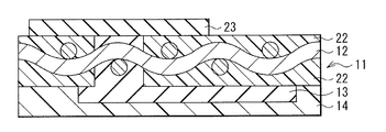
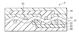
- FIG. 9 illustrates a cross-sectional configuration of a wiring structure (wiring structure 2) according to a modified example of the present disclosure.
- a base layer 22 is provided on the front surface (surface S1) and the back surface (surface S2) of the porous substrate 11, and the wiring layer 13 (surface S1 side) is provided on the base layer 22.
- the wiring layer 23 (surface S2 side) is formed respectively.
- the wiring layer 13 and the wiring layer 23 are electrically connected through the through connection portion 13X.
- a protective layer 14 and a protective layer 24 for protecting the wiring layer 13 and the wiring layer 23 are provided on the front surface (surface S1) and the back surface (surface S2) of the porous substrate 11, respectively.
- FIG. 9 schematically shows an example of the configuration of the wiring structure 2 and may differ from actual dimensions and shapes.
- the wiring layer 23 on the back surface (S2) side is provided via the base layer 22 as shown in FIG. Similar to the base layer 12 of the above-described embodiment, the base layer 22 flattens the surface of the porous substrate 11 and prevents the conductive material from spreading when forming the wiring layer 23. It is for forming.
- the material of the underlayer 22 include polyurethane resin, acrylic, polyacetal (POM), polyethylene (PE), polypropylene (PP), polystyrene (PS), polyvinyl chloride (PVC), polyester (PEs), polyamide (PA ), Polycarbonate (PC), phenol resin, epoxy resin, melamine resin, urea resin and silicone resin, or copolymers thereof.
- the underlayer 22 may be formed, for example, by thermally transferring a polyurethane sheet to the surface (surface S1) and the back surface (surface S2) of the porous substrate 11, respectively, like the underlayer 12 in the above embodiment.
- both the front surface (surface S1) and the back surface (surface S2) of the porous substrate 11 are collectively formed by spraying and infiltrating the porous substrate 11 with a solution containing the above materials. can do.
- the thickness of the foundation layer 22 is sufficient if the surface of the porous substrate 11 can be planarized.
- the thickness of the front surface (surface S1) and the back surface (surface S2) is preferably 10 ⁇ m or more and 1000 ⁇ m or less, respectively.
- the wiring layer 23 is formed of a wiring material having the same conductivity as that of the wiring layer 13. As described above, the wiring layer 23 is electrically connected to the wiring layer 13 via the through-connection portion 13X provided in the opening 22A formed in the base layer 22.
- the protective layer 24 is for preventing corrosion and oxidation of the wiring layer 23 and is formed of the same material as that of the protective layer 14.
- the thickness of the protective layer 24 is, for example, 1 ⁇ m or more and 100 ⁇ m or less, similarly to the protective layer 14.
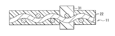
- a polyethylene cloth is prepared as the porous substrate 11, and as shown in FIG. 10A, the PVA aqueous solution is infiltrated into the formation position of the through connection portion 13X using, for example, a dispenser or an inkjet, and the mask 31 is attached. Form.
- the polyurethane resin solution is sprayed onto the porous base material 11 by, for example, spray coating, and permeated into the porous base material 11, and then the polyurethane resin is dried and solidified.
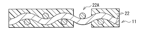
- the base layer 22 is collectively formed on the front surface (surface S1) and the back surface (surface S2) of the porous substrate 11.
- the mask 31 is removed to form the opening 22A.
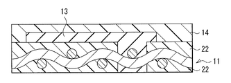
- the underlayer 22 and A wiring pattern is printed on the opening 22A.
- the wiring pattern exhibits conductivity by heating and drying, and the wiring layer 13 and the through connection portion 13X are formed.
- the protective layer 14 DuPont PE773 covering the wiring layer 13 is formed by, for example, spray coating.
- the porous substrate 11 is turned over, and the wiring layer 23 is formed on the base layer 22 on the back surface (S2) side by using the same method as the wiring layer 13 described above.
- a protective layer 24 (PE773 manufactured by DuPont) covering the wiring layer 23 is formed by, for example, spray coating, whereby the wiring structure 2 shown in FIG. 9 is completed.
- the base layer 22 in a part of back surface (surface S2) of the porous base material 11, as shown, for example in FIG.
- the base layer 12 shown in FIG. 2 may be patterned along a wiring pattern constituting the wiring layer 23.
- a polyurethane sheet in which the opening 12A (and the opening 22A) is formed on each of the display surface (surface S1) side and the back surface (surface S2) is formed by, for example, thermal lamination.
- the underlayer 12 and the underlayer 22 may be formed separately.
- the porous base material 22 is connected to the wiring layer 13 formed on the front surface (surface S1) side through the through connection portion 13X via the base layer 22. 11 on the back surface (surface S2). This makes it possible to form a multilayer wiring structure using a porous substrate having elasticity.
- FIG. 13 shows the appearance of the garment 110.
- the garment 110 includes, for example, various sensors 120 that detect or measure sweating, body temperature, sweat components, epidermal gas, blood sugar, and the like, a control unit 130 that controls the sensor 120, and a wiring 140 that connects the sensor 120 and the control unit. I have. Note that a circuit 150 may be provided in the middle of the wiring 140 between the sensor 120 and the control unit 130.
- the electrode and the wiring 140 constituting the sensor 120 are configured by the wiring structure 1 (or the wiring structure 2).
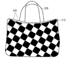
- FIG. 14A and FIG. 14B represent the appearance of a bag.
- the bag includes a cloth storage unit 210 and a handle 220, for example.
- a display body 230 including a display body such as an electrophoretic element is attached to the storage unit 210, for example.
- Various characters and designs are displayed on the storage unit 210 by the display body 230.
- the display body 230 may be attached not only to the storage unit 210 but also to the handle 220. For example, by applying a voltage, the display body 230 can change the design of the storage unit 210 from the example of FIG. 14A to the example of FIG. 14B.
- the wiring structure 1 (or the wiring structure 2) can be applied to a wiring that connects a control unit that controls display. Electronic devices that are useful in fashion applications can be realized.
- the present disclosure has been described with the embodiment and the modification.
- the present disclosure is not limited to the aspect described in the embodiment and the like, and various modifications are possible.
- the material and thickness of the component mentioned above are examples, and are not limited to what was described.
- the cloth 11A was shown as an example for the porous base material 11 by the two fibers 11B being alternately clamped from the upper direction and the downward direction, it is not restricted to this.
- the porous substrate 11 may be used by stacking two or more of the above-mentioned cloths, or may be a non-woven fabric in which a plurality of fibers are folded as described above.
- this indication can also take the following structures.
- Wiring structure with (2) A second conductive layer electrically connected to the first conductive layer via the through-connecting portion is provided on the other surface opposite to the one surface of the fibrous porous substrate.
- the density of the fibrous porous base material contained in the inside of the through-connecting portion and the density of the fibrous porous base material in other regions are substantially the same as described in (4).
- Wiring structure. The wiring structure according to any one of (2) to (5), wherein the fibrous porous substrate has pores continuous from the one surface to the other surface. (7) The wiring structure according to any one of (2) to (6), wherein the fibrous porous substrate has a second underlayer on the other surface. (8) The wiring structure according to (7), wherein the second base layer is provided around the through connection portion. (9) The wiring structure according to (7) or (8), wherein the second conductive layer is provided on the other surface of the fibrous porous substrate via the second base layer.
Landscapes
- Engineering & Computer Science (AREA)
- Microelectronics & Electronic Packaging (AREA)
- Textile Engineering (AREA)
- Printing Elements For Providing Electric Connections Between Printed Circuits (AREA)
- Laminated Bodies (AREA)
- Structure Of Printed Boards (AREA)
Abstract
Une structure de câblage d'un mode de réalisation de la présente invention comporte : un matériau de base poreux fibreux ; une première couche de masse formée sur une surface du matériau de base poreux fibreux ; et une première couche électroconductrice qui est disposée sur la première couche de masse et qui a une partie de connexion pénétrante qui pénètre dans le matériau de base poreux fibreux.
Applications Claiming Priority (2)
| Application Number | Priority Date | Filing Date | Title |
|---|---|---|---|
| JP2016-101036 | 2016-05-20 | ||
| JP2016101036A JP2017208492A (ja) | 2016-05-20 | 2016-05-20 | 配線構造および電子機器 |
Publications (1)
| Publication Number | Publication Date |
|---|---|
| WO2017199594A1 true WO2017199594A1 (fr) | 2017-11-23 |
Family
ID=60325924
Family Applications (1)
| Application Number | Title | Priority Date | Filing Date |
|---|---|---|---|
| PCT/JP2017/013298 Ceased WO2017199594A1 (fr) | 2016-05-20 | 2017-03-30 | Structure de câblage et dispositif électronique |
Country Status (2)
| Country | Link |
|---|---|
| JP (1) | JP2017208492A (fr) |
| WO (1) | WO2017199594A1 (fr) |
Cited By (1)
| Publication number | Priority date | Publication date | Assignee | Title |
|---|---|---|---|---|
| US11343910B2 (en) | 2018-06-07 | 2022-05-24 | The Governors Of The University Of Alberta | Elastic printed conductors |
Families Citing this family (3)
| Publication number | Priority date | Publication date | Assignee | Title |
|---|---|---|---|---|
| JP6960161B2 (ja) * | 2018-03-15 | 2021-11-05 | 国立研究開発法人科学技術振興機構 | 電子機能部材及び電子部品 |
| CN113166997B (zh) | 2018-12-26 | 2023-10-27 | 株式会社可乐丽 | 带有图案的纤维基材 |
| WO2026063286A1 (fr) * | 2024-09-18 | 2026-03-26 | 株式会社村田製作所 | Dispositif étirable et son procédé de fabrication |
Citations (4)
| Publication number | Priority date | Publication date | Assignee | Title |
|---|---|---|---|---|
| JPS5453264A (en) * | 1977-10-04 | 1979-04-26 | Suwa Seikosha Kk | Bilateral printed board |
| JP2001024081A (ja) * | 1999-07-08 | 2001-01-26 | Toshiba Corp | 導電基体及びその製造方法 |
| WO2006093016A1 (fr) * | 2005-02-28 | 2006-09-08 | So-Ken Co., Ltd. | Carte de circuit imprime et son procede de fabrication |
| JP2013187380A (ja) * | 2012-03-08 | 2013-09-19 | Nippon Mektron Ltd | 伸縮性フレキシブル回路基板およびその製造方法 |
-
2016
- 2016-05-20 JP JP2016101036A patent/JP2017208492A/ja active Pending
-
2017
- 2017-03-30 WO PCT/JP2017/013298 patent/WO2017199594A1/fr not_active Ceased
Patent Citations (4)
| Publication number | Priority date | Publication date | Assignee | Title |
|---|---|---|---|---|
| JPS5453264A (en) * | 1977-10-04 | 1979-04-26 | Suwa Seikosha Kk | Bilateral printed board |
| JP2001024081A (ja) * | 1999-07-08 | 2001-01-26 | Toshiba Corp | 導電基体及びその製造方法 |
| WO2006093016A1 (fr) * | 2005-02-28 | 2006-09-08 | So-Ken Co., Ltd. | Carte de circuit imprime et son procede de fabrication |
| JP2013187380A (ja) * | 2012-03-08 | 2013-09-19 | Nippon Mektron Ltd | 伸縮性フレキシブル回路基板およびその製造方法 |
Cited By (4)
| Publication number | Priority date | Publication date | Assignee | Title |
|---|---|---|---|---|
| US11343910B2 (en) | 2018-06-07 | 2022-05-24 | The Governors Of The University Of Alberta | Elastic printed conductors |
| EP3785497A4 (fr) * | 2018-06-07 | 2022-06-08 | The Governors Of The University Of Alberta | Conducteurs imprimés élastiques |
| US20220256693A1 (en) * | 2018-06-07 | 2022-08-11 | The Governors Of The University Of Alberta | Elastic printed conductors |
| US11849540B2 (en) | 2018-06-07 | 2023-12-19 | The Governors Of The University Of Alberta | Elastic printed conductors |
Also Published As
| Publication number | Publication date |
|---|---|
| JP2017208492A (ja) | 2017-11-24 |
Similar Documents
| Publication | Publication Date | Title |
|---|---|---|
| Castano et al. | Smart fabric sensors and e-textile technologies: a review | |
| Zheng et al. | MXene functionalized, highly breathable and sensitive pressure sensors with multi‐layered porous structure | |
| US20190297960A1 (en) | Methods and compositions for wearable textile electronic devices | |
| Chen et al. | Permeable conductors for wearable and on‐skin electronics | |
| US20090286055A1 (en) | Methods and Devices for Providing Flexible Electronics | |
| JP6454649B2 (ja) | 電極部材および装置 | |
| Raman et al. | Intrinsically conducting polymers in flexible and stretchable resistive strain sensors: a review | |
| US10251266B2 (en) | Wearable flexible printed circuit board and method of manufacturing the same | |
| JP2017208492A (ja) | 配線構造および電子機器 | |
| Guo et al. | Pressure regulated printing of semiliquid metal on electrospinning film enables breathable and waterproof wearable electronics | |
| TWI581758B (zh) | 布膜生理感測器 | |
| Liman et al. | Emerging washable textronics for imminent e-waste mitigation: strategies, reliability, and perspectives | |
| JP2009518209A5 (fr) | ||
| Zhang et al. | Smart wearable fibers and textiles: status and prospects | |
| JP6999139B2 (ja) | アンテナ、無線通信装置、生体信号測定装置、および衣服 | |
| JP6168507B1 (ja) | 導電性生地 | |
| KR102807199B1 (ko) | 패턴 형성된 섬유 기재 | |
| KR101938214B1 (ko) | 전기 전도성 원단 및 이의 제조방법 | |
| KR101691381B1 (ko) | 발열원단 및 이의 제조방법 | |
| KR101102840B1 (ko) | 방수, 투습, 및 제전성을 가진 면상 발열체 및 이의 제조방법 | |
| Maity et al. | Advanced applications of green materials in wearable e-textiles | |
| KR20110109716A (ko) | 전도성 원단 및 이의 제조방법 | |
| Agarwala | Enabling new possibilities in smart textiles through printed electronics | |
| JP6168506B1 (ja) | 導電性生地及びその製造方法 | |
| JP2021190500A (ja) | 配線付き繊維部材及びその製造方法 |
Legal Events
| Date | Code | Title | Description |
|---|---|---|---|
| NENP | Non-entry into the national phase |
Ref country code: DE |
|
| 121 | Ep: the epo has been informed by wipo that ep was designated in this application |
Ref document number: 17799028 Country of ref document: EP Kind code of ref document: A1 |
|
| 122 | Ep: pct application non-entry in european phase |
Ref document number: 17799028 Country of ref document: EP Kind code of ref document: A1 |