WO2017199829A1 - Procédé de fabrication de carte stratifiée à revêtement métallique, procédé de fabrication de carte de circuit électronique et dispositif de mesure de viscoélasticité de type pendule à corps rigide - Google Patents
Procédé de fabrication de carte stratifiée à revêtement métallique, procédé de fabrication de carte de circuit électronique et dispositif de mesure de viscoélasticité de type pendule à corps rigide Download PDFInfo
- Publication number
- WO2017199829A1 WO2017199829A1 PCT/JP2017/017792 JP2017017792W WO2017199829A1 WO 2017199829 A1 WO2017199829 A1 WO 2017199829A1 JP 2017017792 W JP2017017792 W JP 2017017792W WO 2017199829 A1 WO2017199829 A1 WO 2017199829A1
- Authority
- WO
- WIPO (PCT)
- Prior art keywords
- liquid crystal
- crystal polymer
- polymer film
- pendulum
- metal
- Prior art date
- Legal status (The legal status is an assumption and is not a legal conclusion. Google has not performed a legal analysis and makes no representation as to the accuracy of the status listed.)
- Ceased
Links
Images


Classifications
-
- H—ELECTRICITY
- H05—ELECTRIC TECHNIQUES NOT OTHERWISE PROVIDED FOR
- H05K—PRINTED CIRCUITS; CASINGS OR CONSTRUCTIONAL DETAILS OF ELECTRIC APPARATUS; MANUFACTURE OF ASSEMBLAGES OF ELECTRICAL COMPONENTS
- H05K3/00—Apparatus or processes for manufacturing printed circuits
- H05K3/46—Manufacturing multilayer circuits
- H05K3/4611—Manufacturing multilayer circuits by laminating two or more circuit boards
- H05K3/4626—Manufacturing multilayer circuits by laminating two or more circuit boards characterised by the insulating layers or materials
- H05K3/4632—Manufacturing multilayer circuits by laminating two or more circuit boards characterised by the insulating layers or materials laminating thermoplastic or uncured resin sheets comprising printed circuits without added adhesive materials between the sheets
-
- B—PERFORMING OPERATIONS; TRANSPORTING
- B32—LAYERED PRODUCTS
- B32B—LAYERED PRODUCTS, i.e. PRODUCTS BUILT-UP OF STRATA OF FLAT OR NON-FLAT, e.g. CELLULAR OR HONEYCOMB, FORM
- B32B15/00—Layered products comprising a layer of metal
- B32B15/04—Layered products comprising a layer of metal comprising metal as the main or only constituent of a layer, which is next to another layer of the same or of a different material
- B32B15/08—Layered products comprising a layer of metal comprising metal as the main or only constituent of a layer, which is next to another layer of the same or of a different material of synthetic resin
- B32B15/092—Layered products comprising a layer of metal comprising metal as the main or only constituent of a layer, which is next to another layer of the same or of a different material of synthetic resin comprising epoxy resins
-
- B—PERFORMING OPERATIONS; TRANSPORTING
- B32—LAYERED PRODUCTS
- B32B—LAYERED PRODUCTS, i.e. PRODUCTS BUILT-UP OF STRATA OF FLAT OR NON-FLAT, e.g. CELLULAR OR HONEYCOMB, FORM
- B32B15/00—Layered products comprising a layer of metal
- B32B15/04—Layered products comprising a layer of metal comprising metal as the main or only constituent of a layer, which is next to another layer of the same or of a different material
- B32B15/08—Layered products comprising a layer of metal comprising metal as the main or only constituent of a layer, which is next to another layer of the same or of a different material of synthetic resin
- B32B15/088—Layered products comprising a layer of metal comprising metal as the main or only constituent of a layer, which is next to another layer of the same or of a different material of synthetic resin comprising polyamides
-
- B—PERFORMING OPERATIONS; TRANSPORTING
- B32—LAYERED PRODUCTS
- B32B—LAYERED PRODUCTS, i.e. PRODUCTS BUILT-UP OF STRATA OF FLAT OR NON-FLAT, e.g. CELLULAR OR HONEYCOMB, FORM
- B32B15/00—Layered products comprising a layer of metal
- B32B15/04—Layered products comprising a layer of metal comprising metal as the main or only constituent of a layer, which is next to another layer of the same or of a different material
- B32B15/08—Layered products comprising a layer of metal comprising metal as the main or only constituent of a layer, which is next to another layer of the same or of a different material of synthetic resin
- B32B15/09—Layered products comprising a layer of metal comprising metal as the main or only constituent of a layer, which is next to another layer of the same or of a different material of synthetic resin comprising polyesters
-
- B—PERFORMING OPERATIONS; TRANSPORTING
- B32—LAYERED PRODUCTS
- B32B—LAYERED PRODUCTS, i.e. PRODUCTS BUILT-UP OF STRATA OF FLAT OR NON-FLAT, e.g. CELLULAR OR HONEYCOMB, FORM
- B32B15/00—Layered products comprising a layer of metal
- B32B15/18—Layered products comprising a layer of metal comprising iron or steel
-
- B—PERFORMING OPERATIONS; TRANSPORTING
- B32—LAYERED PRODUCTS
- B32B—LAYERED PRODUCTS, i.e. PRODUCTS BUILT-UP OF STRATA OF FLAT OR NON-FLAT, e.g. CELLULAR OR HONEYCOMB, FORM
- B32B15/00—Layered products comprising a layer of metal
- B32B15/20—Layered products comprising a layer of metal comprising aluminium or copper
-
- B—PERFORMING OPERATIONS; TRANSPORTING
- B32—LAYERED PRODUCTS
- B32B—LAYERED PRODUCTS, i.e. PRODUCTS BUILT-UP OF STRATA OF FLAT OR NON-FLAT, e.g. CELLULAR OR HONEYCOMB, FORM
- B32B27/00—Layered products comprising a layer of synthetic resin
- B32B27/06—Layered products comprising a layer of synthetic resin as the main or only constituent of a layer, which is next to another layer of the same or of a different material
- B32B27/08—Layered products comprising a layer of synthetic resin as the main or only constituent of a layer, which is next to another layer of the same or of a different material of synthetic resin
-
- B—PERFORMING OPERATIONS; TRANSPORTING
- B32—LAYERED PRODUCTS
- B32B—LAYERED PRODUCTS, i.e. PRODUCTS BUILT-UP OF STRATA OF FLAT OR NON-FLAT, e.g. CELLULAR OR HONEYCOMB, FORM
- B32B27/00—Layered products comprising a layer of synthetic resin
- B32B27/28—Layered products comprising a layer of synthetic resin comprising synthetic resins not wholly covered by any one of the sub-groups B32B27/30 - B32B27/42
- B32B27/281—Layered products comprising a layer of synthetic resin comprising synthetic resins not wholly covered by any one of the sub-groups B32B27/30 - B32B27/42 comprising polyimides
-
- B—PERFORMING OPERATIONS; TRANSPORTING
- B32—LAYERED PRODUCTS
- B32B—LAYERED PRODUCTS, i.e. PRODUCTS BUILT-UP OF STRATA OF FLAT OR NON-FLAT, e.g. CELLULAR OR HONEYCOMB, FORM
- B32B27/00—Layered products comprising a layer of synthetic resin
- B32B27/34—Layered products comprising a layer of synthetic resin comprising polyamides
-
- B—PERFORMING OPERATIONS; TRANSPORTING
- B32—LAYERED PRODUCTS
- B32B—LAYERED PRODUCTS, i.e. PRODUCTS BUILT-UP OF STRATA OF FLAT OR NON-FLAT, e.g. CELLULAR OR HONEYCOMB, FORM
- B32B27/00—Layered products comprising a layer of synthetic resin
- B32B27/38—Layered products comprising a layer of synthetic resin comprising epoxy resins
-
- B—PERFORMING OPERATIONS; TRANSPORTING
- B32—LAYERED PRODUCTS
- B32B—LAYERED PRODUCTS, i.e. PRODUCTS BUILT-UP OF STRATA OF FLAT OR NON-FLAT, e.g. CELLULAR OR HONEYCOMB, FORM
- B32B3/00—Layered products comprising a layer with external or internal discontinuities or unevennesses, or a layer of non-planar shape; Layered products comprising a layer having particular features of form
- B32B3/02—Layered products comprising a layer with external or internal discontinuities or unevennesses, or a layer of non-planar shape; Layered products comprising a layer having particular features of form characterised by features of form at particular places, e.g. in edge regions
- B32B3/08—Layered products comprising a layer with external or internal discontinuities or unevennesses, or a layer of non-planar shape; Layered products comprising a layer having particular features of form characterised by features of form at particular places, e.g. in edge regions characterised by added members at particular parts
-
- B—PERFORMING OPERATIONS; TRANSPORTING
- B32—LAYERED PRODUCTS
- B32B—LAYERED PRODUCTS, i.e. PRODUCTS BUILT-UP OF STRATA OF FLAT OR NON-FLAT, e.g. CELLULAR OR HONEYCOMB, FORM
- B32B38/00—Ancillary operations in connection with laminating processes
- B32B38/18—Handling of layers or the laminate
-
- B—PERFORMING OPERATIONS; TRANSPORTING
- B32—LAYERED PRODUCTS
- B32B—LAYERED PRODUCTS, i.e. PRODUCTS BUILT-UP OF STRATA OF FLAT OR NON-FLAT, e.g. CELLULAR OR HONEYCOMB, FORM
- B32B5/00—Layered products characterised by the non- homogeneity or physical structure, i.e. comprising a fibrous, filamentary, particulate or foam layer; Layered products characterised by having a layer differing constitutionally or physically in different parts
- B32B5/14—Layered products characterised by the non- homogeneity or physical structure, i.e. comprising a fibrous, filamentary, particulate or foam layer; Layered products characterised by having a layer differing constitutionally or physically in different parts characterised by a layer differing constitutionally or physically in different parts, e.g. denser near its faces
-
- B—PERFORMING OPERATIONS; TRANSPORTING
- B32—LAYERED PRODUCTS
- B32B—LAYERED PRODUCTS, i.e. PRODUCTS BUILT-UP OF STRATA OF FLAT OR NON-FLAT, e.g. CELLULAR OR HONEYCOMB, FORM
- B32B7/00—Layered products characterised by the relation between layers; Layered products characterised by the relative orientation of features between layers, or by the relative values of a measurable parameter between layers, i.e. products comprising layers having different physical, chemical or physicochemical properties; Layered products characterised by the interconnection of layers
- B32B7/04—Interconnection of layers
- B32B7/06—Interconnection of layers permitting easy separation
-
- H—ELECTRICITY
- H05—ELECTRIC TECHNIQUES NOT OTHERWISE PROVIDED FOR
- H05K—PRINTED CIRCUITS; CASINGS OR CONSTRUCTIONAL DETAILS OF ELECTRIC APPARATUS; MANUFACTURE OF ASSEMBLAGES OF ELECTRICAL COMPONENTS
- H05K3/00—Apparatus or processes for manufacturing printed circuits
- H05K3/38—Improvement of the adhesion between the insulating substrate and the metal
- H05K3/381—Improvement of the adhesion between the insulating substrate and the metal by special treatment of the substrate
-
- B—PERFORMING OPERATIONS; TRANSPORTING
- B32—LAYERED PRODUCTS
- B32B—LAYERED PRODUCTS, i.e. PRODUCTS BUILT-UP OF STRATA OF FLAT OR NON-FLAT, e.g. CELLULAR OR HONEYCOMB, FORM
- B32B2250/00—Layers arrangement
- B32B2250/02—2 layers
-
- B—PERFORMING OPERATIONS; TRANSPORTING
- B32—LAYERED PRODUCTS
- B32B—LAYERED PRODUCTS, i.e. PRODUCTS BUILT-UP OF STRATA OF FLAT OR NON-FLAT, e.g. CELLULAR OR HONEYCOMB, FORM
- B32B2250/00—Layers arrangement
- B32B2250/03—3 layers
-
- B—PERFORMING OPERATIONS; TRANSPORTING
- B32—LAYERED PRODUCTS
- B32B—LAYERED PRODUCTS, i.e. PRODUCTS BUILT-UP OF STRATA OF FLAT OR NON-FLAT, e.g. CELLULAR OR HONEYCOMB, FORM
- B32B2250/00—Layers arrangement
- B32B2250/40—Symmetrical or sandwich layers, e.g. ABA, ABCBA, ABCCBA
-
- B—PERFORMING OPERATIONS; TRANSPORTING
- B32—LAYERED PRODUCTS
- B32B—LAYERED PRODUCTS, i.e. PRODUCTS BUILT-UP OF STRATA OF FLAT OR NON-FLAT, e.g. CELLULAR OR HONEYCOMB, FORM
- B32B2307/00—Properties of the layers or laminate
- B32B2307/30—Properties of the layers or laminate having particular thermal properties
- B32B2307/306—Resistant to heat
-
- B—PERFORMING OPERATIONS; TRANSPORTING
- B32—LAYERED PRODUCTS
- B32B—LAYERED PRODUCTS, i.e. PRODUCTS BUILT-UP OF STRATA OF FLAT OR NON-FLAT, e.g. CELLULAR OR HONEYCOMB, FORM
- B32B2307/00—Properties of the layers or laminate
- B32B2307/40—Properties of the layers or laminate having particular optical properties
- B32B2307/408—Matt, dull surface
-
- B—PERFORMING OPERATIONS; TRANSPORTING
- B32—LAYERED PRODUCTS
- B32B—LAYERED PRODUCTS, i.e. PRODUCTS BUILT-UP OF STRATA OF FLAT OR NON-FLAT, e.g. CELLULAR OR HONEYCOMB, FORM
- B32B2307/00—Properties of the layers or laminate
- B32B2307/50—Properties of the layers or laminate having particular mechanical properties
- B32B2307/538—Roughness
-
- B—PERFORMING OPERATIONS; TRANSPORTING
- B32—LAYERED PRODUCTS
- B32B—LAYERED PRODUCTS, i.e. PRODUCTS BUILT-UP OF STRATA OF FLAT OR NON-FLAT, e.g. CELLULAR OR HONEYCOMB, FORM
- B32B2307/00—Properties of the layers or laminate
- B32B2307/70—Other properties
- B32B2307/732—Dimensional properties
-
- B—PERFORMING OPERATIONS; TRANSPORTING
- B32—LAYERED PRODUCTS
- B32B—LAYERED PRODUCTS, i.e. PRODUCTS BUILT-UP OF STRATA OF FLAT OR NON-FLAT, e.g. CELLULAR OR HONEYCOMB, FORM
- B32B2307/00—Properties of the layers or laminate
- B32B2307/70—Other properties
- B32B2307/748—Releasability
-
- B—PERFORMING OPERATIONS; TRANSPORTING
- B32—LAYERED PRODUCTS
- B32B—LAYERED PRODUCTS, i.e. PRODUCTS BUILT-UP OF STRATA OF FLAT OR NON-FLAT, e.g. CELLULAR OR HONEYCOMB, FORM
- B32B2457/00—Electrical equipment
- B32B2457/08—PCBs, i.e. printed circuit boards
-
- B—PERFORMING OPERATIONS; TRANSPORTING
- B32—LAYERED PRODUCTS
- B32B—LAYERED PRODUCTS, i.e. PRODUCTS BUILT-UP OF STRATA OF FLAT OR NON-FLAT, e.g. CELLULAR OR HONEYCOMB, FORM
- B32B27/00—Layered products comprising a layer of synthetic resin
- B32B27/36—Layered products comprising a layer of synthetic resin comprising polyesters
-
- H—ELECTRICITY
- H05—ELECTRIC TECHNIQUES NOT OTHERWISE PROVIDED FOR
- H05K—PRINTED CIRCUITS; CASINGS OR CONSTRUCTIONAL DETAILS OF ELECTRIC APPARATUS; MANUFACTURE OF ASSEMBLAGES OF ELECTRICAL COMPONENTS
- H05K2201/00—Indexing scheme relating to printed circuits covered by H05K1/00
- H05K2201/01—Dielectrics
- H05K2201/0137—Materials
- H05K2201/0141—Liquid crystal polymer [LCP]
-
- Y—GENERAL TAGGING OF NEW TECHNOLOGICAL DEVELOPMENTS; GENERAL TAGGING OF CROSS-SECTIONAL TECHNOLOGIES SPANNING OVER SEVERAL SECTIONS OF THE IPC; TECHNICAL SUBJECTS COVERED BY FORMER USPC CROSS-REFERENCE ART COLLECTIONS [XRACs] AND DIGESTS
- Y02—TECHNOLOGIES OR APPLICATIONS FOR MITIGATION OR ADAPTATION AGAINST CLIMATE CHANGE
- Y02E—REDUCTION OF GREENHOUSE GAS [GHG] EMISSIONS, RELATED TO ENERGY GENERATION, TRANSMISSION OR DISTRIBUTION
- Y02E10/00—Energy generation through renewable energy sources
- Y02E10/50—Photovoltaic [PV] energy
-
- Y—GENERAL TAGGING OF NEW TECHNOLOGICAL DEVELOPMENTS; GENERAL TAGGING OF CROSS-SECTIONAL TECHNOLOGIES SPANNING OVER SEVERAL SECTIONS OF THE IPC; TECHNICAL SUBJECTS COVERED BY FORMER USPC CROSS-REFERENCE ART COLLECTIONS [XRACs] AND DIGESTS
- Y02—TECHNOLOGIES OR APPLICATIONS FOR MITIGATION OR ADAPTATION AGAINST CLIMATE CHANGE
- Y02P—CLIMATE CHANGE MITIGATION TECHNOLOGIES IN THE PRODUCTION OR PROCESSING OF GOODS
- Y02P70/00—Climate change mitigation technologies in the production process for final industrial or consumer products
- Y02P70/50—Manufacturing or production processes characterised by the final manufactured product
Definitions
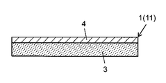
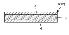
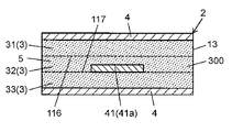
- the liquid crystal polymer film 3 includes a first liquid crystal polymer film 31, a second liquid crystal polymer film 32, and a third liquid crystal polymer film 33.
- the second liquid crystal polymer film 32 is adjacent to the first liquid crystal polymer film 31 and the third liquid crystal polymer film 33.
- the conductor circuit 41 is provided between the adjacent second liquid crystal polymer film 32 and third liquid crystal polymer film 33.
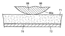
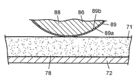
- a displacement piece 85 is provided between the lower side of the frame portion 81 and the vibration piece 84.
- the displacement piece 85 is a reference for measuring the displacement of the pendulum 8.
- the sample stage 72 on which the sample 71 is placed is inserted into the opening 83 of the pendulum 8, and the fulcrum portion 86 of the pendulum 8 is placed on the sample 71.
- the fulcrum part 86 is brought into contact with the sample 71. In this state, the pendulum 8 can be freely vibrated using the fulcrum portion 86 as a fulcrum.
- the vibration device 74 is configured to apply vibration to the pendulum 8.
- the vibration device 74 includes an electromagnet 74a and a power source 74b.
- the electromagnet 74a is provided at a position facing the excitation piece 84 when the pendulum 8 is stationary.
- the power source 74b is electrically connected to the electromagnet 74a and the control device 75. Energization of the power supply 74b to the electromagnet 74a is controlled by the control device 75.
- the electromagnet 74a is energized and the energization is stopped after the vibrating piece 84 is attracted to the electromagnet 74a, the pendulum 8 can be vibrated.
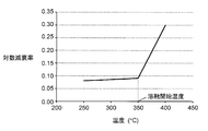
- FIG. 6 is a diagram showing an example of deriving the melting start temperature from the logarithmic decay rate of the liquid crystal polymer film in the embodiment.
- the sample 71 is raised from 250 ° C. by 1 ° C. by the heating device 78.
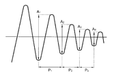
- the rigid pendulum type viscoelasticity measuring device 7 the logarithmic decay rate at each temperature of the sample 71 is measured.
- the temperature at which the slope changes is the melting start temperature of the sample 71.
- the slope based on the relationship between each temperature and the logarithmic decay rate changes around 350 ° C., so 350 ° C. is the melting start temperature of the sample 71.
- the step of preparing the core material 6 having the conductor circuit 41 formed on one side, and the metal foil 4 is attached to one side of the first liquid crystal polymer film 31.
- a step of preparing the single-sided metal-clad laminate 11, a step of preparing the bonding sheet 5 composed of the second liquid crystal polymer film 32, a step of removing the outermost layers on both sides of the second liquid crystal polymer film 32, a core The surface of the material 6 on which the conductor circuit 41 is formed and one surface of the bonding sheet 5 face each other, and the other surface of the bonding sheet 5 and the first liquid crystal polymer film 31 of the single-sided metal-clad laminate 11
- a step of producing the laminate 13 by sequentially stacking the core material 6, the bonding sheet 5 and the single-sided metal-clad laminate 11 so as to face each other, and a step of heating and pressing the laminate 13.
- the measurement using the rigid pendulum type viscoelasticity measuring device 7 is based on the motion characteristics of the pendulum 8 when the fulcrum portion 86 of the pendulum 8 is brought into contact with the second liquid crystal polymer film 32 as the sample 71 and the pendulum 8 is vibrated. Done.
- the fulcrum part 86 of the pendulum 8 is a cylindrical rod 88 with the metal foil 4 attached to the outer surface, and the metal foil 4 is attached to the rod 88 so that the roughened surface is on the outside. It is preferable.
- the liquid crystal polymer film 3 from which the uppermost liquid crystal polymer layer on the upper and lower surfaces was removed was set as a sample 71 in the rigid pendulum viscoelasticity measuring device 7.
- the melting start temperature of the upper and lower surfaces of the liquid crystal polymer film 3 and the logarithmic decay rate at 250 ° C. were measured.
- the melting start temperature on the upper surface was 325 ° C.
- the melting start temperature on the lower surface was 320 ° C.
- the logarithmic decay rate at 250 ° C. was 0.08.
- the melting start temperature on both sides of the liquid crystal polymer film 3 before polishing and the logarithmic decay rate at 250 ° C. were the same as in Example 1.
- the bonding sheet 5 from which the outermost liquid crystal polymer layer on the upper and lower surfaces was removed was set as a sample 71 in the rigid pendulum type viscoelasticity measuring device 7.
- the melting start temperatures of the upper and lower surfaces of the second liquid crystal polymer film 32 and the logarithmic decay rate at 250 ° C. were measured.
- the melting start temperature on the upper surface was 280 ° C.
- the melting start temperature on the lower surface was 295 ° C.
- the logarithmic decay rate at 250 ° C. was 0.09.
- the electronic circuit board 2 was manufactured by the same method as in Example 3 using the single-sided metal-clad laminate 11, the bonding sheet 5, and the core material 6.
- the same liquid crystal polymer film as in Example 3 (“Kexar CT-F” manufactured by Kuraray Co., Ltd.) was prepared.
- the bonding sheet 5 at this stage is not treated to remove the outermost liquid crystal polymer layer.
- a double-sided metal-clad laminate 12 was produced in the same manner as in Example 1 using the liquid crystal polymer film 3 that had not been subjected to the treatment for removing the outermost liquid crystal polymer layer.
- the present invention when a metal-clad laminate including a liquid crystal polymer film is produced, the adhesion between the liquid crystal polymer film and the metal foil can be improved. Moreover, when manufacturing the electronic circuit board containing a liquid crystal polymer film, the adhesiveness of a liquid crystal polymer film and a conductor circuit can be improved. Therefore, the present invention is industrially useful as a method for producing a metal-clad laminate and an electronic circuit board.
Landscapes
- Engineering & Computer Science (AREA)
- Manufacturing & Machinery (AREA)
- Microelectronics & Electronic Packaging (AREA)
- Laminated Bodies (AREA)
- Manufacturing Of Printed Wiring (AREA)
Abstract
La présente invention comprend : une étape de retrait de la couche extérieure d'une surface ou des deux surfaces d'un film de polymère à cristaux liquides (3) ; et une étape de moulage dans laquelle une feuille métallique (4) est recouverte sur la surface pour laquelle la couche extérieure du film de polymère à cristaux liquides (3) a été retirée, et un moulage à la presse à chaud est effectué. La température de chauffage pour l'étape de moulage est dans une plage de la même température ou plus élevée que la température de début de fusion du film de polymère à cristaux liquides (3) et une température non supérieure de plus de 60 °C à la température de début de fusion du film de polymère à cristaux liquides (3), mesurée au moyen d'un dispositif de mesure de viscoélasticité de type pendule à corps rigide.
Priority Applications (3)
| Application Number | Priority Date | Filing Date | Title |
|---|---|---|---|
| CN201780029877.5A CN109196962B (zh) | 2016-05-20 | 2017-05-11 | 覆金属层叠板的制造方法、电子电路基板的制造方法、刚体振子型粘弹性测定装置 |
| US16/094,044 US10668697B2 (en) | 2016-05-20 | 2017-05-11 | Method for manufacturing metal clad laminated board, method for manufacturing electronic circuit board, and rigid body pendulum type viscoelasticity measuring device |
| JP2018518247A JP7178634B2 (ja) | 2016-05-20 | 2017-05-11 | 金属張積層板の製造方法、電子回路基板の製造方法 |
Applications Claiming Priority (2)
| Application Number | Priority Date | Filing Date | Title |
|---|---|---|---|
| JP2016-101985 | 2016-05-20 | ||
| JP2016101985 | 2016-05-20 |
Publications (1)
| Publication Number | Publication Date |
|---|---|
| WO2017199829A1 true WO2017199829A1 (fr) | 2017-11-23 |
Family
ID=60324955
Family Applications (1)
| Application Number | Title | Priority Date | Filing Date |
|---|---|---|---|
| PCT/JP2017/017792 Ceased WO2017199829A1 (fr) | 2016-05-20 | 2017-05-11 | Procédé de fabrication de carte stratifiée à revêtement métallique, procédé de fabrication de carte de circuit électronique et dispositif de mesure de viscoélasticité de type pendule à corps rigide |
Country Status (5)
| Country | Link |
|---|---|
| US (1) | US10668697B2 (fr) |
| JP (1) | JP7178634B2 (fr) |
| CN (1) | CN109196962B (fr) |
| TW (1) | TWI738777B (fr) |
| WO (1) | WO2017199829A1 (fr) |
Cited By (3)
| Publication number | Priority date | Publication date | Assignee | Title |
|---|---|---|---|---|
| WO2018221500A1 (fr) * | 2017-05-31 | 2018-12-06 | パナソニックIpマネジメント株式会社 | Stratifié à revêtement métallique et procédé de fabrication associé |
| WO2019082971A1 (fr) * | 2017-10-26 | 2019-05-02 | パナソニックIpマネジメント株式会社 | Stratifié à revêtement métallique et procédé de fabrication associé |
| WO2021215353A1 (fr) * | 2020-04-22 | 2021-10-28 | 東洋鋼鈑株式会社 | Film stratifié métallique et son procédé de fabrication |
Families Citing this family (3)
| Publication number | Priority date | Publication date | Assignee | Title |
|---|---|---|---|---|
| CN108712962A (zh) * | 2016-03-08 | 2018-10-26 | 株式会社可乐丽 | 覆金属层叠板的制造方法和覆金属层叠板 |
| JP7182030B2 (ja) * | 2020-03-24 | 2022-12-01 | 株式会社クラレ | 金属張積層体の製造方法 |
| US12057248B2 (en) * | 2020-06-17 | 2024-08-06 | Nippon Steel Corporation | Electrical steel sheet, laminated core and rotating electric machine |
Citations (5)
| Publication number | Priority date | Publication date | Assignee | Title |
|---|---|---|---|---|
| JPS481988U (fr) * | 1971-05-25 | 1973-01-11 | ||
| JP2004339330A (ja) * | 2003-05-14 | 2004-12-02 | Dainippon Printing Co Ltd | 熱硬化性インク用顔料分散液、熱硬化性インク、カラーフィルターの製造方法、カラーフィルター、及び表示パネル |
| JP2008109127A (ja) * | 2006-09-29 | 2008-05-08 | Nippon Steel Chem Co Ltd | フレキシブル基板の製造方法 |
| JP2010103269A (ja) * | 2008-10-23 | 2010-05-06 | Kuraray Co Ltd | 多層回路基板およびその製造方法 |
| JP2016010967A (ja) * | 2014-06-05 | 2016-01-21 | パナソニックIpマネジメント株式会社 | 金属箔付き液晶ポリマーフィルムの製造方法、金属箔付き液晶ポリマーフィルム、多層プリント配線板の製造方法 |
Family Cites Families (11)
| Publication number | Priority date | Publication date | Assignee | Title |
|---|---|---|---|---|
| JPH0610293Y2 (ja) * | 1986-08-25 | 1994-03-16 | 株式会社オリエンテック | 剛体振子型2次転移点測定器 |
| US5085015A (en) * | 1990-06-26 | 1992-02-04 | E. I. Du Pont De Nemours And Company | Process for improving the surface of liquid crystal polymers |
| JP4162321B2 (ja) * | 1999-03-18 | 2008-10-08 | 株式会社クラレ | 金属箔積層板の製造方法 |
| JP2005081649A (ja) | 2003-09-08 | 2005-03-31 | Toray Eng Co Ltd | 液晶ポリマーフィルム積層基材の製造方法 |
| US8771458B2 (en) * | 2005-07-27 | 2014-07-08 | Kuraray Co., Ltd. | Method of making wiring boards covered by thermotropic liquid crystal polymer film |
| JP4793080B2 (ja) * | 2006-04-26 | 2011-10-12 | 凸版印刷株式会社 | ポリエチレンテレフタレート表面の結晶化度の算出方法 |
| TW200820853A (en) * | 2006-09-29 | 2008-05-01 | Nippon Steel Chemical Co | Manufacturing method of flexible substrate |
| JP5411656B2 (ja) * | 2009-02-24 | 2014-02-12 | パナソニック株式会社 | フレキシブルプリント配線板用積層板の製造方法、フレキシブルプリント配線板用積層板及びフレキシブルプリント配線板 |
| KR20120124449A (ko) | 2010-01-29 | 2012-11-13 | 신닛테츠가가쿠 가부시키가이샤 | 편면 금속장 적층체의 제조방법 |
| JP2012219045A (ja) * | 2011-04-06 | 2012-11-12 | Nitto Denko Corp | 貼付剤および貼付製剤 |
| JP5654416B2 (ja) * | 2011-06-07 | 2015-01-14 | Jx日鉱日石金属株式会社 | 液晶ポリマー銅張積層板及び当該積層板に用いる銅箔 |
-
2017
- 2017-05-11 JP JP2018518247A patent/JP7178634B2/ja active Active
- 2017-05-11 WO PCT/JP2017/017792 patent/WO2017199829A1/fr not_active Ceased
- 2017-05-11 US US16/094,044 patent/US10668697B2/en active Active
- 2017-05-11 CN CN201780029877.5A patent/CN109196962B/zh active Active
- 2017-05-12 TW TW106115774A patent/TWI738777B/zh active
Patent Citations (5)
| Publication number | Priority date | Publication date | Assignee | Title |
|---|---|---|---|---|
| JPS481988U (fr) * | 1971-05-25 | 1973-01-11 | ||
| JP2004339330A (ja) * | 2003-05-14 | 2004-12-02 | Dainippon Printing Co Ltd | 熱硬化性インク用顔料分散液、熱硬化性インク、カラーフィルターの製造方法、カラーフィルター、及び表示パネル |
| JP2008109127A (ja) * | 2006-09-29 | 2008-05-08 | Nippon Steel Chem Co Ltd | フレキシブル基板の製造方法 |
| JP2010103269A (ja) * | 2008-10-23 | 2010-05-06 | Kuraray Co Ltd | 多層回路基板およびその製造方法 |
| JP2016010967A (ja) * | 2014-06-05 | 2016-01-21 | パナソニックIpマネジメント株式会社 | 金属箔付き液晶ポリマーフィルムの製造方法、金属箔付き液晶ポリマーフィルム、多層プリント配線板の製造方法 |
Cited By (5)
| Publication number | Priority date | Publication date | Assignee | Title |
|---|---|---|---|---|
| WO2018221500A1 (fr) * | 2017-05-31 | 2018-12-06 | パナソニックIpマネジメント株式会社 | Stratifié à revêtement métallique et procédé de fabrication associé |
| WO2019082971A1 (fr) * | 2017-10-26 | 2019-05-02 | パナソニックIpマネジメント株式会社 | Stratifié à revêtement métallique et procédé de fabrication associé |
| WO2021215353A1 (fr) * | 2020-04-22 | 2021-10-28 | 東洋鋼鈑株式会社 | Film stratifié métallique et son procédé de fabrication |
| JP2021171963A (ja) * | 2020-04-22 | 2021-11-01 | 東洋鋼鈑株式会社 | 金属積層フィルム及びその製造方法 |
| JP7618390B2 (ja) | 2020-04-22 | 2025-01-21 | 東洋鋼鈑株式会社 | 金属積層フィルム及びその製造方法 |
Also Published As
| Publication number | Publication date |
|---|---|
| TWI738777B (zh) | 2021-09-11 |
| JP7178634B2 (ja) | 2022-11-28 |
| JPWO2017199829A1 (ja) | 2019-04-04 |
| CN109196962B (zh) | 2022-06-17 |
| US20190134951A1 (en) | 2019-05-09 |
| TW201741444A (zh) | 2017-12-01 |
| CN109196962A (zh) | 2019-01-11 |
| US10668697B2 (en) | 2020-06-02 |
Similar Documents
| Publication | Publication Date | Title |
|---|---|---|
| WO2017199829A1 (fr) | Procédé de fabrication de carte stratifiée à revêtement métallique, procédé de fabrication de carte de circuit électronique et dispositif de mesure de viscoélasticité de type pendule à corps rigide | |
| JP4162321B2 (ja) | 金属箔積層板の製造方法 | |
| JP5661051B2 (ja) | 片面金属張積層体の製造方法 | |
| JP6282230B2 (ja) | フレキシブル金属張積層体およびその製造方法 | |
| JP6031352B2 (ja) | 両面金属張積層体の製造方法 | |
| CN101056758B (zh) | 覆金属箔层叠体及其制造方法 | |
| KR20170103835A (ko) | 플렉서블 라미네이트 보드 및 다층 회로 기판 | |
| JP5234647B2 (ja) | 複合接着フィルムおよびそれを用いた多層回路基板並びにその製造方法 | |
| CN103069933A (zh) | 覆金属层叠板 | |
| JP2000263577A5 (fr) | ||
| JP4866853B2 (ja) | 熱可塑性液晶ポリマーフィルムで被覆した配線基板の製造方法 | |
| KR20180022827A (ko) | 편면 금속장 적층판의 제조 방법 및 제조 장치 | |
| JP5973449B2 (ja) | 厚膜ポリイミド金属張積層体 | |
| JP2001244630A (ja) | 多層配線回路基板およびその製造方法 | |
| TWI833714B (zh) | 覆金屬積層板及其製造方法 | |
| JP2006272743A (ja) | 積層体の製造方法 | |
| JP2007019338A (ja) | 電子回路基板およびその製造方法 | |
| JP2009071021A (ja) | 多層配線回路基板の製造方法 | |
| JP2011230308A (ja) | フレキシブル銅張積層板及びフレキシブルプリント配線板 | |
| JP2002052614A (ja) | 積層板の製造方法 | |
| JP3954831B2 (ja) | 耐熱性フレキシブル積層板の製造方法 | |
| JP2006255920A (ja) | 耐熱性フレキシブル積層板の製造方法および製造装置 | |
| JP2004358678A (ja) | 積層体の製造方法 | |
| JP2025147696A (ja) | フレキシブル金属張積層板、及びその製造方法 | |
| JP2007069617A (ja) | フレキシブル金属箔積層板の製造方法 |
Legal Events
| Date | Code | Title | Description |
|---|---|---|---|
| ENP | Entry into the national phase |
Ref document number: 2018518247 Country of ref document: JP Kind code of ref document: A |
|
| NENP | Non-entry into the national phase |
Ref country code: DE |
|
| 121 | Ep: the epo has been informed by wipo that ep was designated in this application |
Ref document number: 17799253 Country of ref document: EP Kind code of ref document: A1 |
|
| 122 | Ep: pct application non-entry in european phase |
Ref document number: 17799253 Country of ref document: EP Kind code of ref document: A1 |