WO2017200236A1 - Module d'antenne, son procédé de fabrication, et terminal mobile le comprenant - Google Patents
Module d'antenne, son procédé de fabrication, et terminal mobile le comprenant Download PDFInfo
- Publication number
- WO2017200236A1 WO2017200236A1 PCT/KR2017/004852 KR2017004852W WO2017200236A1 WO 2017200236 A1 WO2017200236 A1 WO 2017200236A1 KR 2017004852 W KR2017004852 W KR 2017004852W WO 2017200236 A1 WO2017200236 A1 WO 2017200236A1
- Authority
- WO
- WIPO (PCT)
- Prior art keywords
- pattern
- magnetic sheet
- mst
- sheet
- wpc
- Prior art date
- Legal status (The legal status is an assumption and is not a legal conclusion. Google has not performed a legal analysis and makes no representation as to the accuracy of the status listed.)
- Ceased
Links
Images




Classifications
-
- H—ELECTRICITY
- H01—ELECTRIC ELEMENTS
- H01Q—ANTENNAS, i.e. RADIO AERIALS
- H01Q1/00—Details of, or arrangements associated with, antennas
- H01Q1/12—Supports; Mounting means
- H01Q1/22—Supports; Mounting means by structural association with other equipment or articles
-
- H—ELECTRICITY
- H01—ELECTRIC ELEMENTS
- H01Q—ANTENNAS, i.e. RADIO AERIALS
- H01Q7/00—Loop antennas with a substantially uniform current distribution around the loop and having a directional radiation pattern in a plane perpendicular to the plane of the loop
- H01Q7/06—Loop antennas with a substantially uniform current distribution around the loop and having a directional radiation pattern in a plane perpendicular to the plane of the loop with core of ferromagnetic material
-
- H—ELECTRICITY
- H01—ELECTRIC ELEMENTS
- H01Q—ANTENNAS, i.e. RADIO AERIALS
- H01Q1/00—Details of, or arrangements associated with, antennas
- H01Q1/12—Supports; Mounting means
- H01Q1/22—Supports; Mounting means by structural association with other equipment or articles
- H01Q1/2208—Supports; Mounting means by structural association with other equipment or articles associated with components used in interrogation type services, i.e. in systems for information exchange between an interrogator/reader and a tag/transponder, e.g. in Radio Frequency Identification [RFID] systems
- H01Q1/2216—Supports; Mounting means by structural association with other equipment or articles associated with components used in interrogation type services, i.e. in systems for information exchange between an interrogator/reader and a tag/transponder, e.g. in Radio Frequency Identification [RFID] systems used in interrogator/reader equipment
-
- H—ELECTRICITY
- H01—ELECTRIC ELEMENTS
- H01Q—ANTENNAS, i.e. RADIO AERIALS
- H01Q1/00—Details of, or arrangements associated with, antennas
- H01Q1/36—Structural form of radiating elements, e.g. cone, spiral, umbrella; Particular materials used therewith
- H01Q1/38—Structural form of radiating elements, e.g. cone, spiral, umbrella; Particular materials used therewith formed by a conductive layer on an insulating support
-
- H—ELECTRICITY
- H02—GENERATION; CONVERSION OR DISTRIBUTION OF ELECTRIC POWER
- H02J—ELECTRIC POWER NETWORKS; CIRCUIT ARRANGEMENTS OR SYSTEMS FOR SUPPLYING OR DISTRIBUTING ELECTRIC POWER; SYSTEMS FOR STORING ELECTRIC ENERGY
- H02J50/00—Circuit arrangements or systems for wireless supply or distribution of electric power
- H02J50/005—Mechanical details of housing or structure aiming to accommodate the power transfer means, e.g. mechanical integration of coils, antennas or transducers into emitting or receiving devices
-
- H—ELECTRICITY
- H02—GENERATION; CONVERSION OR DISTRIBUTION OF ELECTRIC POWER
- H02J—ELECTRIC POWER NETWORKS; CIRCUIT ARRANGEMENTS OR SYSTEMS FOR SUPPLYING OR DISTRIBUTING ELECTRIC POWER; SYSTEMS FOR STORING ELECTRIC ENERGY
- H02J50/00—Circuit arrangements or systems for wireless supply or distribution of electric power
- H02J50/10—Circuit arrangements or systems for wireless supply or distribution of electric power using inductive coupling
- H02J50/12—Circuit arrangements or systems for wireless supply or distribution of electric power using inductive coupling of the resonant type
-
- H—ELECTRICITY
- H02—GENERATION; CONVERSION OR DISTRIBUTION OF ELECTRIC POWER
- H02J—ELECTRIC POWER NETWORKS; CIRCUIT ARRANGEMENTS OR SYSTEMS FOR SUPPLYING OR DISTRIBUTING ELECTRIC POWER; SYSTEMS FOR STORING ELECTRIC ENERGY
- H02J7/00—Circuit arrangements for charging or discharging batteries or for supplying loads from batteries
- H02J7/02—Circuit arrangements for charging or discharging batteries or for supplying loads from batteries for charging batteries from AC mains by converters
-
- H—ELECTRICITY
- H04—ELECTRIC COMMUNICATION TECHNIQUE
- H04M—TELEPHONIC COMMUNICATION
- H04M1/00—Substation equipment, e.g. for use by subscribers
- H04M1/02—Constructional features of telephone sets
-
- H—ELECTRICITY
- H04—ELECTRIC COMMUNICATION TECHNIQUE
- H04M—TELEPHONIC COMMUNICATION
- H04M1/00—Substation equipment, e.g. for use by subscribers
- H04M1/02—Constructional features of telephone sets
- H04M1/0202—Portable telephone sets, e.g. cordless phones, mobile phones or bar type handsets
- H04M1/026—Details of the structure or mounting of specific components
Definitions
- Embodiments of the present invention relate to antenna technology.
- NFC near field communication
- wireless charging technology which has been in the spotlight in recent years, does not directly connect the connector of the charger and the connector of the portable terminal, but the charging is performed by placing the portable terminal on the charger or placing the charger near the charger. This is by electromagnetic induction method and generates an induced current between two coil patterns disposed adjacently to charge.
- the NFC antenna module and the wireless charging antenna module is formed by the lamination of the FPCB 10 and the ferrite sheet 20.
- the pattern 11 is formed on the FPCB 10.
- the pattern 11 is used as a radiator for near field communication, and in the case of a wireless charging antenna module, the pattern 11 generates an induced current. It is used as a coil.
- the thickness of the module itself tends to be as thick as the thickness of the FPCB 10. Accordingly, there is a problem that the thickness of the portable terminal on which the NFC antenna module and the wireless charging antenna module are mounted also increases.
- An embodiment of the present invention is to provide an antenna module, a method of manufacturing the same and a portable terminal having the same that can reduce the overall thickness and components and simplify the manufacturing process.
- Embodiments of the present invention are to provide an antenna module, a method of manufacturing the same, and a portable terminal having the same, which can increase space utilization by forming a plurality of antenna patterns on a magnetic sheet.
- An antenna module includes a magnetic sheet; A first pattern formed on one surface of the magnetic sheet; A first cover sheet formed to surround the first pattern on one surface of the magnetic sheet; A second pattern formed on the other surface of the magnetic sheet; A second cover sheet formed to surround the second pattern on the other surface of the magnetic sheet; And at least one via hole formed through the first pattern, the magnetic sheet, and the second pattern and electrically connecting the first pattern and the second pattern.
- Each of the first pattern and the second pattern may have one end portion extending out of the edge of the magnetic sheet and extending to the outside of the magnetic sheet, and a connection terminal may be formed at a portion extending outwardly.
- At least one of thickness and width may be differently formed in the first pattern and the second pattern.
- the first pattern and the second pattern each include at least two patterns of a near field communication (NFC) pattern, a magnetic secure transmission (MST) pattern, and a wireless power charge (WPC) pattern, wherein the at least two patterns Each may be formed spaced apart from each other.
- NFC near field communication
- MST magnetic secure transmission
- WPC wireless power charge
- the first pattern and the second pattern each include the NFC pattern, the MST pattern, and the WPC pattern, and the NFC pattern, the MST pattern, and the WPC pattern are respectively inward from an outer side of the magnetic sheet. It may be formed in order.
- the NFC pattern may include a first NFC pattern formed along at least one section of an edge of the magnetic sheet and a second NFC pattern spaced apart from the WPC pattern inside the WPC pattern.
- the MST pattern is formed in a loop shape spaced apart from a border of the magnetic sheet, and at least one of an inner length in a horizontal direction of the MST pattern and an inner length in a vertical direction of the MST pattern is less than or equal to the diameter of the WPC pattern.
- the curved portion may be formed to have a curved portion that is bent outward so as not to overlap with the WPC pattern in a direction perpendicular to a direction formed below a diameter of the WPC pattern among horizontal and vertical directions of the MST pattern.
- the magnetic sheet further includes an extension part extending from one side of the magnetic sheet, and the MST pattern may include a first MST pattern formed on the magnetic sheet and a second MST pattern formed on the extension part. Can be.
- the magnetic sheet further includes a connection part formed on one side of the extension part, wherein the connection part comprises: a first connection terminal electrically connected to the NFC pattern; A second connection terminal electrically connected to the MST pattern; And a third connection terminal electrically connected to the WPC pattern.
- the antenna module may further include a thermistor formed on the magnetic sheet and measuring a temperature of at least one of the NFC pattern, the MST pattern, and the WPC pattern.
- a method of manufacturing an antenna module may include forming a first metal thin film and a second metal thin film on one side and the other side of a magnetic sheet, respectively; Forming a via hole electrically connecting the first metal thin film and the second metal thin film; Removing portions of the first metal thin film and the second metal thin film to form first patterns and second patterns on one surface and the other surface of the magnetic sheet, respectively; Forming a first cover sheet surrounding the first pattern on one surface of the magnetic sheet; And forming a second cover sheet surrounding the second pattern on the other surface of the magnetic sheet.
- the forming of the first metal thin film and the second metal thin film may include: bonding the first metal thin film to one surface of the magnetic sheet through a first bonding sheet;
- At least one of a width and a thickness of the first pattern and the second pattern may be different from each other.
- first plating layer On the first pattern; And forming a second plating layer on the second pattern, wherein the first plating layer and the second plating layer may have different thicknesses.
- the antenna pattern is formed on the flexible printed circuit board (FPCB) and not laminated with the magnetic sheet, the antenna pattern is formed directly on the magnetic sheet, thereby reducing the thickness of the antenna module.
- FPCB flexible printed circuit board
- the magnetic sheet also serves as a support member of the antenna pattern, a separate support member (for example, FPCB, etc.) is not required, thereby reducing the thickness of the antenna module and the number of parts.
- the process of laminating the FPCB and the magnetic sheet can be omitted, the entire manufacturing process of the antenna module can be simplified.
- by forming all the NFC pattern, MST pattern, and WPC pattern on the magnetic sheet it is possible to effectively implement the individual performance of each antenna while increasing the space utilization.
- FIG. 1 is a view showing a state in which a conventional FPCB and a ferrite sheet laminated.
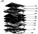
- FIG. 2 is an exploded perspective view of an antenna module according to an exemplary embodiment
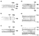
- FIG. 3 is a flowchart illustrating a method of manufacturing an antenna module according to an exemplary embodiment.
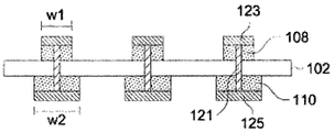
- FIG. 4 is a diagram illustrating a case in which a first pattern and a second pattern have different widths in an antenna module according to an exemplary embodiment.
- FIG 5 illustrates a first pattern in an antenna module according to an exemplary embodiment.
- FIG. 6 illustrates a second pattern in an antenna module according to an exemplary embodiment.
- FIG. 7 is a view illustrating a first NFC pattern formed on an upper surface of a magnetic sheet in an antenna module according to an exemplary embodiment.
- FIG. 8 illustrates a second NFC pattern formed on a bottom surface of a magnetic sheet in an antenna module according to an exemplary embodiment.
- FIG 9 illustrates a first MST pattern formed on an upper surface of a magnetic sheet in an antenna module according to an exemplary embodiment.
- FIG. 10 illustrates a second MST pattern formed on a bottom surface of a magnetic sheet in an antenna module according to an exemplary embodiment.
- FIG. 11 is a view illustrating a state in which an MST pattern and a WPC pattern are formed on an upper surface of a magnetic sheet according to an exemplary embodiment.
- FIG. 12 illustrates a first WPC pattern formed on an upper surface of a magnetic sheet in an antenna module according to an exemplary embodiment.
- FIG. 13 is a view illustrating a second WPC pattern formed on a bottom surface of a magnetic sheet in an antenna module according to an exemplary embodiment.
- FIG. 14 is a view illustrating a connection portion in an antenna module according to an exemplary embodiment.
- first and second may be used to describe various components, but the components should not be limited by the terms. The terms may be used for the purpose of distinguishing one component from another component.
- the first component may be referred to as the second component, and similarly, the second component may also be referred to as the first component.
- FIG. 2 is an exploded perspective view of an antenna module according to an exemplary embodiment.
- the antenna module 100 includes a magnetic sheet 102, a first bonding sheet 104, a second bonding sheet 106, a first pattern 108, a second pattern 110, and a first pattern.
- the cover sheet 112, the second cover sheet 114, and the heat diffusion sheet 116 may be included.
- the magnetic sheet 102 may be formed of a material having a property of magnetizing when a current flows through the first pattern 108 and the second pattern 110.
- the magnetic sheet 102 may include at least one of Ferrite, Nano Crystal, Amorphous, Permoloy, and Polymer Metal.
- the lower surface of the first bonding sheet 104 may be attached to the upper surface of the magnetic sheet 102.
- the first bonding sheet 104 serves to adhere the first pattern 108 to the upper surface of the magnetic sheet 102.
- the upper surface of the second bonding sheet 106 may be attached to the lower surface of the magnetic sheet 102.
- the second bonding sheet 106 serves to adhere the second pattern 110 to the bottom surface of the magnetic sheet 102.
- the first pattern 108 may be adhered to the top surface of the first bonding sheet 104.
- the first pattern 108 is directly bonded to the upper surface of the magnetic sheet 102 by the first bonding sheet 104.
- the first pattern 108 is an antenna pattern and may include a plurality of patterns of different frequency bands.
- the first pattern 108 may include a near field communication (NFC) pattern, a magnetic secure transmission (MST) pattern, and a wireless (WPC) pattern.
- NFC near field communication
- MST magnetic secure transmission
- WPC wireless
- Power Charge pattern may be included.
- the second pattern 110 may be attached to the bottom surface of the second bonding sheet 106.
- the second pattern 110 is directly adhered to the bottom surface of the magnetic sheet 102 by the second bonding sheet 106.
- the second pattern 110 is an antenna pattern and may include a plurality of patterns of different frequency bands.
- the second pattern 110 may include a Near Field Communication (NFC) pattern, a Magnetic Secure Transmission (MST) pattern, and a Wireless PCC.
- NFC Near Field Communication
- MST Magnetic Secure Transmission
- Wireless PCC Wireless PCC
- Power Charge pattern may be included.
- the antenna module 100 includes an NFC pattern, an MST pattern, and a WPC pattern, and the NFC pattern, the MST pattern, and the WPC pattern are bonded to the upper and lower surfaces of the magnetic sheet 102 by the bonding sheets 104 and 106. Each can be formed. Plating layers (not shown) may be formed on the first pattern 108 and the second pattern 110, respectively. In addition, the first pattern 108 and the second pattern 110 may be electrically connected to each other through a via hole (not shown) formed through the magnetic sheet 102.
- the first cover sheet 112 may be formed on the first pattern 108.
- the first cover sheet 112 serves to protect the first pattern 108 from the external environment.
- the first cover sheet 112 may cover the first pattern 108 while being bonded to the top surface of the first bonding sheet 104.
- the second cover sheet 114 may be formed under the second pattern 110.
- the second cover sheet 114 serves to protect the second pattern 110 from the external environment.
- the second cover sheet 114 may cover the second pattern 110 while being adhered to the bottom surface of the second bonding sheet 106.
- the heat diffusion sheet 116 may be formed on the first cover sheet 112.
- the heat diffusion sheet 116 may be attached to the first cover sheet 112 through the double-sided adhesive tape 117 at the top of the first cover sheet 112.
- the heat diffusion sheet 116 may serve to discharge heat generated from the antenna module 100 to the outside.
- the heat diffusion sheet 116 may be made of a material having excellent thermal conductivity (for example, graphite).
- the heat diffusion sheet 116 is described as being formed on the upper portion of the first cover sheet 112, but the present invention is not limited thereto, and the heat diffusion sheet 116 without the first cover sheet 112 may include the first pattern 108. ) May be formed covering.
- the heat diffusion sheet 116 may be formed under the second cover sheet 114 or may cover the second pattern 110 without the second cover sheet 114.
- the antenna module 100 may further include a carrier 118 formed under the second cover sheet 114.
- Carrier 118 may be used to handle antenna module 100.
- the carrier 118 may be formed with a contact reinforcement 119 for reinforcing the contact of the antenna pattern.
- the antenna pattern is formed on the flexible printed circuit board (FPCB) and not laminated with the magnetic sheet, the antenna pattern is formed directly on the magnetic sheet, thereby reducing the thickness of the antenna module.
- FPCB flexible printed circuit board
- the antenna pattern is formed directly on the magnetic sheet, thereby reducing the thickness of the antenna module.
- the process of laminating the FPCB and the magnetic sheet can be omitted, the entire manufacturing process of the antenna module can be simplified.
- FIG. 3 is a flowchart illustrating a method of manufacturing an antenna module according to an exemplary embodiment.
- the first metal thin film 108a and the second metal thin film 110a are formed on the upper and lower surfaces of the magnetic sheet 102, respectively (FIG. 3A). Specifically, the first metal thin film 108a is adhered to the upper surface of the magnetic sheet 102 through the first bonding sheet 104, and the second bonding sheet 106 is attached to the lower surface of the magnetic sheet 102.
- the metal thin film 110a may be bonded. In this case, one end portions of the first metal thin film 108a and the second metal thin film 110a may be bonded to extend outward from the edge of the magnetic sheet 102. Connection terminals may be formed in portions extending from the first metal thin film 108a and the second metal thin film 110a to the outside of the magnetic sheet 102, respectively.
- a via hole 121 that electrically connects the first metal thin film 108a and the second metal thin film 110a is formed (FIG. 3B).
- a through hole penetrates the first metal thin film 108a, the magnetic sheet 102, and the second metal thin film 110a to a portion where the first metal thin film 108a and the second metal thin film 110a are electrically connected.
- the via hole 121 may be formed by filling the inside of the through hole with a conductive material. In this case, the inner wall of the through hole may be plated to electrically connect the first metal thin film 108a and the second metal thin film 110a.
- first metal thin film 108a and the second metal thin film 110a are etched to form the first pattern 108 and the second pattern 110 on the top and bottom surfaces of the magnetic sheet 102, respectively.
- first pattern 108 and the second pattern 110 are not shown in a pattern form but shown in a thin film form.
- the first pattern 108 and the second pattern 110 may be formed through a photolithography process.
- the first pattern 108 and the second pattern 110 may be formed to include an NFC pattern, an MST pattern, and a WPC pattern, respectively. Widths and thicknesses of the first pattern 108 and the second pattern 110 may be the same.
- the present invention is not limited thereto, and at least one of the width and thickness of the first pattern 108 and the second pattern 110 may be formed differently.
- the magnetic sheet 102 also serves as a support member (eg, a substrate) for supporting the first pattern 108 and the second pattern 110.
- the first pattern 108 and the second pattern 110 are formed on the upper and lower surfaces of the magnetic sheet 102, respectively, and are electrically connected by the via holes 121. Since each connection terminal formed in the portion extending outward of the magnetic sheet 102 of the two patterns 110 does not contact each other, electrical short can be prevented.
- the first plating layer 123 is formed on the top surface of the first pattern 108, and the second plating layer 125 is formed on the bottom surface of the second pattern 110 (FIG. 3D).
- the first plating layer 123 and the second plating layer 125 may be formed with the same thickness or may be formed with a different thickness as necessary.
- the first plating layer 123 may be formed thicker than the second plating layer 125.
- the overall thickness of the first pattern portion that is, the first pattern 108 and the first plating layer 123) is thickened to increase radiation efficiency or wireless charging efficiency.
- the thickness of the second plating layer 125 As the thickness of the second plating layer 125 is adjusted, the thickness of the first pattern portion and the second pattern portion (that is, the second pattern 110 and the second plating layer 125) may be adjusted as necessary.
- the first cover sheet 112 is formed on the upper portion of the first pattern 108 to form the first cover sheet 112, and the second pattern 110 is covered on the lower portion of the second pattern 110.
- the second cover sheet 114 is formed (FIG. 3E). Specifically, the first cover sheet 112 is positioned on the upper portion of the first pattern 108, the second cover sheet 114 is positioned on the lower portion of the second pattern 110, and then a hot press process is performed.
- the first cover sheet 112 may be formed on the first pattern 108, and the second cover sheet 114 may be formed on the lower portion of the second pattern 110.
- the heat diffusion sheet 116 is formed on the first cover sheet 112 (FIG. 3F).
- the heat diffusion sheet 116 may be attached to the upper portion of the first cover sheet 112 using a double-sided tape or the like.
- FIG. 4 is a diagram illustrating a case in which a first pattern and a second pattern have different widths in an antenna module according to an exemplary embodiment.
- the bonding sheets 104 and 106 are omitted for convenience of description.
- This can be formed widely.
- the width of the pattern is formed wide, the cross-sectional area of the circuit can be widened to reduce the resistance, thereby improving the efficiency of the entire circuit.
- the first plating layer 123 and the second plating layer 125 may be formed to have the same width as that of the first pattern 108 and the second pattern 110, respectively.
- the width w2 of the second pattern 110 is formed to be wider than the width w1 of the first pattern 108
- the width w1 of the first pattern 108 is not limited thereto. It may be formed to be wider than the width w2 of the second pattern 110.
- the thickness of the first pattern 108 and the thickness of the second pattern 110 are shown to be the same, the thickness of the first pattern 108 and the thickness of the second pattern 110 are not limited thereto. It may be formed differently.
- the first pattern 108 and the second pattern 110 may be formed to include at least one of an NFC pattern, an MST pattern, and a WPC pattern, respectively.
- the first pattern 108 and the second pattern 110 of the antenna module 100 will be described in detail.
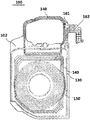
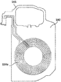
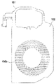
- FIG. 5 is a diagram illustrating a first pattern 108 in an antenna module according to an exemplary embodiment
- FIG. 6 is a diagram illustrating a second pattern 110 in an antenna module according to an exemplary embodiment. That is, FIG. 5 illustrates a first pattern 108 formed on the upper surface of the magnetic sheet 102, and FIG. 6 illustrates a second pattern 110 formed on the lower surface of the magnetic sheet 102.
- the first pattern 108 and the second pattern 110 may include an NFC pattern 130, an MST pattern 140, and a WPC pattern 150, respectively.
- the NFC pattern 130, the MST pattern 140, and the WPC pattern 150 may be formed to be spaced apart from each other in order from the outside of the magnetic sheet 102. That is, the WPC pattern 150 is formed at the center of the magnetic sheet 102, the MST pattern 140 is formed outside the WPC pattern 150, and the NFC pattern 130 is formed outside the MST pattern 140. Can be formed.
- the magnetic sheet 102 may be formed in a substantially rectangular shape.
- the present invention is not limited thereto and may be changed in various forms according to the internal structure of the portable terminal in which the antenna module 100 is mounted.
- the magnetic sheet 102 may be formed with an extension 161 on one side (the upper side in FIGS. 5 and 6) of the magnetic sheet 102.
- the extension part 161 may extend from one side (left side) and the other side (right side) of the upper side of the magnetic sheet 102, and each extended part may be connected to each other.
- a hole may be formed inside the extension part 161 according to the internal structure of the portable terminal.
- the extension part 161 may be formed in a semicircular arc (or half loop) shape on the upper side of the magnetic sheet 102.
- One side of the extension portion 161 may be formed with a connection portion 162, the connection terminal of the NFC pattern 130, MST pattern 140, and the WPC pattern 150 is formed.
- the magnetic sheet 102 may be formed with a thermistor 165 capable of measuring the temperature of at least one of the NFC pattern 130, the MST pattern 140, and the WPC pattern 150.
- a thermistor 165 capable of measuring the temperature of at least one of the NFC pattern 130, the MST pattern 140, and the WPC pattern 150.
- the current supply to the pattern may be cut off.
- the thermistor 165 is shown as being formed on the upper side of the magnetic sheet 102, but is not limited thereto, and the forming position of the thermistor 165 may be variously changed as necessary.
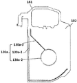
- FIG. 7 is a view illustrating a first NFC pattern 130a formed on an upper surface of a magnetic sheet 102 in an antenna module according to an exemplary embodiment
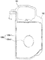
- FIG. 8 illustrates a magnetic sheet 102 in an antenna module according to an exemplary embodiment. Is a view showing the second NFC pattern 130b formed on the bottom surface.
- the first NFC pattern 130a may be formed along one side edge of the magnetic sheet 102 (for example, the left edge) and the lower edge of the magnetic sheet 102.
- the second NFC pattern 130b is spaced apart from the 2-1 NFC pattern 130b-1 and the 2-1 NFC pattern 130b-1 formed along each edge of the magnetic sheet 102, and the magnetic sheet 102. It may include a second-2 NFC pattern (130b-2) formed in a circular shape in the center portion.
- the second-2 NFC pattern 130b-2 may be formed to correspond to the first-2 NFC pattern 130a-2.
- a part of the first-first NFC pattern 130a-1 and the second-first NFC pattern 130b-1 formed on the lower edge of the magnetic sheet 102 is bent in accordance with the shape of the magnetic sheet 102. Can be formed.
- the first NFC pattern 130a and the second NFC pattern 130b may be electrically connected through a via hole.
- NFC performance can be further improved. That is, the 1-2 NFC pattern 130a-2 and the 2-2 NFC pattern 130b-2 are formed to be spaced apart from the WPC pattern 150 inside the WPC pattern 150 which will be described later. 130 may be extended to further improve NFC performance.
- the NFC pattern 130 is illustrated as being a conductive line of one turn, but this is merely an example for convenience of understanding and may be formed of a plurality of conductive lines. Of course.
- the first component may be referred to as a second component, and the second component may also be referred to as the second component. Can be named one component.
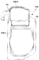
- FIG. 9 illustrates a first MST pattern 140a formed on an upper surface of the magnetic sheet 102 in the antenna module according to an exemplary embodiment
- FIG. 10 illustrates the magnetic sheet 102 in the antenna module according to an exemplary embodiment. Is a view showing the second MST pattern 140b formed on the lower surface of the substrate.
- the first MST pattern 140a is formed at a distance from the edge of the magnetic sheet 102 and is formed in a loop shape, and the first-first MST pattern 140a-1 and the magnetic sheet are formed in a loop shape.
- the first and second MST patterns 140a-2 formed in a loop shape on the upper side and the extension part 161 of the 102 may be included.
- the first-first MST patterns 140a-1 may be formed to be spaced apart from each other inside the first-first NFC pattern 130a-1.
- the 1-2 MST pattern 140a-2 may be formed to extend from the 1-1 MST pattern 140a-1, but is not limited thereto and is spaced apart from the 1-1 MST pattern 140a-1. It may be provided to be coupled to the first-first MST pattern 140a-1.
- the second MST pattern 140b is formed at a distance from the edge of the magnetic sheet 102 and is formed in a loop shape, and the upper and extension portions of the second-1 MST pattern 140b-1 and the magnetic sheet 102 ( 161 may include the 2-2 MST pattern 140b-2 formed in a loop shape.
- the 2-1 MST pattern 140b-1 may be formed to be spaced apart from each other inside the 2-1 NFC pattern 130b-1.
- the 2-2 MST pattern 140b-2 may be formed to extend from the 2-1 MST pattern 140b-1, but is not limited thereto and is spaced apart from the 2-1 MST pattern 140b-1. It may be provided to be coupled to the 2-1 MST pattern 140b-1.
- the first MST pattern 140a and the second MST pattern 140b may be electrically connected through the via hole.
- the inner length in the horizontal direction of the 1-1 MST pattern 140a-1 and the 2-1 MST pattern 140b-1 formed in a loop shape may be formed to be equal to or less than the diameter of the WPC pattern 150 to be described later. have.
- the longitudinal inner lengths of the 1-1 MST pattern 140a-1 and the 2-1 MST pattern 140b-1 may be formed to be equal to or greater than the diameter of the WPC pattern 150 to be described later.
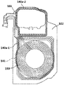
- FIG. 11 illustrates a state in which an MST pattern 140 (more specifically, a first MST pattern 140a) and a WPC pattern 150 are formed on an upper surface of the magnetic sheet 102 according to an exemplary embodiment.
- MST pattern 140 more specifically, a first MST pattern 140a
- WPC pattern 150 are formed on an upper surface of the magnetic sheet 102 according to an exemplary embodiment.
- the upper surface of the magnetic sheet 102 is shown for convenience of description, but the patterns formed on the lower surface of the magnetic sheet 102 may be understood in the same manner.
- the 1-1 MST pattern 140a-1 is formed.
- the first-first MST pattern 140a-1 may include a curved portion 141 that is bent outward in the vertical direction. As such, by forming the bent portion 141 in the 1-1 MST pattern 140a-1, the length of the 1-1 MST pattern 140a-1 is prevented from overlapping the WPC pattern 150 while being the length corresponding to the bend. The effect of extending the pattern length can be obtained.
- by arranging a plurality of antenna patterns in the magnetic sheet 102 of a predetermined size it is possible to increase the space utilization.
- the inner length of the first-first MST pattern 140a-1 in the longitudinal direction is illustrated as being greater than or equal to the diameter of the WPC pattern 150, the present invention is not limited thereto and the length of the first-first MST pattern 140a-1 is not limited thereto.
- the inner length of the may also be formed to be less than the diameter of the WPC pattern 150.
- the bent portion 141 may be formed in the horizontal direction of the 1-1 MST pattern 140a-1 so as not to overlap the WPC pattern 150.
- the bent portion 141 is formed in each of the horizontal direction and the vertical direction of the 1-1 MST pattern 140a-1 to prevent the overlapping of the WPC pattern 150 within the predetermined size of the magnetic sheet 102 while corresponding frequency bands. It is possible to obtain the electrical length value required for.
- the MST pattern 140 is for the replacement of the credit card, when the payment through the portable terminal mounted antenna module 100, the direction of approaching the portable terminal to the point of sales (POS) terminal for each user Can be different.
- POS point of sales
- one user may approach the POS terminal with the portable terminal in a horizontal direction, while another user may approach the POS terminal with the top or bottom of the portable terminal tilted.
- the direction of approaching the mobile terminal to the POS terminal may be different for each payment, if the payment is to be performed when the portable terminal is approached to the POS terminal in a specific direction, the user may feel uncomfortable. What is needed is a way to make payments regardless of the direction of approach.
- the MST pattern 140 is also formed in the extension part 161 (that is, the MST pattern 140 is formed in the first-second MST pattern 140a-2 and the second-second MST pattern 140b. -2)), the payment can be made using the MST pattern 140 regardless of the approaching direction of the portable terminal.
- the MST pattern 140 is also formed in the extension part 161 formed by extending from one side of the magnetic sheet 102 (in other words, the MST pattern 140 is formed in the entire area of the portable terminal, not a partial area of the portable terminal.
- the MST pattern 140 is also formed in the extension part 161 formed by extending from one side of the magnetic sheet 102 (in other words, the MST pattern 140 is formed in the entire area of the portable terminal, not a partial area of the portable terminal.
- payment can be made using the MST pattern 140 in each direction.
- FIG. 12 illustrates a first WPC pattern 150a formed on an upper surface of the magnetic sheet 102 in the antenna module according to an exemplary embodiment
- FIG. 13 illustrates the magnetic sheet 102 in the antenna module according to an exemplary embodiment. Is a view showing the second WPC pattern 150b formed on the lower surface of the panel.
- the first WPC pattern 150a and the second WPC pattern 150b may each have a circular shape at the center of the magnetic sheet 102.
- the first WPC pattern 150a and the second WPC pattern 150b may have a maximum number of turns in the magnetic sheet 102 having a predetermined size because the wireless charging efficiency increases as the number of turns increases.
- the first WPC pattern 150a and the second WPC pattern 150b may be electrically connected through the via holes.
- connection unit 14 is a diagram illustrating a connection unit in an antenna module according to an exemplary embodiment.
- a connection part 162 may be formed at one side of the extension part 161.
- a first connection terminal 171, a second connection terminal 173, a third connection terminal 175, and a fourth connection terminal 177 may be formed.
- the first connection terminal 171 may be electrically connected to the NFC pattern 130.
- the second connection terminal 173 may be electrically connected to the MST pattern 140.
- the third connection terminal 175 may be electrically connected to the WPC pattern 150.
- the fourth connection terminal 177 may be electrically connected to the thermistor 165.
Landscapes
- Engineering & Computer Science (AREA)
- Power Engineering (AREA)
- Computer Networks & Wireless Communication (AREA)
- Signal Processing (AREA)
- Details Of Aerials (AREA)
- Telephone Set Structure (AREA)
Abstract
L'invention porte sur un module d'antenne, sur son procédé de fabrication et sur un terminal mobile le comprenant. Le module d'antenne selon un exemple de mode de réalisation comprend : une feuille magnétique; un premier motif formé sur une surface de la feuille magnétique; une première feuille de couverture formée pour recouvrir le premier motif sur ladite surface de la feuille magnétique; un second motif formé sur l'autre surface de la feuille magnétique; une seconde feuille de couverture formée pour recouvrir le second motif sur l'autre surface de la feuille magnétique; et au moins un trou d'interconnexion, formé à travers le premier motif, la feuille magnétique et le second motif, pour connecter électriquement le premier motif au second motif.
Applications Claiming Priority (2)
| Application Number | Priority Date | Filing Date | Title |
|---|---|---|---|
| KR1020160061701A KR20170130889A (ko) | 2016-05-19 | 2016-05-19 | 안테나 모듈과 그 제조 방법 및 이를 구비한 휴대용 단말기 |
| KR10-2016-0061701 | 2016-05-19 |
Publications (1)
| Publication Number | Publication Date |
|---|---|
| WO2017200236A1 true WO2017200236A1 (fr) | 2017-11-23 |
Family
ID=60325990
Family Applications (1)
| Application Number | Title | Priority Date | Filing Date |
|---|---|---|---|
| PCT/KR2017/004852 Ceased WO2017200236A1 (fr) | 2016-05-19 | 2017-05-11 | Module d'antenne, son procédé de fabrication, et terminal mobile le comprenant |
Country Status (2)
| Country | Link |
|---|---|
| KR (1) | KR20170130889A (fr) |
| WO (1) | WO2017200236A1 (fr) |
Cited By (2)
| Publication number | Priority date | Publication date | Assignee | Title |
|---|---|---|---|---|
| CN110299607A (zh) * | 2018-03-23 | 2019-10-01 | 三星电机株式会社 | 天线模块和包括天线模块的电子装置 |
| US11728564B2 (en) | 2019-11-27 | 2023-08-15 | AQ Corporation | Smartphone antenna in flexible PCB |
Families Citing this family (4)
| Publication number | Priority date | Publication date | Assignee | Title |
|---|---|---|---|---|
| KR101872399B1 (ko) | 2017-12-29 | 2018-06-28 | 에이큐 주식회사 | 인서트 구조를 갖는 콤보 안테나 |
| KR101883109B1 (ko) * | 2017-07-20 | 2018-07-27 | 삼성전기주식회사 | 안테나 모듈 |
| KR101897511B1 (ko) | 2018-05-23 | 2018-09-12 | 에이큐 주식회사 | 인서트 구조를 갖는 콤보 안테나 |
| KR102694433B1 (ko) * | 2019-04-26 | 2024-08-13 | 주식회사 아모센스 | 안테나 모듈 및 이를 구비한 휴대 단말 커버 |
Citations (5)
| Publication number | Priority date | Publication date | Assignee | Title |
|---|---|---|---|---|
| KR101197684B1 (ko) * | 2009-04-07 | 2012-11-05 | 주식회사 아모텍 | 자성시트, 자성시트와 일체화된 방사체 패턴을 구비한 무선 식별 안테나 및 그 제조방법 |
| KR101381135B1 (ko) * | 2013-01-15 | 2014-04-04 | 김선기 | 연성회로기판 및 이를 적용한 이동통신기기용 내장형 안테나 |
| JP2015149405A (ja) * | 2014-02-06 | 2015-08-20 | デクセリアルズ株式会社 | アンテナ装置、非接触電力伝送用アンテナユニット、及び電子機器 |
| KR101554129B1 (ko) * | 2015-01-23 | 2015-09-21 | 주식회사 아이엠텍 | 무선통신용 플렉시블 회로기판 |
| KR20150131925A (ko) * | 2014-05-15 | 2015-11-25 | 주식회사 아이티엠반도체 | Nfc 통신이 가능한 전자장치 |
-
2016
- 2016-05-19 KR KR1020160061701A patent/KR20170130889A/ko not_active Ceased
-
2017
- 2017-05-11 WO PCT/KR2017/004852 patent/WO2017200236A1/fr not_active Ceased
Patent Citations (5)
| Publication number | Priority date | Publication date | Assignee | Title |
|---|---|---|---|---|
| KR101197684B1 (ko) * | 2009-04-07 | 2012-11-05 | 주식회사 아모텍 | 자성시트, 자성시트와 일체화된 방사체 패턴을 구비한 무선 식별 안테나 및 그 제조방법 |
| KR101381135B1 (ko) * | 2013-01-15 | 2014-04-04 | 김선기 | 연성회로기판 및 이를 적용한 이동통신기기용 내장형 안테나 |
| JP2015149405A (ja) * | 2014-02-06 | 2015-08-20 | デクセリアルズ株式会社 | アンテナ装置、非接触電力伝送用アンテナユニット、及び電子機器 |
| KR20150131925A (ko) * | 2014-05-15 | 2015-11-25 | 주식회사 아이티엠반도체 | Nfc 통신이 가능한 전자장치 |
| KR101554129B1 (ko) * | 2015-01-23 | 2015-09-21 | 주식회사 아이엠텍 | 무선통신용 플렉시블 회로기판 |
Cited By (4)
| Publication number | Priority date | Publication date | Assignee | Title |
|---|---|---|---|---|
| CN110299607A (zh) * | 2018-03-23 | 2019-10-01 | 三星电机株式会社 | 天线模块和包括天线模块的电子装置 |
| US11728564B2 (en) | 2019-11-27 | 2023-08-15 | AQ Corporation | Smartphone antenna in flexible PCB |
| US12003018B2 (en) | 2019-11-27 | 2024-06-04 | AQ Corporation | Smartphone with wireless power charing antenna |
| US12278421B2 (en) | 2019-11-27 | 2025-04-15 | AQ Corporation | Smartphone with wireless power charging antenna |
Also Published As
| Publication number | Publication date |
|---|---|
| KR20170130889A (ko) | 2017-11-29 |
Similar Documents
| Publication | Publication Date | Title |
|---|---|---|
| WO2017200236A1 (fr) | Module d'antenne, son procédé de fabrication, et terminal mobile le comprenant | |
| KR101179398B1 (ko) | 무접점 전력 전송 장치 및 이를 구비하는 전자 기기 | |
| WO2017007231A1 (fr) | Antenne sans fil pour charge sans fil et communication nfc et terminal sans fil auquel celle-ci est appliquée | |
| EP2518904B1 (fr) | Dispositif de transmission de puissance sans contact | |
| WO2016186443A1 (fr) | Unité d'antenne combo et module de réception d'énergie sans fil la comprenant | |
| WO2017074104A1 (fr) | Feuille de blindage de champ magnétique destinée à la transmission d'énergie sans fil et module de réception d'énergie sans fil comprenant cette dernière | |
| WO2017078481A1 (fr) | Module d'antenne du type à combinaison | |
| WO2016159551A1 (fr) | Unité de dissipation de chaleur pour charge sans fil et module de charge électrique sans fil la comportant | |
| WO2017135687A1 (fr) | Unité de blindage pour module d'émission d'énergie sans fil, et module d'émission d'énergie sans fil la comprenant | |
| WO2016114528A1 (fr) | Unité de rayonnement de chaleur et dispositif d'envoi et de réception d'énergie sans fil la comprenant | |
| WO2016072779A1 (fr) | Émetteur pour chargeur sans fil | |
| WO2016190649A1 (fr) | Module de réception de puissance sans fil | |
| WO2017048062A1 (fr) | Module d'antenne de communication en champ proche et terminal mobile pourvu dudit module | |
| CN208423162U (zh) | 天线模块及电子设备 | |
| WO2016186444A1 (fr) | Unité de blindage pour charge sans fil et module de transmission d'énergie sans fil la comprenant | |
| WO2017023080A1 (fr) | Module de transfert de puissance sans fil pour véhicules | |
| WO2017069581A1 (fr) | Module d'antenne de véhicule | |
| WO2017119773A1 (fr) | Module d'antenne empilé | |
| WO2017142350A1 (fr) | Coque arrière de terminal portable et module d'antenne intégré à une coque arrière comprenant cette dernière | |
| WO2019151693A1 (fr) | Récepteur de charge sans fil permettant d'améliorer les performances d'une antenne | |
| CN105247732A (zh) | Nfc天线模块及由其组成的携带终端 | |
| WO2021221361A1 (fr) | Module d'antenne et dispositif de communication sans fil le comprenant | |
| EP3649698A1 (fr) | Boîtier de dispositif électronique et dispositif électronique | |
| US10698455B2 (en) | Antenna module and electronic device including the same | |
| WO2017175886A1 (fr) | Structure d'antenne |
Legal Events
| Date | Code | Title | Description |
|---|---|---|---|
| NENP | Non-entry into the national phase |
Ref country code: DE |
|
| 121 | Ep: the epo has been informed by wipo that ep was designated in this application |
Ref document number: 17799594 Country of ref document: EP Kind code of ref document: A1 |
|
| 122 | Ep: pct application non-entry in european phase |
Ref document number: 17799594 Country of ref document: EP Kind code of ref document: A1 |