WO2017203661A1 - Dispositif d'imagerie holographique numérique - Google Patents
Dispositif d'imagerie holographique numérique Download PDFInfo
- Publication number
- WO2017203661A1 WO2017203661A1 PCT/JP2016/065614 JP2016065614W WO2017203661A1 WO 2017203661 A1 WO2017203661 A1 WO 2017203661A1 JP 2016065614 W JP2016065614 W JP 2016065614W WO 2017203661 A1 WO2017203661 A1 WO 2017203661A1
- Authority
- WO
- WIPO (PCT)
- Prior art keywords
- imaging device
- light
- photoelectric conversion
- incident angle
- digital holographic
- Prior art date
- Legal status (The legal status is an assumption and is not a legal conclusion. Google has not performed a legal analysis and makes no representation as to the accuracy of the status listed.)
- Ceased
Links
Images


Classifications
-
- G—PHYSICS
- G03—PHOTOGRAPHY; CINEMATOGRAPHY; ANALOGOUS TECHNIQUES USING WAVES OTHER THAN OPTICAL WAVES; ELECTROGRAPHY; HOLOGRAPHY
- G03H—HOLOGRAPHIC PROCESSES OR APPARATUS
- G03H1/00—Holographic processes or apparatus using light, infrared or ultraviolet waves for obtaining holograms or for obtaining an image from them; Details peculiar thereto
- G03H1/04—Processes or apparatus for producing holograms
- G03H1/0443—Digital holography, i.e. recording holograms with digital recording means
-
- G—PHYSICS
- G02—OPTICS
- G02B—OPTICAL ELEMENTS, SYSTEMS OR APPARATUS
- G02B21/00—Microscopes
-
- G—PHYSICS
- G02—OPTICS
- G02B—OPTICAL ELEMENTS, SYSTEMS OR APPARATUS
- G02B21/00—Microscopes
- G02B21/0004—Microscopes specially adapted for specific applications
- G02B21/0008—Microscopes having a simple construction, e.g. portable microscopes
-
- G—PHYSICS
- G03—PHOTOGRAPHY; CINEMATOGRAPHY; ANALOGOUS TECHNIQUES USING WAVES OTHER THAN OPTICAL WAVES; ELECTROGRAPHY; HOLOGRAPHY
- G03H—HOLOGRAPHIC PROCESSES OR APPARATUS
- G03H1/00—Holographic processes or apparatus using light, infrared or ultraviolet waves for obtaining holograms or for obtaining an image from them; Details peculiar thereto
- G03H1/04—Processes or apparatus for producing holograms
- G03H1/0402—Recording geometries or arrangements
- G03H1/041—Optical element in the object space affecting the object beam, not otherwise provided for
-
- G—PHYSICS
- G03—PHOTOGRAPHY; CINEMATOGRAPHY; ANALOGOUS TECHNIQUES USING WAVES OTHER THAN OPTICAL WAVES; ELECTROGRAPHY; HOLOGRAPHY
- G03H—HOLOGRAPHIC PROCESSES OR APPARATUS
- G03H1/00—Holographic processes or apparatus using light, infrared or ultraviolet waves for obtaining holograms or for obtaining an image from them; Details peculiar thereto
- G03H1/04—Processes or apparatus for producing holograms
- G03H1/0486—Improving or monitoring the quality of the record, e.g. by compensating distortions, aberrations
-
- G—PHYSICS
- G03—PHOTOGRAPHY; CINEMATOGRAPHY; ANALOGOUS TECHNIQUES USING WAVES OTHER THAN OPTICAL WAVES; ELECTROGRAPHY; HOLOGRAPHY
- G03H—HOLOGRAPHIC PROCESSES OR APPARATUS
- G03H1/00—Holographic processes or apparatus using light, infrared or ultraviolet waves for obtaining holograms or for obtaining an image from them; Details peculiar thereto
- G03H1/04—Processes or apparatus for producing holograms
- G03H1/08—Synthesising holograms, i.e. holograms synthesized from objects or objects from holograms
- G03H1/0866—Digital holographic imaging, i.e. synthesizing holobjects from holograms
-
- G—PHYSICS
- G03—PHOTOGRAPHY; CINEMATOGRAPHY; ANALOGOUS TECHNIQUES USING WAVES OTHER THAN OPTICAL WAVES; ELECTROGRAPHY; HOLOGRAPHY
- G03H—HOLOGRAPHIC PROCESSES OR APPARATUS
- G03H1/00—Holographic processes or apparatus using light, infrared or ultraviolet waves for obtaining holograms or for obtaining an image from them; Details peculiar thereto
- G03H1/04—Processes or apparatus for producing holograms
- G03H1/0402—Recording geometries or arrangements
- G03H2001/0428—Image holography, i.e. an image of the object or holobject is recorded
-
- G—PHYSICS
- G03—PHOTOGRAPHY; CINEMATOGRAPHY; ANALOGOUS TECHNIQUES USING WAVES OTHER THAN OPTICAL WAVES; ELECTROGRAPHY; HOLOGRAPHY
- G03H—HOLOGRAPHIC PROCESSES OR APPARATUS
- G03H1/00—Holographic processes or apparatus using light, infrared or ultraviolet waves for obtaining holograms or for obtaining an image from them; Details peculiar thereto
- G03H1/04—Processes or apparatus for producing holograms
- G03H1/0443—Digital holography, i.e. recording holograms with digital recording means
- G03H2001/0447—In-line recording arrangement
-
- G—PHYSICS
- G03—PHOTOGRAPHY; CINEMATOGRAPHY; ANALOGOUS TECHNIQUES USING WAVES OTHER THAN OPTICAL WAVES; ELECTROGRAPHY; HOLOGRAPHY
- G03H—HOLOGRAPHIC PROCESSES OR APPARATUS
- G03H1/00—Holographic processes or apparatus using light, infrared or ultraviolet waves for obtaining holograms or for obtaining an image from them; Details peculiar thereto
- G03H1/04—Processes or apparatus for producing holograms
- G03H1/0443—Digital holography, i.e. recording holograms with digital recording means
- G03H2001/0452—Digital holography, i.e. recording holograms with digital recording means arranged to record an image of the object
-
- G—PHYSICS
- G03—PHOTOGRAPHY; CINEMATOGRAPHY; ANALOGOUS TECHNIQUES USING WAVES OTHER THAN OPTICAL WAVES; ELECTROGRAPHY; HOLOGRAPHY
- G03H—HOLOGRAPHIC PROCESSES OR APPARATUS
- G03H2223/00—Optical components
- G03H2223/50—Particular location or purpose of optical element
- G03H2223/53—Filtering the hologram information, i.e. the fringe pattern
Definitions
- the present invention relates to digital holographic imaging devices.
- a lens-free digital holographic imaging device In order to capture phase distribution information and intensity distribution information of a cell sample or the like, a lens-free digital holographic imaging device is used (see, for example, Patent Document 1).
- the digital holographic imaging apparatus irradiates illumination light onto the subject, measures the interference pattern obtained as a result by the imaging device, and re-executes phase distribution information or intensity distribution information of the subject by arithmetic processing from the interference pattern. Reconstruct.
- the present invention has been made in such a situation, and one of the exemplary objects of an aspect of the present invention is to provide a digital holographic imaging device in which spurious signals are suppressed.
- the digital holographic imaging apparatus includes an illumination unit that illuminates the test object with illumination light, and a plurality of pixels arranged in a two-dimensional manner on the photoelectric conversion surface, and an interference pattern formed by the illumination light that interacts with the test object And a limiting unit for limiting at least one of the spatial frequency of the interference pattern formed on the photoelectric conversion surface and the incident angle of light incident on the photoelectric conversion surface.
- the digital holographic imaging apparatus includes an illumination unit that illuminates the test object with illumination light, and a plurality of pixels arranged in a two-dimensional manner on the photoelectric conversion surface, and an interference pattern formed by the illumination light that interacts with the test object Photoelectric conversion so as to remove false signals from the image reconstructed based on the image data captured by the imaging device, provided between the imaging device for imaging the intensity distribution of the image, the photoelectric conversion surface and the test object And a limiting unit that acts on light incident on the surface.
- false signals can be suppressed and the image quality can be improved.
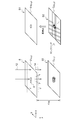
- FIG. 1 is a diagram showing a digital holographic imaging device according to a first embodiment. It is a figure which shows the digital holographic imaging device concerning 2nd Example.
- FIGS. 1 is a diagram showing a digital holographic imaging device according to a first embodiment. It is a figure which shows the digital holographic imaging device concerning 2nd Example.
- FIGS. 1 is a diagram showing a digital holographic imaging device according to a first embodiment. It is a figure which shows the digital holographic imaging device concerning 2nd Example.
- FIGS. 1 is a diagram showing a digital holographic imaging device according to a first embodiment. It is a figure which shows the digital holographic imaging device concerning 2nd Example.
- FIGS. 1 is a diagram showing a digital holographic imaging device according to a first embodiment. It is a figure which shows the digital holographic imaging device concerning 2nd Example.
- FIGS. 1 is a diagram showing a digital holographic imaging device according to a first embodiment. It is a figure which
- FIGS. 9A to 9C are diagrams for explaining the relationship between the interference pattern and the spatial frequency. It is a figure which illustrates the effect
- FIG. 11 (a) is a view showing a digital holographic imaging apparatus according to a first modification of the second embodiment, and FIG. 11 (b) is an incident angle in the digital holographic imaging apparatus of FIG. 11 (a) It is a figure which shows the characteristic of a restriction
- FIG.12 (a) is a figure which shows the digital holographic imaging device based on the 2nd modification of 2nd Example
- FIG.12 (b) is the incident angle in the digital holographic imaging device of Fig.12 (a). It is a figure which shows the characteristic of a restriction
- the digital holographic imaging apparatus includes an illumination unit that illuminates the test object with illumination light, and a plurality of pixels arranged in a two-dimensional manner on the photoelectric conversion surface, and an interference pattern formed by the illumination light that interacts with the test object And a limiting unit for limiting at least one of the spatial frequency of the interference pattern formed on the photoelectric conversion surface and the incident angle of light incident on the photoelectric conversion surface.
- the false signal can be removed or suppressed from the image representing the phase distribution or the intensity distribution of the test object reconstructed by the arithmetic processing from the image captured by the imaging device.
- the limiting unit may be provided between the test object and the photoelectric conversion surface.
- the high frequency component can be suitably suppressed and removed by causing the limiting portion to act on the light incident on the imaging device.
- the limiting unit may transmit spatial frequency components of 1 ⁇ 2 p or less. Thereby, false signals can be suitably removed and suppressed.
- the limiting unit may include an incident angle limiting unit that limits the incident angle of light incident on the photoelectric conversion surface.
- incident angle limiting unit limits the incident angle of light incident on the photoelectric conversion surface.
- the incident angle limiting unit may be formed inside the imaging device. Thereby, the incident angle can be limited at the position closest to the photoelectric conversion surface.
- the illumination light may be parallel light.
- the emission angle of the illumination light is ⁇ ill
- the wavelength is ⁇
- the pixel pitch of the imaging device is p
- the illumination light may be a spherical wave.
- the wavelength of the illumination light is ⁇
- the pixel pitch of the imaging device is p
- the distance between the photoelectric conversion surface and the exit surface of the illumination unit is z ill
- the distance between the photoelectric conversion surface and the sample surface where the test object is located is z obj
- ⁇ z ill / (z ill -z obj )
- the limiting unit may include an optical low pass filter.
- FIG. 1 is a diagram showing a basic configuration of a digital holographic imaging device 2 according to the embodiment.
- the dimensions (thickness, length, width, etc.) of each member described in the drawings may be scaled as appropriate for ease of understanding.
- the dimensions of a plurality of members do not necessarily represent the magnitude relationship between them, and even if one member A is drawn thicker (longer) than another member B in the drawing, the member A May be thinner (shorter) than the member B.
- the digital holographic imaging device 2 can be used to observe an object having characteristics of a phase object, an amplitude object, or both of them, but the observation object is not particularly limited.
- a phase object such as a cell is taken as an example of an observation target (the test object 4).
- the test object 4 is held at a predetermined position by the sample holder 6.
- the surface on which the test object 4 is located is referred to as a sample surface 8.
- the digital holographic imaging device 2 outputs a subject image S1 indicating the phase distribution of the test object 4.
- the digital holographic imaging device 2 includes an illumination unit 10, an imaging device 20, an arithmetic unit 30, a display device 40, and a restriction unit 50.
- the digital holographic imaging device 2 may be constituted essentially of a lens free optical system, but may have an optical system not shown if necessary.
- the illumination unit 10 irradiates the object 4 with illumination light 12 having coherence.
- the configuration of the illumination unit 10 is not particularly limited, and a semiconductor laser or an LED can be used.
- the illumination light 12 may be a plane wave or a spherical wave, but is shown as a plane wave in FIG. In the figure, a light ray is represented by a solid line, and a wavefront is represented by a dotted line.
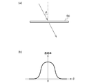
- FIG. 2 is a diagram for explaining the principle of the digital holographic imaging device 2.
- the test object 4 which is a phase object has a phase distribution ⁇ (x, y) in a first direction (x direction) of the sample surface 8 and a second direction (y direction) perpendicular thereto.
- the phase distribution ⁇ (x, y) corresponds to the shape, structure, composition, and the like of the test object 4, and the phase distribution ⁇ (x, y) is an observation target by the digital holographic imaging device 2.
- the illumination light 14 transmitted through the test subject 4 undergoes a phase shift according to the phase distribution ⁇ (x, y), and its wavefront is disturbed by the test subject 4.
- the illumination light 14 after being transmitted through the test object 4 includes light which is not subjected to the disturbance (diffraction) by the test object 4 and light which is diffracted by the test object 4 and they are separated by the distance z obj in the z direction. It propagates to form an interference pattern (also referred to as light intensity distribution) I (x, y) on the photoelectric conversion surface 22 of the imaging device 20.
- an interference pattern also referred to as light intensity distribution
- the imaging device 20 is a charge coupled device (CCD) or a complementary metal oxide semiconductor (CMOS) sensor, and includes a plurality of pixels arranged in a two-dimensional manner on the photoelectric conversion surface 22.
- the imaging device 20 captures an intensity distribution I (x, y) of an interference pattern formed by the illumination light 14 that has acted on the test object 4 and generates image data S2.
- imaging by the imaging device 20 is nothing but spatial sampling.
- the sampled (quantized) intensity distribution is denoted as I s (x, y).
- the image data S2 output from the imaging element 20 is input to the calculation unit 30.
- Arithmetic unit 30 reconstructs subject image S1 representing phase distribution ⁇ R (x, y) by arithmetic processing of intensity distribution I S (x, y) indicated by image data S2.
- the reconstructed phase distribution ⁇ R (x, y) corresponds to the phase distribution ⁇ (x, y) of the test object 4.
- Arithmetic unit 30 may be a combination of a general purpose computer and a software program, or may be a dedicated hardware. Since the arithmetic processing (algorithm) for reconstructing the subject image S1 from the image data S2 is known, the description will be omitted. For example, phase reconstruction methods including Fourier iteration can be used to reconstruct the subject image S1.
- the display device 40 displays the subject image S1 generated by the calculation unit 30.
- the display device 40 also has a function as a user interface of the digital holographic imaging device 2.
- the limiting unit 50 uses the photoelectric conversion surface 22 of the imaging device 20.
- the spatial frequency of the formed intensity distribution I (x, y) is limited, or (ii) the incident angle of light incident on the photoelectric conversion surface 22 is limited, or both of them are limited.
- the limitation part 50 is provided in the optical path of the illumination light 14, it is not limited to it.
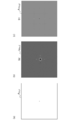
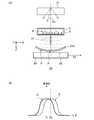
- FIGS. 3 (a) to 3 (c) are diagrams showing simulation results of the digital holographic imaging device 2 not provided with the limiting unit 50.
- FIG. Here, in order to simplify the explanation, an amplitude object is taken as an example.
- FIG. 3 (a) shows the amplitude distribution A (x, y) at the sample surface 8, where the transmittance inside the center radius of 5 microns is 0, and the transmittance in the other range is 1 .
- FIG. 3 (b) the light intensity distribution I (x, y) of the photoelectric conversion surface 22 of the image sensor 20, spatially sampled (ie captured) image data S2 obtained (i.e. the light intensity distribution I S ( x, y)).
- the light intensity distribution I (x, y) on the photoelectric conversion surface 22 causes the light having the amplitude distribution A of FIG. 3A to be Fresnel-propagated in the z direction with the distance between the photoelectric conversion surface 22 and the sample surface 8 being 1 mm.
- the light intensity distribution I (x, y) before sampling contains frequency components exceeding the Nyquist frequency fn, and the image data S2 obtained by sampling this, that is, the light intensity distribution I S (x, y) Aliasing (folding noise) occurs based on the sampling theorem.
- FIG. 3 (c) shows a subject image (amplitude distribution) S1 reconstructed from the image data S2 of FIG. 3 (b).
- the reconstructed subject image S1 can be calculated by Fresnel propagation of the image data S2 of FIG. 3B in the z direction by ⁇ 1 mm.
- the amplitude distribution A R (x, y) represented by the reconstructed subject image S 1 should ideally coincide with the amplitude distribution A (x, y) of FIG.
- the light intensity distribution I S (x, y) of the original image data S 2 includes aliasing noise, the influence spreads over the entire object image S 1 after reconstruction, and a real image (circle with radius 5 microns Regular false signals occur around). The above is the explanation of the false signal.
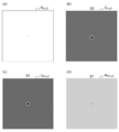
- FIGS. 4A to 4C are diagrams showing simulation results of the digital holographic imaging device 2 provided with the limiting unit 50.
- FIG. FIGS. 4A and 4B are similar to FIGS. 3A and 3B.
- FIG. 4C shows the light intensity distribution I S (x, y) obtained by spatially sampling the light intensity distribution I (x, y) of the photoelectric conversion surface 22 when the limiting unit 50 is effective.
- Image data S2 representing In this simulation, an optical low pass filter is used as the limiting unit 50.
- FIG. 4D shows a subject image S1 (amplitude distribution A R (x, y)) reconstructed from the image data S2 of FIG. 4C.
- the limiting unit 50 removes or attenuates spatial frequency components higher than the Nyquist frequency fn. By making the limiting unit 50 effective, high frequency components exceeding the Nyquist frequency fn included in the light intensity distribution I (x, y) of the photoelectric conversion surface 22 are reduced, and the light intensity distribution I (x, y) The aliasing noise included in the light intensity distribution I S (x, y) of FIG. 4C obtained by sampling is smaller than that of the image data S2 of FIG. 4B.
- the subject image S1 reconstructed from the image data S2 in which aliasing noise is suppressed is one in which a false signal is suppressed.
- FIGS. 5A and 5B are diagrams showing a subject (reconstructed) image S1 obtained when the restriction unit 50 is invalidated. As apparent from this comparison, by providing the limiting unit 50, it is possible to suppress false signals.
- narrowing the pixel pitch p while maintaining the same field of view means an increase in the number of pixels of the imaging device 20.
- the increase in the number of pixels explosively increases the amount of calculation when reconstructing the subject image S1 from the image data S2.
- the influence on the increase in computational complexity is particularly large when using phase recovery by iterative operation (for example, Fourier iteration) for reconstruction.
- suppression of false signals by the restriction unit 50 also has an advantage that an increase in the amount of computation can be suppressed.
- the object image S1 of FIG. 5 (b) is concentric with the coordinates (x 0 , y 0 ) not found in the object image S1 of FIG. There are streaks of Although it is thought that this fringe can be reduced by optimizing the low pass filter or using the limiting unit 50 other than the low pass filter, it may not be able to be completely removed, which may be undesirable. Therefore, the imaging mode in which the limiting unit 50 is enabled and the imaging mode in which the limiting unit 50 is disabled may be switched according to the test object 4.
- the above is the basic configuration of the digital holographic imaging device 2.
- the present invention extends to various devices that can be understood as FIG. 1 or derived from the above description, and is not limited to a particular configuration.
- FIG. 1 the basic configuration of the digital holographic imaging device 2.
- FIG. 6 is a view showing a digital holographic imaging device 2a according to the first embodiment.
- the calculation unit 30 and the display device 40 will be omitted.
- the limiting unit 50 includes the optical low pass filter 52 described above.
- the optical low pass filter 52 may use, for example, birefringence of a material such as quartz, or may use structural birefringence using a fine structure. If the light source of the illumination unit 10 is close to linearly polarized light, it is preferable to provide a wave plate in the illumination unit 10 and use circularly polarized light.
- the limiting unit 50 in the first embodiment limits the spatial frequency of the interference pattern (light intensity distribution I (x, y)) formed on the photoelectric conversion surface 22.
- the optical low pass filter 52 can be provided between the test object 4 and the photoelectric conversion surface 22.
- high frequency components included in the light intensity distribution in the surface on which the optical low pass filter 52 is located are removed.
- high frequency components exceeding the Nyquist frequency fn may appear.
- the optical low pass filter 52 is preferably disposed as close as possible to the photoelectric conversion surface 22.
- the optical low pass filter 52 may be formed integrally with the imaging device 20, for example.
- the optical low pass filter 52 and the imaging device 20 may be closely joined at a distance of zero.
- optical low pass filter 52 and the imaging device 20 are disposed separately, the space between them is filled with a sealing agent such as resin, and the above-described optical low pass filter 52 and the imaging device 20 are integrated. It is possible to suppress the occurrence of high frequency components generated due to adhesion of dust, generation of scratches, or similar factors.
- the height (thickness) of the device can be suppressed.
- FIG. 7 is a view showing a digital holographic imaging device 2b according to a second embodiment.
- the limiting unit 50 includes an incident angle limiting unit 54 that limits the incident angle of light incident on the photoelectric conversion surface 22.
- the incident angle limiting unit 54 is preferably provided in the vicinity of the photoelectric conversion surface 22.
- FIGS. 8A and 8B illustrate the incident angle limiting unit 54.
- FIG. FIG. 8A is a cross-sectional view of the incident angle limiting unit 54
- FIG. 8B is a diagram showing the incident angle dependency of the transmittance of the incident angle limiting unit 54.
- the incident angle limiting unit 54 can be manufactured, for example, by forming a dielectric multi-layered film on a substrate such as glass and adding incident angle dependency of the transmittance.
- the incident angle limiter 54 is preferably isotropically designed for polarization. Since the incident angle limiting unit 54 does not utilize birefringence, it has the advantage of being less subject to polarization restrictions than the optical low pass filter 52. If the characteristic of the incident angle limiting unit 54 has the dependency of the polarization direction, a polarizer may be added to make the illumination light 12 linearly polarized.
- the incident angle limiting unit 54 having the characteristic of FIG. 8B is disposed in parallel with the wavefront of the illumination light 12. Thereby, the incident angle limiting unit 54 transmits light which is not disturbed (diffracted) by the test object 4 and suppresses or removes the component having a large diffraction angle in the object light diffracted by the test object 4.
- FIGS. 9A to 9C are diagrams for explaining the relationship between the interference pattern and the spatial frequency.
- a wavefront perpendicular to the surface normal of the imaging device 20 is incident as the illumination light 12 will be considered for simplicity.
- the illumination light 12 is incident on the test object 4, and a part L1 of the illumination light 12 is incident on the imaging device 20 without being subjected to disturbance (diffraction) by the test object 4 as it is.
- Another part (object light) L ⁇ b> 2 is diffracted by the test object 4 and enters the imaging device 20. Interference between these two lights L1 and L2 causes interference fringes to be observed at the imaging device 20.
- the spatial frequency of the interference fringes observed on the imaging device 20 will be considered with reference to FIG.
- the pixel pitch of the imaging device 20 is p
- the period of the test object 4 that can be sampled correctly is in the range of P sig 22 p according to the Nyquist condition.
- NA is a numerical aperture
- FIG. 10 is a diagram schematically illustrating the operation of the incident angle limiting unit 54.
- Attention is focused on a certain point (observation point) X on the imaging device 20.
- Angles at which the observation point X is viewed from the three points P 1 , P 2 , and P 3 of the test object 4 are assumed to be ⁇ M1 , ⁇ M2 , and ⁇ M3 .
- Incident angle limiting unit 54 is to limit the incidence angle ⁇ of the image sensor 20, which means that for example removing incidence from the point P 3.
- the intensity of the photoelectric conversion surface 22 distribution I (x, y) can remove components P sig3 high spatial frequency point P 3 is formed.
- the incident angle limiter 54 can remove high spatial frequencies from the interference pattern, thus reducing the effects of aliasing.
- limiting the incident angle ⁇ of the light incident on the photoelectric conversion surface 22 by the incident angle limiting unit 54 corresponds to the space of the intensity distribution I (x, y) on the photoelectric conversion surface 22. It is equivalent to limiting the frequency.
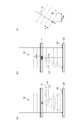
- FIG. 11A is a view showing a digital holographic imaging device 2c according to a first modification of the second embodiment.
- the wavefront of the illumination light 12 from the illumination unit 10 is inclined with respect to the sample surface 8 and the photoelectric conversion surface 22.
- the incident angle limiting unit 54 c is formed or arranged such that the surface normal is parallel to the light beam of the illumination light 12, that is, the surface normal is perpendicular to the wavefront of the illumination light 12. Therefore, in this modification, when the emission angle of the illumination light 12 is ⁇ ill , the incident angle limiting unit 54 c is disposed at the ⁇ ill inclination with respect to the photoelectric conversion surface 22.
- FIG. 11 (b) is a diagram showing the characteristics of the incident angle limiting unit 54c in the digital holographic imaging device 2c of FIG. 11 (a). ⁇ takes zero in the z-axis direction (vertical direction). By the incident angle restriction unit 54c is theta ill inclined having the characteristics of FIG. 8 (b), the transmission characteristic of the incident angle restriction unit 54c is shifted. Thereby, the incident angle limiting unit 54c transmits light which does not receive disturbance (diffraction) by the test object 4, and suppresses or removes the component having a large diffraction angle in the object light diffracted by the test object 4. be able to.
- limiting part 54 in case the illumination light 12 is parallel light is demonstrated.
- the emission angle of the illumination light 12 is ⁇ ill
- the wavelength is ⁇
- the pixel pitch of the imaging device 20 is p
- ⁇ / 2 p Light of the incident angle ⁇ satisfying
- FIG. 12A is a view showing a digital holographic imaging apparatus 2d according to a second modification of the second embodiment.
- the illumination light 12 from the illumination unit 10 is a spherical wave.
- the incident angle limiting unit 54 d is curved in a spherical surface such that the surface normal is parallel to the light beam of the illumination light 12, that is, the surface normal is perpendicular to the wavefront of the illumination light 12. It is formed.
- the radius of curvature of the incident angle limiting unit 54d is equal to the distance to the spherical center position of the point light source.
- Such an incident angle limiting portion 54d can be manufactured by forming a dielectric multilayer film on a substrate that has been curved in advance and attaching the incident angle dependency of the transmittance.
- FIG. 12 (b) is a view showing the characteristics of the incident angle limiting unit 54d in the digital holographic imaging device 2d of FIG. 12 (a).
- ⁇ takes zero in the z-axis direction (vertical direction).
- the transmission characteristics of each of the points A and B can be shifted by curving the incident angle limiting portion 54d and maximizing the transmittance of the incident light in the surface normal direction.
- the incident angle limiting unit 54d transmits light which does not receive disturbance (diffraction) by the test object 4, and suppresses or removes the component having a large diffraction angle in the object light diffracted by the test object 4. be able to.
- limiting part 54d in case the illumination light 12 is a spherical wave is demonstrated.
- the wavelength of the illumination light 12 is ⁇
- the pixel pitch of the imaging device 20 is p
- the distance between the photoelectric conversion surface 22 and the exit surface of the illumination unit 10 is z ill
- the distance between the photoelectric conversion surface 22 and the sample surface 8 is z obj
- ⁇ z ill / (z ill -z obj )
- the light satisfying the above can be transmitted through the incident angle limiting unit 54 d and can be incident on the imaging device 20.
- the incident angle limiting unit 54 When the illumination light 12 is inclined, it is also possible to arrange the incident angle limiting unit 54 in parallel with the photoelectric conversion surface 22. In this case, film formation may be performed so that the transmittance of the incident angle limiting unit 54 is maximized at the incident angle ⁇ ill .
- the incident angle limiting unit 54 may be a plane. In this case, film formation may be performed so that the transmittance of the incident angle limiting unit 54 has the position dependency of the incident angle limiting unit 54.
- FIG. 13 is a view showing a digital holographic imaging device 2e according to the third embodiment.
- the restricting unit 50 includes the incident angle restricting unit 56 for restricting the incident angle of light incident on the photoelectric conversion surface 22 as in the second embodiment. It differs in that it is formed inside.
- FIG. 14 is a cross-sectional view of the imaging device 20e in which the incident angle limiting unit 56 is incorporated.
- the imaging device 20 e includes a plurality of pixels 24 arranged in a matrix.
- Each pixel 24 includes a photoelectric conversion element 25, a microlens 26, and a light shielding unit 27.
- the light shielding portion 27 is an aperture provided in the vicinity of the focal position of the micro lens 26, and the light shielding portion 27 functions as the incident angle restriction portion 56 which restricts the incident angle to the photoelectric conversion element 25 together with the micro lens 26.
- the light shielding portion 27 can be formed by a semiconductor manufacturing process.
- the restriction of the polarization of the light source is further reduced, and therefore no polarizing plate or the like is required.
- the first or second embodiment since a planar member such as the optical low pass filter 52 or the incident angle limiting unit 54 exists between the imaging device 20 and the test object 4, an unnecessary interference pattern is generated due to multiple reflection. Image quality may deteriorate if measures are not taken.
- the third embodiment since there is no plane member, the influence of multiple reflections can be eliminated, whereby the image quality can be improved.
- the wave front of the illumination light 12 is not limited to the plane wave perpendicular to the z axis.
- FIG. 15 is a cross-sectional view of an imaging device 20f according to a first modification of the third embodiment.
- This imaging element 20 f can be suitably used when the illumination light 12 is emitted with an inclination with respect to the z-axis as shown in FIG.
- the apex (center point) of the microlens 26 is disposed offset from the center 28 of the photoelectric conversion element 25.
- transmission characteristics as shown in FIG. 11 (b) can be obtained.
- FIG. 16 is a cross-sectional view of an imaging device 20g according to a second modification of the third embodiment.
- This imaging device 20g can be suitably used when the illumination light 12 is a spherical wave, as shown in FIG. 12 (a).
- the offset amount between the apex (center point) of the microlens 26 and the center 28 of the photoelectric conversion element 25 is different for each pixel.
- a straight line passing through the center point of the microlens 26 of each pixel and the center point of the photoelectric conversion element 25 intersects at the spherical center position of the illumination light 12. Thereby, the transmission characteristics as shown in FIG. 12 (b) can be obtained.
- the aperture diameter of the light shielding portion 27 may be made different for each pixel.
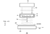
- FIG. 17 is a view showing a digital holographic imaging device 2h according to the fourth embodiment.
- This digital holographic imaging device 2 h includes an additional optical system 60 in addition to the digital holographic imaging device 2 of FIG.
- the beam splitter 62 of the optical system 60 splits the illumination light 12 into the reference light 16 and the object light 17.
- the reference light 16 is reflected by the mirrors 64 and 66 and the beam splitter 68 and is incident on the imaging device 20.
- the object light 17 is irradiated to the test object 4, and the object light 18 acting on the test object 4 passes through the beam splitter 68 and is incident on the imaging device 20.
- An interference pattern of the reference light 16 and the object light 18 is formed on the photoelectric conversion surface 22.
- the present invention is also applicable to a digital holographic imaging device in which the paths of the reference light and the object light are separated in this way.
- the limiting unit 50 may be configured by any of the optical low pass filter 52 and the incident angle limiting units 54 and 56 described above.
- the digital holographic imaging device 2 for measuring the transmitted light of the test object 4 has been described, but it may be of a type for measuring the reflected light.
- test object 4 is a phase object having a phase distribution
- the test object 4 may be an amplitude object having an intensity distribution, or has a phase distribution and an intensity distribution. May be
- the limiting unit 50 may finely vibrate the imaging device 20 or the test object 4 at high speed during the exposure time.
- test object 4 examples include semiconductor devices and metals.
- the present invention is applicable to digital holographic imaging devices.
Landscapes
- Physics & Mathematics (AREA)
- General Physics & Mathematics (AREA)
- Chemical & Material Sciences (AREA)
- Analytical Chemistry (AREA)
- Optics & Photonics (AREA)
- Engineering & Computer Science (AREA)
- Computing Systems (AREA)
- Theoretical Computer Science (AREA)
- Holo Graphy (AREA)
- Microscoopes, Condenser (AREA)
Abstract
Dans la présente invention, une unité d'éclairage (10) éclaire un échantillon (4) à l'aide d'une lumière d'éclairage (12). Un élément d'imagerie (20) comprend une pluralité de pixels agencés de manière bidimensionnelle sur une surface (22) de conversion photoélectrique, et capture une image de la distribution d'intensité d'un motif d'interférence formé par la lumière d'éclairage (14) ayant été appliquée sur l'échantillon (4). Une unité de commande (50) commande la fréquence spatiale du motif d'interférence formé sur la surface (22) de conversion photoélectrique et/ou l'angle d'incidence de la lumière incidente sur la surface (22) de conversion photoélectrique.
Priority Applications (3)
| Application Number | Priority Date | Filing Date | Title |
|---|---|---|---|
| JP2018518890A JPWO2017203661A1 (ja) | 2016-05-26 | 2016-05-26 | デジタルホログラフィック撮像装置 |
| PCT/JP2016/065614 WO2017203661A1 (fr) | 2016-05-26 | 2016-05-26 | Dispositif d'imagerie holographique numérique |
| US16/195,459 US11086272B2 (en) | 2016-05-26 | 2018-11-19 | Digital holographic imaging apparatus |
Applications Claiming Priority (1)
| Application Number | Priority Date | Filing Date | Title |
|---|---|---|---|
| PCT/JP2016/065614 WO2017203661A1 (fr) | 2016-05-26 | 2016-05-26 | Dispositif d'imagerie holographique numérique |
Related Child Applications (1)
| Application Number | Title | Priority Date | Filing Date |
|---|---|---|---|
| US16/195,459 Continuation US11086272B2 (en) | 2016-05-26 | 2018-11-19 | Digital holographic imaging apparatus |
Publications (1)
| Publication Number | Publication Date |
|---|---|
| WO2017203661A1 true WO2017203661A1 (fr) | 2017-11-30 |
Family
ID=60412341
Family Applications (1)
| Application Number | Title | Priority Date | Filing Date |
|---|---|---|---|
| PCT/JP2016/065614 Ceased WO2017203661A1 (fr) | 2016-05-26 | 2016-05-26 | Dispositif d'imagerie holographique numérique |
Country Status (3)
| Country | Link |
|---|---|
| US (1) | US11086272B2 (fr) |
| JP (1) | JPWO2017203661A1 (fr) |
| WO (1) | WO2017203661A1 (fr) |
Families Citing this family (1)
| Publication number | Priority date | Publication date | Assignee | Title |
|---|---|---|---|---|
| US12436497B2 (en) * | 2024-03-15 | 2025-10-07 | Metrolaser, Inc. | System and a method for imaging using lens-less holographic microscopy |
Citations (3)
| Publication number | Priority date | Publication date | Assignee | Title |
|---|---|---|---|---|
| JP2011209395A (ja) * | 2010-03-29 | 2011-10-20 | Seiko Epson Corp | 分光センサー及び角度制限フィルター |
| JP2013508775A (ja) * | 2009-10-20 | 2013-03-07 | ザ リージェンツ オブ ザ ユニバーシティ オブ カリフォルニア | オンチップでの非干渉性のレンズフリーのホログラフィおよび顕微鏡法 |
| JP2014137378A (ja) * | 2013-01-15 | 2014-07-28 | Asahi Glass Co Ltd | 撮像装置用液晶素子および光学ローパスフィルタ |
Family Cites Families (5)
| Publication number | Priority date | Publication date | Assignee | Title |
|---|---|---|---|---|
| US20010007475A1 (en) * | 2000-01-06 | 2001-07-12 | Asahi Kogaku Kogyo Kabushiki Kaisha | Image pickup device and its mounting structure for an optical low-pass filter |
| TWI297470B (en) * | 2005-05-10 | 2008-06-01 | Asmedia Technology Inc | Method for image adjustment |
| US9864184B2 (en) * | 2012-10-30 | 2018-01-09 | California Institute Of Technology | Embedded pupil function recovery for fourier ptychographic imaging devices |
| JP6349202B2 (ja) * | 2014-08-29 | 2018-06-27 | シスメックス株式会社 | 蛍光検出装置、被検物質検出装置、及び蛍光検出方法 |
| WO2016124399A1 (fr) * | 2015-02-06 | 2016-08-11 | Asml Netherlands B.V. | Procédé et appareil pour améliorer une précision de mesure |
-
2016
- 2016-05-26 WO PCT/JP2016/065614 patent/WO2017203661A1/fr not_active Ceased
- 2016-05-26 JP JP2018518890A patent/JPWO2017203661A1/ja active Pending
-
2018
- 2018-11-19 US US16/195,459 patent/US11086272B2/en active Active
Patent Citations (3)
| Publication number | Priority date | Publication date | Assignee | Title |
|---|---|---|---|---|
| JP2013508775A (ja) * | 2009-10-20 | 2013-03-07 | ザ リージェンツ オブ ザ ユニバーシティ オブ カリフォルニア | オンチップでの非干渉性のレンズフリーのホログラフィおよび顕微鏡法 |
| JP2011209395A (ja) * | 2010-03-29 | 2011-10-20 | Seiko Epson Corp | 分光センサー及び角度制限フィルター |
| JP2014137378A (ja) * | 2013-01-15 | 2014-07-28 | Asahi Glass Co Ltd | 撮像装置用液晶素子および光学ローパスフィルタ |
Non-Patent Citations (1)
| Title |
|---|
| TATSUYA NAKATSU JI ET AL: "Acquisition of 3-D 1-9 Image in Large Visual Field by Using Phase- Shift Lensless-Fourier Digital Holography", 3D IMAGE CONFERENCE 2006 KOEN RONBUNSHU, July 2006 (2006-07-01), pages 113 - 116 * |
Also Published As
| Publication number | Publication date |
|---|---|
| JPWO2017203661A1 (ja) | 2019-04-04 |
| US20190086864A1 (en) | 2019-03-21 |
| US11086272B2 (en) | 2021-08-10 |
Similar Documents
| Publication | Publication Date | Title |
|---|---|---|
| US10613478B2 (en) | Imaging method of structured illumination digital holography | |
| JP6494205B2 (ja) | 波面計測方法、形状計測方法、光学素子の製造方法、光学機器の製造方法、プログラム、波面計測装置 | |
| CN110108201B (zh) | 透反射双模式的高精度离轴数字全息显微装置及成像方法 | |
| US20140114188A1 (en) | Acousto-optic vibrometer | |
| JPWO2018221025A1 (ja) | 撮像装置、画像処理装置、撮像システム、画像処理方法、及び記録媒体 | |
| US11275034B2 (en) | Inspection apparatus and method based on coherent diffraction imaging (CDI) | |
| JP2024544161A (ja) | 全光場イメージングカメラ及びそのイメージング方法、並びに全光場イメージング装置 | |
| JPWO2013065796A1 (ja) | 観察装置 | |
| JP5354675B2 (ja) | 変位分布計測方法、装置及びプログラム | |
| JP7348858B2 (ja) | ホログラム撮影装置及び像再構成システム | |
| US20250334525A1 (en) | Optical measurement system and optical measurement method | |
| KR20170079441A (ko) | 진동 환경에서 큰 단차를 갖는 샘플의 높낮이 측정을 위한 디지털 홀로그램 기록재생장치 및 기록재생방법 | |
| EP3994529A1 (fr) | Procédure de déphasage sans étalonnage pour holographie à auto-interférence | |
| WO2017203661A1 (fr) | Dispositif d'imagerie holographique numérique | |
| JP2018021891A (ja) | 光学系の位相取得方法および光学系の評価方法 | |
| JP2007071584A (ja) | デジタルホログラフィを利用した変位分布計測方法及び装置 | |
| JP2013257228A (ja) | 波面測定装置 | |
| JP2009505105A (ja) | 改良型ホログラフィ撮像のためのシステムおよび方法 | |
| US20160320485A1 (en) | Image processing method | |
| JP7737293B2 (ja) | 撮像装置及び撮像方法 | |
| KR20170019954A (ko) | 공초점 표면 측정 장치 및 방법 | |
| CN114208145A (zh) | 摄像装置和方法 | |
| CN207502929U (zh) | 一种层叠衍射成像装置 | |
| CN102506755B (zh) | 基于方向频谱分离的数字全息层析图像记录装置 | |
| JP4025878B2 (ja) | 物体の再生像を得る装置、位相シフトデジタルホログラフィ変位分布計測装置及びパラメータを同定する方法 |
Legal Events
| Date | Code | Title | Description |
|---|---|---|---|
| WWE | Wipo information: entry into national phase |
Ref document number: 2018518890 Country of ref document: JP |
|
| NENP | Non-entry into the national phase |
Ref country code: DE |
|
| 121 | Ep: the epo has been informed by wipo that ep was designated in this application |
Ref document number: 16903142 Country of ref document: EP Kind code of ref document: A1 |
|
| 122 | Ep: pct application non-entry in european phase |
Ref document number: 16903142 Country of ref document: EP Kind code of ref document: A1 |