WO2017203670A1 - Dispositif de mise en forme de lumière - Google Patents
Dispositif de mise en forme de lumière Download PDFInfo
- Publication number
- WO2017203670A1 WO2017203670A1 PCT/JP2016/065642 JP2016065642W WO2017203670A1 WO 2017203670 A1 WO2017203670 A1 WO 2017203670A1 JP 2016065642 W JP2016065642 W JP 2016065642W WO 2017203670 A1 WO2017203670 A1 WO 2017203670A1
- Authority
- WO
- WIPO (PCT)
- Prior art keywords
- light
- laser
- mirror
- housing
- laser diode
- Prior art date
- Legal status (The legal status is an assumption and is not a legal conclusion. Google has not performed a legal analysis and makes no representation as to the accuracy of the status listed.)
- Ceased
Links
Images





Classifications
-
- B—PERFORMING OPERATIONS; TRANSPORTING
- B29—WORKING OF PLASTICS; WORKING OF SUBSTANCES IN A PLASTIC STATE IN GENERAL
- B29C—SHAPING OR JOINING OF PLASTICS; SHAPING OF MATERIAL IN A PLASTIC STATE, NOT OTHERWISE PROVIDED FOR; AFTER-TREATMENT OF THE SHAPED PRODUCTS, e.g. REPAIRING
- B29C64/00—Additive manufacturing, i.e. manufacturing of three-dimensional [3D] objects by additive deposition, additive agglomeration or additive layering, e.g. by 3D printing, stereolithography or selective laser sintering
- B29C64/10—Processes of additive manufacturing
- B29C64/106—Processes of additive manufacturing using only liquids or viscous materials, e.g. depositing a continuous bead of viscous material
- B29C64/124—Processes of additive manufacturing using only liquids or viscous materials, e.g. depositing a continuous bead of viscous material using layers of liquid which are selectively solidified
- B29C64/129—Processes of additive manufacturing using only liquids or viscous materials, e.g. depositing a continuous bead of viscous material using layers of liquid which are selectively solidified characterised by the energy source therefor, e.g. by global irradiation combined with a mask
-
- B—PERFORMING OPERATIONS; TRANSPORTING
- B29—WORKING OF PLASTICS; WORKING OF SUBSTANCES IN A PLASTIC STATE IN GENERAL
- B29C—SHAPING OR JOINING OF PLASTICS; SHAPING OF MATERIAL IN A PLASTIC STATE, NOT OTHERWISE PROVIDED FOR; AFTER-TREATMENT OF THE SHAPED PRODUCTS, e.g. REPAIRING
- B29C64/00—Additive manufacturing, i.e. manufacturing of three-dimensional [3D] objects by additive deposition, additive agglomeration or additive layering, e.g. by 3D printing, stereolithography or selective laser sintering
- B29C64/10—Processes of additive manufacturing
- B29C64/106—Processes of additive manufacturing using only liquids or viscous materials, e.g. depositing a continuous bead of viscous material
-
- B—PERFORMING OPERATIONS; TRANSPORTING
- B29—WORKING OF PLASTICS; WORKING OF SUBSTANCES IN A PLASTIC STATE IN GENERAL
- B29C—SHAPING OR JOINING OF PLASTICS; SHAPING OF MATERIAL IN A PLASTIC STATE, NOT OTHERWISE PROVIDED FOR; AFTER-TREATMENT OF THE SHAPED PRODUCTS, e.g. REPAIRING
- B29C64/00—Additive manufacturing, i.e. manufacturing of three-dimensional [3D] objects by additive deposition, additive agglomeration or additive layering, e.g. by 3D printing, stereolithography or selective laser sintering
- B29C64/20—Apparatus for additive manufacturing; Details thereof or accessories therefor
- B29C64/25—Housings, e.g. machine housings
-
- B—PERFORMING OPERATIONS; TRANSPORTING
- B29—WORKING OF PLASTICS; WORKING OF SUBSTANCES IN A PLASTIC STATE IN GENERAL
- B29C—SHAPING OR JOINING OF PLASTICS; SHAPING OF MATERIAL IN A PLASTIC STATE, NOT OTHERWISE PROVIDED FOR; AFTER-TREATMENT OF THE SHAPED PRODUCTS, e.g. REPAIRING
- B29C64/00—Additive manufacturing, i.e. manufacturing of three-dimensional [3D] objects by additive deposition, additive agglomeration or additive layering, e.g. by 3D printing, stereolithography or selective laser sintering
- B29C64/20—Apparatus for additive manufacturing; Details thereof or accessories therefor
- B29C64/264—Arrangements for irradiation
-
- B—PERFORMING OPERATIONS; TRANSPORTING
- B29—WORKING OF PLASTICS; WORKING OF SUBSTANCES IN A PLASTIC STATE IN GENERAL
- B29C—SHAPING OR JOINING OF PLASTICS; SHAPING OF MATERIAL IN A PLASTIC STATE, NOT OTHERWISE PROVIDED FOR; AFTER-TREATMENT OF THE SHAPED PRODUCTS, e.g. REPAIRING
- B29C64/00—Additive manufacturing, i.e. manufacturing of three-dimensional [3D] objects by additive deposition, additive agglomeration or additive layering, e.g. by 3D printing, stereolithography or selective laser sintering
- B29C64/20—Apparatus for additive manufacturing; Details thereof or accessories therefor
- B29C64/264—Arrangements for irradiation
- B29C64/268—Arrangements for irradiation using laser beams; using electron beams [EB]
-
- B—PERFORMING OPERATIONS; TRANSPORTING
- B29—WORKING OF PLASTICS; WORKING OF SUBSTANCES IN A PLASTIC STATE IN GENERAL
- B29C—SHAPING OR JOINING OF PLASTICS; SHAPING OF MATERIAL IN A PLASTIC STATE, NOT OTHERWISE PROVIDED FOR; AFTER-TREATMENT OF THE SHAPED PRODUCTS, e.g. REPAIRING
- B29C67/00—Shaping techniques not covered by groups B29C39/00 - B29C65/00, B29C70/00 or B29C73/00
-
- B—PERFORMING OPERATIONS; TRANSPORTING
- B33—ADDITIVE MANUFACTURING TECHNOLOGY
- B33Y—ADDITIVE MANUFACTURING, i.e. MANUFACTURING OF THREE-DIMENSIONAL [3D] OBJECTS BY ADDITIVE DEPOSITION, ADDITIVE AGGLOMERATION OR ADDITIVE LAYERING, e.g. BY 3D PRINTING, STEREOLITHOGRAPHY OR SELECTIVE LASER SINTERING
- B33Y30/00—Apparatus for additive manufacturing; Details thereof or accessories therefor
-
- B—PERFORMING OPERATIONS; TRANSPORTING
- B29—WORKING OF PLASTICS; WORKING OF SUBSTANCES IN A PLASTIC STATE IN GENERAL
- B29K—INDEXING SCHEME ASSOCIATED WITH SUBCLASSES B29B, B29C OR B29D, RELATING TO MOULDING MATERIALS OR TO MATERIALS FOR MOULDS, REINFORCEMENTS, FILLERS OR PREFORMED PARTS, e.g. INSERTS
- B29K2105/00—Condition, form or state of moulded material or of the material to be shaped
- B29K2105/0058—Liquid or visquous
Definitions
- the present invention relates to an optical modeling apparatus.
- Patent Document 1 discloses a three-dimensional stereolithography technique based on a continuous liquid bonding method.
- An object of the present invention is to provide a technique for solving the above-described problems.
- an apparatus provides: A material tank having a bottom surface formed of a light-transmitting material, and a material tank for storing a light-curable liquid material; A light source unit with a built-in drive mirror that scans the bottom surface of the laser beam; A lifting mechanism for lifting a modeled object modeled with the laser light from the resin tank; With The light source unit is an optical engine, A housing, A laser diode that is disposed on one side of the housing and emits laser light; The drive mirror that reflects the reflected light from the laser diode while changing the angle in the vertical and horizontal directions; Is an optical modeling apparatus.
- another apparatus provides: A material tank having a bottom surface formed of a light-transmitting material, and a material tank for storing a light-curable liquid material; A stand for installing a smart device incorporating an optical engine that scans the bottom surface with a laser beam; A lifting mechanism for lifting a modeled object modeled with the laser light from the resin tank; Is an optical modeling apparatus.
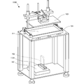
- the information processing apparatus 100 is a pull-up type continuous liquid bond modeling apparatus.
- the information processing apparatus 100 includes a material tank 101, a light source unit 102, and a lifting mechanism 103.
- the material tank 101 is a material tank in which at least the bottom surface 111 is formed of a light transmissive material, and accommodates a light curable liquid material.
- the light source unit 102 is a smart device incorporating a micro laser projector, and scans the bottom surface 111 of the material tank 101 with laser light 121 from below.
- the lifting mechanism 103 lifts the modeled object modeled with the laser beam 121 from the material tank 101 according to the stacking pitch.
- the laser beam 121 is applied and cured, the modeling table is further raised, and the cross-sectional shape of the second layer is repeatedly cured below, and the layers are sequentially stacked and modeled.
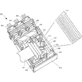
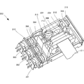
- FIGS. 2A, 2B, and 2 are perspective views of the internal configuration of the optical engine 200 as seen from different angles.
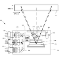
- FIG. 2C is a diagram showing an optical path in the optical engine 200.
- the optical engine 200 includes, for example, three colors of laser diodes (semiconductor lasers) 201 to 203 of red, infrared light, and ultraviolet light, and a prism mirror 204 for collecting the light beams from the laser diodes 201 to 203 into one light beam. , including.
- the laser diode 201 emits ultraviolet light
- the laser diode 202 emits ultraviolet light
- the laser diode 203 emits infrared light.
- the short wavelength ones are arranged in order so as to be the farthest from the MEMS.
- the laser diodes 201 to 203 are arranged side by side toward the inside of the casing 210 on one side of the casing 210.
- the prism mirror 204 once reflects two laser beams from the laser diodes 201 and 202 once toward the laser diode 203 side. Further, the two reflected lights are reflected again toward the inside of the casing 210 so as to overlap the optical axis of the laser diode 203.
- the optical engine 200 includes a collimator lens 205 between the laser diodes 201 to 203 and the prism mirror 204, and adjusts the focal length of the laser light to infinity.
- An inclined mirror 206 that is inclined toward the bottom surface is provided at the end of the housing 210 opposite to the mounting surface of the laser diodes 201 to 203.
- the tilt mirror 206 reflects the laser beam incident from the prism mirror 204 toward the bottom surface of the housing 210.
- a bottom mirror 207 is mounted upward on the bottom surface of the casing 210 between the prism mirror 204 and the tilt mirror 206.
- a two-dimensional MEMS mirror 209 and a cover glass 212 are provided so as to sandwich the bottom mirror 207.
- the bottom mirror 207 reflects the laser beam incident from the inclined mirror 206 upward toward the two-dimensional MEMS mirror 209.
- a prism 208 that determines the image projection elevation angle and size is provided at a position adjacent to the two-dimensional MEMS mirror 209 and on the cover glass 212 side.
- another bottom mirror 213 is provided between the bottom mirror 207 and the cover glass 212.
- a photo sensor 215 is provided between the prism mirror 204 and the prism 208. In order to calibrate the position of the MEMS mirror 209, the photosensor 215 transmits the timing at which the light beam is incident from the MEMS mirror 209 via the bottom mirror 213 to an external MEMS control unit.
- the inclined mirror 206 is a semi-transmissive mirror, and a laser power sensor 216 is provided on the rear side thereof, that is, in the gap between the wall portion of the casing 210 and the inclined mirror 206, and detects the laser power. To the external laser scan display controller.
- the projection image is formed on the bottom surface 111 by the scanning light beam reflected by the MEMS mirror 209 and passing through the prism 208 and the cover glass 212.
- the three light beams from the laser diodes 201 to 203 are incident on the prism mirror 204 via the collimator lens 205 and are combined into one light beam.
- the light beam emitted from the prism mirror 204 is reflected by the tilt mirror 206 and travels toward the bottom mirror 207.
- the bottom mirror 207 reflects light incident from the inclined mirror 206 upward, and enters the central portion of the two-dimensional MEMS mirror 209 via the prism 208.
- the two-dimensional MEMS mirror 209 is a drive mirror that is driven based on a control signal input from the outside, and vibrates so as to reflect light rays by changing the angle in the horizontal direction (X direction) and the vertical direction (Y direction). .
- FIG. 3 is a diagram illustrating a configuration of a laser projector 300 including the optical engine 200.
- FIG. 4 is a functional configuration diagram of the laser projector 300.
- the optical engine 200 includes a laser diode (LD in the figure) drive unit 311 and a power management circuit 312 in addition to the components described with reference to FIGS. 2A and 2B.
- LD laser diode
- the laser projector 300 includes a MEMS control unit 301 and a laser scan display control unit 302.
- the laser scan display control unit 302 When the digital video signal is input from the outside, the laser scan display control unit 302 extracts the number of pixels and the size and transmits the extracted pixel number and size to the MEMS control unit 301. In addition, the laser scan display control unit 302 decomposes the digital video signal into pixel data of each color and sends the pixel data to the laser diode drive unit 311.
- the power management circuits (PMCs) 312 controls the laser diode driving unit 311 so that it does not malfunction in an initial transient period, for example, a rising period (falling period) or a falling period (falling period). In particular, during the transition period, the output voltage may be lower than the required voltage.
- the laser diode driver 311 may malfunction due to a low voltage and / or voltage fluctuation. In order to avoid such a problem, the functional circuit block can be placed in a reset state during the transition period.
- the laser power sensor 216 controls the illuminance of each color of the laser diodes 201 to 203 by detecting the power of each color of the laser transmitted through the tilt mirror 206 and feeding back the power data to the laser scan display control unit 302. .
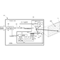
- FIG. 4 is a functional configuration diagram of the light source unit 102 including the optical engine 200.
- the digital video signal input to the laser scan display controller 302 is modulated here and sent to the laser diode driver 311.
- the laser diode driver 311 controls the brightness and irradiation timing of the laser that is projected by driving each color LED.
- the laser scan display control unit 302 simultaneously drives the MEMS control unit 301 to vibrate the MEMS mirror 209 biaxially under optimal conditions.
- the power management circuit 312 controls the laser diode driver 311 to cause the laser diodes 201 to 203 to emit light at an appropriate voltage and timing.
- Laser light reflected by the two-dimensional MEMS mirror 209 through the collimator lens 205 and the optical systems 204 and 206 is projected onto the bottom surface 110 as modeling laser light.
- the MEMS scanning method as described above is overwhelmingly more efficient in using light than DLP. Therefore, the same modeling as DLP becomes possible with an overwhelming low power laser. In other words, it is possible to reduce the price, save power, and reduce the size while achieving high accuracy.
- the laser beam can be narrowed down ( ⁇ 0.8mm ⁇ 0.02mm) to improve the modeling accuracy.
- the modeling area can be changed by changing the irradiation distance of the optical engine.
- the modeling area can be changed by software without changing the irradiation distance of the optical engine. Therefore, it is possible to change the modeling area while keeping the pulling speed constant.
- the total power of the laser diode can be increased by changing the number of laser diodes assembled in the optical engine. For example, an output of 60 mW can be realized using three laser diodes of 20 mW.
- a high output optical engine can be realized by assembling a plurality of laser diodes as light sources having the same wavelength.
- ⁇ Sharp / soft modeling can be selected at any location by combining multiple laser diodes that emit lasers with the same wavelength and different beam diameters.
- ⁇ Two types of laser wavelengths infrared light and ultraviolet light, are installed, and can be automatically generated at a predetermined position with ultraviolet light while detecting the position with an infrared laser.
- the infrared laser serves as guide light.
- the power of the edge part of a cross-sectional shape can be strengthened, or it can also be weakened to prevent punch-through hardening in inclined molding or the like. Power control according to the shape is possible.
- ⁇ Steps on the modeling surface can be changed by changing the spot diameter.
- FIG. 5 is a diagram showing a device in the configuration of the optical system for realizing miniaturization.
- the configuration 502 of the present embodiment is devised in the following three points in order to realize ultra-small size, improved reliability, and improved production efficiency.
- small laser diodes 201 to 203 were arranged in close proximity.
- the MEMS mirror 209 itself is also smaller than the premise configuration 501.
- the laser diode 513 is first adjusted with respect to the target.
- the adjustment contents at that time were the position of the mirror 516 (biaxial direction), the position of the MEMS mirror 519 (biaxial direction), and a collimator lens (not shown) (5-axis direction).
- Adjust the beam size by confirming that a laser beam spot of a predetermined position and size is formed within the adjustment range and that the reflected light from the hinge of the MEMS mirror 519 does not appear in the projected image.
- the collimator lens, the mirror 516, and the MEMS mirror 519 are bonded and fixed.
- collimator lens (5-axis position) adjustment was performed targeting a position away from the MEMS mirror 519 by a predetermined distance after completion of adjustment adhesion of the center laser diode.
- a housing 210 as a die-cast housing shown in FIG. 6 is used, and optical components other than the collimator lens and the laser diode are abutted against and bonded to the positioning portion of the housing 210 in advance.
- the prism mirror 204 is arranged close to the corner of the positioning unit 601.
- the MEMS mirror 209 is disposed in contact with the positioning surfaces 602 and 603.
- the inclined mirror 206 is disposed in contact with the positioning surfaces 604 and 605.
- the bottom mirror 207 is attached to the positioning surface 606.
- the prism 208 is attached in contact with the positioning surfaces 607 and 608.
- the number of adjustment points was reduced from 3 parts of the premise technology configuration 501 to 2 parts (collimator lens 205 and laser diodes 201 to 203). Since the housing 210 is a non-cutting and non-machined housing, the accuracy and production efficiency are remarkably good, and it is suitable for mass production. Note that a molded product using a mold such as a resin may be used as the casing 210.
- two inclined surfaces for positioning each of the collimator holders are prepared at positions where collimator lenses (actually, collimator lens holders) are arranged. Yes.
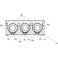
- FIG. 7 is a view for explaining a method of fixing the collimator holder, and is a cross-sectional view taken along the line AA in FIG.
- a laser diode is press-fitted into the housing, a collimator holder with a collimator lens bonded and fixed is placed on the housing at an optically appropriate position by spatial adjustment, and a UV adhesive is placed between the housing and the collimator holder. Pour UV radiation cure.
- the position of the collimator holder fluctuates because the adhesive shrinks in volume during the UV irradiation fixation.
- the irradiation amount and direction of the UV light are devised while monitoring the beam fluctuation direction, and fixed at a predetermined position.
- the blue and red beam positions need to coincide with green, and the adjustment work is extremely difficult.
- the beam position fluctuates due to the stress relaxation of the adhesive in the QA test such as the cooling test.
- the collimator lens 205 (collimator holder) is brought into contact with the inclined surface 609 provided in the housing 210 and firmly positioned.
- the adhesive 701 is injected from the injection port 702 provided on the lower surface of the housing 210, and after waiting for a certain time, the collimator lens 205 can be firmly fixed at the target position. Since the components are fixed in a state where they are in direct contact rather than so-called space bonding, the position of each component does not change due to shrinkage of the adhesive, and stability and reliability are greatly improved.
- the laser diodes 201 to 203 (X-axis and Y-axis two-axis positions) and the collimator lens 205 (Z-axis one axis) are used.
- Production efficiency can be improved. In other words, mass production is extremely easy because the production system can be used for precision adjustment and skill-free and automated work that does not select workers.
- the spot position can be adjusted to a predetermined size and position to greatly improve the beam position variation.
- the laser projector 300 has been described above. Since the laser projector 300 is very small and thin as described above, it can be mounted inside a thin smartphone 1000 as shown in FIG.
- FIG. 1 is a diagram for explaining the configuration of the additive manufacturing apparatus according to the present embodiment.
- the additive manufacturing apparatus according to the present embodiment is different from the first embodiment in that it does not have a light source unit. Since other configurations and operations are the same as those in the first embodiment, the same configurations and operations are denoted by the same reference numerals, and detailed description thereof is omitted.
- an additive manufacturing apparatus 1100 having no light source and having only a smart device stand 1101 can be manufactured and sold. It becomes possible. If the user can configure the 3D printer simply by pointing his / her smart device to the stand 1101, the manufacturing efficiency of the additive manufacturing apparatus 1100 can be increased, and the 3D printer can be provided at a low cost.
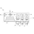
- FIG. 12 is a diagram for explaining the configuration of the optical engine according to the present embodiment.
- the optical engine according to the present embodiment does not have the photo sensor 215 and the bottom mirror 213 and is different in the arrangement of the other components as compared with the first embodiment. Since other configurations and operations are the same as those in the first embodiment, the same configurations and operations are denoted by the same reference numerals, and detailed description thereof is omitted. If the layout is as shown in FIG. 12, it is possible to further reduce the size while maintaining the image quality.
Landscapes
- Engineering & Computer Science (AREA)
- Chemical & Material Sciences (AREA)
- Materials Engineering (AREA)
- Mechanical Engineering (AREA)
- Manufacturing & Machinery (AREA)
- Physics & Mathematics (AREA)
- Optics & Photonics (AREA)
- Health & Medical Sciences (AREA)
- Toxicology (AREA)
- Plasma & Fusion (AREA)
- Mechanical Optical Scanning Systems (AREA)
- Semiconductor Lasers (AREA)
Abstract
L'invention concerne un dispositif de mise en forme de lumière qui permet d'effectuer simplement, facilement et suffisamment précisément une mise en forme tridimensionnelle et qui est pourvu : d'un réservoir de matériau ayant une surface inférieure faite d'un matériau de transmission de lumière et recevant un matériau liquide photodurcissable ; d'une unité de source de lumière ayant un miroir d'activation intégré qui balaie la surface inférieure au moyen de la lumière laser ; d'un mécanisme de levage qui lève un objet façonné, formé par la lumière laser, se trouvant dans un réservoir de résine. L'unité de source de lumière possède, en tant que moteur optique, un boîtier, une diode laser qui est agencée sur un côté dans le boîtier et qui émet la lumière laser, et un miroir d'activation qui réfléchit la lumière de réflexion provenant de la diode laser tout en changeant son angle dans une direction verticale et une direction horizontale.
Priority Applications (4)
| Application Number | Priority Date | Filing Date | Title |
|---|---|---|---|
| CN201680024592.8A CN107660178B (zh) | 2016-05-26 | 2016-05-26 | 光学成型设备 |
| PCT/JP2016/065642 WO2017203670A1 (fr) | 2016-05-26 | 2016-05-26 | Dispositif de mise en forme de lumière |
| US15/569,058 US20180222108A1 (en) | 2016-05-26 | 2016-05-26 | Optical shaping apparatus |
| US17/373,512 US20210339460A1 (en) | 2016-05-26 | 2021-07-12 | Optical shaping apparatus |
Applications Claiming Priority (1)
| Application Number | Priority Date | Filing Date | Title |
|---|---|---|---|
| PCT/JP2016/065642 WO2017203670A1 (fr) | 2016-05-26 | 2016-05-26 | Dispositif de mise en forme de lumière |
Related Child Applications (2)
| Application Number | Title | Priority Date | Filing Date |
|---|---|---|---|
| US15/569,058 A-371-Of-International US20180222108A1 (en) | 2016-05-26 | 2016-05-26 | Optical shaping apparatus |
| US17/373,512 Continuation US20210339460A1 (en) | 2016-05-26 | 2021-07-12 | Optical shaping apparatus |
Publications (1)
| Publication Number | Publication Date |
|---|---|
| WO2017203670A1 true WO2017203670A1 (fr) | 2017-11-30 |
Family
ID=60411242
Family Applications (1)
| Application Number | Title | Priority Date | Filing Date |
|---|---|---|---|
| PCT/JP2016/065642 Ceased WO2017203670A1 (fr) | 2016-05-26 | 2016-05-26 | Dispositif de mise en forme de lumière |
Country Status (3)
| Country | Link |
|---|---|
| US (2) | US20180222108A1 (fr) |
| CN (1) | CN107660178B (fr) |
| WO (1) | WO2017203670A1 (fr) |
Families Citing this family (5)
| Publication number | Priority date | Publication date | Assignee | Title |
|---|---|---|---|---|
| JP6668004B2 (ja) * | 2015-06-09 | 2020-03-18 | カンタツ株式会社 | 回路パターン製造装置、回路パターン製造方法および回路パターン製造プログラム |
| JP6892727B2 (ja) | 2016-09-26 | 2021-06-23 | カンタツ株式会社 | パターン製造装置、パターン製造方法およびパターン製造プログラム |
| JP6839476B2 (ja) | 2016-09-26 | 2021-03-10 | カンタツ株式会社 | パターン形成用シート |
| JP2018182126A (ja) | 2017-04-17 | 2018-11-15 | カンタツ株式会社 | パターン形成用シート、パターン製造装置およびパターン製造方法 |
| JP2019193995A (ja) * | 2018-05-02 | 2019-11-07 | カンタツ株式会社 | 積層造形装置および積層造形装置の制御方法 |
Citations (2)
| Publication number | Priority date | Publication date | Assignee | Title |
|---|---|---|---|---|
| JP2000238137A (ja) * | 1999-02-17 | 2000-09-05 | Mitsubishi Heavy Ind Ltd | 光造形装置及び光造形方法 |
| JP2003039564A (ja) * | 2001-04-20 | 2003-02-13 | Envision Technologies Gmbh | 3次元物体を生成するための装置 |
Family Cites Families (3)
| Publication number | Priority date | Publication date | Assignee | Title |
|---|---|---|---|---|
| JP5880443B2 (ja) * | 2010-12-13 | 2016-03-09 | 株式会社ニコン | 露光方法、露光装置、及びデバイス製造方法 |
| US9636873B2 (en) * | 2012-05-03 | 2017-05-02 | B9Creations, LLC | Solid image apparatus with improved part separation from the image plate |
| WO2016063665A1 (fr) * | 2014-10-20 | 2016-04-28 | ソニー株式会社 | Appareil de moulage optique et procédé pour la fabrication d'un objet moulé |
-
2016
- 2016-05-26 WO PCT/JP2016/065642 patent/WO2017203670A1/fr not_active Ceased
- 2016-05-26 US US15/569,058 patent/US20180222108A1/en not_active Abandoned
- 2016-05-26 CN CN201680024592.8A patent/CN107660178B/zh not_active Expired - Fee Related
-
2021
- 2021-07-12 US US17/373,512 patent/US20210339460A1/en not_active Abandoned
Patent Citations (2)
| Publication number | Priority date | Publication date | Assignee | Title |
|---|---|---|---|---|
| JP2000238137A (ja) * | 1999-02-17 | 2000-09-05 | Mitsubishi Heavy Ind Ltd | 光造形装置及び光造形方法 |
| JP2003039564A (ja) * | 2001-04-20 | 2003-02-13 | Envision Technologies Gmbh | 3次元物体を生成するための装置 |
Also Published As
| Publication number | Publication date |
|---|---|
| US20210339460A1 (en) | 2021-11-04 |
| US20180222108A1 (en) | 2018-08-09 |
| CN107660178A (zh) | 2018-02-02 |
| CN107660178B (zh) | 2019-10-25 |
Similar Documents
| Publication | Publication Date | Title |
|---|---|---|
| JP6357440B2 (ja) | 光造形装置 | |
| US20210339460A1 (en) | Optical shaping apparatus | |
| JP5336600B2 (ja) | 発光装置及びその製造方法 | |
| US20190196205A1 (en) | Grating waveguide combiner for optical engine | |
| CN116157735A (zh) | 投影模组及其组装方法和包括投影模组的近眼显示设备 | |
| CN110351454A (zh) | 红外相机模块及其图像传感器以及电子装置 | |
| US10933578B2 (en) | Pattern forming sheet, pattern manufacturing apparatus, and pattern manufacturing method | |
| EP3502761A1 (fr) | Unité de source de lumière | |
| US20220019147A1 (en) | Circuit pattern forming sheet, circuit pattern manufacturing apparatus, circuit pattern manufacturing method, and circuit pattern manufacturing program | |
| JP6457185B2 (ja) | 光学エンジンおよびその製造方法、ならびにプロジェクタ | |
| CN107031035A (zh) | 立体物件成型系统及其校正方法 | |
| CN208798114U (zh) | 投影模组、成像装置和电子装置 | |
| US9122146B2 (en) | Optical module used in projection device | |
| JP2018138393A (ja) | 光造形装置 | |
| US8052290B2 (en) | Rear-projection-type display apparatus | |
| KR101903251B1 (ko) | 3d프린팅용 광원모듈 및 3d프린터 | |
| CN110320673A (zh) | 光学模块和用于投影的方法 | |
| WO2014045340A1 (fr) | Élément optique, source lumineuse et affichage tête haute | |
| CN113238387A (zh) | 一种复眼镜片模组、照明装置及dlp光机模组 | |
| JP2019079061A (ja) | 光学エンジンおよびその製造方法、ならびにプロジェクタ | |
| US10908383B1 (en) | Local control loop for projection system focus adjustment | |
| WO2022233086A1 (fr) | Procédé de fabrication d'un module de lentille oculaire composite | |
| KR102306124B1 (ko) | 레이저 스캔 프로젝터 모듈 및 그 제조방법 | |
| US20250334676A1 (en) | Optical sensor and manufacturing method | |
| KR100484201B1 (ko) | 광주사장치 |
Legal Events
| Date | Code | Title | Description |
|---|---|---|---|
| WWE | Wipo information: entry into national phase |
Ref document number: 15569058 Country of ref document: US |
|
| NENP | Non-entry into the national phase |
Ref country code: DE |
|
| 121 | Ep: the epo has been informed by wipo that ep was designated in this application |
Ref document number: 16903151 Country of ref document: EP Kind code of ref document: A1 |
|
| 122 | Ep: pct application non-entry in european phase |
Ref document number: 16903151 Country of ref document: EP Kind code of ref document: A1 |
|
| NENP | Non-entry into the national phase |
Ref country code: JP |