WO2017204331A1 - Photodétecteur - Google Patents
Photodétecteur Download PDFInfo
- Publication number
- WO2017204331A1 WO2017204331A1 PCT/JP2017/019698 JP2017019698W WO2017204331A1 WO 2017204331 A1 WO2017204331 A1 WO 2017204331A1 JP 2017019698 W JP2017019698 W JP 2017019698W WO 2017204331 A1 WO2017204331 A1 WO 2017204331A1
- Authority
- WO
- WIPO (PCT)
- Prior art keywords
- light
- light receiving
- optical sensor
- incident
- receiving element
- Prior art date
- Legal status (The legal status is an assumption and is not a legal conclusion. Google has not performed a legal analysis and makes no representation as to the accuracy of the status listed.)
- Ceased
Links
Images





Classifications
-
- H—ELECTRICITY
- H10—SEMICONDUCTOR DEVICES; ELECTRIC SOLID-STATE DEVICES NOT OTHERWISE PROVIDED FOR
- H10F—INORGANIC SEMICONDUCTOR DEVICES SENSITIVE TO INFRARED RADIATION, LIGHT, ELECTROMAGNETIC RADIATION OF SHORTER WAVELENGTH OR CORPUSCULAR RADIATION
- H10F55/00—Radiation-sensitive semiconductor devices covered by groups H10F10/00, H10F19/00 or H10F30/00 being structurally associated with electric light sources and electrically or optically coupled thereto
- H10F55/10—Radiation-sensitive semiconductor devices covered by groups H10F10/00, H10F19/00 or H10F30/00 being structurally associated with electric light sources and electrically or optically coupled thereto wherein the radiation-sensitive semiconductor devices control the electric light source, e.g. image converters, image amplifiers or image storage devices
- H10F55/15—Radiation-sensitive semiconductor devices covered by groups H10F10/00, H10F19/00 or H10F30/00 being structurally associated with electric light sources and electrically or optically coupled thereto wherein the radiation-sensitive semiconductor devices control the electric light source, e.g. image converters, image amplifiers or image storage devices wherein the radiation-sensitive devices and the electric light source are all semiconductor devices
- H10F55/155—Radiation-sensitive semiconductor devices covered by groups H10F10/00, H10F19/00 or H10F30/00 being structurally associated with electric light sources and electrically or optically coupled thereto wherein the radiation-sensitive semiconductor devices control the electric light source, e.g. image converters, image amplifiers or image storage devices wherein the radiation-sensitive devices and the electric light source are all semiconductor devices formed in, or on, a common substrate
-
- G—PHYSICS
- G01—MEASURING; TESTING
- G01S—RADIO DIRECTION-FINDING; RADIO NAVIGATION; DETERMINING DISTANCE OR VELOCITY BY USE OF RADIO WAVES; LOCATING OR PRESENCE-DETECTING BY USE OF THE REFLECTION OR RERADIATION OF RADIO WAVES; ANALOGOUS ARRANGEMENTS USING OTHER WAVES
- G01S17/00—Systems using the reflection or reradiation of electromagnetic waves other than radio waves, e.g. lidar systems
- G01S17/02—Systems using the reflection of electromagnetic waves other than radio waves
- G01S17/04—Systems determining the presence of a target
-
- G—PHYSICS
- G02—OPTICS
- G02B—OPTICAL ELEMENTS, SYSTEMS OR APPARATUS
- G02B5/00—Optical elements other than lenses
- G02B5/20—Filters
- G02B5/28—Interference filters
- G02B5/284—Interference filters of etalon type comprising a resonant cavity other than a thin solid film, e.g. gas, air, solid plates
-
- H—ELECTRICITY
- H10—SEMICONDUCTOR DEVICES; ELECTRIC SOLID-STATE DEVICES NOT OTHERWISE PROVIDED FOR
- H10F—INORGANIC SEMICONDUCTOR DEVICES SENSITIVE TO INFRARED RADIATION, LIGHT, ELECTROMAGNETIC RADIATION OF SHORTER WAVELENGTH OR CORPUSCULAR RADIATION
- H10F30/00—Individual radiation-sensitive semiconductor devices in which radiation controls the flow of current through the devices, e.g. photodetectors
- H10F30/20—Individual radiation-sensitive semiconductor devices in which radiation controls the flow of current through the devices, e.g. photodetectors the devices having potential barriers, e.g. phototransistors
- H10F30/21—Individual radiation-sensitive semiconductor devices in which radiation controls the flow of current through the devices, e.g. photodetectors the devices having potential barriers, e.g. phototransistors the devices being sensitive to infrared, visible or ultraviolet radiation
- H10F30/22—Individual radiation-sensitive semiconductor devices in which radiation controls the flow of current through the devices, e.g. photodetectors the devices having potential barriers, e.g. phototransistors the devices being sensitive to infrared, visible or ultraviolet radiation the devices having only one potential barrier, e.g. photodiodes
- H10F30/221—Individual radiation-sensitive semiconductor devices in which radiation controls the flow of current through the devices, e.g. photodetectors the devices having potential barriers, e.g. phototransistors the devices being sensitive to infrared, visible or ultraviolet radiation the devices having only one potential barrier, e.g. photodiodes the potential barrier being a PN homojunction
-
- H—ELECTRICITY
- H10—SEMICONDUCTOR DEVICES; ELECTRIC SOLID-STATE DEVICES NOT OTHERWISE PROVIDED FOR
- H10F—INORGANIC SEMICONDUCTOR DEVICES SENSITIVE TO INFRARED RADIATION, LIGHT, ELECTROMAGNETIC RADIATION OF SHORTER WAVELENGTH OR CORPUSCULAR RADIATION
- H10F30/00—Individual radiation-sensitive semiconductor devices in which radiation controls the flow of current through the devices, e.g. photodetectors
- H10F30/20—Individual radiation-sensitive semiconductor devices in which radiation controls the flow of current through the devices, e.g. photodetectors the devices having potential barriers, e.g. phototransistors
- H10F30/21—Individual radiation-sensitive semiconductor devices in which radiation controls the flow of current through the devices, e.g. photodetectors the devices having potential barriers, e.g. phototransistors the devices being sensitive to infrared, visible or ultraviolet radiation
- H10F30/22—Individual radiation-sensitive semiconductor devices in which radiation controls the flow of current through the devices, e.g. photodetectors the devices having potential barriers, e.g. phototransistors the devices being sensitive to infrared, visible or ultraviolet radiation the devices having only one potential barrier, e.g. photodiodes
- H10F30/225—Individual radiation-sensitive semiconductor devices in which radiation controls the flow of current through the devices, e.g. photodetectors the devices having potential barriers, e.g. phototransistors the devices being sensitive to infrared, visible or ultraviolet radiation the devices having only one potential barrier, e.g. photodiodes the potential barrier working in avalanche mode, e.g. avalanche photodiodes
-
- H—ELECTRICITY
- H10—SEMICONDUCTOR DEVICES; ELECTRIC SOLID-STATE DEVICES NOT OTHERWISE PROVIDED FOR
- H10F—INORGANIC SEMICONDUCTOR DEVICES SENSITIVE TO INFRARED RADIATION, LIGHT, ELECTROMAGNETIC RADIATION OF SHORTER WAVELENGTH OR CORPUSCULAR RADIATION
- H10F55/00—Radiation-sensitive semiconductor devices covered by groups H10F10/00, H10F19/00 or H10F30/00 being structurally associated with electric light sources and electrically or optically coupled thereto
- H10F55/20—Radiation-sensitive semiconductor devices covered by groups H10F10/00, H10F19/00 or H10F30/00 being structurally associated with electric light sources and electrically or optically coupled thereto wherein the electric light source controls the radiation-sensitive semiconductor devices, e.g. optocouplers
- H10F55/25—Radiation-sensitive semiconductor devices covered by groups H10F10/00, H10F19/00 or H10F30/00 being structurally associated with electric light sources and electrically or optically coupled thereto wherein the electric light source controls the radiation-sensitive semiconductor devices, e.g. optocouplers wherein the radiation-sensitive devices and the electric light source are all semiconductor devices
- H10F55/255—Radiation-sensitive semiconductor devices covered by groups H10F10/00, H10F19/00 or H10F30/00 being structurally associated with electric light sources and electrically or optically coupled thereto wherein the electric light source controls the radiation-sensitive semiconductor devices, e.g. optocouplers wherein the radiation-sensitive devices and the electric light source are all semiconductor devices formed in, or on, a common substrate
-
- H—ELECTRICITY
- H10—SEMICONDUCTOR DEVICES; ELECTRIC SOLID-STATE DEVICES NOT OTHERWISE PROVIDED FOR
- H10F—INORGANIC SEMICONDUCTOR DEVICES SENSITIVE TO INFRARED RADIATION, LIGHT, ELECTROMAGNETIC RADIATION OF SHORTER WAVELENGTH OR CORPUSCULAR RADIATION
- H10F77/00—Constructional details of devices covered by this subclass
- H10F77/30—Coatings
- H10F77/306—Coatings for devices having potential barriers
- H10F77/331—Coatings for devices having potential barriers for filtering or shielding light, e.g. multicolour filters for photodetectors
- H10F77/334—Coatings for devices having potential barriers for filtering or shielding light, e.g. multicolour filters for photodetectors for shielding light, e.g. light blocking layers or cold shields for infrared detectors
-
- H—ELECTRICITY
- H10—SEMICONDUCTOR DEVICES; ELECTRIC SOLID-STATE DEVICES NOT OTHERWISE PROVIDED FOR
- H10F—INORGANIC SEMICONDUCTOR DEVICES SENSITIVE TO INFRARED RADIATION, LIGHT, ELECTROMAGNETIC RADIATION OF SHORTER WAVELENGTH OR CORPUSCULAR RADIATION
- H10F77/00—Constructional details of devices covered by this subclass
- H10F77/30—Coatings
- H10F77/306—Coatings for devices having potential barriers
- H10F77/331—Coatings for devices having potential barriers for filtering or shielding light, e.g. multicolour filters for photodetectors
- H10F77/337—Coatings for devices having potential barriers for filtering or shielding light, e.g. multicolour filters for photodetectors using interference filters, e.g. multilayer dielectric filters
-
- H—ELECTRICITY
- H10—SEMICONDUCTOR DEVICES; ELECTRIC SOLID-STATE DEVICES NOT OTHERWISE PROVIDED FOR
- H10F—INORGANIC SEMICONDUCTOR DEVICES SENSITIVE TO INFRARED RADIATION, LIGHT, ELECTROMAGNETIC RADIATION OF SHORTER WAVELENGTH OR CORPUSCULAR RADIATION
- H10F77/00—Constructional details of devices covered by this subclass
- H10F77/50—Encapsulations or containers
Definitions
- the present invention relates to an optical sensor.
- an automatic robot such as a camera autofocus or a robot cleaner is provided with a distance measuring sensor used for distance or position detection.
- the short distance sensor is an optical sensor for detecting an object to be detected at a short distance, and generally, a photodiode that performs detection judgment by a photocurrent generated by receiving light is used as a light receiving element.
- SPAD is generally used as an optical sensor for detecting an object to be detected at a distance farther than a proximity sensor.
- SPAD is a type of photodiode that is used in a state where an avalanche breakdown occurs when a voltage higher than the withstand voltage is applied, and has an amplification factor as high as 10,000 to 1,000,000 times that of incident optical carriers.
- the sensitivity is high enough to detect single photons.
- Patent Document 1 As such an optical sensor, there is one described in Patent Document 1.
- the optical sensor of Patent Document 1 includes a light emitting element and a light receiving element, and a diffraction grating is provided on a light path that is irradiated from the light emitting element, reflected by a light-transmitting plate, and directed toward the light receiving element. The intensity of light traveling toward the light receiving element without being reflected by the detected object is reduced.
- the diffraction grating is designed for light of a specific wavelength, for example, when a light emitting element emits light of a wavelength in a predetermined band, the specific wavelength designed In some cases, the intensity of light having a wavelength different from the above cannot be reduced appropriately. For this reason, the intensity of light emitted from the light emitting element and directed to the light receiving element without being reflected by the object to be detected cannot be reduced, and the detection accuracy may not be sufficiently increased.
- an object of the present invention is to provide an optical sensor that can detect information on an object to be detected with high accuracy even when a light emitting element that emits light having a wavelength in a predetermined band is used.
- An optical sensor of one embodiment of the present invention includes: A light emitting element for irradiating the object to be detected; A light receiving element having a light receiving surface for receiving light emitted from the light emitting element; With An incident light restricting portion that covers the light receiving surface is provided on a path along which the light emitted from the light emitting element is directed to the light receiving surface, The incident light restricting unit transmits light having an incident angle less than a predetermined value among light incident on the light receiving element, and blocks light having the incident angle equal to or greater than a predetermined value.
- the optical sensor of the above aspect among the light irradiated from the light emitting element and incident on the light receiving element, light having an incident angle of less than a predetermined value passes through the incident light restricting portion and enters the light receiving surface of the light receiving element. Light having an incident angle of a predetermined value or more is blocked by the incident light restricting portion. For this reason, for example, even when a light emitting element that irradiates light having a wavelength in a predetermined band is used, the intensity of light of all the band wavelengths irradiated from the light emitting element toward the light receiving element without being reflected by the detection object Can be reduced. As a result, it is possible to detect information related to the detected object with high accuracy.
- FIG. 2 is a cross-sectional view taken along line AA in FIG. 1.
- the enlarged view of the light receiving element part of FIG. The figure for demonstrating the relationship between the incident angle of the light to the etalon filter of the optical sensor of FIG. 1, and the transmittance
- FIG. 2 is a schematic cross-sectional view illustrating an example of an electronic device including the optical sensor of FIG. 1.
- FIG. 6 is a schematic cross-sectional view illustrating another example of an electronic device including the optical sensor of FIG. 1.
- FIG. 7 The figure for demonstrating the relationship between the incident angle to the light of the dielectric multilayer film of the optical sensor of FIG. 7, and the transmittance
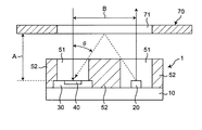
- the optical sensor 1 As shown in FIG. 1, the optical sensor 1 according to the first embodiment of the present invention includes a sensor substrate 10, and a light emitting element 20 and a light receiving unit 30 that are spaced apart from each other on the sensor substrate 10. Yes.
- the light emitting element 20 and the light receiving element 40 are sealed with a light transmitting resin 51.
- the area around the light emitting element 20 and the light receiving element 40 is sealed with a light shielding resin 52.
- the sensor substrate 10 is made of ceramics, for example, and a terminal 11 is provided on the bottom surface thereof. Ceramics has a property that it has a smaller coefficient of thermal expansion than a resin substrate and is less likely to warp.
- An etalon filter 60 of the light receiving element 40 to be described later may be broken by warping when a large stress is applied. For this reason, the etalon filter 60 is prevented from cracking by making the sensor substrate 10 a ceramic having a small thermal expansion coefficient and hardly warping.
- the light emitting element 20 is, for example, an LED or a laser having a wavelength region WR having a peak at 850 nm, and is connected to the sensor substrate 10 by wire bonding.
- the light receiving unit 30 is an LSI chip in which the light receiving element 40 is built, and is connected to the sensor substrate 10 by wire bonding.
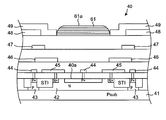
- the light receiving element 40 includes a semiconductor substrate 41, an N-type semiconductor layer 42 and a P-type semiconductor layer 43 provided on the semiconductor substrate 41, and an N-type semiconductor layer 42 and a P-type semiconductor layer 43.
- P + diffusion layer 44 for anode diffusion and N + diffusion layer 45 for cathode diffusion first to third conductive films 46 to 48 provided on P + diffusion layer 44 and N + diffusion layer 45, and 3 and a passivation film 49 provided on the conductive film 48.
- the semiconductor substrate 41 is, for example, a P-type (100) silicon substrate having a resistivity of 10 ⁇ ⁇ cm.
- the N-type semiconductor layer 42 is formed by ion-implanting 31P + (phosphorus) of about 1.0E + 13 cm ⁇ 3 at 150 keV and performing heat treatment by annealing at 900 ° C. Further, the P-type semiconductor layer 43 is formed by ion-implanting 11B + (boron) of about 1.0E + 13 cm ⁇ 3 at 250 keV and similarly heat-treating by annealing at 900 ° C. Note that the P-type semiconductor layer 43 is disposed so as to sandwich the N-type semiconductor layer 42.
- the P + diffusion layer 44 is formed by ion-implanting 11B + (boron) of about 2.0E + 15 cm ⁇ 3 at 30 keV and performing RTA (Rapid Thermal Anneal) at 1000 ° C. for 30 seconds.
- the N + diffusion layer 45 is formed by ion-implanting 31P + (phosphorus) of about 1.0E + 15 cm ⁇ 3 at 50 keV and similarly performing RTA at 1000 ° C. for 30 seconds.
- a PN junction is formed between the P + diffusion layer 44 and the N-type semiconductor layer 42 and functions as a photodiode.
- a region functioning as the photodiode is a light receiving surface 40a.
- a silicon oxide film (not shown) formed by a method such as thermal oxidation is provided between the P + diffusion layer 44 and the N + diffusion layer 45, and the N-type semiconductor layer 42 and the P-type semiconductor layer 43. ing.
- a silicon oxide film serving as a field film is formed by CVD (chemical vapor deposition), CMP (chemical mechanical polishing), or the like. Has been.
- the first conductive film 46 is made of AlCu with a thickness of 50 nm, is provided on the silicon oxide film on the P + diffusion layer 44 and the N + diffusion layer 45, and serves as an anode wiring and a cathode wiring.
- a silicon oxide film serving as an insulating film having a thickness of about 1000 nm is formed on the first conductive film 46 by CVD, CMP, or the like.
- the second conductive film 47 is made of AlCu having a thickness of about 500 nm, and is provided on the silicon oxide film on the first conductive film 46.
- a silicon oxide film serving as an insulating film having a thickness of about 1000 nm is formed on the second conductive film 47 by CVD, CMP, or the like.
- the third conductive film 48 is made of AlCu having a thickness of about 2 ⁇ m, and is provided on the silicon oxide film on the second conductive film 47.
- the third conductive film 48 functions as a light shielding film and is disposed so that light does not enter a region other than the region facing the light receiving surface 40 a of the light receiving element 40.
- the passivation film 49 is made of, for example, Si 3 N 4 and is provided on the silicon oxide film on the second conductive film 47 and on the third conductive film 48. An opening is provided in a region of the passivation film 49 facing the light receiving surface 40a. Since the refractive index (2) of Si 3 N 4 is higher than that of SiO 2 (1.46), the variation in reflectance can be reduced by providing an opening in a region facing the light receiving surface 40a.
- the light receiving element 40 includes an etalon filter 60 as an example of an incident light restricting unit.
- the etalon filter 60 is provided in a region facing the light receiving surface 40a on the silicon oxide film on the second conductive film 47, and its upper surface 60a is parallel to the light receiving surface 40a and covers the light receiving surface 40a. Is arranged.
- the etalon filter 60 includes a 30 nm metal film (Ag) and a 160 nm thick dielectric film (Si 3 N 4 ) sandwiched between the metal films.
- the etalon filter 60 is formed by forming a lift-off resist in a region other than the region facing the light receiving surface 40a, forming an Ag / Si 3 N 4 / Ag film by sputtering or vapor deposition, and then immersing it in a resist stripping solution. It is formed by removing the resist.
- the etalon filter 60 is a wavelength filter using multiple interference between two opposing reflecting surfaces.
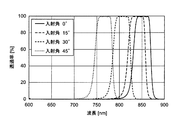
- the light incident on the etalon filter has a transmittance that varies depending on the incident angle ⁇ because the optical path length in the dielectric varies depending on the incident angle ⁇ (shown in FIG. 5).
- the incident angle ⁇ is 0 degree (direction perpendicular to the upper surface 60a of the etalon filter 60).
- the transmittance is highest when light having a wavelength of 850 nm is incident, and the transmittance is about 40%.
- the incident angle ⁇ is 15 degrees, the transmittance is highest when light having a wavelength of about 875 nm is incident, and the transmittance of light having a wavelength of 850 nm is about 16%.
- the transmittance When the incident angle ⁇ is 30 degrees, the transmittance is highest when light having a wavelength of about 950 nm is incident, and the transmittance of light having a wavelength of 850 nm is about 2%. When the incident angle ⁇ is 45 degrees, the transmittance is highest when light having a wavelength of about 1150 nm is incident, and the transmittance of light having a wavelength of 850 nm is approximately zero%.
- the incident angle ⁇ (hereinafter referred to as the regulation angle ⁇ 0 ) that can block the light incident on the light receiving element 40 is 45 degrees ( ⁇ ⁇ 0 ... light transmission, ⁇ ⁇ ⁇ 0 ... light blocking).
- the etalon filter 60 is provided in a state where the third conductive film 48 is not separated from the region facing the light receiving surface 40a by a certain distance, the etalon filter 60 is distorted. For this reason, it is preferable that the third conductive film 48 be disposed at least by the thickness of the interference film from the boundary of the region facing the light receiving surface 40a.
- the optical sensor 1 is arranged so that the light emitting element 20 and the light receiving element 40 face the transparent casing window 71 inside the housing 70 of the electronic device. Be placed.
- the light emitted from the light emitting element 20 of the optical sensor 1 and reflected by the object to be detected forms an angle of approximately 90 degrees ( ⁇ 0) with respect to the light receiving surface 40a of the light receiving element 40, and enters the light receiving element 40.
- ⁇ 0 degrees
- a part of the light emitted from the side of the light emitting element 20 hits the casing 70 instead of the object to be detected and is reflected toward the light receiving element 40.
- a gap between the upper surface of the optical sensor 1 and the housing 70 is provided between the light emitting element 20 and the light receiving element 40.
- a method of providing a rubber cap 80 for closing is conceivable.
- the rubber cap 80 since the distance between the optical sensor 1 and the housing 70 differs depending on the type of the electronic device, the rubber cap 80 must be designed for each mounted model, and the rubber cap 80 is provided. Therefore, the manufacturing cost is increased.
- the optical sensor 1 of the first embodiment among the light emitted from the light emitting element 20 incident on the light receiving element 40, light having an incident angle ⁇ of not more than the regulation angle ⁇ 0 is transmitted through the etalon filter 60 and the regulation angle ⁇ 0. The above light is blocked by the etalon filter 60.
- the transmittance is about 40%, and the light reflected by the object to be detected is transmitted through the etalon filter 60 to the light receiving surface 40a.
- the transmittance is much lower than 5% at all wavelengths of the laser (about 820 to 880 nm), and particularly at the laser peak wavelength of 850 nm, the transmittance is almost zero. It has become. For this reason, the light of the wavelength of all the bands reflected by the housing 70 is interrupted
- the optical sensor 1 even when the light emitting element 20 that emits light having a wavelength in a predetermined band such as a laser is used, the light is emitted from the light emitting element 20 toward the light receiving element 40 without being reflected by the object to be detected. It is possible to reduce the intensity of light of all the band wavelengths. As a result, it is possible to detect information related to the detected object with high accuracy.
- the etalon filter 60 is used as the incident light restricting portion.
- the incident light restricting portion can be made thin to eliminate problems such as warping, and the cost can be reduced.
- the etalon filter 60 is designed so as to block the primary reflected light toward the light receiving element without being reflected by the object to be detected, so that the detection accuracy can be improved efficiently. Can do.
- the restriction angle ⁇ 0 is calculated by the following equation.
- A is the distance between the surfaces of the light receiving element 40 and the housing 70
- B is the distance between the centers of the light emitting element 20 and the light receiving element 40.
- ⁇ 0 tan ⁇ 1 (B / A)
- the optical sensor 1 according to the second embodiment of the present invention is the same as that of the first embodiment in that a dielectric multilayer film 61 in which a plurality of dielectric films are stacked is provided as an incident light restricting portion. Different from the optical sensor 1.
- the dielectric multilayer film 61 is composed of 40 layers of dielectric films (Nb 2 O 3 / SiO 2 ).
- a lift-off resist is formed in a region other than the region facing the light receiving surface 40a, a dielectric film is formed by sputtering or vapor deposition, and then the resist is removed by immersion in a resist stripping solution. Is formed.
- the 40-layer dielectric films have different thicknesses and are designed to have a transmission region at 850 nm.
- the dielectric multilayer film 61 is a band-pass filter that transmits only light in a specific band by stacking a plurality of dielectric films such as metal oxide films.
- the light incident on the dielectric multilayer film 61 varies in optical transmittance according to the incident angle ⁇ because the optical path length in each dielectric varies depending on the incident angle ⁇ .
- the incident angle ⁇ is 0 degree (the upper surface 61a of the dielectric multilayer film 61 (shown in FIG. 7)).
- the transmittance is highest when light having a wavelength of about 880 nm is incident, and the transmittance of light having a wavelength of 850 nm is about 95%.
- the incident angle ⁇ is 15 degrees, the transmittance is highest when light having a wavelength of about 870 nm is incident, and the transmittance of light having a wavelength of 850 nm is about 97%.
- the transmittance When the incident angle ⁇ is 30 degrees, the transmittance is highest when light having a wavelength of about 820 nm is incident, and the transmittance of light having a wavelength of 850 nm is about 95%. When the incident angle ⁇ is 45 degrees, the transmittance is highest when light having a wavelength of about 780 nm is incident, and the transmittance of light having a wavelength of 850 nm is about 10%.
- the restriction angle ⁇ 0 is 45 degrees ( ⁇ ⁇ 0 ... light transmission, ⁇ ⁇ ⁇ 0 ... light blocking).
- the cutoff waveform can be designed sharply, and the S / N ratio of the sensor can be improved because the cutoff wavelength and the transmission wavelength can be clearly distinguished.
- the dielectric film of the dielectric multilayer film 61 is not limited to Nb 2 O 3 / SiO 2 , but can be appropriately selected from TiO 2, Si 3 N 4, or the like according to the design of the transmission region.
- An avalanche photodiode may be used as the light receiving element 40.
- an avalanche photodiode with high light receiving sensitivity as the light receiving element 40, detection accuracy can be increased.
- the optical sensor 1 is characterized in that it includes an incident light restricting section that transmits light having a small incident angle ⁇ and blocks light having a large incident angle ⁇ . It goes without saying that it is good.
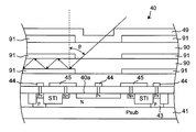
- a dielectric film 90 provided with a light pocket for guiding light having a predetermined incident angle ⁇ or more on the side surface, and a metal covering the upper and lower surfaces of the dielectric film 90
- a filter composed of the film 91 may be used as an incident light restricting portion.
- This filter is configured such that light incident at a predetermined incident angle ⁇ enters between the metal films 91 and does not return.
- the optical sensor 1 can be made into a structure that blocks light larger than the predetermined incident angle ⁇ and does not consider it as light sensitivity.
- glass or a film is disposed between objects such as a TOF sensor using a laser and a proximity sensor / photointerrupter / original size sensor using an LED.
- the present invention can be applied to a reflective optical sensor.
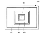
- the light receiving element 40 includes a sensor unit 401, a first circuit unit 402, and a second circuit unit 403, and serves as an incident light regulating unit.
- the inorganic film filter 62 is different from the optical sensor 1 of the first embodiment in that the inorganic film filter 62 is disposed so as to cover the sensor unit 401, the first circuit unit 402, and the second circuit unit 403.
- the sensor unit 401 includes a semiconductor substrate 41, an N-type semiconductor layer 42 and a P-type semiconductor layer 43 provided on the semiconductor substrate 41, and an anode diffusion provided on the N-type semiconductor layer 42 and the P-type semiconductor layer 43.
- P + diffusion layer 44 to be formed P + diffusion layer 44 to be formed, N + diffusion layer 45 to be cathode diffusion, first to third conductive films 46 to 48 provided on P + diffusion layer 44 and N + diffusion layer 45, and provided on third conductive film 48 And a light-receiving surface 40a.
- Each of the first circuit portion 402 and the second circuit portion 403 is formed by a semiconductor process using silicon.
- the first circuit unit 402 is arranged around a virtual straight line orthogonal to the light receiving surface 40 a of the sensor unit 401 and on the outer periphery of the sensor unit 401 with a gap from the sensor unit 401.
- the second circuit unit 403 is disposed around the virtual straight line orthogonal to the light receiving surface 40 a of the sensor unit 401 and on the outer periphery of the first circuit unit 402 with a space from the first circuit unit 402.
- the inorganic film filter 62 is made of, for example, SiO 2 / Nb 2 O 2 or SiO 2 / Ag, and has a substantially rectangular shape in plan view along a direction orthogonal to the light receiving surface 40 a of the sensor unit 401. .
- the inorganic film filter 62 covers substantially the entire surface of the light receiving element 40 excluding an electrode section (not shown) called a PAD section, that is, the sensor section 401, the first circuit section 402, and the second circuit section. It is provided so as to cover the entire surface of 403.
- the inorganic film filter 62 made of SiO 2 / Nb 2 O 2 or SiO 2 / Ag and the first circuit part 402 and the second circuit part 403 made of silicon have different thermal expansion coefficients. Therefore, as shown in FIG. 12, when the inorganic film filter 62 covers only the sensor unit 401 and the vicinity thereof without covering the first circuit unit 402 and the second circuit unit 403 of the light receiving element 40, the following problem occurs. May occur.
- the first circuit unit 402 and the second circuit unit 403 are also covered with the inorganic film filter 62. Therefore, the first circuit unit 402 and the second circuit unit The influence of the stress by the inorganic film filter 62 on 403 is reduced, and the difference between the characteristics of the region covered with the inorganic film filter 62 and the characteristics of the region not covered with the inorganic film filter 62 in the light receiving element 40 is obtained. Can be reduced.
- the lift-off resist area can be reduced, degas from the resist can be minimized and a stable film quality can be obtained. As a result, the most important angle dependence can be maintained.
- the first circuit unit 402 and the second circuit unit 403 are provided as circuit units, but the present invention is not limited to this.
- the configuration of the circuit unit such as the material, size, range, and number, can be changed as appropriate according to the design of the optical sensor 1 and the like.
- the optical sensor 1 according to the seventh embodiment of the present invention is the sixth embodiment in that the incident light restricting portion includes a plurality of inorganic film filters 63 as an example of a plurality of filters. This is different from the optical sensor 1 of FIG.
- the incident light restricting portion is composed of 21 inorganic film filters 63 having substantially the same size.
- Each inorganic membrane filter 63 is made of, for example, Ag / Nb 2 O 3 and has a substantially rectangular shape in plan view along a direction orthogonal to the light receiving surface 40a of the sensor unit 401.
- the size of each inorganic membrane filter 63 is smaller than that of the inorganic membrane filter 62 of the sixth embodiment.
- the inorganic film filters 63 are arranged so as to cover substantially the entire surface of the sensor unit 401, the first circuit unit 402, and the second circuit unit 403 at an interval so as not to overlap each other.
- the inorganic film filter 62 when the inorganic film filter 62 is disposed so as to cover the entire surface of the sensor unit 401, the first circuit unit 402, and the second circuit unit 403 of the light receiving element 40 as in the optical sensor 1 of the sixth embodiment,
- the heat treatment in the reflow process when mounting the light receiving element 40 may cause a problem that internal stress is generated in the incident light restricting portion (that is, the inorganic film filter 62) and the inorganic film filter 62 is broken.
- the plurality of inorganic film filters 63 are arranged at intervals so as not to overlap each other, and as a whole, the sensor unit 401, the first circuit unit 402, and the second circuit unit 403 are arranged. It covers almost the entire surface. Thereby, in the reflow process when mounting the light receiving element 40 while covering the substantially entire surface of the sensor unit 401, the first circuit unit 402, and the second circuit unit 403 of the light receiving element 40 by the plurality of inorganic film filters 63.
- the internal stress generated in the incident light restricting portion that is, each inorganic film filter 63
- each inorganic membrane filter 63 can be arbitrarily set. However, by making all the inorganic membrane filters 63 the same size, the inorganic membrane filter 63 can be used for the first circuit portion 402 and the second circuit portion 403. Stress can be reduced.
- the optical sensor 1 of the present invention includes: A light emitting element 20 for irradiating the detection object with light; A light receiving element 40 having a light receiving surface 40a for receiving light emitted from the light emitting element 20, and With Incident light restricting portions 60 and 61 covering the light receiving surface 40a are provided on the path of the light emitted from the light emitting element 20 toward the light receiving surface 40a.
- the incident light restricting sections 60 and 61 transmit light having the incident angle ⁇ less than a predetermined value among light incident on the light receiving element 20 and block light having the incident angle ⁇ equal to or larger than the predetermined value. It is characterized by that.
- the light reception on the light receiving surface 40a is regulated according to the incident angle ⁇ of the light emitted from the light emitting element 20 incident on the light receiving element 40.
- the incident angle ⁇ of the light emitted from the light emitting element 20 incident on the light receiving element 40 For example, light having a wavelength in a predetermined band Even when the light emitting element 20 that emits light is used, the intensity of light emitted from the light emitting element 20 and directed toward the light receiving surface 40a without being reflected by the object to be detected can be reduced. As a result, it is possible to detect information related to the detected object with high accuracy.
- the incident light restricting portion is the etalon filter 60.
- the incident light restricting portion is a dielectric multilayer film 61 in which a plurality of dielectric films are laminated.
- the cutoff waveform can be designed steeply, and the S / N ratio of the sensor can be improved because the cutoff wavelength and the transmission wavelength can be clearly distinguished.
- the light receiving element 40 is A sensor unit 401 having the light receiving surface 40a; Circuit portions 402 and 403 disposed around the sensor portion 401, The incident light restricting portion is disposed so as to cover the sensor portion and the circuit portion.
- the influence of the stress by the incident light restricting portion 62 on the circuit portions 402 and 403 is reduced, and the characteristics of the region covered with the incident light restricting portion 62 in the light receiving element 40 and the incident light restricting portion 62 are determined.
- the difference between the characteristics of the region not covered with can be reduced.
- the said incident light control part is comprised with the some filter arrange
- the plurality of filters 63 cover the sensor unit 401 and the circuit units 402 and 403 of the light receiving element 40, and are generated in each filter 63 by heat treatment in a reflow process when mounting the light receiving element 40, for example. Therefore, the occurrence of problems such as breakage of the inorganic film filter 62 can be avoided.
- the light emitting element 20 is a laser.
- the detection accuracy can be improved efficiently by designing the incident light restricting portions 60 and 61 so that the primary reflected light directed to the light receiving element 40 without being reflected by the detection object can be blocked. .
Landscapes
- Physics & Mathematics (AREA)
- Engineering & Computer Science (AREA)
- General Physics & Mathematics (AREA)
- Electromagnetism (AREA)
- Spectroscopy & Molecular Physics (AREA)
- Optics & Photonics (AREA)
- Computer Networks & Wireless Communication (AREA)
- Radar, Positioning & Navigation (AREA)
- Remote Sensing (AREA)
- Light Receiving Elements (AREA)
- Photo Coupler, Interrupter, Optical-To-Optical Conversion Devices (AREA)
- Microelectronics & Electronic Packaging (AREA)
Abstract
La présente invention a trait à un photodétecteur (1), lequel photodétecteur comporte : un élément émetteur de lumière (20) qui émet de la lumière vers un objet à détecter ; et un élément récepteur de lumière (40) qui présente une surface de réception de lumière (40a) qui reçoit la lumière rayonnée à partir de l'élément émetteur de lumière (20). Une partie régulation de la lumière incidente (60), qui recouvre la surface de réception de lumière (40a), est placée sur un trajet de la lumière où la lumière rayonnée à partir de l'élément émetteur de lumière (20) se déplace vers la surface réceptrice de la lumière (40a) ; et la partie régulation de lumière incidente (60) transmet la lumière qui présente un angle d'incidence inférieur à une valeur prédéfinie au sein de la lumière incidente sur l'élément récepteur de lumière (40), tout en bloquant la lumière qui présente un angle d'incidence supérieur ou égal à la valeur prédéfinie.
Priority Applications (2)
| Application Number | Priority Date | Filing Date | Title |
|---|---|---|---|
| US16/304,284 US10566489B2 (en) | 2016-05-26 | 2017-05-26 | Photosensor |
| CN201780032650.6A CN109196663B (zh) | 2016-05-26 | 2017-05-26 | 光传感器 |
Applications Claiming Priority (2)
| Application Number | Priority Date | Filing Date | Title |
|---|---|---|---|
| JP2016-104944 | 2016-05-26 | ||
| JP2016104944A JP2019133960A (ja) | 2016-05-26 | 2016-05-26 | 光センサ |
Publications (1)
| Publication Number | Publication Date |
|---|---|
| WO2017204331A1 true WO2017204331A1 (fr) | 2017-11-30 |
Family
ID=60412741
Family Applications (1)
| Application Number | Title | Priority Date | Filing Date |
|---|---|---|---|
| PCT/JP2017/019698 Ceased WO2017204331A1 (fr) | 2016-05-26 | 2017-05-26 | Photodétecteur |
Country Status (4)
| Country | Link |
|---|---|
| US (1) | US10566489B2 (fr) |
| JP (1) | JP2019133960A (fr) |
| CN (1) | CN109196663B (fr) |
| WO (1) | WO2017204331A1 (fr) |
Families Citing this family (2)
| Publication number | Priority date | Publication date | Assignee | Title |
|---|---|---|---|---|
| CN112998680B (zh) * | 2021-02-23 | 2023-03-21 | 潍坊歌尔微电子有限公司 | 测试机构 |
| CN116613622B (zh) * | 2023-07-19 | 2024-04-05 | 青岛泰睿思微电子有限公司 | 双凹槽光传感器封装结构 |
Citations (4)
| Publication number | Priority date | Publication date | Assignee | Title |
|---|---|---|---|---|
| JP2005175256A (ja) * | 2003-12-12 | 2005-06-30 | Konica Minolta Holdings Inc | 受光装置及び投受光装置 |
| JP2006040913A (ja) * | 2004-07-22 | 2006-02-09 | Takenaka Electronic Industrial Co Ltd | 光電センサ |
| JP2010258350A (ja) * | 2009-04-28 | 2010-11-11 | Sanyo Electric Co Ltd | 発光装置、情報取得装置および物体検出装置 |
| US20130327931A1 (en) * | 2012-06-06 | 2013-12-12 | Pixart Imaging Incorporation | Package structure of optical apparatus |
Family Cites Families (8)
| Publication number | Priority date | Publication date | Assignee | Title |
|---|---|---|---|---|
| JP2006072171A (ja) * | 2004-09-06 | 2006-03-16 | Hitachi Ltd | 光モジュール |
| KR101391792B1 (ko) * | 2008-01-04 | 2014-05-07 | 삼성전자주식회사 | 화상독취장치 및 이를 갖춘 화상형성기기 |
| JP2011049473A (ja) | 2009-08-28 | 2011-03-10 | Sharp Corp | 光検出装置および電子機器 |
| JP5810565B2 (ja) * | 2011-03-16 | 2015-11-11 | セイコーエプソン株式会社 | 光学センサー及び電子機器 |
| CN107369728B (zh) * | 2012-08-30 | 2019-07-26 | 京瓷株式会社 | 受光发光元件以及使用该受光发光元件的传感器装置 |
| CN103926629B (zh) * | 2013-01-11 | 2017-03-08 | 原相科技股份有限公司 | 光学装置、使用微透镜的感光元件及其制作方法 |
| CN105465656A (zh) * | 2014-08-29 | 2016-04-06 | 陈雁北 | 一种发光装置 |
| CN108289618A (zh) * | 2015-11-30 | 2018-07-17 | 新日本无线株式会社 | 光电传感器 |
-
2016
- 2016-05-26 JP JP2016104944A patent/JP2019133960A/ja active Pending
-
2017
- 2017-05-26 CN CN201780032650.6A patent/CN109196663B/zh active Active
- 2017-05-26 US US16/304,284 patent/US10566489B2/en active Active
- 2017-05-26 WO PCT/JP2017/019698 patent/WO2017204331A1/fr not_active Ceased
Patent Citations (4)
| Publication number | Priority date | Publication date | Assignee | Title |
|---|---|---|---|---|
| JP2005175256A (ja) * | 2003-12-12 | 2005-06-30 | Konica Minolta Holdings Inc | 受光装置及び投受光装置 |
| JP2006040913A (ja) * | 2004-07-22 | 2006-02-09 | Takenaka Electronic Industrial Co Ltd | 光電センサ |
| JP2010258350A (ja) * | 2009-04-28 | 2010-11-11 | Sanyo Electric Co Ltd | 発光装置、情報取得装置および物体検出装置 |
| US20130327931A1 (en) * | 2012-06-06 | 2013-12-12 | Pixart Imaging Incorporation | Package structure of optical apparatus |
Also Published As
| Publication number | Publication date |
|---|---|
| CN109196663B (zh) | 2022-03-22 |
| JP2019133960A (ja) | 2019-08-08 |
| US10566489B2 (en) | 2020-02-18 |
| US20190109255A1 (en) | 2019-04-11 |
| CN109196663A (zh) | 2019-01-11 |
Similar Documents
| Publication | Publication Date | Title |
|---|---|---|
| EP2180509A1 (fr) | Capteur de lumière | |
| CN108140125B (zh) | 光学指纹成像系统和面阵传感器 | |
| JP5988690B2 (ja) | 分光センサ | |
| CN113358223B (zh) | 光检测装置 | |
| CN104272070B (zh) | 分光传感器 | |
| CN105679842A (zh) | 光电转换装置及电子设备 | |
| JP5875936B2 (ja) | 分光センサ | |
| JP5670360B2 (ja) | 半導体受光素子及びオプトエレクトロニクス装置 | |
| US10566489B2 (en) | Photosensor | |
| JP5821400B2 (ja) | 分光センサー及び角度制限フィルター | |
| JP5375840B2 (ja) | 光センサ | |
| JP6654067B2 (ja) | 光センサ | |
| JP6079840B2 (ja) | 分光センサー及び角度制限フィルター | |
| JP5402893B2 (ja) | 光センサ | |
| JP6160167B2 (ja) | 分光センサー及びその製造方法 | |
| JP6191196B2 (ja) | 分光センサー及びその製造方法 | |
| JP2012194438A (ja) | 分光センサー及び角度制限フィルター | |
| JP2009076790A (ja) | 紫外線センサ、紫外線センサの設定方法 | |
| WO2017094278A1 (fr) | Photodétecteur | |
| JP5804166B2 (ja) | 分光センサー及び角度制限フィルター | |
| US9947814B2 (en) | Semiconductor optical sensor |
Legal Events
| Date | Code | Title | Description |
|---|---|---|---|
| DPE2 | Request for preliminary examination filed before expiration of 19th month from priority date (pct application filed from 20040101) | ||
| NENP | Non-entry into the national phase |
Ref country code: DE |
|
| 121 | Ep: the epo has been informed by wipo that ep was designated in this application |
Ref document number: 17802917 Country of ref document: EP Kind code of ref document: A1 |
|
| 122 | Ep: pct application non-entry in european phase |
Ref document number: 17802917 Country of ref document: EP Kind code of ref document: A1 |
|
| NENP | Non-entry into the national phase |
Ref country code: JP |