WO2017208382A1 - Déphaseur, dispositif de distribution/synthèse, antenne réseau et antenne sectorielle - Google Patents
Déphaseur, dispositif de distribution/synthèse, antenne réseau et antenne sectorielle Download PDFInfo
- Publication number
- WO2017208382A1 WO2017208382A1 PCT/JP2016/066138 JP2016066138W WO2017208382A1 WO 2017208382 A1 WO2017208382 A1 WO 2017208382A1 JP 2016066138 W JP2016066138 W JP 2016066138W WO 2017208382 A1 WO2017208382 A1 WO 2017208382A1
- Authority
- WO
- WIPO (PCT)
- Prior art keywords
- line
- conductor
- line conductor
- substrate
- phase shifter
- Prior art date
- Legal status (The legal status is an assumption and is not a legal conclusion. Google has not performed a legal analysis and makes no representation as to the accuracy of the status listed.)
- Ceased
Links
Images









Classifications
-
- H—ELECTRICITY
- H01—ELECTRIC ELEMENTS
- H01P—WAVEGUIDES; RESONATORS, LINES, OR OTHER DEVICES OF THE WAVEGUIDE TYPE
- H01P1/00—Auxiliary devices
- H01P1/18—Phase-shifters
-
- H—ELECTRICITY
- H01—ELECTRIC ELEMENTS
- H01Q—ANTENNAS, i.e. RADIO AERIALS
- H01Q1/00—Details of, or arrangements associated with, antennas
- H01Q1/36—Structural form of radiating elements, e.g. cone, spiral, umbrella; Particular materials used therewith
-
- H—ELECTRICITY
- H01—ELECTRIC ELEMENTS
- H01Q—ANTENNAS, i.e. RADIO AERIALS
- H01Q1/00—Details of, or arrangements associated with, antennas
- H01Q1/42—Housings not intimately mechanically associated with radiating elements, e.g. radome
-
- H—ELECTRICITY
- H01—ELECTRIC ELEMENTS
- H01Q—ANTENNAS, i.e. RADIO AERIALS
- H01Q15/00—Devices for reflection, refraction, diffraction or polarisation of waves radiated from an antenna, e.g. quasi-optical devices
- H01Q15/14—Reflecting surfaces; Equivalent structures
-
- H—ELECTRICITY
- H01—ELECTRIC ELEMENTS
- H01Q—ANTENNAS, i.e. RADIO AERIALS
- H01Q3/00—Arrangements for changing or varying the orientation or the shape of the directional pattern of the waves radiated from an antenna or antenna system
- H01Q3/26—Arrangements for changing or varying the orientation or the shape of the directional pattern of the waves radiated from an antenna or antenna system varying the relative phase or relative amplitude of energisation between two or more active radiating elements; varying the distribution of energy across a radiating aperture
- H01Q3/30—Arrangements for changing or varying the orientation or the shape of the directional pattern of the waves radiated from an antenna or antenna system varying the relative phase or relative amplitude of energisation between two or more active radiating elements; varying the distribution of energy across a radiating aperture varying the relative phase between the radiating elements of an array
Definitions
- the present invention relates to a phase shifter, a distribution / synthesis device, an array antenna, and a sector antenna.
- a base station antenna for mobile communication As a base station antenna for mobile communication, a plurality of sector antennas that radiate radio waves for each sector (area) set corresponding to the direction in which radio waves are radiated are used in combination.
- the sector antenna an array antenna in which radiating elements (antennas) such as a dipole antenna are arranged in an array is used. And the directivity of the array antenna is set by controlling the phase of the input signal supplied to each antenna element of the array antenna or the output signal received by each antenna element by the phase shifter.
- Patent Document 1 a main substrate on which a plurality of pairs of microstrip lines are formed, a dielectric substrate movable with respect to the main substrate, and the microstrip of the main substrate formed on the surface of the dielectric substrate.
- a phase shifter is described in which a microstrip line and the coupling microstrip line of the passage plate face each other so as to overlap each other.
- Patent Document 2 discloses a housing having a rectangular box shape with a long plane, a portion of a plurality of phase variable patterns attached to the bottom surface of the housing, for distributing an input signal and for varying the phase of the distributed signal, and A fixed board on which transmission lines forming a plurality of signal distribution patterns are printed, and a position in contact with one surface of the fixed board in the housing so as to be movable along a length direction; A movable substrate on which a transmission line is printed to form a variable line via coupling with a part of the phase variable pattern to form a remaining part of the plurality of phase variable patterns for phase variable A multiline phase shifter for a beam tilt control antenna is described.
- Patent Document 3 a first conductor and a second conductor arranged in parallel with an interval of less than 1 ⁇ 4 of the wavelength of the high-frequency signal and fixed, and the first conductor and the second conductor are capacitively coupled. And a movable conductor capable of reciprocating in the longitudinal direction of the first conductor and the second conductor, and the movable conductor is overlapped with one longitudinal end of the first conductor. An output portion that overlaps the longitudinal intermediate portion of the second conducting wire, and a connecting portion that connects the input portion and the output portion, wherein the movable conductor is between the first conducting wire and the second conducting wire.
- a distribution phase shifter that forms a line having a length of 1/4 or more of the wavelength of the high-frequency signal is described.
- Patent Document 4 includes an antenna feed line, and a first ground layer and a second ground layer that are spaced apart from the antenna feed line so as to sandwich the antenna feed line therebetween.
- the first grounding layer is formed in a predetermined shape, so that the antenna triplate line that functions as an antenna element capable of transmitting and receiving electromagnetic waves, the second grounding layer, and the second grounding layer are separated to the lower layer side.
- a routing power supply line, and a third grounding layer disposed so as to be spaced apart from the routing power supply line so as to sandwich the routing power supply line between the second grounding layer and the routing power supply line.
- an antenna device including a plate line, in which an antenna feed line and a routing feed line are electrically connected outside the edge of the second ground layer.
- JP 2012-39297 A Special table 2012-526447 gazette JP 2014-72625 A JP2015-91059A
- a sector antenna used for a base station antenna for mobile communication is required to have a wide band in addition to downsizing and the like.
- An object of the present invention is to provide a phase shifter and the like that can increase the bandwidth while miniaturizing a sector antenna.
- the phase shifter to which the present invention is applied includes at least one reference conductor to which a reference potential is supplied, a transmission path that faces the reference conductor, and a first signal to which a signal is input.
- a line conductor, a second line conductor that is provided on the first line conductor side forms a transmission path opposite to the reference conductor, and outputs a signal, and the first line conductor and the second line conductor
- a third line conductor that forms a transmission line facing the reference conductor, and is electrically coupled in a relatively movable state, and includes a first line conductor, a second line conductor, and a second line conductor
- the characteristic impedance has a portion different from the other portions.
- a part having a different characteristic impedance from another part has a different width. be able to.
- the characteristic impedance is different from the other parts because the first line conductor and the third line conductor face each other and are electrically coupled, and the second line conductor and the third line conductor.
- the reference conductor is provided on one surface of a plate made of a dielectric, and the first line conductor and the second line conductor are provided on the other surface of the plate made of a dielectric.
- the phase shifter to which the present invention is applied has a reference conductor to which a reference potential is supplied provided on one surface, and a first line conductor to which a signal is input and a signal is output.
- the second line conductor is electrically movable in a relatively movable state with respect to the first substrate made of a dielectric provided on the other surface, and the first line conductor and the second line conductor.
- a second substrate composed of a dielectric provided on one surface with a third line conductor coupled to the reference conductor and forming a transmission line facing the reference conductor; and a third line conductor of the second substrate
- a pressing member that presses the surface provided with the first line conductor and the second line conductor of the first substrate, and covers the pressing member and the second substrate from the holding member side, A covering member fixed to the first substrate.
- the pressing member may be provided with a spring portion having a protrusion on the second substrate side so as to contact and hold the second substrate.
- the pressing member may include a spring portion having a protrusion that contacts the upper surface of the covering member and presses the pressing member against the covering member.
- the pressing member may be provided with a convex portion that restrains the second substrate by being inserted into a through-hole provided in the second substrate.
- the covering member includes a plurality of convex portions that are inserted into a through hole provided in the first substrate and fixed to the first substrate by a barb provided at the tip around the covering member. Can be a feature.
- the distribution / synthesis device to which the present invention is applied includes at least one reference conductor to which a reference potential is supplied, a transmission path that faces the reference conductor, and a signal is input.
- the first line conductor is configured to be opposed to the reference conductor, the second line conductor from which a signal is output, and the first line conductor and the second line conductor are movable relative to each other.
- a plurality of phase shifters including a third line conductor that forms a transmission path opposite to the reference conductor and either directly or via a plurality of phase shifters And a distribution / combination line for distributing signals to a plurality of connected antennas or synthesizing signals from the plurality of antennas.
- the phase shifter has a characteristic impedance difference between at least one of the first line conductor, the second line conductor, and the third line conductor.
- it can be characterized by including a phase shift amount setting unit that sets at least one phase shifter of the plurality of phase shifters and at least one other phase shifter to different phase shift amounts.
- the phase shift amount setting unit is provided to be connected to the first male screw part having the first pitch and the same shaft as the first male screw part, and has a second pitch different from the first pitch.
- a second male screw portion, and at least one of the plurality of phase shifters meshes with the first male screw portion fitted into the first male screw portion by rotation of the shaft.
- the first phase shift amount is set by the movement of the first moving member having one female threaded portion, and at least one other phase shifter among the plurality of phase shifters is moved to the second phase by the rotation of the shaft.
- a second phase shift amount different from the first phase shift amount is set by movement of a second transition member having a second female screw portion engaged with the second male screw portion and fitted into the male screw portion. It can be.
- the array antenna to which the present invention is applied has a reference conductor to which a reference potential is supplied provided on one surface, and a first line conductor to which a signal is input and a signal are output.
- the second line conductor is electrically coupled to the first substrate made of a dielectric provided on the other surface and movable relative to the first line conductor and the second line conductor.
- a second substrate made of a dielectric provided on one surface with a third line conductor forming a transmission line facing the reference conductor, and a plurality of phase shifters,
- the radiation element and the other surface of the first substrate are provided either directly or via a plurality of phase shifters, and distribute signals to the plurality of radiation elements or synthesize signals from the plurality of radiation elements.
- the phase shifter includes a first line conductor and a second line conductor. In at least one and the third line conductor, the characteristic impedance and having different portions from the other portions.
- the sector antenna to which the present invention is applied has a reference conductor to which a reference potential is supplied provided on one surface, and a first line conductor to which a signal is input and a signal to be output.
- the second line conductor is electrically movable in a relatively movable state with respect to the first substrate made of a dielectric provided on the other surface, and the first line conductor and the second line conductor.
- a plurality of phase shifters comprising: a second substrate made of a dielectric having a third line conductor formed on one surface thereof, the third line conductor being coupled to and forming a transmission line facing the reference conductor; A plurality of radiating elements arranged at a predetermined interval on one surface of one substrate and provided on the other surface of the first substrate either directly or via a plurality of phase shifters; Distributing / combining signals to multiple radiating elements or combining signals from multiple radiating elements
- the characteristic impedance is different from the other parts.
- Such a sector antenna includes a phase shift amount setting unit that sets at least one phase shifter of a plurality of phase shifters and at least one other phase shifter to different phase shift amounts. can do.
- a phase shifter or the like that can increase the bandwidth can be provided.
- FIG. 1 It is a figure which shows an example of the whole structure of the base station antenna of the mobile communication with which 1st Embodiment is applied.
- A is a perspective view of a base station antenna
- (b) is a figure explaining the example of installation of a base station antenna. It is a perspective view of the array antenna in a 1st embodiment. It is a figure explaining a distribution circuit.
- (A) is a top view of a distribution circuit
- (b) is a figure explaining the relationship between the signal transmitted to an antenna, and a phase shifter. It is a figure explaining a phase shifter.
- (A) is a figure explaining the fixed line provided in the fixed board
- (b) is a figure explaining the movable line provided in the movable board
- (c) is ( It is a top view of the phase shifter which combined the fixed line and movable line of a). It is an enlarged view of the fixed line provided in the fixed board
- (A) shows a movable line
- (b) shows a fixed line
- and (c) shows the return loss characteristic of the phase shifter.
- FIG. 5 It is an enlarged view of the fixed line provided in the fixed board
- (A) shows a movable line
- (b) shows a fixed line
- (A) is a plan view seen from the movable line side
- (b) is a plan view seen from the fixed line side
- and (c) is a cross-sectional view taken along the VIIC-VIIC line of (a) and (b). is there.
- (A) is a plan view seen from the movable line side
- (b) is a plan view seen from the fixed line side
- (c) shows a return loss characteristic of the phase shifter.
- (A) is a plan view seen from the movable line side
- (b) is a plan view seen from the fixed line side
- (c) shows a return loss characteristic of the phase shifter.
- (A) is a plan view seen from the movable line side
- (b) is a plan view seen from the fixed line side
- (c) shows a return loss characteristic of the phase shifter.
- (A) is a plan view seen from the movable line side
- (b) is a plan view seen from the fixed line side
- (c) shows a return loss characteristic of the phase shifter. It is a figure explaining the holding mechanism holding a movable substrate in a phase shifter.
- (A) is a perspective view of a phase shifter provided with a holding mechanism
- (b) is a top view of the phase shifter viewed from the XI direction of (a). It is sectional drawing explaining the holding mechanism which hold
- (A) is a figure which shows the state which has arrange
- (b) is a figure which shows the state which fixed the fixed board
- FIG. 1 is a diagram illustrating an example of the overall configuration of a base station antenna 1 for mobile communication to which the first embodiment is applied.
- FIG. 1A is a perspective view of the base station antenna 1
- FIG. 1B is a diagram illustrating an installation example of the base station antenna 1.
- FIG. 1B is a view of the base station antenna 1 as viewed from above. As shown in FIG.
- the base station antenna 1 includes, for example, a plurality of sector antennas 10-1 to 10-3 (indicated as sector antennas 10 if not distinguished) held by a tower 20. .
- Each of the sector antennas 10-1 to 10-3 includes an array antenna 30.
- the array antenna 30 is covered with a radome 12 that protects against wind and rain.
- the radome 12 includes a cylindrical pipe, an upper lid that covers the upper surface, and a lower lid that covers the lower surface. That is, the outside of the sector antennas 10-1 to 10-3 is a radome 12, and the array antenna 30 is housed inside the radome 12.
- the radome 12 has a cylindrical shape, but may have other shapes.
- the radome 12 is made of a material having a low dielectric constant and a low dielectric loss tangent, such as resin and FRP (fiber reinforced plastic), which easily transmits radio waves.
- Each sector antenna 10 is connected to one end of transmission / reception cables 14 and 15 that transmit transmission signals and reception signals to the array antenna 30.
- the other ends of the transmission / reception cables 14 and 15 are connected to a transmission / reception unit (not shown) provided in a base station (not shown) for generating a transmission signal and receiving a reception signal.
- the transmission / reception cables 14 and 15 are, for example, coaxial cables. In FIG. 1A, the transmission / reception cables 14 and 15 are shown only for the sector antenna 10-1, but the other sector antennas 10-2 and 10-3 are also used for the transmission / reception cable 14 like the sector antenna 10-1. , 15.
- the transmission / reception cables 14 and 15 transmit signals of + 45 ° polarization and ⁇ 45 ° polarization, respectively (see FIG. 2).
- the sector antenna 10 is provided in the vertical direction. It may be provided obliquely from the vertical direction.
- the base station antenna 1, the sector antenna 10, the array antenna 30 and the like can transmit and receive radio waves due to the reversibility of the antenna. In the following, the case of transmitting radio waves will be described, but in the case of reception, the signal flow direction may be reversed.
- the base station antenna 1 transmits radio waves in the cell 2.
- Cell 2 is divided into a plurality of sectors 3-1 to 3-3 (indicated as sector 3 if not distinguished) corresponding to each of sector antennas 10-1 to 10-3.
- the sector antennas 10-1 to 10-3 are set so that the direction (directivity) of the main lobe 13 of the radio wave transmitted by each array antenna 30 is directed to the corresponding sector 3-1 to 3-3. ing.
- the base station antenna 1 is provided with three sector antennas 10-1 to 10-3, and there are sectors 3-1 to 3-3 corresponding to these.
- the number of sector antennas 10 and sectors 3 may be a predetermined number other than three.
- the sector 3 is configured by dividing the cell 2 into three equal parts (center angle 120 °). However, the sector 3 may not be equally divided, and any one sector 3 may be the other. The sector 3 may be wider or narrower than the sector 3.
- the sector antenna 10 includes a plurality of antennas 40 included in the array antenna 30 (antennas 40-1, 40-2, 40-3, and 40-4 in FIG. 2, which will be described later).
- a phase shifter 70 (see FIG. 3 described later) for changing the phase of a signal to be transmitted (a signal to be received) is provided.
- the radiation angle (or reception angle) of the radio wave (beam) is tilted (tilted) from the horizontal plane toward the ground.
- the tilt angle ⁇ is provided.
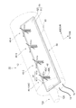
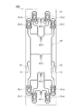
- FIG. 2 is a perspective view of the array antenna 30 according to the first embodiment.
- the array antenna 30 includes a plurality of (here, four as an example) cross-dipole antennas 40-1 to 40-4 (referred to as antenna 40 if not distinguished) and antennas 40-1 to 40-4. And a fixed substrate 50 as an example of a first substrate on which the distribution line 60 and the like are configured. Further, as shown in FIG. 3 to be described later, the array antenna 30 has phase shifters 70-1 to 70 for setting a phase difference (phase shift amount) of a transmission signal (received signal from the antenna 40) to the antenna 40. -6 (indicated as phase shifter 70 if not distinguished). Furthermore, the array antenna 30 includes a phase shift amount setting unit 120 that sets the phase shift amount of the phase shifter 70. It is assumed that the antennas 40-1 to 40-4 are arranged at equal intervals on the fixed substrate 50 at a predetermined distance.
- the antenna 40 includes a dipole antenna 41 that includes a radiating element portion 41a and a radiating element portion 41b that are formed of a conductor such as film-like copper or aluminum provided on a plate-like base member that is made of a dielectric.
- the dipole antenna 42 which is a combination of the radiating element portion 42a and the radiating element portion 42b, is combined.
- the radiating element portions 41a and 41b of the dipole antenna 41 are supplied with power from, for example, a power feeding portion formed of a conductor film on a base provided with the radiating element portions 41a and 41b.
- the dipole antenna 42 is the same as the dipole antenna 41. In FIG. 2, the base made of a dielectric is not shown.
- the base is, for example, a plate made of a dielectric such as a glass epoxy resin or a fluorine resin such as polytetrafluoroethylene. Note that it is preferable that the dielectric of the substrate has a small loss in the high frequency region.
- the radiating element portions 41a, 41b, 42a, 42b, and the power feeding portion may be configured of a conductive wire, a conductor plate, or the like without using the base.
- the antenna 40 and the dipole antennas 41 and 42 are examples of radiating elements.
- the dipole antenna 41 the direction connecting the radiating element portion 41a and the radiating element portion 41b is set to + 45 ° with respect to the vertical direction. Therefore, the dipole antenna 41 transmits + 45 ° polarization.
- the dipole antenna 42 the direction connecting the radiating element portion 42a and the radiating element portion 42b is set to ⁇ 45 ° with respect to the vertical direction. Therefore, the dipole antenna 42 transmits ⁇ 45 ° polarized wave. That is, the antenna 40 is a polarization sharing antenna.
- the direction connecting the radiating element portion 41a and the radiating element portion 41b of the dipole antenna 41 is set to the vertical direction, and the vertical polarization is set.
- a wave may be transmitted, and the direction connecting the radiating element part 42a and the radiating element part 42b of the dipole antenna 42 may be set in the horizontal direction to transmit the horizontally polarized wave.
- the antenna 40 is composed of a pair of dipole antennas 41 and 42, it may be a patch antenna or the like.
- the fixed substrate 50 includes a plate-like base 51 made of a dielectric, a reflective conductor 52 serving as a reflector provided on the surface of the base 51 on the antenna 40 side, and a surface of the base 51 opposite to the antenna 40. And a distribution line 60 provided (see FIG. 3 described later). Similarly to the distribution line 60, the fixed lines 71 and 72 of the phase shifter 70 are also provided on the surface of the base 51 opposite to the antenna 40 (see FIG. 4 described later). In addition, the base
- substrate 51 may be described with the board comprised with the dielectric material.
- the base 51 of the fixed substrate 50 is a plate made of a dielectric similar to the base of the antenna 40. Then, film-like conductors such as copper and aluminum are provided on both surfaces of the base 51.
- the conductor on the surface of the base 51 on the antenna 40 side is processed into a reflective conductor 52 that functions as a reflector, and the conductor on the surface opposite to the antenna 40 is a distribution line 60 and fixed lines 71 and 72 of the phase shifter 70.
- the fixed substrate 50 is provided with a through hole (see FIG. 4 described later) for fixing the antenna 40 and the phase shifter 70.
- the reflection conductor 52 reflects the radio wave and sets the directivity in the radio wave emission. Therefore, the reflective conductor 52 is in a state in which almost no conductor is left on the base 51 so as to have a uniform potential with respect to the antenna 40.
- the reflective conductor 52 is set to a reference potential such as a ground potential (GND).
- the reflective conductor 52 supplies a reference potential such as a ground potential (GND) to the distribution line 60 provided on the opposite side of the fixed substrate 50 from the antenna 40. That is, the reflective conductor 52 and the distribution line 60 constitute a microstrip line (line) transmission path. Therefore, the reflective conductor 52 may be referred to as a reference conductor. As will be described later, the reflective conductor 52 supplies a reference potential such as a ground potential (GND) to the fixed lines 71 and 72 and the movable line 82 of the phase shifter 70 (see FIGS. 4 and 7 described later). . That is, the reflective conductor 52, the fixed lines 71 and 72 of the phase shifter 70, and the movable line 82 constitute a microstrip line transmission path.
- GND ground potential
- the reflective conductor 52 is provided on the surface of the fixed substrate 50 on the antenna 40 side, and the distribution line 60, the fixed lines 71 and 72 of the phase shifter 70, and the movable line 82 are provided on the surface opposite to the antenna 40.
- a reflecting plate may be formed of an aluminum or copper plate and combined with the fixed substrate 50.
- the reflective conductor 52 of the fixed substrate 50 serves as a reference conductor that supplies a reference potential such as a ground potential (GND) to the distribution line 60, the fixed lines 71 and 72 of the phase shifter 70, and the movable line 82.
- the reflector may be connected to another potential or may be in a floating state. Any potential may be set as long as the characteristics to be obtained in the array antenna 30 are obtained.
- the phase shift amount setting unit 120 sets the phase shift amount of the plurality of phase shifters 70. In FIG. 2, only the knob 129 for setting the phase amount is shown. The phase shift amount setting unit 120 will be described later.
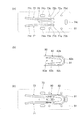
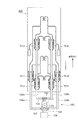
- FIG. 3 is a diagram for explaining the distribution circuit 200.
- FIG. 3A is a plan view of the distribution circuit 200
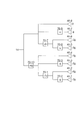
- FIG. 3B is a diagram for explaining the relationship between the signal transmitted to the antenna 40 and the phase shifter 70.
- the distribution circuit 200 is provided on the surface of the base 51 opposite to the antenna 40. Therefore, the plan view of the distribution circuit 200 shown in FIG. 3A is a view of the array antenna 30 shown in FIG. 2 as viewed from the back surface (below the paper surface of FIG. 2).
- FIG. 3B shows only a + 45 ° polarized signal.
- the distribution circuit 200 includes a plurality of transition lines connected by the distribution lines 60a to 60j and 60a 'to 60j' (indicated as the distribution line 60 when not distinguished).
- Phase shifter 70 phase shifters 70-1 to 70-6.
- the distribution circuit 200 includes end portions 61 and 62 connected to the transmission / reception cables 14 and 15, respectively. The end portions 61 and 62 may be connected to the transmission / reception cables 14 and 15 via a relay cable.
- the distribution circuit 200 distributes and supplies the signal generated by the transmission / reception unit in the base station to the antenna 40 (antennas 40-1 to 40-4), and combines the signals received from the radio waves by the antenna 40 to transmit / receive in the base station. To the department. At this time, the distribution circuit 200 sets the phase shift amount of the signal transmitted and received by the antenna 40 (antennas 40-1 to 40-4) by the plurality of phase shifters 70. Therefore, the distribution line 60 is a distribution / combination line that distributes / combines signals, and the distribution circuit 200 is a distribution / synthesis circuit that distributes / combines signals. Here, they are represented as a distribution line 60 and a distribution circuit 200.
- the fixed substrate 50 and the phase shifter 70 are an example of a distribution / synthesis device.
- the distribution circuit 200 may be referred to as a power feeding circuit.
- the power feeding unit includes a balun.
- the terminal 41d of the dipole antenna 41 and the terminal 42d of the dipole antenna 42 are connected to a reference potential such as a ground potential (GND).
- GND ground potential
- FIG. 3A only the antenna 40-1 is provided with a reference numeral. The same applies to the other antennas 40-2 to 40-4, but the reference numerals are omitted.
- the distribution circuit 200 is symmetrical on the left and right sides of FIG.
- an end 61 to which a transmission / reception cable 14 for transmitting a + 45 ° polarized signal is connected, distribution lines 60a to 60j, three phase shifters 70-1, 70-2, 70-3.
- an end 62 to which a transmission / reception cable 15 to which a signal of ⁇ 45 ° polarization is transmitted is connected, distribution lines 60a ′ to 60j ′, and three phase shifters 70-3 and 70 are provided.
- -4, 70-5 are provided.
- the lengths of the distribution lines 60a to 60j and 60a ′ to 60j ′ are set in consideration of signal delay.
- the left and right sides of the distribution circuit 200 are the same except that the polarization is different from + 45 ° and ⁇ 45 °. Therefore, the left side of the distribution circuit 200 will be described and the description on the right side will be omitted.
- a distribution line 60 extending from the end 61 to the terminal 41c of each power feeding unit of the antennas 40-1 to 40-4 will be described.
- the end 61 is connected to the distribution line 60a.
- the distribution line 60a branches into a distribution line 60b and a distribution line 60c.
- Distribution line 60b is connected to distribution line 60d via phase shifter 70-1.
- the distribution line 60d branches into a distribution line 60e and a distribution line 60f.
- Distribution line 60e is connected to distribution line 60g via phase shifter 70-2.
- Distribution line 60g is connected to terminal 41c of the feeding portion of dipole antenna 41 in antenna 40-1.
- the distribution line 60f is connected to the terminal 41c of the feeding portion of the dipole antenna 42 in the antenna 40-2.
- the distribution line 60c branches into a distribution line 60h and a distribution line 60i.
- Distribution line 60h is connected to distribution line 60j via phase shifter 70-3.
- the distribution line 60j is connected to the terminal 41c of the feeding part of the dipole antenna 41 in the antenna 40-3.
- the distribution line 60i is connected to the terminal 41c of the feeding part of the dipole antenna 41 in the antenna 40-4.
- a signal is transmitted to the antenna 40-1 (dipole antenna 41) via the phase shifter 70-1 and the phase shifter 70-2.
- a signal is transmitted to the antenna 40-2 (dipole antenna 41) via the phase shifter 70-1.
- a signal is transmitted to the antenna 40-3 (dipole antenna 41) via the phase shifter 70-3.
- a direct signal is transmitted to the antenna 40-4 (dipole antenna 41). Since the same applies to the dipole antenna 42, the description of the dipole antennas 41 and 42 in parentheses is omitted below.
- phase shift amount of the phase shifter 70-1 is -2 ⁇
- the phase shift amounts of the phase shifters 70-2 and 70-3 are - ⁇
- the phase amount is ⁇ 3 ⁇ for the antenna 40-1, ⁇ 2 ⁇ for the antenna 40-2, ⁇ for the antenna 40-3, and 0 for the antenna 40-4. That is, the phase shift amount becomes ⁇ between the adjacent antennas 40 (for example, between the antenna 40-1 and the antenna 40-2).
- the amount of phase shift of ⁇ increases the path length (line length) and causes a phase delay of the signal. Therefore, the radio wave emitted from the array antenna 30 is radiated at a tilt angle ⁇ determined by the distance between the antennas 40 and the phase shift amount ⁇ .
- phase shifters 70-2, 70-3, 70-5, and 70-6 set the phase shift amount to ⁇ and the phase shifter 70.
- the amount of phase shift may be set to -2.
- the phase shift amount setting unit 120 will be described later.
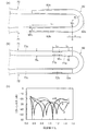
- FIG. 4 is a diagram for explaining the phase shifter 70.
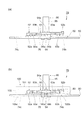
- 4A illustrates the fixed lines 71 and 72 provided on the fixed substrate 50 of the phase shifter 70
- FIG. 4B illustrates the movable line provided on the movable substrate 80 of the phase shifter 70
- FIG. 4C is a plan view of the phase shifter 70 in which the fixed lines 71 and 72 and the movable line 82 in FIG. 4A are combined.
- the fixed lines 71 and 72 provided on the base 51 are wires provided on the fixed substrate 50, and the distribution lines 60a to 60j and 60a in the distribution line 60 described above. It is formed at the same time as '-60j'. For this reason, the fixed lines 71 and 72 may be considered as a part of the distribution line 60. In addition, it demonstrates as another thing here.
- the fixed line 71 includes a front end portion 71a, an intermediate portion 71b, and a rear end portion 71c. That is, the rear end portion 71 c is formed with a uniform width so as to have a predetermined characteristic impedance Z 0 with respect to the reflective conductor 52. Moreover, the front-end
- a part of the end portion 72 c is configured in parallel on the base 51.
- the phase shifter 70 is the phase shifter 70-1
- the rear end portion 71c of the fixed line 71 is connected to the distribution line 60b
- the rear end portion 72c of the fixed line 72 is connected to the distribution line 60d.
- the movable substrate 80 as an example of the second substrate includes a plate-like base body 81 made of a dielectric and a movable line 82 provided on the base body 81.
- the base 81 may be described as a plate made of a dielectric.
- the movable line 82 includes, for example, a central portion 82a bent in a U-shape, and end portions 82b and 82c that gradually become narrower from the central portion 82a.
- the central portion 82a is a portion that connects the end portions 82b and 82c.
- the center part 82a was made into U shape, another shape may be sufficient.
- the central portion 82 a is configured wider than the rear end portion 71 c of the fixed line 71 and the rear end portion 72 c of the fixed line 72.
- the shapes of the fixed lines 71 and 72 and the movable line 82 will be described later.
- the phase shifter 70 turns the movable substrate 80 over so that the movable line 82 of the movable substrate 80 faces the fixed lines 71 and 72 on the base 51. It is arranged on the fixed substrate 50. And the front-end
- a dielectric film 83 (see FIG.
- the holding member 90 and the covering member 100 can maintain a constant distance in a state where the movable line 82 is pressed in the direction of the fixed lines 71 and 72, and the VSWR characteristic and the phase shift can be maintained. The characteristics can be stabilized.
- the signal is input from the rear end portion 71c of the fixed line 71 and propagates to the intermediate portion 71b and the front end portion 71a. Then, the signal is electrically coupled via the dielectric film 83 from the rear end portion 71c, the intermediate portion 71b, and the front end portion 71a of the fixed line 71 that overlaps the end portion 82b of the movable line 82, and the movable line 82 Propagate to the end 82b of the. The signal propagates through the central portion 82a of the movable line 82.
- the fixed line 71 is an example of a first line conductor
- the fixed line 72 is an example of a second line conductor
- the movable line 82 is an example of a third line conductor.
- the movable line 82 is moved along the longitudinal direction of the fixed lines 71 and 72.
- the U-shaped movable line 82 is provided so as to short-circuit the two fixed lines 71 and 72. Therefore, moving the movable line 82 on the two fixed lines 71 and 72 causes a difference in the path length through which the signal propagates.
- Such a phase shifter 70 may be called a trombone type phase shifter.
- the movable line 82 is moved in the longitudinal direction of the fixed lines 71 and 72 here, the movable line 82 may be fixed and the fixed lines 71 and 72 may be moved. That is, the movement of the movable line 82 relative to the fixed lines 71 and 72 is relative.
- the fixed substrate 50 has through holes 73a, 73b, 73c, 73d provided through the fixed substrate 50 in order to fix the presser member 90 and the cover member 100 described later.
- 74a, 74b, 74c, 76 are provided.
- the covering member 100 may be referred to as a housing or a case.
- the through holes 73a, 73b, 73c, 73d have a circular planar shape.
- the movable substrate 80 is provided outside the movable substrate 80 on the long side so as to surround the movable substrate 80.
- the through holes 74 a, 74 b and 74 c are provided to fix the covering member 100 to the fixed substrate 50.
- the through holes 74 a, 74 b, and 74 c have a rectangular shape, and a return (claw-like protrusion) provided at the tip of the convex portions 105 a, 105 b, and 105 c of the covering member 100 is a fixed substrate 50, as will be described later. It is provided so as to protrude to one surface side (the reflective conductor 52 side) and be caught by the fixed substrate 50.
- the through hole 76 is a long hole that guides the movement of the convex portions 96a and 96b of the pressing member 90 provided to move the movable substrate 80 (see FIG. 12 described later).
- the movable substrate 80 is provided with through holes 83 a and 83 b provided through the movable substrate 80.
- columnar convex portions 96a and 96b provided in the pressing member 90 are inserted into the through holes 83a and 83b.
- the convex portions 96 a and 96 b protruding from the through holes 83 a and 83 b are inserted into the through holes 76 provided in the fixed substrate 50.
- the through holes 73 a, 73 b, 73 c, 73 d, 74 a, 74 b, 74 c, 76 provided through the fixed substrate 50 will be described together with the pressing member 90 and the covering member 100.
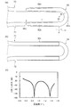
- FIG. 5 is an enlarged view of the fixed lines 71 and 72 provided on the fixed substrate 50 of the phase shifter 70 shown in FIG. 4 and the movable line 82 provided on the movable substrate 80.
- 5A shows the movable line 82
- FIG. 5B shows the fixed lines 71 and 72
- FIG. 5C shows the return loss characteristic of the phase shifter 70.
- FIG. 5C shows the return loss characteristic with respect to the movement amount x between the fixed lines 71 and 72 and the movable line 82.
- the horizontal axis represents the frequency f / f 0 with respect to the center frequency f 0
- the vertical axis represents the return loss (dB).
- the central portion 82a of the movable line 82 has a width W C is 2.1 mm, the radius of curvature R is 3.8 mm.
- End 82b of the movable line 82, 82c has a width W TE of the gradually thinner becomes the tip from the width Wc of the center portion 82a (2.1 mm) is 1.1 mm.
- the end portions 82b, 82c has a length L T is 18.1 mm.
- the fixed line 71 has a length L t is 1.1mm tip portion 71a, the width W e is 1.7 mm, the length L m of the intermediate portion 71b is 2.9 mm, a width W m is 1.1 mm, and the width W t of the rear end 71c is 1.7 mm.
- the fixed line 72 has a length L t is 1.1mm tip portion 71a, the width W e is 1.7 mm, the length L m of the intermediate portion 71b is 2.9 mm, a width W m is 1.1 mm, and the width W t of the rear end 71c is 1.7 mm.
- the fixed line 72 has a length L t is 1.1mm tip portion 71a, the width W e is 1.7 mm, the length L m of the intermediate portion 71b is 2.9 mm, a width W m is 1.1 mm, and the width W t of the rear end 71c is 1.7 mm.
- the fixed line 72
- FIG. 5C shows the state of FIGS. 5A and 5B in which the movement amount x is 0 mm, and the movement line x is moved to the right in FIG. 5A. It shows the return loss characteristic when is assumed to be positive. As shown in FIG. 5C, the return loss is around ⁇ 20 dB at any position where the movement amount x is ⁇ 2 mm to 6 mm, which is smaller than the case shown in FIG. For example, the standing wave ratio VSWR is 1.2 or less (return loss ⁇ 20.8 dB or less), the specific bandwidth is wide, and the bandwidth is wide (widened).
- FIG. 6 is an enlarged view of the fixed lines 71 and 72 provided on the fixed substrate 50 and the movable line 82 provided on the movable substrate 80 of the phase shifter 70 to which the first embodiment is not applied.
- 6A shows the movable line 82
- FIG. 6B shows the fixed lines 71 and 72
- FIG. 6C shows the return loss characteristic of the phase shifter 70.
- the return loss characteristic is shown in relation to the amount of movement x between the fixed lines 71 and 72 and the movable line 82, as in FIG. 5C.
- the horizontal axis represents the frequency f / f 0 with respect to the center frequency f 0
- the vertical axis represents the return loss (dB).
- the movable line 82 includes a central portion 82a and end portions 82b, the width W M of 82c is 1.8 mm.
- the movable track 82 has a radius of curvature R of the central portion 82a of 3.75 mm.
- the fixed line 71 is 1.8mm width W s. That is, the fixed line 71 does not have the front end portion 71a, the intermediate portion 71b, and the rear end portion 71c of the fixed line 71 of the phase shifter 70 to which the first embodiment shown in FIG. 5 is applied.
- FIG. 7 is a diagram for explaining the characteristics of the phase shifter 70 to which the first embodiment shown in FIG. 5 is applied.
- 7A is a plan view as viewed from the movable line 82 side
- FIG. 7B is a plan view as viewed from the fixed lines 71 and 72 side
- FIG. 7C is a plan view as illustrated in FIGS. It is sectional drawing in the VIIC-VIIC line of b).
- 7A is FIG. 5A
- FIG. 7B is FIG. 5B.
- FIG. 7C shows a fixed line 71 (front end portion 71a, intermediate portion 71b, rear end portion 71c) and movable line 82 (center portion 82a, end portion 82b).
- the fixed line 71 (the same applies to the fixed line 72, the same part is represented by () below) and the movable line 82 with respect to the reflective conductor 52 provided on the antenna 40 side of the fixed substrate 50, A microstrip line is formed.
- the characteristic impedance of the fixed line 71 (fixed line 72) is determined by the width of the fixed line 71 (fixed line 72), the dielectric constant ⁇ M of the base 51, and the thickness d1.
- the movable line 82 is located on the fixed lines 71 and 72.
- a dielectric film 83 is often provided between the fixed lines 71 and 72 and the movable line 82.
- the movable line 82 is, for example, a portion that does not overlap with the fixed line 71 (fixed line 72) like the central part 82a shown in FIG. Is greater than the fixed lines 71 and 72.
- the characteristic impedance of such a portion of the movable line 82 includes the width of the movable line 82, the dielectric constant ⁇ M and the thickness d1 of the base 51, and the dielectric constant ⁇ A and the thickness (d2-d1) of the intervening air layer. Determined by.
- the fixed line 71, the movable line 82 the difference in impedance is suppressed.
- the characteristic impedance of the microstrip line is such that the lines (fixed lines 71 and 72 and the movable line 82), which are signal propagation paths, and the reference conductor (here, the reflective conductor 52) when the line width is constant. ), The larger the distance, the smaller the line (the fixed lines 71 and 72 and the movable line 82) through which the signal propagates.
- the distance d2 from the central portion 82a is reflected conductor 52 of the movable track 82 is greater than the distance d1 of the fixed line 71 and 72, the width W C of the central portion 82a, the rear end portion 71c of the fixed line 71 and 72, It is set to be larger than the width W e of 72c.
- the widths of the end portions 82b and 82c decrease as the distance from the central portion 82a increases. Therefore, when the movable line 82 is moved to the right side of FIG. 7A (the direction in which the movement amount x is positive), the characteristic impedance increases at the part where the signal propagates from the fixed lines 71 and 72 to the movable line 82.
- the fixed line 71 and 72, intermediate portions 71b, 72b a width W m of the rear end portion 71c of, and smaller than the width W e of 72c. Therefore, the intermediate portions 71b and 72b have a high impedance.
- the end portions 82b and 82c of the movable line 82 protrude from the intermediate portions 71b and 72b. For this reason, the impedance of the overlapping portion is in parallel with the impedance of the intermediate portions 71b and 72b and the impedance of the protruding portion of the end portions 82b and 82c of the movable line 82.
- the fixed lines 71 and 72 on the fixed substrate 50 and the movable line 82 on the movable substrate 80 are connected to the fixed lines 71 and 72.
- the return loss is suppressed as a shape in which a large change in impedance is unlikely to occur in the signal propagation path.
- FIG. 8 shows another example of the shapes of the fixed lines 71 and 72 and the movable line 82 in the phase shifter 70.
- 8A is a plan view as viewed from the movable line 82 side
- FIG. 8B is a plan view as viewed from the fixed lines 71 and 72
- FIG. 8C is a return loss of the phase shifter 70. It is a figure which shows a characteristic.
- the movable line 82 has a central portion 82a, and the end portions 82b and 82c are narrowed in two steps from the central portion 82a.
- Central portion 82a of the movable line 82 has a width W C is 2.1 mm, the radius of curvature R is 3.8 mm.
- the end portion 82b of the movable line 82 has a length W T1 of 1.7 mm and a length L on the opposite side of the central portion 82a in the length L T1 (10 mm) of the length L T (19 mm) on the central portion 82a side.
- the width W T2 is 1.3 mm at T2 (7 mm).
- the end portion 82c of the movable line 82 has the same shape as the end portion 82b.
- the intermediate portions 71b and 72b are narrowed, and the tip portions 71a and 72a are provided with cuts.
- the width W t of the front end portion 71a and the width W e of the rear end portion 71c are 1.9 mm.
- Intermediate portion 71b has a width W m is 1.1 mm, a length L m is 3.1 mm.
- the front end 71 a is cut in the longitudinal direction of the fixed line 71.
- the length L t2 of the portion length L t1 of a portion facing the inside of the central portion 82a is opposed 4.6 mm, the outside of the movable line 82 is 5 mm.
- the return loss when the movement amount x is 0 mm is around ⁇ 20 dB, and the standing wave ratio VSWR is at a frequency of 0.59 f / f 0 or more. Is 1.2 or less and the specific bandwidth is wide (broadband).
- FIG. 9 shows still another example of the shapes of the fixed lines 71 and 72 and the movable line 82 in the phase shifter 70.
- 9A is a plan view as viewed from the movable line 82 side
- FIG. 9B is a plan view as viewed from the fixed lines 71 and 72
- FIG. 9C is a return loss of the phase shifter 70. It is a figure which shows a characteristic.
- the movable line 82 is the same as the movable line 82 shown in FIG. 5, and the widths of the end portions 82b and 82c are gradually narrowed from the central portion 82a.
- Central portion 82a of the movable line 82 has a width W C is 2.1 mm, the radius of curvature R is 3.8 mm. End 82b of the movable line 82, the width W TE of the gradually thinner becomes the tip from the width Wc of the center portion 82a (2.1 mm) is 1.1 mm. The length L T of the end portion 82b is 19 mm.
- the fixed lines 71 and 72 are the same as the fixed lines 71 and 72 shown in FIG. 6 and have the same width.
- Fixed line 71, the width W s is 1.7 mm.
- the return loss when the movement amount x is 0 mm is around ⁇ 20 dB, and the standing wave ratio VSWR is at a frequency of 0.68 f / f 0 or more. Is 1.2 or less and the specific bandwidth is wide (broadband).
- FIG. 10 shows still another example of the shapes of the fixed lines 71 and 72 and the movable line 82 in the phase shifter 70.
- 10A is a plan view as viewed from the movable line 82 side
- FIG. 10B is a plan view as viewed from the fixed lines 71 and 72
- FIG. 10C is a return loss of the phase shifter 70. It is a figure which shows a characteristic.
- the movable line 82 has a central portion 82a similar to the movable line 82 shown in FIG. 8 (a), and the end portions 82b and 82c are in two stages from the central portion 82a. It is getting thinner.
- Central portion 82a of the movable line 82 has a width W C is 2.1 mm, the radius of curvature R is 3.8 mm.
- the width W T2 is 1.3 mm at T2 (7 mm).
- the end portion 82c of the movable line 82 has the same shape as the end portion 82b.
- the fixed lines 71 and 72 are the same as the fixed lines 71 and 72 shown in FIG. 6 and have the same width.
- Fixed line 71, the width W s is 1.7 mm.
- the return loss when the movement amount x is 0 mm is around ⁇ 20 dB, and the standing wave ratio VSWR is at a frequency of 0.66 f / f 0 or more. Is 1.2 or less and the specific bandwidth is wide (broadband).
- the fixed lines 71 and 72 and the movable line 82 of the phase shifter 70 have a shape in which a large change in impedance is unlikely to occur in the signal propagation path, that is, the impedance fluctuation in the signal propagation path. Any shape that can be suppressed may be used. Therefore, shapes other than those described above may be used. For example, the widths of the fixed lines 71 and 72 overlapping the movable line 82 or the whole or a part of the movable line 82 may be narrowed or thickened.
- a rotary type phase shifter that sets a phase shift amount by intersecting a plurality of arc-shaped conductors (arc-shaped conductors) and a linear conductor (linear conductor) has been used.
- the rotary type phase shifter can set a plurality of phase shift amounts at a time, but the diameter of the arcuate conductor increases as the number of required phase shift amounts increases. For this reason, when the phase shifter is provided on the back side of the array antenna 30, the width in the horizontal direction becomes large, and it is difficult to reduce the diameter of the sector antenna 10.
- a plurality of phase shifters 70 are distributed and used in the distribution circuit 200, but each phase shifter 70 is small as described above. Therefore, the sector antenna 10 can be easily reduced in diameter as compared with a rotary phase shifter using an arcuate conductor.
- phase shifter 70 the position of the movable line 82 is set with respect to the fixed lines 71 and 72 so as to correspond to the required tilt angle ⁇ .
- the phase shifter 70 moves (slides) the movable line 82 with respect to the fixed lines 71 and 72. Thereby, the position where the fixed lines 71 and 72 and the movable line 82 overlap is moved (slid). Then, a phase shift amount corresponding to the tilt angle ⁇ is set. That is, the movable track 82 needs to be easily moved (slid) with respect to the fixed tracks 71 and 72 and held at the moved position. Next, the holding mechanism in the phase shifter 70 will be described.
- FIG. 11 is a diagram illustrating a holding mechanism that holds the movable substrate 80 in the phase shifter 70.
- FIG. 11A is a perspective view of the phase shifter 70 provided with a holding mechanism
- FIG. 11B is a top view of the phase shifter 70 viewed from the XI direction of FIG. 11A.
- the holding mechanism includes a pressing member 90 and a covering member 100.
- the covering member 100 is indicated by a broken line.
- the fixed lines 71 and 72 of the phase shifter 70 are provided on the fixed substrate 50 together with the distribution line 60.
- the movable line 82 of the phase shifter 70 is provided on the movable substrate 80.
- the side of the fixed substrate 50 on which the fixed lines 71 and 72 are provided and the side of the movable substrate 80 on which the movable line 82 is provided are arranged so as to face each other.
- the dielectric film 83 is sandwiched between the fixed substrate 50 and the movable substrate 80 in order to maintain a certain distance from the fixed substrate 50.
- the dielectric film 83 is attached to the movable line 80 side of the movable substrate 80.
- the fixed lines 71 and 72 and the movable line 82 are the same as those shown in FIGS. 5 (a) and 5 (b).
- the central portion 82a of the movable line 82 is the left front side in FIG. 11A, the left side in FIG. 11B, the end portions 82b and 82c are the right back side in FIG. 11A, and FIG. In the right side.
- the holding member 90 includes three spring portions 91, 92, 93 whose longitudinal direction extends in the sliding (sliding) direction so as to press the movable substrate 80 against the fixed substrate 50.
- the three spring portions 91, 92, 93 are provided in parallel with the moving (sliding) direction of the movable substrate 80. And it is mutually connected by the connection part 94 which connects each center part mutually.
- a columnar convex portion 95 is provided on the connecting portion 94 so as to protrude in a direction away from the movable substrate 80.
- one of the three spring portions 91, 92, 93 provided in parallel with the other spring portion 91 located on the outer side includes protrusions 91a, 91b on the movable substrate 80 side of the tip portion ( (It is not shown because it is behind the spring portion 91).
- the protrusions 91a and 91b are in contact with (pressed against) the movable substrate 80.
- the other spring part 93 located on the outer side includes protrusions 93a and 93b on the movable substrate 80 side of the tip part (see FIG. 12).
- the protrusions 93a and 93b are in contact with (pressed against) the movable substrate 80.
- the spring portion 92 located at the center includes a protrusion 92 a on the movable substrate 80 side on one tip side of the movable substrate 80 (on the central portion 82 a side of the movable line 82).
- the protrusion 92a is in contact (pressing) with the movable substrate 80.
- a protrusion 92 b is provided on the opposite side of the movable substrate 80 on the other tip side of the movable substrate 80 (ends 82 b and 82 c side of the movable line 82).
- the connecting portions 94 on the spring portions 91 and 93 are provided with protrusions 94a and 94b on the opposite side to the movable substrate 80, respectively.
- the spring portions 91 and 93 located on the outer side protrude to the covering member 100 side so that the respective tip portions thereof are in contact with the covering member 100 described below. By doing so, the presser member 90 is accommodated in the cover member 100 without rattling.
- the pressing member 90 includes two columnar convex portions 96a and 96b that protrude to the movable substrate 80 side (see FIGS. 12A and 12B). This is inserted into the through holes 83a and 83b of the movable substrate 80 shown in FIG. 4 (b), and the tip thereof is a long hole provided in the fixed substrate 50 shown in FIG. 4 (a). It is inserted into a certain through hole 76.
- the covering member 100 covers the movable substrate 80 and the pressing member 90 and fixes the pressing member 90.
- the covering member 100 includes a lid portion 101 and a side surface portion 102 that surrounds the periphery of the lid portion 101.
- the covering member 100 includes four columnar convex portions 103a, 103b, 103c, and 103d that protrude from the side surface portion 102 to the side opposite to the lid portion 101 side. These convex portions 103a, 103b, 103c, and 103d have a circular cross section. Two are provided on both outer sides in the moving direction x of the movable substrate 80. The cross section need not be a circle.
- the covering member 100 includes three convex portions 105a, 105b, and 105c that protrude from the side surface portion 102 to the side opposite to the lid portion 101 side.
- the convex portions 105 a, 105 b, and 105 c have tips that are bent back and are bent outwardly from the covering member 100 into an L shape. Further, the covering member 100 includes an opening 106 in the lid portion 101.
- the convex portions 103a, 103b, 103c, and 103d are inserted into through holes 73a, 73b, 73c, and 73d provided in the fixed substrate 50.
- the through holes 73a, 73b, 73c, and 73d can be formed into circles having a precise planar shape by a drill or the like. Therefore, the cover member 100 is arranged with high positional accuracy with respect to the fixed substrate 50 by making the cross-sectional shape of the convex portions 103a, 103b, 103c, and 103d into a circle.
- the convex portions 105 a, 105 b, and 105 c are inserted into through holes 74 a, 74 b, and 74 c provided in the fixed substrate 50. Then, the cover member 100 is fixed to the fixed substrate 50 by the return of the tip bent in an L shape turning around to the reflective conductor 52 side of the fixed substrate 50.
- the movable substrate 80 moves (slides) on the fixed substrate 50 by moving the convex portion 95 within the opening 106 provided in the lid portion 101.
- a scale may be provided on the lid 101 in the vicinity of the opening 106 in order to set the amount of movement of the movable substrate 80.
- FIG. 12 is a cross-sectional view illustrating a holding mechanism that holds the movable substrate 80 in the phase shifter 70.
- 12A is a view showing a state in which the movable substrate 80 and the pressing member 90 are arranged on the fixed substrate 50
- FIG. 12B is a diagram in which the fixing substrate 50 and the pressing member 90 are further fixed by the covering member 100. It is a figure which shows a state.
- 12A and 12B are cross-sectional views taken along line XII-XII in FIG. 11B.
- the dielectric film 83 is not shown.
- the movable substrate 80 and the pressing member 90 are disposed on the fixed substrate 50.
- a convex portion 96 a provided so as to protrude toward the movable substrate 80 of the pressing member 90 is inserted into the through hole 83 b of the movable substrate 80.
- the convex portion 96 b is inserted into the through hole 83 a of the movable substrate 80.
- the tip portions protruding from the movable substrate 80 of the convex portions 96 a and 96 b are inserted into the through holes 76 which are long holes provided in the fixed substrate 50.
- the through holes 83a and 83b are accurately formed by a round tool such as a drill (end mill). Therefore, by making the convex portions 96a and 96b of the pressing member 90 cylindrical, the movable substrate 80 is restrained by the convex portions 96a and 96b of the pressing member 90 inserted into the through holes 83a and 83b. Further, the convex portions 96 a and 96 b are restricted so as to move in the through hole 76 which is a long hole provided in the fixed substrate 50.
- the relative position between the movable line 82 of the movable substrate 80 and the fixed lines 71 and 72 provided on the fixed substrate 50 is set with high accuracy, and the movable line 82 is predetermined with respect to the fixed lines 71 and 72. Out of the range of the movement amount x is suppressed.
- the two through holes 83a and 83b and the two convex portions 96a and 96b it is possible to suppress tilting in a direction intersecting the movement (sliding) direction (direction of the movement amount x). .
- a covering member 100 is provided.
- the convex portions 105 a, 105 b, and 105 c of the covering member 100 are fitted into the through holes 74 a, 74 b, and 74 c provided in the fixed substrate 50.
- the inside of the lid portion 101 of the covering member 100 hits the protrusion 94 a (protrusion 94 b) of the connecting portion 94 of the pressing member 90.
- the cover part 101 of the cover member 100 presses the connection part 94 of the pressing member 90 to the movable substrate 80 side on the inner side.
- the spring portions 91 and 93 on both outer sides of the pressing member 90 are formed in an arch shape that is recessed toward the movable substrate 80 when the connecting portion 94 is pressed. Therefore, the protrusions 91 a and 91 b provided at both ends of the spring portion 91 and the protrusions 93 a and 93 b provided at both ends of the spring portion 93 press the movable substrate 80 toward the fixed substrate 50. Similarly, the protrusion 92 a provided at one end of the spring portion 92 of the pressing member 90 presses the movable substrate 80 toward the fixed substrate 50, and the protrusion 92 b provided at the other end is the lid portion 101 of the covering member 100. It is pressed inside.
- the protrusion 92 b provided at the other end serves as a fulcrum, and the protrusion 92 a provided at the one end is pressed more strongly against the movable substrate 80. That is, the pressing member 90 has a spring function (spring mechanism) by being pressed by the lid portion 101 of the covering member 100.
- the movable substrate 80 has the projections 91a, 91b, 92a, 93a, 93b of the spring portions 91, 92, 93 of the pressing member 90 in the regions ⁇ , ⁇ , ⁇ , ⁇ shown in FIG. It is strongly pressed against the fixed substrate 50.
- the regions ⁇ , ⁇ , ⁇ , ⁇ , and ⁇ correspond to the movable line 82 of the movable substrate 80 as shown in FIG. That is, the holding member 90 is provided with protrusions 91a, 91b, 92a, 93a, 93b so that the movable line 82 can be pressed to the fixed substrate 50 side.
- the holding member 90 and the covering member 100 are made of polycarbonate, for example.
- the pressing member 90 and the covering member 100 are comprised with the same material. By constituting with the same material, it is suppressed that a mutual position shifts by thermal expansion.
- ⁇ Phase shift amount setting unit 120> In the distribution circuit 200 described with reference to FIG. 3B, the six phase shifters 70 are set to the phase shift amount ⁇ and the phase shift amount 2 ⁇ . That is, the phase shift amounts of the plurality of phase shifters 70 are set to different values in a proportional relationship.
- FIG. 13 is a diagram illustrating the phase shift amount setting unit 120.
- the phase shift amount setting unit 120 includes a screw part 121 having a pitch p1 and a screw part 123 having a pitch p2 that are linearly configured on one axis.
- a nut 122 is fitted into the screw part 121, and a nut 124 is fitted into the screw part 123.
- the screw part 121 and the screw part 123 rotate simultaneously by rotating the shaft.
- the pitch p2 is twice the pitch p1.
- the screw rotation directions of the screw portions 121 and 123 (the direction in which the nuts 122 and 124 advance) are the same.
- the screw parts 121 and 123 may be any member having a male screw.
- the screw part 121 is an example of a first male screw part
- the screw part 123 is an example of a second male screw part
- the nuts 122 and 124 may be any member having a female screw
- the nut 122 is an example of a first female screw part
- the nut 124 is an example of a second female screw part.
- the pitch p1 is an example of the first pitch
- the pitch p2 is an example of the second pitch.
- the phase shift amount setting unit 120 includes an attachment member 125 attached to the nut 122 and connection members 126a and 126b attached to the attachment member 125. Furthermore, the phase shift amount setting unit 120 includes an attachment member 127 attached to the nut 124 and connection members 128a and 128b attached to the attachment member 127.
- the connection member 126a is connected to the respective support columns 95 (see FIG. 11A) of the phase shifters 70-2 and 70-3.
- the connection member 126b is coupled to the respective support columns 95 of the phase shifters 70-5 and 70-6.
- the connecting member 128a is connected to the support column 95 of the phase shifter 70-1.
- the connecting member 128b is connected to the support column 95 of the phase shifter 70-4.
- the phase shift amount setting unit 120 includes a rotary knob 129 connected to a common shaft of the screw part 121 and the screw part 123.
- the nut 122, the attachment member 125, and the connection members 126a and 126b are examples of a first moving member
- the nut 124, the attachment member 127, and the connection members 128a and 128b are examples of a second movement member.
- the knob 129 By turning the knob 129, the screw portions 121 and 123 rotate, and the nuts 122 and 124 move. Accordingly, the mounting members 125 and 127 connected to the nuts 122 and 124 move in the x direction. Then, the connection members 126a, 126b, 128a, and 128b connected to the attachment members 125 and 127 move in the x direction. As the connecting members 126a, 126b, 128a, and 128b move, the movable substrate 80 of the phase shifter 70 of the connected support column 95 moves relative to the fixed substrate 50. That is, the rotation of the knob 129 is converted into a linear motion of the connection members 126a, 126b, 128a, and 128b. Further, the rotation of the knob 129 is converted into the movement of the movable substrate 80 of the phase shifter 70 relative to the fixed substrate 50 by the support column 95 coupled to the connecting members 126a, 126b, 128a, and 128b.
- the nut 122 is assumed to move a distance a in the x direction (the direction of the movement amount x of the phase shifter 70). Then, in the threaded portion 123, the nut 124 moves a distance 2a in the x direction. Then, the connection members 126a and 126b attached to the nut 122 with the attachment member 125 move a in the x direction. Further, the connection members 128a and 128b attached to the nut 124 with the attachment member 127 move 2a in the x direction. If the movement of a in the x direction corresponds to the phase shift amount ⁇ , the phase shifters 70-2, 70-3, 70-5, and 70-6 are set to the phase shift amount ⁇ .
- the devices 70-1 and 70-4 are set to the phase shift amount 2 ⁇ . That is, even if the phase shifters 70-1 and 70-4 and the phase shifters 70-2, 70-3, 70-5, and 70-6 have the same configuration, different phase shift amounts are set simultaneously.
- the phase shift amount ⁇ is an example of the first phase shift amount
- the phase shift amount 2 ⁇ is an example of the second phase shift amount.
- FIG. 14 is an enlarged view of the screw parts 121 and 123.
- the phase shift amount setting unit 120 includes a support member 130 (not shown in FIG. 13).
- the phase shift amount setting unit 120 is fixed to the lower lid of the radome 12 shown in FIG.
- the pitch p ⁇ b> 2 of the screw part 123 is twice the pitch p ⁇ b> 1 of the screw part 121.
- the diameter of the thread part 123 of pitch p2 (> pitch p1) is larger than the diameter of the thread part 121 of pitch p1. In general, this is because a screw having a large amount to be fed, that is, a screw having a large pitch, has a large diameter, and the diameters of the screw portions 121 and 123 may be the same or reversed.
- the nut 122 of the screw part 121 is composed of sub-nuts 122a and 122b each corresponding to a half-pitch thread.
- the sub-nuts 122a and 122b are fixed with screws or the like so as to overlap and sandwich one screw thread. Thereby, even if the nut 122 is moved in the screw part 121, occurrence of backlash (backlash) is suppressed.
- the nut 124 of the threaded portion 123 is composed of sub-nuts 124a and 124b each corresponding to a half pitch thread.
- the pitch p2 of the screw portion 123 is set so that the movement amount x in the phase shifters 70-1 and 70-4 having a large movement amount x is maximized by one rotation of the rotary knob 129. Therefore, a 360 ° scale is provided around the rotary knob 129.
- the amount of movement x, that is, the phase shift amount ⁇ is set by rotating the rotary knob 129 with this scale as a guide.
- a motor may be connected to the knob 129, or a motor may be used instead of the knob 129.
- the movement amount x, that is, the phase shift amount ⁇ is set by monitoring the rotation angle of the motor. In this case, it is not necessary to provide a scale around the rotary knob 129.
- a ruler may be provided on the connecting members 126a, 126b, 128a, and 128b, and the movement amount x with respect to the reference point may be read using the ruler.
- the maximum movement amount x is as small as 3.5 mm, for example, it is not easy to read the movement amount x from the ruler. Therefore, the movement amount x (phase shift amount ⁇ ) is accurately set by a 360 ° scale provided around the knob 129.
- phase shift amount ⁇ and phase shift amount 2 ⁇ are set, but the phase shift amount is set to the same (phase shift amount ⁇ ). Also good.
- phase shift amount setting unit 120 is configured by a thread portion having one pitch. That is, it is not necessary to provide the screw part 123.
- the phase shift amount setting unit 120 is configured by screw portions 121 and 123 having different pitches provided on one axis.
- a rack and pinion or a worm gear may be used.
- racks having the same pitch are provided in the moving directions of the attachment members 125 and 127, gears (pinions) having different numbers of teeth are connected, and the pinion is rotated.
- the racks provided on the attachment members 125 and 127 are provided in the vertical direction in FIG. For this reason, the pinion combined with the rack easily moves downward in the vertical direction due to gravity.
- phase shift amount setting unit 120 when the phase shift amount setting unit 120 is configured by the screw portions 121 and 123, the accuracy of setting the phase shift amount ⁇ is higher than when the rack and pinion is used. Further, since the nut 122 is composed of two sub-nuts 122a and 122b and the nut 124 is composed of two sub-nuts 124a and 124b, it is difficult to move downward in the vertical direction and backlash. A decrease in accuracy due to the above is suppressed.
- the phase shift amount setting unit 120 moves a plurality of connection members (for example, the connection members 126a and 126b and the connection members 128a and 128b) at a predetermined ratio so that a plurality of phase shift amounts can be set. Anything that can do.
- FIG. 15 is a diagram illustrating the distribution circuit 200 according to the second embodiment.
- the array antenna 30 includes eight antennas 40 (antennas 40-1 to 40-8). It is assumed that the antennas 40-1 to 40-8 are arranged at equal intervals at a predetermined distance from the lower side to the upper side in the vertical direction.
- the array antenna 30 has a configuration in which two array antennas 30 of the first embodiment are arranged in the vertical direction. On the lower side in the vertical direction, array antenna 30 of the first embodiment including antennas 40-1 to 40-4 (hereinafter referred to as array antenna 30-1) is provided.
- an array antenna 30-2 similar to the array antenna 30 of the first embodiment including antennas 40-5 to 40-8 and phase shifters 70-7 to 70-12 is provided. It has been. On the outside thereof, phase shifters 70-13 and 7-14 are provided.
- the transmission / reception cable 14 is connected to the end 61, and the distribution line 60 from the end 61 is branched into two.
- One of the branched distribution lines 60 is connected to the lower array antenna 30-1 via the phase shifter 70-13.
- the other of the branched distribution lines 60 is connected to the upper array antenna 30-2.
- each distribution line 60 is not labeled.
- the transmission / reception cable 15 is connected to the end portion 62, and the distribution line 60 is branched into two from the end portion 62.
- One of the branched distribution lines 60 is connected to the lower array antenna 30-1 via the phase shifter 70-14.
- the other of the branched distribution lines 60 is connected to the upper array antenna 30-2.
- left and right are symmetrical, the left side corresponds to + 45 ° polarization, and the right side corresponds to ⁇ 45 ° polarization.
- FIG. 16 is a diagram for explaining the amount of phase shift in the array antenna 30 shown in the second embodiment.
- FIG. 16 shows the left side corresponding to + 45 ° polarization in FIG.
- the phase shifters 70-1 and 70-7 are set to the phase shift amount -2 ⁇
- the phase shifters 70-2, 70-3, 70-8 and 70-9 are set to the phase shift amount - ⁇ .
- the phase shifter 70-13 is set to the phase shift amount ⁇ 4 ⁇ .
- the antenna 40-8 has a phase shift amount of 0,
- the antenna 40-7 has a phase shift amount of ⁇
- the antenna 40-6 has a phase shift amount of ⁇ 2 ⁇
- the antenna 40-5 has a phase shift amount of ⁇ 3 ⁇
- the antenna 40-4 is a diagram for explaining the amount of phase shift in the array antenna 30 shown in the second embodiment.
- FIG. 16 shows the left side corresponding to + 45 ° polarization in FIG.
- the phase shifters 70-1 and 70-7 are set to the phase shift amount -2 ⁇
- the antenna 40-3 is set to the phase shift amount ⁇ 5 ⁇
- the antenna 40-2 is set to the phase shift amount ⁇ 6 ⁇
- the antenna 40-1 is set to the phase shift amount ⁇ 7 ⁇ . That is, the amount of phase shift is ⁇ between adjacent antennas 40 (for example, antenna 40-1 and antenna 40-2). Therefore, the array antenna 30 is set to a tilt angle ⁇ determined by the distance between the antennas 40 and the phase shift amount ⁇ .
- the number of antennas 40 may be increased in even numbers. Since the phase shift amounts to be set are ⁇ , ⁇ 2 ⁇ , and ⁇ 4 ⁇ , if a thread portion having a pitch corresponding to the phase shift amount 4 ⁇ is added to the phase shift amount setting unit 120 in the first embodiment. Good. That is, the type (number) of phase shift amounts to be set can be increased by adding screw portions having different pitches.
- phase shifters 70-13 and 70-14 corresponding to the phase shift amount 4 ⁇ may be connected in series with the phase shifter 70 having the phase shift amount 2 ⁇ .
- the phase shift amount setting unit 120 in the first embodiment is applied.
- phase shift amount ⁇ and phase shift amount 2 ⁇ are set, but the phase shift amount is set to the same (phase shift amount ⁇ ). Also good.
- two phase shifters 70 having a phase shift amount ⁇ may be connected in series to a portion requiring the phase shift amount 2 ⁇ .
- the phase shift amount setting unit 120 is configured by the screw portion 121 having one pitch, the screw portion 123 may not be used.
- the number of antennas 40 is an even number of 4 and 8.
- the number of antennas 40 in the array antenna 30 is an odd number, here five. Since the configuration other than the configuration of the distribution circuit 200 is the same as that of the first embodiment, the phase shift amount of the array antenna 30 by the distribution circuit 200 and the distribution circuit 200 different from the first embodiment will be described below. Will be explained.
- FIG. 17 is a diagram for explaining a distribution circuit 200 according to the third embodiment.
- the array antenna 30 includes five antennas 40 (antennas 40-1 to 40-5) and eight phase shifters 70 (phase shifters 70-1 to 70-8).
- the antennas 40-1 to 40-5 are arranged at equal intervals at a predetermined distance from the lower side to the upper side in the vertical direction.
- the array antenna 30 includes four antennas 40 (antennas 40-1 to 40-4) of the antennas 40-1 and 40-2 on the lower side in the vertical direction of the array antenna 30 of the first embodiment. The arrangement is such that the upper and lower sides are reversed and provided above the lower antennas 40-1 and 40-2.
- the upper antennas 40-5 and 40-4 correspond to the lower antennas 40-1 and 40-2.
- the upper phase shifters 70-5, 70-6, 70-7, and 70-8 correspond to the lower phase shifters 70-1, 70-2, 70-3, and 70-4.
- An antenna 40-3 is newly provided at the center between the antenna 40-2 and the antenna 40-4.
- the upper phase shifters 70-5, 70-6, 70-7, and 70-8 are upside down from the lower phase shifters 70-1, 70-2, 70-3, and 70-4. Has been placed. Therefore, the upper phase shifters 70-5, 70-6, 70-7, and 70-8 are such that the moving direction of the movable substrate 80 is lower than the phase shifters 70-1, 70-2, 70-3, It is in the opposite direction (movement amount -x) to 70-4.
- the transmission / reception cable 14 is connected to the end 61.
- the distribution line 60 from the end 61 is branched into three. One is connected to the antenna 40-3, and the other two are connected to the lower phase shifter 70-1 and the upper phase shifter 70-5, respectively.
- the transmission / reception cable 15 is connected to the end 62.
- the distribution line 60 from the end 62 is branched into three. One is connected to the antenna 40-3, and the other two are connected to the lower phase shifter 70-3 and the upper phase shifter 70-7, respectively. Subsequent wiring is the same as that described in the first embodiment, and a description thereof will be omitted.
- left and right are symmetrical, the left side corresponds to + 45 ° polarization, and the right side corresponds to ⁇ 45 ° polarization.
- FIG. 18 is a diagram for explaining the amount of phase shift in the array antenna 30 shown in the third embodiment.
- FIG. 18 shows the left side corresponding to + 45 ° polarization in FIG.
- the phase shifters 70-1 and 70-2 are set to a phase shift amount ⁇ 2 ⁇
- the phase shifters 70-5 and 70-6 are set to a phase shift amount + 2 ⁇ . That is, in the phase shifters 70-1 and 70-2, the path length (line length) is increased and the phase is delayed. On the other hand, in the phase shifters 70-5 and 70-6, the path length (line length) is shortened to advance the phase.
- the antenna 40-5 has a phase shift amount + 4 ⁇
- the antenna 40-4 has a phase shift amount + 2 ⁇
- the antenna 40-3 has a phase shift amount
- the antenna 40-2 has a phase shift amount ⁇ 2 ⁇
- the antenna 40-1 has a phase shift amount.
- the phase amount is set to -4 ⁇ . That is, the phase shift amount is 2 ⁇ between the adjacent antennas 40 (for example, the antenna 40-1 and the antenna 40-2). Therefore, the array antenna 30 is set to a tilt angle ⁇ determined by the distance between the antennas 40 and the phase shift amount 2 ⁇ .
- the phase shift amount setting unit 120 may set the pitch of the screw portion corresponding to the phase shift amount. Since the phase shift amount ⁇ 2 ⁇ is arranged in the reverse direction so that the moving direction of the movable substrate 80 is reversed in the phase shifter 70, it is not necessary to provide a screw portion having a different pitch. In addition, you may provide the thread part of another pitch, without making the phase shifter 70 reverse.
- the nuts 122 and 124 are moved in the phase shift amount setting unit 120. However, one of the nuts 122 and 124 is fixed and the nuts 122 and 124 are fixed. Even if the attachment member 125 (connection member 126a, 126b) and the attachment member 127 (connection member 128a, 128b) are attached to the member (support member 130 in FIG. 14) rotatably attached to any one of these and the common shaft. Good. Moreover, you may reverse the rotation direction (direction which the nuts 122 and 124 advance) of the screw of the thread parts 121 and 123.
- the mounting position of the mounting member 125 (connecting members 126a and 126b) and the mounting member 127 (connecting members 128a and 128b), and the rotational direction of the screw portions 121 and 123 (the direction in which the nuts 122 and 124 advance) ) makes it easy to set the phase shift amount of the phase shifter 70.
- the fixed substrate 50 includes the base 51.
- the base 51 may not be provided.
- an air layer may be used.
- the distribution wiring 60 and the fixed lines 71 and 72 include a conductor obtained by cutting out a conductor plate.
- the reflecting conductor 52, the distribution wiring 60, and the fixed lines 71 and 72 may be opposed to each other through a dielectric (insulator) spacer.
- the movable substrate 80 includes the base body 81, the base body 81 may not be provided.
- the movable line 82 may be disposed via the dielectric layer 83.
- a conductor connected to another reference potential may be provided on the opposite side of the reflective conductor 52 across the distribution wiring 60, the fixed lines 71 and 72, and the movable line 82, and a triplate structure may be used.
- the reflective conductor 52, the distribution line 60, and the fixed lines 71 and 72 may be provided on each surface of the fixed substrate 50.
- the antenna 40 does not include a parasitic element, but may include a parasitic element on the side far from the reflective conductor 52.
- antennas 40 are arranged in the vertical direction of the reflective conductor 52 and one antenna 40 is arranged in the horizontal direction.
- a plurality of antennas 40 may be arranged in the horizontal direction.
- antennas of other frequency bands may be mixed.
- SYMBOLS 1 Base station antenna, 2 ... Cell, 3-1, 3-1 to 3-3 ... Sector, 10, 10-1 to 10-3 ... Sector antenna, 12 ... Radome, 13 ... Main lobe, 14, 15 ... Transmission / reception cable , 20 ... tower, 30, 30-1, 30-2 ... array antenna, 40, 40-1 to 40-8 ... antenna, 41, 42 ... dipole antenna, 50 ... fixed substrate, 51, 81 ... base, 52 ... Reflective conductor 60, 60a to 60j, 60a 'to 60j' ... distribution line, 61,62 ... end, 70,70-1 to 70-14 ... phase shifter, 71,72 ... fixed line, 80 ... movable substrate , 82 ...
Landscapes
- Physics & Mathematics (AREA)
- Electromagnetism (AREA)
- Variable-Direction Aerials And Aerial Arrays (AREA)
- Waveguide Switches, Polarizers, And Phase Shifters (AREA)
Abstract
L'invention concerne un déphaseur qui permet d'élargir la bande de fréquence d'une antenne sectorielle ou analogue, et est pourvu : d'au moins un conducteur de référence auquel est appliqué un potentiel de référence ; d'un premier conducteur de ligne qui fait face au conducteur de référence de manière à constituer un chemin de transmission, et auquel un signal est appliqué ; d'un deuxième conducteur de ligne qui est disposé sur le côté du premier conducteur de ligne de manière à faire face au conducteur de référence et à constituer le chemin de transmission, et par lequel un signal est délivré ; et d'un troisième conducteur de ligne qui est connecté électriquement aux premier et deuxième conducteurs de ligne de manière à pouvoir se déplacer par rapport aux premier et deuxième conducteurs de ligne, et qui fait face au conducteur de référence de manière à constituer le chemin de transmission, au moins un des premier, deuxième et troisième conducteurs de ligne comportant une partie dont l'impédance caractéristique est différente de celle des autres parties.
Priority Applications (4)
| Application Number | Priority Date | Filing Date | Title |
|---|---|---|---|
| CN201680003853.8A CN108028449B (zh) | 2016-06-01 | 2016-06-01 | 移相器、分配/合成装置、以及扇区天线 |
| CN202011521204.1A CN112713368B (zh) | 2016-06-01 | 2016-06-01 | 分配/合成装置以及扇区天线 |
| JP2018520271A JP6730550B2 (ja) | 2016-06-01 | 2016-06-01 | 移相器、分配/合成装置及びセクタアンテナ |
| PCT/JP2016/066138 WO2017208382A1 (fr) | 2016-06-01 | 2016-06-01 | Déphaseur, dispositif de distribution/synthèse, antenne réseau et antenne sectorielle |
Applications Claiming Priority (1)
| Application Number | Priority Date | Filing Date | Title |
|---|---|---|---|
| PCT/JP2016/066138 WO2017208382A1 (fr) | 2016-06-01 | 2016-06-01 | Déphaseur, dispositif de distribution/synthèse, antenne réseau et antenne sectorielle |
Publications (1)
| Publication Number | Publication Date |
|---|---|
| WO2017208382A1 true WO2017208382A1 (fr) | 2017-12-07 |
Family
ID=60478235
Family Applications (1)
| Application Number | Title | Priority Date | Filing Date |
|---|---|---|---|
| PCT/JP2016/066138 Ceased WO2017208382A1 (fr) | 2016-06-01 | 2016-06-01 | Déphaseur, dispositif de distribution/synthèse, antenne réseau et antenne sectorielle |
Country Status (3)
| Country | Link |
|---|---|
| JP (1) | JP6730550B2 (fr) |
| CN (2) | CN108028449B (fr) |
| WO (1) | WO2017208382A1 (fr) |
Cited By (3)
| Publication number | Priority date | Publication date | Assignee | Title |
|---|---|---|---|---|
| WO2023172057A1 (fr) * | 2022-03-10 | 2023-09-14 | 주식회사 케이엠더블유 | Déphaseur analogique complet |
| KR20240143051A (ko) * | 2023-03-23 | 2024-10-02 | 주식회사 에이스테크놀로지 | 광대역 페이즈 쉬프터 |
| EP4186122B1 (fr) * | 2020-07-24 | 2025-04-02 | Telefonaktiebolaget LM Ericsson (publ) | Déphaseur à microligne à ruban |
Families Citing this family (1)
| Publication number | Priority date | Publication date | Assignee | Title |
|---|---|---|---|---|
| KR102561222B1 (ko) * | 2018-07-11 | 2023-07-28 | 주식회사 케이엠더블유 | 위상변환장치 |
Citations (4)
| Publication number | Priority date | Publication date | Assignee | Title |
|---|---|---|---|---|
| JP2002185206A (ja) * | 2000-12-11 | 2002-06-28 | Mitsubishi Electric Corp | 線路間結合構造及びこれを用いた高周波装置 |
| JP2009302689A (ja) * | 2008-06-10 | 2009-12-24 | Yokogawa Electric Corp | 可変遅延装置 |
| JP2012526447A (ja) * | 2009-05-11 | 2012-10-25 | ケーエムダブリュ・インコーポレーテッド | 垂直ビームチルト制御アンテナのためのマルチライン移相器 |
| WO2014156841A1 (fr) * | 2013-03-29 | 2014-10-02 | 日本電業工作株式会社 | Déphaseur, antenne et appareil radio |
Family Cites Families (15)
| Publication number | Priority date | Publication date | Assignee | Title |
|---|---|---|---|---|
| US6987488B1 (en) * | 2001-02-16 | 2006-01-17 | The Texas A&M University System | Electromagnetic phase shifter using perturbation controlled by piezoelectric transducer and pha array antenna formed therefrom |
| JP4498065B2 (ja) * | 2004-08-24 | 2010-07-07 | 京セラ株式会社 | 方向性結合器型分岐器、それを具備する高周波送受信器およびレーダ装置 |
| US7170446B1 (en) * | 2004-09-24 | 2007-01-30 | Rockwell Collins, Inc. | Phased array antenna interconnect having substrate slat structures |
| CN101697377A (zh) * | 2009-10-16 | 2010-04-21 | 东莞市晖速天线技术有限公司 | 微型超宽带旋转式移相器 |
| CN201623241U (zh) * | 2009-11-11 | 2010-11-03 | 东莞台霖电子通讯有限公司 | 移相器 |
| JP2012039297A (ja) * | 2010-08-05 | 2012-02-23 | Hitachi Cable Ltd | 移相器 |
| US20140055211A1 (en) * | 2011-05-09 | 2014-02-27 | Juan Segador Alvarez | Linear stripline phase shifter |
| JP5862535B2 (ja) * | 2012-09-28 | 2016-02-16 | 日立金属株式会社 | 分配移相器及びアンテナ装置 |
| JP5888204B2 (ja) * | 2012-10-30 | 2016-03-16 | 日立金属株式会社 | 分配移相器及びアンテナ装置 |
| JP2014143590A (ja) * | 2013-01-24 | 2014-08-07 | Nippon Dengyo Kosaku Co Ltd | アンテナ及びセクタアンテナ |
| CN103117425A (zh) * | 2013-02-07 | 2013-05-22 | 武汉虹信通信技术有限责任公司 | 一种连续可调移相装置 |
| CN103199322B (zh) * | 2013-04-01 | 2015-11-25 | 华为技术有限公司 | 移相器和天线 |
| JP5675934B1 (ja) * | 2013-11-06 | 2015-02-25 | 有限会社Nazca | アンテナ装置 |
| JP5922722B2 (ja) * | 2014-08-07 | 2016-05-24 | 日本電業工作株式会社 | アンテナ装置 |
| CN105514540B (zh) * | 2016-02-01 | 2018-02-13 | 电子科技大学 | 一种基于填充不同介电常数材料的siw移相器 |
-
2016
- 2016-06-01 CN CN201680003853.8A patent/CN108028449B/zh active Active
- 2016-06-01 JP JP2018520271A patent/JP6730550B2/ja active Active
- 2016-06-01 WO PCT/JP2016/066138 patent/WO2017208382A1/fr not_active Ceased
- 2016-06-01 CN CN202011521204.1A patent/CN112713368B/zh active Active
Patent Citations (4)
| Publication number | Priority date | Publication date | Assignee | Title |
|---|---|---|---|---|
| JP2002185206A (ja) * | 2000-12-11 | 2002-06-28 | Mitsubishi Electric Corp | 線路間結合構造及びこれを用いた高周波装置 |
| JP2009302689A (ja) * | 2008-06-10 | 2009-12-24 | Yokogawa Electric Corp | 可変遅延装置 |
| JP2012526447A (ja) * | 2009-05-11 | 2012-10-25 | ケーエムダブリュ・インコーポレーテッド | 垂直ビームチルト制御アンテナのためのマルチライン移相器 |
| WO2014156841A1 (fr) * | 2013-03-29 | 2014-10-02 | 日本電業工作株式会社 | Déphaseur, antenne et appareil radio |
Cited By (4)
| Publication number | Priority date | Publication date | Assignee | Title |
|---|---|---|---|---|
| EP4186122B1 (fr) * | 2020-07-24 | 2025-04-02 | Telefonaktiebolaget LM Ericsson (publ) | Déphaseur à microligne à ruban |
| WO2023172057A1 (fr) * | 2022-03-10 | 2023-09-14 | 주식회사 케이엠더블유 | Déphaseur analogique complet |
| KR20240143051A (ko) * | 2023-03-23 | 2024-10-02 | 주식회사 에이스테크놀로지 | 광대역 페이즈 쉬프터 |
| KR102784008B1 (ko) * | 2023-03-23 | 2025-03-21 | 주식회사 에이스테크놀로지 | 광대역 페이즈 쉬프터 |
Also Published As
| Publication number | Publication date |
|---|---|
| JPWO2017208382A1 (ja) | 2019-03-28 |
| CN108028449A (zh) | 2018-05-11 |
| JP6730550B2 (ja) | 2020-07-29 |
| CN112713368B (zh) | 2021-12-28 |
| CN108028449B (zh) | 2021-04-13 |
| CN112713368A (zh) | 2021-04-27 |
Similar Documents
| Publication | Publication Date | Title |
|---|---|---|
| US7324065B2 (en) | Antenna radiation collimator structure | |
| US12244072B2 (en) | Antenna device and communication device | |
| JP2001094340A (ja) | キャビティ付きスロットアレーアンテナ | |
| KR20050103608A (ko) | 원편파 수신용 정방 격자 혼 배열 안테나 | |
| WO2017213243A1 (fr) | Appareil d'antenne embarqué | |
| CN102082321B (zh) | 天线装置及雷达装置 | |
| JP6730550B2 (ja) | 移相器、分配/合成装置及びセクタアンテナ | |
| JP2011526469A (ja) | バラン非実装の単純な給電素子を用いた広帯域の長スロットアレイアンテナ | |
| US20210194148A1 (en) | Spherical space feed for antenna array systems and methods | |
| JP2021111938A (ja) | アンテナ装置及び探索装置 | |
| US7839349B1 (en) | Tunable substrate phase scanned reflector antenna | |
| US11450973B1 (en) | All metal wideband tapered slot phased array antenna | |
| JP2004112700A (ja) | 車載ミリ波レーダアンテナ | |
| JP3364829B2 (ja) | アンテナ装置 | |
| Hamza et al. | A low profile planar dual-polarized tightly coupled dipole reflectarray with 5: 1 bandwidth | |
| JP2006279525A (ja) | アンテナ | |
| JP4027775B2 (ja) | スロットアレーアンテナ | |
| JPS6350882B2 (fr) | ||
| US20240072439A1 (en) | Antenna device | |
| US12609459B2 (en) | Waveguide antenna | |
| US10680307B2 (en) | Waveguide to strip line transducer including a waveguide wall forming substrate having an end surface bonded to a second conductor, and a power feed circuit formed therefrom | |
| Hussein et al. | Pencil Beam Planar Ka-Band Antenna Array Using Waveguide Displaced Radiators Sections for Millimeter Wave Applications | |
| JP3551227B2 (ja) | 水平偏波無指向性アンテナ | |
| JPH11308019A (ja) | アレーアンテナ | |
| WO2020016995A1 (fr) | Antenne, antenne réseau, antenne sectorielle et antenne dipôle |
Legal Events
| Date | Code | Title | Description |
|---|---|---|---|
| ENP | Entry into the national phase |
Ref document number: 2018520271 Country of ref document: JP Kind code of ref document: A |
|
| NENP | Non-entry into the national phase |
Ref country code: DE |
|
| 121 | Ep: the epo has been informed by wipo that ep was designated in this application |
Ref document number: 16904007 Country of ref document: EP Kind code of ref document: A1 |
|
| 122 | Ep: pct application non-entry in european phase |
Ref document number: 16904007 Country of ref document: EP Kind code of ref document: A1 |