WO2017208836A1 - Module de condensateur - Google Patents
Module de condensateur Download PDFInfo
- Publication number
- WO2017208836A1 WO2017208836A1 PCT/JP2017/018613 JP2017018613W WO2017208836A1 WO 2017208836 A1 WO2017208836 A1 WO 2017208836A1 JP 2017018613 W JP2017018613 W JP 2017018613W WO 2017208836 A1 WO2017208836 A1 WO 2017208836A1
- Authority
- WO
- WIPO (PCT)
- Prior art keywords
- harness
- capacitor
- case
- bus bar
- conductive pattern
- Prior art date
- Legal status (The legal status is an assumption and is not a legal conclusion. Google has not performed a legal analysis and makes no representation as to the accuracy of the status listed.)
- Ceased
Links
Images






Classifications
-
- H—ELECTRICITY
- H01—ELECTRIC ELEMENTS
- H01G—CAPACITORS; CAPACITORS, RECTIFIERS, DETECTORS, SWITCHING DEVICES, LIGHT-SENSITIVE OR TEMPERATURE-SENSITIVE DEVICES OF THE ELECTROLYTIC TYPE
- H01G4/00—Fixed capacitors; Processes of their manufacture
- H01G4/002—Details
- H01G4/228—Terminals
- H01G4/236—Terminals leading through the housing, i.e. lead-through
-
- H—ELECTRICITY
- H01—ELECTRIC ELEMENTS
- H01G—CAPACITORS; CAPACITORS, RECTIFIERS, DETECTORS, SWITCHING DEVICES, LIGHT-SENSITIVE OR TEMPERATURE-SENSITIVE DEVICES OF THE ELECTROLYTIC TYPE
- H01G2/00—Details of capacitors not covered by a single one of groups H01G4/00-H01G11/00
- H01G2/02—Mountings
- H01G2/04—Mountings specially adapted for mounting on a chassis
-
- H—ELECTRICITY
- H01—ELECTRIC ELEMENTS
- H01G—CAPACITORS; CAPACITORS, RECTIFIERS, DETECTORS, SWITCHING DEVICES, LIGHT-SENSITIVE OR TEMPERATURE-SENSITIVE DEVICES OF THE ELECTROLYTIC TYPE
- H01G2/00—Details of capacitors not covered by a single one of groups H01G4/00-H01G11/00
- H01G2/10—Housing; Encapsulation
-
- H—ELECTRICITY
- H01—ELECTRIC ELEMENTS
- H01G—CAPACITORS; CAPACITORS, RECTIFIERS, DETECTORS, SWITCHING DEVICES, LIGHT-SENSITIVE OR TEMPERATURE-SENSITIVE DEVICES OF THE ELECTROLYTIC TYPE
- H01G4/00—Fixed capacitors; Processes of their manufacture
- H01G4/002—Details
- H01G4/224—Housing; Encapsulation
-
- H—ELECTRICITY
- H01—ELECTRIC ELEMENTS
- H01G—CAPACITORS; CAPACITORS, RECTIFIERS, DETECTORS, SWITCHING DEVICES, LIGHT-SENSITIVE OR TEMPERATURE-SENSITIVE DEVICES OF THE ELECTROLYTIC TYPE
- H01G4/00—Fixed capacitors; Processes of their manufacture
- H01G4/002—Details
- H01G4/228—Terminals
-
- H—ELECTRICITY
- H01—ELECTRIC ELEMENTS
- H01G—CAPACITORS; CAPACITORS, RECTIFIERS, DETECTORS, SWITCHING DEVICES, LIGHT-SENSITIVE OR TEMPERATURE-SENSITIVE DEVICES OF THE ELECTROLYTIC TYPE
- H01G4/00—Fixed capacitors; Processes of their manufacture
- H01G4/33—Thin- or thick-film capacitors (thin- or thick-film circuits; capacitors without a potential-jump or surface barrier specially adapted for integrated circuits, details thereof, multistep manufacturing processes therefor)
-
- H—ELECTRICITY
- H01—ELECTRIC ELEMENTS
- H01G—CAPACITORS; CAPACITORS, RECTIFIERS, DETECTORS, SWITCHING DEVICES, LIGHT-SENSITIVE OR TEMPERATURE-SENSITIVE DEVICES OF THE ELECTROLYTIC TYPE
- H01G4/00—Fixed capacitors; Processes of their manufacture
- H01G4/38—Multiple capacitors, i.e. structural combinations of fixed capacitors
Definitions
- the present invention relates to a capacitor module.
- a capacitor having a capacitor body in which a capacitor element is covered with an exterior body such as powder resin and a lead wire (also referred to as a lead terminal) made of a pair of metal wires drawn from the capacitor body is known.
- a capacitor is mounted on a printed circuit board in order to form an electric circuit together with other electric parts.
- the pair of lead wires are connected to the conductive pattern formed on the printed circuit board by soldering.
- Such a capacitor may be connected not to the conductive pattern of the printed circuit board but to a metal terminal board provided on the connected electric circuit side.
- a pair of lead wires of a capacitor are directly connected to a terminal member connected to a terminal plate to be connected by soldering, and the other end of the terminal member is connected to the terminal plate. It is conceivable to adopt a configuration for connection.
- the present invention provides a capacitor module capable of connecting a lead wire type capacitor to an external connection portion using a connection terminal member while preventing damage to the capacitor due to heat. Objective.
- a capacitor including a capacitor main body, a first lead wire and a second lead wire drawn from the capacitor main body, and the first lead wire are electrically connected.
- a second connection terminal member electrically connected to the conductive pattern.
- a capacitor module capable of connecting a lead wire type capacitor to an external connection portion using a connection terminal member while preventing damage to the capacitor due to heat.
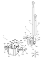
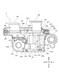
- FIG. 1 is a front perspective view of the capacitor module according to the first embodiment.
- FIG. 2 is a perspective view of the capacitor module showing a state before the assembly body is accommodated in the case according to the first embodiment.
- FIG. 3 is an exploded perspective view of the assembly body according to the first embodiment.
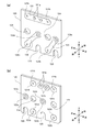
- 4A and 4B are a front perspective view and a rear perspective view of the relay board according to the first embodiment, respectively.
- FIG. 5A is a perspective view of the case according to the first embodiment as seen from above the front
- FIG. 5B is a perspective view of the case as seen from above the back according to the first embodiment.
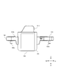
- FIG. FIG. 6 is a front view of the case according to the first embodiment.
- FIG. 7 is a plan view of the capacitor module according to the first embodiment before the case is filled with the filling resin.
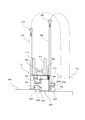
- FIG. 8 is a diagram illustrating a state in which the capacitor module is attached to an external attachment member according to the first embodiment.
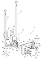
- FIG. 9 is a front perspective view of the capacitor module according to the second embodiment.
- FIG. 10 is a perspective view of the capacitor module showing a state before the assembly body is accommodated in the case according to the second embodiment.
- FIG. 11 is an exploded perspective view of the assembly body according to the second embodiment.
- FIGS. 12A and 12B are a front perspective view and a rear perspective view of the relay board according to the second embodiment, respectively.
- FIGS. 13A and 13B are a front perspective view and a rear perspective view of the case according to the second embodiment, respectively.
- FIG. 14 is a front view of a case according to the second embodiment.
- FIG. 15 is a plan view of the capacitor module according to the second embodiment before the case is filled with the filling resin.
- FIG. 16 is a diagram illustrating a state in which the capacitor module is attached to an external attachment member according to the second embodiment.
- the first lead wire 112 and the second lead wire 113 correspond to the “first lead wire” and the “second lead wire” recited in the claims, respectively.
- the first conductive pattern 121 corresponds to the “first conductive pattern” recited in the claims
- the second conductive pattern 122 and the third conductive pattern 123 correspond to the “second conductive pattern” recited in the claims.
- the first notch groove 125 and the second notch groove 126 correspond to “through holes” recited in the claims.
- the bus bar 130 corresponds to a “first connection terminal member” recited in the claims.
- the connection terminal 134 corresponds to a “first terminal portion” recited in the claims.
- first harness 140 and the second harness 150 correspond to a “second connection terminal member” recited in the claims.
- round crimp terminals 142 and 152 correspond to the “second terminal portion” recited in the claims.
- front surface 161b, the rear surface 161c, the left surface 161d, and the right surface 161e correspond to “four side surfaces” recited in the claims.
- first attachment tab 162 and the second attachment tab 163 correspond to a “fixing portion” recited in the claims.
- the first substrate holding unit 165 and the second substrate holding unit 166 correspond to the “substrate positioning unit” recited in the claims.
- bus bar holding portion 167 and the engagement rib 162b correspond to a “first terminal positioning portion” described in the claims.
- correspond to the "2nd terminal positioning part” as described in a claim.
- FIG. 1 is a front perspective view of the capacitor module 1 according to the first embodiment.
- FIG. 2 is a perspective view of the capacitor module 1 showing a state before the assembly A1 is accommodated in the case 160 according to the first embodiment.
- FIG. 3 is an exploded perspective view of the assembly A1 according to the first embodiment.
- 4A and 4B are respectively a front perspective view and a rear perspective view of the relay board 120 according to the first embodiment.
- FIG. 5A is a perspective view of the case 160 as viewed from the front upper side according to the first embodiment
- FIG. 5B is a case 160 as viewed from the upper rear side according to the first embodiment.
- FIG. FIG. 6 is a front view of the case 160 according to the first embodiment.
- FIG. 7 is a plan view of the capacitor module 1 according to the first embodiment before the case 160 is filled with the filling resin 170.
- FIG. 8 is a view showing a state in which the capacitor module 1 is attached to the external attachment member 180 according to the first embodiment.
- part of the filling resin 170 is drawn with diagonal lines, and the remaining part is drawn transparently.
- the capacitor module 1 includes two capacitors 110, a relay board 120, a bus bar 130, a first harness 140, and a second harness 150. Further, the capacitor module 1 is filled in a case 160 in which an assembly body A1 formed by integrating the capacitor 110, the relay board 120, the bus bar 130, the first harness 140, and the second harness 150 is accommodated. Filling resin 170.
- Capacitor 110 is connected to capacitor body 111 formed by coating the capacitor element with an outer package such as powder resin, and the first lead wire 112 and the second lead wire 112 connected to the electrodes at both ends of the capacitor element and drawn out from capacitor body 111 to the outside.
- Capacitor 110 can be, for example, a film capacitor.
- the capacitor element is formed, for example, by stacking two metallized films on which aluminum is vapor-deposited on a dielectric film, winding or stacking the stacked metallized films, and pressing them flatly.
- the first lead wire 112 and the second lead wire 113 are formed by plating a metal wire such as a copper wire with tin or the like. In the middle of these lead wires 112 and 113, lateral U-shaped bent portions 112a and 113a projecting inward are formed.
- the relay board 120 has a substantially rectangular shape, and its vertical and horizontal dimensions are slightly smaller than the vertical and horizontal dimensions inside the case 160.
- a first conductive pattern 121, a second conductive pattern 122, and a third conductive pattern 123 made of a metal foil such as a copper foil are formed on the front surface of the relay substrate 120.
- the first conductive pattern 121 extends in the left-right direction at the top of the relay substrate 120.
- two bus bar through holes 121a are formed so as to be arranged in the center, and capacitor through holes 121b are formed at both ends.
- the second conductive pattern 122 extends obliquely downward to the left from the center portion of the relay substrate 120.
- the second conductive pattern 122 has a harness through hole 122a at the upper end and a capacitor through hole 122b at the lower end.
- the third conductive pattern 123 extends obliquely downward to the left from the central portion of the right end of the relay substrate 120.
- a through hole 123a for a harness is formed at the upper end, and a through hole 123b for a capacitor is formed at the lower end.
- the bus bar through-hole 121a, the capacitor through-holes 121b, 122b, 123b and the harness through-holes 122a, 123a all include a metal foil such as a copper foil covering the inner peripheral surface of the hole or a metal plating such as copper plating. .
- bus bar lands 121c made of metal foil such as copper foil are disposed around the bus bar through holes 121a, the capacitor through holes 121b, 122b, 123b and the harness through holes 122a, 123a, respectively.
- Capacitor lands 121d, 122d, 123d and harness lands 122c, 123c are formed.
- Bus bar land 121c and capacitor land 121d are electrically connected to first conductive pattern 121 through bus bar through hole 121a and capacitor through hole 121b, respectively.
- Harness land 122c and capacitor land 122d are electrically connected to second conductive pattern 122 through harness through hole 122a and capacitor through hole 122b, respectively.
- the harness land 123c and the capacitor land 123d are electrically connected to the third conductive pattern 123 through the harness through hole 123a and the capacitor through hole 123b, respectively.
- circular circulation holes 124 are formed on the left and right sides of the harness through hole 122a. Further, the relay board 120 has a first notch groove 125 and a second notch groove 126 at the positions just below the harness through hole 122a and the harness through hole 123a so that the lower end is notched in an inverted U shape. Is formed.
- the bus bar 130 is formed by appropriately cutting and bending a conductive material, for example, a copper plate.
- the bus bar 130 has a bent portion 131 that is bent upward in a rectangular shape at the center.
- two terminal pins 132 are formed on the rear side so as to be lined up on the left and right sides, and an engagement piece 133 is formed on the front side so as to protrude forward.
- a circular connection terminal 134 having a mounting hole 134 a is formed at the distal end portion of the bus bar 130, and an engagement groove 135 that is recessed inward is formed at the front and rear root portions of the connection terminal 134.
- the first harness 140 includes a conductive wire 141 with an insulating coating, a round crimp terminal 142, and a protective tube 143.
- Conductive wire 141 with insulation coating (hereinafter abbreviated as “conductive wire 141”) is formed, for example, by coating a stranded wire made of a copper wire with a fluorine resin or the like.
- the round crimp terminal 142 is attached to the end of the conducting wire 141 opposite to the end connected to the relay substrate 120.
- the protective tube 143 covers a portion of the conducting wire 141 exposed from the case 160 and protects the conducting wire 141 from being damaged.
- the second harness 150 has the same configuration as the first harness 140, and includes a conductor 151 with insulation coating (hereinafter abbreviated as “conductor 151”), a round crimp terminal 152, and a protective tube 153.
- the length of the second harness 150 is shorter than the length of the first harness 140.
- the case 160 is formed of a resin material such as PPS and has a case body 161 having a substantially rectangular parallelepiped box shape with an upper surface opened, a first mounting tab 162 provided on the left side of the case body 161, and a right side of the case body 161. And a second mounting tab 163 provided.
- the case main body 161 has a square bottom surface 161a and four side surfaces of a front surface 161b, a rear surface 161c, a left surface 161d, and a right surface 161e that rise from the bottom surface 161a.
- a first substrate holding portion 165 and a second substrate holding portion 166 are formed on the left surface 161d and the right surface 161e, respectively.
- a first insertion groove 165a and a second insertion groove 166a extending in the vertical direction are formed in the first substrate holding part 165 and the second substrate holding part 166, respectively.
- the groove widths of the first insertion groove 165a and the second insertion groove 166a are substantially equal to the thickness of the relay substrate 120.
- a bus bar holding portion 167 extending in the vertical direction is formed on the front surface 161b.
- the bus bar holding portion 167 has an engagement recess 167a corresponding to the engagement piece 133 of the bus bar 130 at the upper end.
- first harness holding portion 168 and a second harness holding portion 169 are formed on the rear surface 161c so as to be arranged on the left and right.
- the first harness holding portion 168 has a pair of left and right holding ribs 168a and 168b extending in the vertical direction so as to face each other with a distance substantially equal to the width of the conductive wire 141 of the first harness 140.
- Reinforcing ribs 168c and 168d for reinforcing the holding ribs 168a and 168b are integrally formed below the holding ribs 168a and 168b.
- the second harness holding portion 169 includes a pair of left and right holding ribs 169a and 169b that extend in the vertical direction so as to face each other with an interval substantially equal to the width of the conducting wire 151 of the second harness 150.
- a reinforcing rib 169c for reinforcing the holding rib 169b is integrally formed under the right holding rib 169b.
- the rear surface 161c of the case body 161 is formed with a support portion 161f that extends upward from the upper end of the rear surface 161c.
- a circular mounting hole 162 a is formed in the first mounting tab 162.
- a metal collar 164 is fitted into the mounting hole 162a to increase the strength of the hole.
- engagement ribs 162b projecting upward are formed at the front end portion and the rear end portion closer to the case body 161 than the attachment hole 162a.
- a positioning pin 162c that protrudes downward is formed on the lower surface of the first mounting tab 162 behind the mounting hole 162a.
- the second mounting tab 163 is formed with a circular mounting hole 163a.
- the collar 164 is fitted into the mounting hole 163a similarly to the mounting hole 162a.
- a positioning pin 163b that protrudes downward is formed on the lower surface of the second mounting tab 163 to the right of the mounting hole 163a.
- the filling resin 170 is a thermosetting resin, for example, an epoxy resin.
- the filling resin 170 may be a urethane resin. As shown in FIG. 1, the filling resin 170 covers the main parts of the assembly A1, and protects these parts from moisture and impact.
- the capacitor module 1 When the capacitor module 1 is assembled, first, the two capacitors 110, the bus bar 130, the first harness 140, and the second harness 150 are attached to the relay board 120, as shown in FIG.
- the assembly body A1 is assembled. At this time, one capacitor 110 is inserted into the capacitor through-hole 121b at the left end of the first conductive pattern 121 until it stops at the bent portion 112a and soldered to the first conductive pattern 121.
- the second lead wire 113 is inserted into the capacitor through hole 122b of the second conductive pattern 122 until it stops at the bent portion 113a and connected to the second conductive pattern 122 by soldering.
- the other capacitor 110 is inserted into the capacitor through-hole 121b at the right end of the first conductive pattern 121 until it stops at the bent portion 112a and connected to the first conductive pattern 121 by soldering.
- the second lead wire 113 is inserted into the capacitor through hole 123b of the third conductive pattern 123 until it stops at the bent portion 113a, and is connected to the third conductive pattern 123 by soldering.
- two terminal pins 132 are inserted into the two bus bar through holes 121 a of the first conductive pattern 121 and connected to the first conductive pattern 121 by soldering.
- the end portion of the conductive wire 141 is inserted into the harness through hole 122a of the second conductive pattern 122 and connected to the second conductive pattern 122 by soldering.
- the second harness 150 is connected to the third conductive pattern 123 by soldering by inserting the end portion of the conductive wire 151 into the harness through hole 123 a of the third conductive pattern 123.
- first lead wire 112 of one capacitor 110 and the first lead wire 112 of the other capacitor 110 are electrically connected to the bus bar 130 via the first conductive pattern 121.
- the second lead wire 113 of one capacitor 110 is electrically connected to the first harness 140 via the second conductive pattern 122, and the second lead wire 113 of the other capacitor 110 is connected to the third conductive pattern 123. It is electrically connected to the second harness 150 via.
- the first harness 140 and the second harness 150 are respectively drawn through the first cutout groove 125 and the second cutout groove 126 of the relay board 120 to the rear side of the relay board 120.
- the assembled assembly A1 is inserted into the case 160 from above.
- the relay substrate 120 has the left end portion inserted into the first insertion groove 165 a of the first substrate holding portion 165 and the right end portion thereof the second insertion groove of the second substrate holding portion 166. It is inserted into 166b.
- the relay board 120 is positioned with respect to the case 160 and is held so as not to move in the front-rear and left-right directions in this state.
- the relay board 120 is spanned between the left surface 161d and the right surface 161e of the case 160, and is in a state of being stood with respect to the bottom surface 161a.
- the engagement piece 133 engages with the engagement recess 167 a of the bus bar holding portion 167, and the two engagement grooves 135 engage with the engagement ribs 162 b of the corresponding first mounting tabs 162. .
- the bus bar 130 is positioned with respect to the case 160 and is held so as not to move in the front-rear and left-right directions in this state.
- the mounting hole 134 a of the connection terminal 134 is aligned with the mounting hole 162 a of the first mounting tab 162.
- the first harness 140 is raised along the rear surface 161c of the case 160 so as to be sandwiched between the pair of holding ribs 168a and 168b of the first harness holding portion 168.
- the 1st harness 140 is positioned with respect to the case 160, and is hold
- the second harness 150 is raised along the rear surface 161c of the case 160 so as to be sandwiched between the pair of holding ribs 169a and 169b of the second harness holding portion 169.
- the second harness 150 is positioned with respect to the case 160 and is held so as not to move in the left-right direction in this state.
- maintenance part 169 are formed in the rear surface 161c facing the relay board
- the harnesses 140 and 150 are subjected to a force for spreading back and forth. For this reason, since the first harness 140 and the second harness 150 are pressed against the rear surface 161c of the case 160 by this force, the first harness 140 and the second harness 150 are connected to the first harness holding portion 168 and the second harness holding portion 169. It is hard to come off from the front.
- the first harness 140 is drawn upward from the case 160 at the position of the first harness holding part 168, and the second harness 150 is drawn upward from the case 160 at the position of the second harness holding part 169.
- the pulled-out first harness 140 and second harness 150 are supported on the rear side by a support portion 161f.
- the liquid filling resin 170 is injected into the case 160, and the filling resin 170 is filled into the case 160 up to a position where the two capacitors 110 and the relay substrate 120 are buried. .
- the two circulation holes 124, the first cutout groove 125, and the second cutout groove 126 are formed in the relay board 120, one of the two spaces in the case 160 partitioned by the relay board 120.
- the filled resin 170 poured into this space can flow into the other space through the flow hole 124, the first notch groove 125 and the second notch groove 126. Thereby, the filling resin 170 can be smoothly spread over the entire case 160.
- the liquid filling resin 170 is cured.
- the capacitor module 1 is completed.
- the assembly A1 is fixed by the cured filling resin 170 and cannot be removed upward from the case 160.
- the capacitor module 1 is mounted on a device or a vehicle. At this time, for example, as shown in FIG. 8, the capacitor module 1 is attached to an attachment member 180 prepared for a device or a vehicle.
- the attachment member 180 is made of a metal such as aluminum and has a first attachment boss 181 and a second attachment boss 182.
- the capacitor module 1 is fixed to the attachment member 180 by attaching the first attachment tab 162 to the first attachment boss 181 with the screw 183 and attaching the second attachment tab 163 to the second attachment boss 182 with the screw 184. .
- the positioning pin 162c of the first mounting tab 162 is inserted into the positioning hole 181a of the first mounting boss 181 and the positioning pin 163b of the second mounting tab 163 is inserted into the positioning hole 182a of the second mounting boss 182.
- the capacitor module 1 is fixed to the mounting member 180 in an appropriate direction.
- the bus bar 130 is electrically connected to the first mounting boss 181 through the screw 184.
- the first harness 140 and the second harness 150 are connected to the connection terminals 191 and 192 of an electric circuit unit such as an inverter circuit and a power circuit, in which the round crimp terminals 142 and 152 are arranged separately from the mounting member 180. Electrically connected.
- the first lead wire 112 of the capacitor 110 is electrically connected to the bus bar 130 via the first conductive pattern 121 of the relay substrate 120, and the second lead wire 113 of the capacitor 110 is second conductive. It is electrically connected to the first harness 140 (second harness 150) via the pattern 122 (third conductive pattern 123). The connection of the first lead wire 112 and the second lead wire 113 to the first conductive pattern 121 and the second conductive pattern 122 (third conductive pattern 123) by soldering is performed when the capacitor is mounted on a normal printed circuit board.
- the capacitor main body 111 is unlikely to become high temperature due to heat of soldering. Therefore, the lead wire (lead terminal) type capacitor 110 is electrically connected to a connection portion such as an external connection terminal using the bus bar 130 or the first harness 140 (second harness 150) while suppressing damage due to heat. Can be connected.
- An assembly A1 in which the capacitor 110, the relay board 120, the bus bar 130, and the first harness 140 (second harness 150) are integrated is accommodated in the case 160, and the relay board 120, the bus bar 130, and the first harness 140 (second harness 140).
- Each of the harnesses 150) is positioned relative to the case 160.
- the bus bar 130 and the first harness 140 (second harness 150) can be pulled out from the determined position of the case 160 with high accuracy.
- the bus bar 130 and the first harness 140 (second harness 150) can be accurately placed at a predetermined position of the installation destination.
- the bus bar 130 and the first harness 140 (second harness 150) can be smoothly connected to a connection portion such as a connection terminal at the installation destination. Further, it is possible to prevent the bus bar 130 and the first harness 140 (second harness 150) from interfering with other components at the installation destination.
- the first harness holding portion 168 (second harness holding portion 169) has a structure in which the first harness 140 (second harness 150) is sandwiched between two holding ribs 168a, 168b (169a, 169b). When accommodated in the case 160, the first harness 140 (second harness 150) can be easily attached to the first harness holding portion 168 (second harness holding portion 169). In addition, since the first harness holding portion 168 (second harness holding portion 169) is formed on the rear surface 161c facing the relay substrate 120 in the case 160, it is bent between the relay substrate 120 and the rear surface 161c.
- the first harness 140 (second harness 150) has a second conductive pattern 122 (third conductive pattern 123) on the front side of the relay board 120 that does not face the first harness holding portion 168 (second harness holding portion 169). Is connected to the first harness 140 (second harness 150) until the first harness holding part 168 (second harness holding part 169) reaches the first notch groove 125 (first 2 is passed through the notch 126). As a result, the movement of the first harness 140 (second harness 150) can be restricted by the first notch groove 125 (second notch groove 126), so that the first harness 140 (second harness 150) is difficult to move in the case 160. Become.
- the capacitor module 2 according to the second embodiment will be described with reference to FIGS. 9 to 16.
- front and rear, left and right, and up and down directions are appropriately appended to each drawing.
- the direction of illustration shows the relative direction of the capacitor
- the first lead wire 212 and the second lead wire 213 correspond to the “first lead wire” and the “second lead wire” recited in the claims, respectively.
- the first conductive pattern 221 corresponds to the “first conductive pattern” recited in the claims
- the second conductive pattern 222 and the third conductive pattern 223 are defined in the “second conductive pattern”.
- the notch groove 225 corresponds to a “through hole” described in the claims.
- the first bus bar 230 corresponds to a “first connection terminal member” recited in the claims.
- the connection terminal 234 corresponds to a “first terminal portion” recited in the claims.
- the second bus bar 240 and the third bus bar 250 correspond to a “second connection terminal member” recited in the claims.
- connection terminals 244 and 257 correspond to a “second terminal portion” recited in the claims.
- the first harness 260 and the second harness 270 correspond to a “third connection terminal member” recited in the claims.
- the round crimp terminals 262 and 272 correspond to the “third terminal portion” recited in the claims.
- the first attachment tab 282 and the second attachment tab 283 correspond to a “fixing portion” recited in the claims.
- the first substrate holding unit 285 and the second substrate holding unit 286 correspond to the “substrate positioning unit” recited in the claims.
- the engagement rib 282b corresponds to a “first terminal positioning portion” recited in the claims.
- the first engagement recess 287 and the second engagement recess 288 correspond to a “second terminal positioning portion” recited in the claims.
- correspond to the "3rd terminal positioning part" as described in a claim.
- FIG. 9 is a front perspective view of the capacitor module 2 according to the second embodiment.
- FIG. 10 is a perspective view of the capacitor module 2 according to the second embodiment showing a state before the assembly A2 is accommodated in the case 280.
- FIG. 11 is an exploded perspective view of the assembly A2 according to the second embodiment.
- 12A and 12B are respectively a front perspective view and a rear perspective view of the relay board 220 according to the second embodiment.
- FIGS. 13A and 13B are a front perspective view and a rear perspective view, respectively, of the case 280 according to the second embodiment.
- FIG. 14 is a front view of the case 280 according to the second embodiment.
- FIG. 15 is a plan view of the capacitor module 2 before the case 280 is filled with the filling resin 290 according to the second embodiment.
- FIG. 16 is a diagram illustrating a state in which the capacitor module 2 is attached to the external attachment member 300 according to the second embodiment.
- part of the filling resin 290 is drawn with diagonal lines, and the remaining part is drawn transparently.
- the capacitor module 2 includes two capacitors 210, a relay substrate 220, a first bus bar 230, a second bus bar 240, a third bus bar 250, a first harness 260, and a second harness 270. Further, the capacitor module 2 accommodates an assembly A2 in which the capacitor 210, the relay board 220, the first bus bar 230, the second bus bar 240, the third bus bar 250, the first harness 260, and the second harness 270 are integrated. Case 280 and a filling resin 290 filled in the case 280.
- the capacitor 210 has the same configuration as the capacitor 110 of the first embodiment, and includes a capacitor body 211, a first lead wire 212 having a bent portion 212a, and a second lead wire 213 having a bent portion 213a. including.
- the relay board 220 has a substantially rectangular shape, and the vertical and horizontal dimensions thereof are slightly smaller than the vertical and horizontal dimensions inside the case 280.
- a first conductive pattern 221, a second conductive pattern 222, and a third conductive pattern 223 made of a metal foil such as a copper foil are formed on the front surface of the relay substrate 220.
- the first conductive pattern 221 extends in the vertical direction at the right end of the relay substrate 220.
- the first conductive pattern 221 two through holes for bus bars 221a are formed so as to be lined up on the left and right at the upper end, and two through holes for capacitors 221b are arranged in the vertical direction below the through holes for bus bars 221a. It is formed.
- the second conductive pattern 222 is located at the upper part of the right end portion of the relay substrate 220.
- two through holes 222a for bus bars are formed so as to be aligned vertically on the left side, and a through hole 222b for harness and a through hole 222c for capacitors are formed so as to be aligned vertically on the right side.
- the third conductive pattern 223 is located below the right end portion of the relay substrate 220.
- two through holes for bus bars 223a are formed so as to be lined up and down on the left side, and a through hole for capacitors 223c and a through hole for harness 223b are formed so as to be lined up and down on the right side.
- the bus bar through holes 221a, 222a, 223a, the capacitor through holes 221b, 222c, 223c and the harness through holes 222b, 223b are all made of metal foil such as copper foil covering the inner peripheral surface of the hole or copper plating. Includes metal plating.
- bus bars made of metal foil such as copper foil are provided around the through holes 221a, 222a, 223a for the bus bars, the through holes 221b, 222c, 223c for the capacitors, and the through holes 222b, 223b for the harnesses.
- Lands 221c, 222d, 223d for capacitors, 221d, 222f, 223f for capacitors, and lands 222e, 223e for harnesses are formed.
- Bus bar land 221c and capacitor land 221d are electrically connected to first conductive pattern 221 through bus bar through hole 221a and capacitor through hole 221b, respectively.
- bus bar land 222d, the harness land 222e, and the capacitor land 222f are electrically connected to the second conductive pattern 222 through the bus bar through hole 222a, the harness through hole 222b, and the capacitor through hole 222c, respectively.
- Bus bar land 223d, harness land 223e, and capacitor land 223f are electrically connected to third conductive pattern 223 through bus bar through hole 223a, harness through hole 223b, and capacitor through hole 223c, respectively. .
- the relay substrate 220 In the relay substrate 220, four circular flow holes 224 are formed between the three conductive patterns 221, 222, and 223. Furthermore, a cutout groove 225 is formed in the relay substrate 220 so as to cut out the center portion of the lower end portion in an inverted U shape.
- the first bus bar 230 is formed by appropriately cutting and bending a conductive material, for example, a copper plate.
- the 1st bus-bar 230 has the bending part 231 bent in the rectangular shape toward the upper part in the center part.
- two terminal pins 232 are formed on the right side so as to be arranged in the front-rear direction, and an opening 233 is formed on the left side of the terminal pins 232.
- a circular connection terminal 234 having a mounting hole 234a is formed at the distal end portion of the first bus bar 230, and an engagement groove 235 that is recessed inward is formed at the front and rear base portions of the connection terminal 234.
- the second bus bar 240 is formed by appropriately cutting and bending a conductive material, for example, a copper plate.
- the second bus bar 240 has a bent portion 241 bent rearward at the center.
- two terminal pins 242 are formed on the right side so as to be lined up and down, and an opening 243 is formed on the left side of the terminal pins 242.
- a square connection terminal 244 having a mounting hole 244a is formed at the tip of the second bus bar 240.
- the third bus bar 250 is formed by appropriately cutting and bending a conductive material, for example, a copper plate.
- the third bus bar 250 has a bent portion 251 at the center, which is bent upward and then bent upward, and extends slightly upward and then bent backward.
- An attachment terminal 252 extending rightward is formed at the base end portion of the third bus bar 250.
- the attachment terminal 252 is formed with two terminal pins 253 arranged vertically at the tip, and an opening 254 is formed on the left side of the terminal pin 253.
- a first harness holding portion 255 is further formed on the left side, and a second harness holding portion 256 is formed on the lower side.
- the first harness holding portion 255 has a U-shape that opens rearward.
- the second harness holding portion 256 has a structure in which a first holding piece 256a that extends straight downward and a second holding piece 256b that extends downward and extends downward are arranged side by side. Furthermore, a rectangular connection terminal 257 having a mounting hole 257 a is formed at the tip of the third bus bar 250.
- the first harness 260 has the same configuration as the first harness 140 of the first embodiment, and includes a conductive wire 261 with insulation coating (hereinafter abbreviated as “conductive wire 261”), a round crimp terminal 262, and a protective tube. H.263.
- the second harness 270 includes a conductive wire 271 with insulation coating (hereinafter abbreviated as “conductive wire 271”), a round crimp terminal 272, and a protective tube 273.
- the 2nd harness 270 in order for the part hold
- the length of the second harness 270 is made shorter than the length of the first harness 260.
- the case 280 is formed of a resin material such as PPS and has a box-like case main body 281 having an upper surface opened, a first attachment tab 282 provided on the left side of the case main body 281, and a first main body provided on the right side of the case main body 281. 2 mounting tabs 283.
- the case main body 281 has a substantially horizontal L shape in plan view.
- a first substrate holding portion 285 and a second substrate holding portion 286 are formed at the right end portions of the front surface 281 a and the rear surface 281 b, respectively.
- a first insertion groove 285a and a second insertion groove 286a extending in the vertical direction are formed in the first substrate holding part 285 and the second substrate holding part 286, respectively.
- the groove widths of the first insertion groove 285a and the second insertion groove 286a are substantially equal to the thickness of the relay substrate 220.
- a first engagement recess 287 and a second engagement recess 288 that are slightly recessed are formed on the right side and the left side, respectively, at the upper end of the rear surface 281b.
- the width of the first engaging recess 287 is substantially equal to the width of the bent portion 241 of the second bus bar 240, and the width of the second engaging recess 288 is substantially equal to the width of the bent portion 251 of the third bus bar 250.
- a harness holding portion 289 is formed at the right rear end portion of the case main body 281.
- the harness holding portion 289 forms an accommodation space 289a that can accommodate the first harness 260 by expanding the right rear end portion of the case main body 281 to the right, and a part of the entrance to the accommodation space 289a extends vertically.
- the structure is closed by the closing rib 289b.
- a positioning pin 281 c that protrudes downward is formed on the outer bottom surface of the case body 281.
- a circular mounting hole 282a is formed in the first mounting tab 282.
- a metal collar 284 is fitted into the mounting hole 282a in order to increase the strength of the hole.
- an engaging rib 282b protruding upward is formed at the front end portion and the rear end portion on the right side of the mounting hole 282a.
- a circular mounting hole 283a is formed in the second mounting tab 283.
- a collar 284 is fitted into the mounting hole 283a as well as the mounting hole 282a.
- a positioning pin 283b protruding downward is formed on the lower surface of the second mounting tab 283 in front of the mounting hole 283a.
- the filling resin 290 is a thermosetting resin, for example, an epoxy resin.
- the filling resin 290 may be a urethane resin. As shown in FIG. 9, the filling resin 290 covers the main parts of the assembly A2 and protects these parts from moisture and impact.
- the capacitor module 2 When the capacitor module 2 is assembled, first, the two capacitors 210, the first bus bar 230, the second bus bar 240, the third bus bar 250, the first harness 260, and the second harness 270 are relayed. By attaching to the substrate 220, the assembly A2 is assembled as shown in FIG. At this time, one capacitor 210 is inserted into the capacitor through hole 221b on the upper side of the first conductive pattern 221 until it stops at the bent portion 212a, and is soldered to the first conductive pattern 221. The second lead wire 213 is inserted into the capacitor through hole 222c of the second conductive pattern 222 until it stops at the bent portion 213a and connected to the second conductive pattern 222 by soldering.
- the other capacitor 210 is inserted into the capacitor through hole 221b on the lower side of the first conductive pattern 221 until the first lead wire 212 stops at the bent portion 212a, and is soldered to the first conductive pattern 221.
- the second lead wire 213 is inserted into the capacitor through hole 223c of the third conductive pattern 223 until it stops at the bent portion 213a and connected to the third conductive pattern 223 by soldering.
- two terminal pins 232 are inserted into the two through holes 221 a for the bus bar of the first conductive pattern 221 and connected to the first conductive pattern 221 by soldering.
- the second bus bar 240 two terminal pins 242 are inserted into the two through holes 222 a for the bus bar of the second conductive pattern 222 and connected to the second conductive pattern 222 by soldering.
- the third bus bar 250 two terminal pins 253 are inserted into the two bus bar through holes 223 a of the third conductive pattern 223 and connected to the third conductive pattern 223 by soldering.
- the first harness 260 is connected to the second conductive pattern 222 by soldering by inserting the end portion of the conducting wire 261 into the harness through hole 222b of the second conductive pattern 222.
- the second harness 270 is connected to the third conductive pattern 223 by soldering with the end portion of the conducting wire 271 being inserted into the harness through hole 223b of the third conductive pattern 223.
- first lead wire 212 of one capacitor 210 and the first lead wire 212 of the other capacitor 210 are electrically connected to the first bus bar 230 via the first conductive pattern 221.
- second lead 213 of one capacitor 210 is electrically connected to the second bus bar 240 and the first harness 260 via the second conductive pattern 222
- the second lead 213 of the other capacitor 210 is The third bus bar 250 and the second harness 270 are electrically connected through the third conductive pattern 223.
- the first harness 260 is rotated around the two capacitors 210, the first harness 260 is passed through the notch groove 225 of the relay board 220 and pulled out to the right side of the relay board 220.
- the second harness 270 extends leftward from the relay board 220, the second harness 270 is held by the second harness holding portion 256 so as to be sandwiched between the first holding piece 256a and the second holding piece 256b. .
- the second harness 270 is further bent upward and held by the first harness holding portion 255 so as to be fitted into the U-shaped portion.
- the second harness 270 is positioned with respect to the third bus bar 250 by being held by the first harness holding portion 255 and the second harness holding portion 256.
- the assembled assembly A2 is inserted into the case 280 from above.
- the relay substrate 220 has its right end inserted into the first insertion groove 285 a of the first substrate holding portion 285 and its left end as the second difference of the second substrate holding portion 286. It is inserted into the insertion groove 286a.
- the relay substrate 220 is positioned with respect to the case 280 and is held so as not to move in the front-rear and left-right directions in this state.
- the relay board 220 is spanned between the front surface 281a and the rear surface 281b of the case 280, and is accommodated in the case 280 in a standing state.
- the two engagement grooves 235 are engaged with the engagement ribs 282b of the first mounting tabs 282 corresponding to the two engagement grooves 235, respectively. Accordingly, the first bus bar 230 is positioned with respect to the case 280 and is held so as not to move in the front-rear and left-right directions in this state. In the first bus bar 230, the attachment hole 234 a of the connection terminal 234 is aligned with the attachment hole 282 a of the first attachment tab 282.
- the bent portions 241 and 251 of the second bus bar 240 and the third bus bar 250 engage with the first engaging recess 287 and the second engaging recess 288, respectively.
- the 2nd bus bar 240 and the 3rd bus bar 250 are positioned with respect to case 280, and are held so that it may not move in the horizontal direction in this state.
- the first harness 260 is raised so as to be accommodated in the accommodating space 289 a of the harness holding portion 289.
- the 1st harness 260 is positioned with respect to case 280, and is hold
- the second bus bar 240 is drawn upward from the case 280 at the position of the first engagement recess 287
- the third bus bar 250 is drawn upward from the case 280 at the position of the second engagement recess 288.
- the first harness 260 is drawn upward from the case 280 at the position of the harness holding portion 289
- the second harness 270 is drawn upward from the case 280 at the position of the first harness holding portion 255 of the third bus bar 250. .
- the liquid filling resin 290 is injected into the case 280, and the filling resin 290 is filled into the case 280 up to a position where the two capacitors 210 and the relay substrate 220 are buried. .
- the filling resin 290 injected into the case 280 passes through the four through holes 224 and the notch groove 225 formed in the relay substrate 220, so that a space between the relay substrate 220 and the right surface 281 d of the case 280 is obtained. Easy to get around.
- the injected filling resin 290 easily reaches the lower portion of the first bus bar 230 by passing through the opening 233 of the first bus bar 230.
- the injected filling resin 290 easily reaches the rear of the second bus bar 240 and the third bus bar 250 by passing through the opening 243 of the second bus bar 240 and the opening 254 of the third bus bar 250.
- the case 280 When the case 280 is heated after the case 280 is filled with the filling resin 290, the liquid filling resin 290 is cured. Thus, the capacitor module 2 is completed. In the case 280, the assembly A2 is fixed with the cured filling resin 290, and cannot be removed upward from the case 280.
- the capacitor module 2 is also mounted on a device, a vehicle, or the like, like the capacitor module 1 of the first embodiment. At this time, the capacitor module 2 is attached to an attachment member 300 prepared in a device, a vehicle, or the like, for example, as shown in FIG.
- the attachment member 300 is made of a metal such as aluminum and has a first attachment boss 301 and a second attachment boss 302.
- the capacitor module 2 is fixed to the attachment member 300 by attaching the first attachment tab 282 to the first attachment boss 301 with the screw 303 and attaching the second attachment tab 283 to the second attachment boss 302 with the screw 304. .
- the positioning pin 281c on the outer bottom surface of the case 280 is inserted into the positioning hole 300a of the mounting member 300, and the positioning pin 283b of the second mounting tab 283 is inserted into the positioning hole 302a of the second mounting boss 302.
- the capacitor module 2 is fixed to the mounting member 300 in an appropriate direction.
- the first bus bar 230 is electrically connected to the first mounting boss 301 through the screw 303.
- the first harness 260 and the second harness 270 are connected to the connection terminals 311 and 312 of an electric circuit unit such as an inverter circuit and a power supply circuit in which the round crimp terminals 262 and 272 are arranged separately from the attachment member 300. Electrically connected.
- the second bus bar 240 and the third bus bar 250 are electrically connected to harnesses 313 and 314 drawn from the electric circuit unit.
- the lead wire (lead terminal) type capacitor 210 is used to suppress damage due to heat while the first bus bar 230, the second bus bar 240 (third bus bar 250), and the first harness 260 (first 2 harness 270), and can be electrically connected to a connection portion such as an external connection terminal.
- the first bus bar 230, the second bus bar 240 (third bus bar 250), and the first harness 260 (second harness 270) are smoothly connected to a connection portion such as a connection terminal at the installation destination. Can do. Moreover, it can prevent that the 1st bus bar 230, the 2nd bus bar 240 (3rd bus bar 250), and the 1st harness 260 (2nd harness 270) interfere with the other components of an installation place.
- the third bus bar 250 is provided with a first harness holding portion 255 and a second harness holding portion 256, and the second harness 270 is held by the harness holding portions 255 and 256 so that the second harness 270 is third. Since the positioning is performed with respect to the bus bar 250, the case 280 is determined in the same manner as the first harness 260 and the like even if the case 280 is not provided with a structure for positioning the second harness 270. It can be accurately extracted from the position.
- the filling hole 224 formed in the relay substrate 220 smoothly fills the filled resin 290 poured into one space partitioned by the relay substrate 220 in the case 280 into the other space. Can be spread.
- connection terminal members such as the second bus bar 240 (third bus bar 250) and the first harness 260 (second harness 270) are electrically connected to the second lead wire 213 of the capacitor 210, that is, one lead wire. Therefore, one electrode side of the capacitor 110 can be connected to connection parts such as a plurality of external connection terminals using a plurality of connection terminal members.
- the capacitor modules 1 and 2 are provided with two capacitors 110 and 210.
- the capacitor modules 1 and 2 may have any number of capacitors 110 and 210.
- the bus bar 130 may be replaced with a harness
- the first harness 140 and the second harness 150 may be replaced with a bus bar.
- the first bus bar 230 may be replaced with a harness
- the set of the second bus bar 240 and the first harness 260 or the set of the third bus bar 250 and the second harness 270 is 2 It may be replaced with a set of two bus bars or a set of two harnesses.
- the connection terminal member connected to the capacitors 110 and 210 via the relay boards 120 and 220 may be changed as appropriate.
- the through holes such as the bus bar through holes 121a and 221a of the relay boards 120 and 220 are covered with metal plating such as metal foil or copper plating on the inner peripheral surface thereof. Lands such as bus bar lands 121c and 221c were formed on the rear surfaces of the relay boards 120 and 220. In such a configuration, the capacitors 110 and 210 can be firmly fixed to the relay boards 120 and 220 by soldering.
- the through holes are not necessarily covered with metal plating such as metal foil or copper plating, and lands may not be formed on the rear surfaces of the relay substrates 120 and 220.
- connection terminal members such as bus bars and harnesses
- the structure for positioning connection terminal members such as bus bars and harnesses with respect to the case is not limited to the structure used in the first and second embodiments, and may be any structure.
- capacitors 110 and 210 may be capacitors other than film capacitors, for example, electrolytic capacitors.
- the terms indicating directions such as “upward” and “downward” indicate relative directions that depend only on the relative positional relationship of the constituent members, and include vertical and horizontal directions. It does not indicate the absolute direction.
- the present invention is useful for capacitors used in various electronic equipment, electrical equipment, industrial equipment, vehicle electrical equipment, and the like.
Landscapes
- Engineering & Computer Science (AREA)
- Power Engineering (AREA)
- Microelectronics & Electronic Packaging (AREA)
- Manufacturing & Machinery (AREA)
- Details Of Connecting Devices For Male And Female Coupling (AREA)
- Fixed Capacitors And Capacitor Manufacturing Machines (AREA)
- Connection Or Junction Boxes (AREA)
- Multi-Conductor Connections (AREA)
- Structures For Mounting Electric Components On Printed Circuit Boards (AREA)
Abstract
La présente invention concerne un module de condensateur (1) qui comporte : un condensateur (110) qui comprend un corps principal (111) de condensateur, et un premier fil conducteur (112) et un deuxième fil conducteur (113) qui sortent du corps principal (111) de condensateur ; un substrat de relais (120) qui comporte un premier motif conducteur (121) auquel le premier fil conducteur (112) est électriquement connecté et un deuxième motif conducteur (122) auquel le deuxième fil conducteur (113) est électriquement connecté ; une barre omnibus (130) qui est électriquement connectée au premier motif conducteur (121) et dont une borne de connexion (134) est électriquement connectée à une partie de connexion externe ; et un premier faisceau (140) qui est électriquement connecté au deuxième motif conducteur (122) et dont une borne à sertissure ronde (142) est électriquement connectée à une partie de connexion externe.
Priority Applications (3)
| Application Number | Priority Date | Filing Date | Title |
|---|---|---|---|
| CN201780032162.5A CN109313982B (zh) | 2016-05-31 | 2017-05-18 | 电容器模块 |
| JP2018520789A JP7022898B2 (ja) | 2016-05-31 | 2017-05-18 | コンデンサモジュール |
| US16/190,375 US10629380B2 (en) | 2016-05-31 | 2018-11-14 | Capacitor module |
Applications Claiming Priority (2)
| Application Number | Priority Date | Filing Date | Title |
|---|---|---|---|
| JP2016-108169 | 2016-05-31 | ||
| JP2016108169 | 2016-05-31 |
Related Child Applications (1)
| Application Number | Title | Priority Date | Filing Date |
|---|---|---|---|
| US16/190,375 Continuation US10629380B2 (en) | 2016-05-31 | 2018-11-14 | Capacitor module |
Publications (1)
| Publication Number | Publication Date |
|---|---|
| WO2017208836A1 true WO2017208836A1 (fr) | 2017-12-07 |
Family
ID=60477753
Family Applications (1)
| Application Number | Title | Priority Date | Filing Date |
|---|---|---|---|
| PCT/JP2017/018613 Ceased WO2017208836A1 (fr) | 2016-05-31 | 2017-05-18 | Module de condensateur |
Country Status (4)
| Country | Link |
|---|---|
| US (1) | US10629380B2 (fr) |
| JP (1) | JP7022898B2 (fr) |
| CN (1) | CN109313982B (fr) |
| WO (1) | WO2017208836A1 (fr) |
Cited By (2)
| Publication number | Priority date | Publication date | Assignee | Title |
|---|---|---|---|---|
| JPWO2018016349A1 (ja) * | 2016-07-21 | 2019-05-16 | パナソニックIpマネジメント株式会社 | コンデンサ |
| JP2020031139A (ja) * | 2018-08-22 | 2020-02-27 | 株式会社指月電機製作所 | コンデンサ |
Families Citing this family (4)
| Publication number | Priority date | Publication date | Assignee | Title |
|---|---|---|---|---|
| WO2019107128A1 (fr) * | 2017-11-29 | 2019-06-06 | パナソニックIpマネジメント株式会社 | Condensateur |
| DE102019120334A1 (de) * | 2019-07-26 | 2021-01-28 | Jheeco E-Drive Ag | Kondensatorgehäuse und Zwischenkreiskondensator mit einem derartigen Gehäuse |
| DE102023211385A1 (de) * | 2023-11-16 | 2025-05-22 | Zf Friedrichshafen Ag | Kondensator, insbesondere Zwischenkreiskondensator, für eine Leistungselektronik eines Fahrzeugs |
| USD1120880S1 (en) * | 2024-05-31 | 2026-03-31 | Vishay Israel Ltd. | Base for a capacitor |
Citations (5)
| Publication number | Priority date | Publication date | Assignee | Title |
|---|---|---|---|---|
| JPS481975U (fr) * | 1971-05-25 | 1973-01-11 | ||
| JPS62184724U (fr) * | 1986-05-15 | 1987-11-24 | ||
| JP2013219110A (ja) * | 2012-04-05 | 2013-10-24 | Shizuki Electric Co Inc | コンデンサ |
| JP2014086628A (ja) * | 2012-10-25 | 2014-05-12 | Shizuki Electric Co Inc | コンデンサ |
| JP2014170882A (ja) * | 2013-03-05 | 2014-09-18 | Shizuki Electric Co Inc | コンデンサ |
Family Cites Families (8)
| Publication number | Priority date | Publication date | Assignee | Title |
|---|---|---|---|---|
| JPS5550993Y2 (fr) * | 1974-04-24 | 1980-11-27 | ||
| JP3054949B1 (ja) | 1999-03-31 | 2000-06-19 | 岡谷電機産業株式会社 | ケース収納型電子部品及びその製造方法 |
| JP4859443B2 (ja) * | 2005-11-17 | 2012-01-25 | 日立オートモティブシステムズ株式会社 | 電力変換装置 |
| JP5945710B2 (ja) * | 2011-10-28 | 2016-07-05 | パナソニックIpマネジメント株式会社 | キャパシタモジュール |
| US9947467B2 (en) * | 2012-04-25 | 2018-04-17 | Mjg Innovations, Llc | Protected capacitor system and method |
| KR101436787B1 (ko) * | 2013-12-31 | 2014-09-11 | 주식회사 뉴인텍 | 하우징 내장형 자동차 인버터용 저 인덕턴스 커패시터 |
| CN108701541A (zh) * | 2016-02-25 | 2018-10-23 | 松下知识产权经营株式会社 | 电容器 |
| CN109155195B (zh) * | 2016-05-25 | 2020-10-30 | 松下知识产权经营株式会社 | 电容器 |
-
2017
- 2017-05-18 WO PCT/JP2017/018613 patent/WO2017208836A1/fr not_active Ceased
- 2017-05-18 CN CN201780032162.5A patent/CN109313982B/zh active Active
- 2017-05-18 JP JP2018520789A patent/JP7022898B2/ja active Active
-
2018
- 2018-11-14 US US16/190,375 patent/US10629380B2/en active Active
Patent Citations (5)
| Publication number | Priority date | Publication date | Assignee | Title |
|---|---|---|---|---|
| JPS481975U (fr) * | 1971-05-25 | 1973-01-11 | ||
| JPS62184724U (fr) * | 1986-05-15 | 1987-11-24 | ||
| JP2013219110A (ja) * | 2012-04-05 | 2013-10-24 | Shizuki Electric Co Inc | コンデンサ |
| JP2014086628A (ja) * | 2012-10-25 | 2014-05-12 | Shizuki Electric Co Inc | コンデンサ |
| JP2014170882A (ja) * | 2013-03-05 | 2014-09-18 | Shizuki Electric Co Inc | コンデンサ |
Cited By (3)
| Publication number | Priority date | Publication date | Assignee | Title |
|---|---|---|---|---|
| JPWO2018016349A1 (ja) * | 2016-07-21 | 2019-05-16 | パナソニックIpマネジメント株式会社 | コンデンサ |
| JP7050229B2 (ja) | 2016-07-21 | 2022-04-08 | パナソニックIpマネジメント株式会社 | コンデンサ |
| JP2020031139A (ja) * | 2018-08-22 | 2020-02-27 | 株式会社指月電機製作所 | コンデンサ |
Also Published As
| Publication number | Publication date |
|---|---|
| CN109313982B (zh) | 2021-04-16 |
| US10629380B2 (en) | 2020-04-21 |
| JPWO2017208836A1 (ja) | 2019-04-04 |
| JP7022898B2 (ja) | 2022-02-21 |
| CN109313982A (zh) | 2019-02-05 |
| US20190080844A1 (en) | 2019-03-14 |
Similar Documents
| Publication | Publication Date | Title |
|---|---|---|
| JP7022898B2 (ja) | コンデンサモジュール | |
| JP5714716B2 (ja) | 電源制御装置 | |
| JP4055662B2 (ja) | 電気接続箱 | |
| JP3815154B2 (ja) | 電気接続箱 | |
| CN108028520A (zh) | 电路结构体及电连接箱 | |
| WO2011109741A1 (fr) | Système de support à faible coût de carte de circuit imprimé et de connectivité destiné à des circuits électroniques enfermés dans une enceinte | |
| TWI261389B (en) | Conductor connection module for printed circuit boards | |
| CN113196427B (zh) | 电容器 | |
| JP3772304B2 (ja) | プリント基板の相互間接続構造 | |
| CN101783447B (zh) | 电子产品的端子结构 | |
| CN104126333B (zh) | 包括印制电路板、单独电路板和电源连接器的电气和/或电子电路 | |
| US20180370460A1 (en) | Electronic component unit, wire harness, and connector fixing structure | |
| US10166869B1 (en) | Electronic component unit, wire harness, and connector fixing structure | |
| US20110256770A1 (en) | Receptacle for Electronic Devices | |
| JP5381617B2 (ja) | 電気接続箱 | |
| JP6808374B2 (ja) | 電子装置 | |
| RU240313U1 (ru) | Переходная плата для установки микросхем в корпусе SSOP-14 с обратной стороны посадочного места DIP-14 на основной печатной плате | |
| RU240499U1 (ru) | Переходная плата для установки микросхем в корпусе SOP-30 с обратной стороны посадочного места DIP-30 на основной печатной плате | |
| RU240889U1 (ru) | Переходная плата для установки микросхем в корпусе SSOP-32 с обратной стороны посадочного места DIP-32 на основной печатной плате | |
| CN1985416A (zh) | 互连连接器 | |
| JP6350867B2 (ja) | バスバー回路体の電子部品実装構造 | |
| JP5497389B2 (ja) | 電気接続箱 | |
| EP2808961A1 (fr) | Barre bus | |
| KR100997719B1 (ko) | 전자기기용 전원공급장치 | |
| KR20060052497A (ko) | 프린트 배선판용 커넥터 |
Legal Events
| Date | Code | Title | Description |
|---|---|---|---|
| ENP | Entry into the national phase |
Ref document number: 2018520789 Country of ref document: JP Kind code of ref document: A |
|
| NENP | Non-entry into the national phase |
Ref country code: DE |
|
| 121 | Ep: the epo has been informed by wipo that ep was designated in this application |
Ref document number: 17806394 Country of ref document: EP Kind code of ref document: A1 |
|
| 122 | Ep: pct application non-entry in european phase |
Ref document number: 17806394 Country of ref document: EP Kind code of ref document: A1 |