WO2017208914A1 - 液晶パネル、スイッチャブル・ミラーパネル及びスイッチャブル・ミラーディスプレイ - Google Patents
液晶パネル、スイッチャブル・ミラーパネル及びスイッチャブル・ミラーディスプレイ Download PDFInfo
- Publication number
- WO2017208914A1 WO2017208914A1 PCT/JP2017/019296 JP2017019296W WO2017208914A1 WO 2017208914 A1 WO2017208914 A1 WO 2017208914A1 JP 2017019296 W JP2017019296 W JP 2017019296W WO 2017208914 A1 WO2017208914 A1 WO 2017208914A1
- Authority
- WO
- WIPO (PCT)
- Prior art keywords
- liquid crystal
- polarizing plate
- crystal panel
- group
- substrate
- Prior art date
- Legal status (The legal status is an assumption and is not a legal conclusion. Google has not performed a legal analysis and makes no representation as to the accuracy of the status listed.)
- Ceased
Links
Images


Classifications
-
- C—CHEMISTRY; METALLURGY
- C09—DYES; PAINTS; POLISHES; NATURAL RESINS; ADHESIVES; COMPOSITIONS NOT OTHERWISE PROVIDED FOR; APPLICATIONS OF MATERIALS NOT OTHERWISE PROVIDED FOR
- C09K—MATERIALS FOR MISCELLANEOUS APPLICATIONS, NOT PROVIDED FOR ELSEWHERE
- C09K19/00—Liquid crystal materials
- C09K19/04—Liquid crystal materials characterised by the chemical structure of the liquid crystal components, e.g. by a specific unit
- C09K19/06—Non-steroidal liquid crystal compounds
- C09K19/08—Non-steroidal liquid crystal compounds containing at least two non-condensed rings
- C09K19/10—Non-steroidal liquid crystal compounds containing at least two non-condensed rings containing at least two benzene rings
- C09K19/14—Non-steroidal liquid crystal compounds containing at least two non-condensed rings containing at least two benzene rings linked by a carbon chain
- C09K19/18—Non-steroidal liquid crystal compounds containing at least two non-condensed rings containing at least two benzene rings linked by a carbon chain the chain containing carbon-to-carbon triple bonds, e.g. tolans
-
- G—PHYSICS
- G02—OPTICS
- G02F—OPTICAL DEVICES OR ARRANGEMENTS FOR THE CONTROL OF LIGHT BY MODIFICATION OF THE OPTICAL PROPERTIES OF THE MEDIA OF THE ELEMENTS INVOLVED THEREIN; NON-LINEAR OPTICS; FREQUENCY-CHANGING OF LIGHT; OPTICAL LOGIC ELEMENTS; OPTICAL ANALOGUE/DIGITAL CONVERTERS
- G02F1/00—Devices or arrangements for the control of the intensity, colour, phase, polarisation or direction of light arriving from an independent light source, e.g. switching, gating or modulating; Non-linear optics
- G02F1/01—Devices or arrangements for the control of the intensity, colour, phase, polarisation or direction of light arriving from an independent light source, e.g. switching, gating or modulating; Non-linear optics for the control of the intensity, phase, polarisation or colour
- G02F1/13—Devices or arrangements for the control of the intensity, colour, phase, polarisation or direction of light arriving from an independent light source, e.g. switching, gating or modulating; Non-linear optics for the control of the intensity, phase, polarisation or colour based on liquid crystals, e.g. single liquid crystal display cells
- G02F1/133—Constructional arrangements; Operation of liquid crystal cells; Circuit arrangements
- G02F1/13306—Circuit arrangements or driving methods for the control of single liquid crystal cells
-
- C—CHEMISTRY; METALLURGY
- C08—ORGANIC MACROMOLECULAR COMPOUNDS; THEIR PREPARATION OR CHEMICAL WORKING-UP; COMPOSITIONS BASED THEREON
- C08G—MACROMOLECULAR COMPOUNDS OBTAINED OTHERWISE THAN BY REACTIONS ONLY INVOLVING UNSATURATED CARBON-TO-CARBON BONDS
- C08G73/00—Macromolecular compounds obtained by reactions forming a linkage containing nitrogen with or without oxygen or carbon in the main chain of the macromolecule, not provided for in groups C08G12/00 - C08G71/00
- C08G73/06—Polycondensates having nitrogen-containing heterocyclic rings in the main chain of the macromolecule
- C08G73/10—Polyimides; Polyester-imides; Polyamide-imides; Polyamide acids or similar polyimide precursors
- C08G73/1039—Polyimides; Polyester-imides; Polyamide-imides; Polyamide acids or similar polyimide precursors comprising halogen-containing substituents
-
- C—CHEMISTRY; METALLURGY
- C08—ORGANIC MACROMOLECULAR COMPOUNDS; THEIR PREPARATION OR CHEMICAL WORKING-UP; COMPOSITIONS BASED THEREON
- C08G—MACROMOLECULAR COMPOUNDS OBTAINED OTHERWISE THAN BY REACTIONS ONLY INVOLVING UNSATURATED CARBON-TO-CARBON BONDS
- C08G73/00—Macromolecular compounds obtained by reactions forming a linkage containing nitrogen with or without oxygen or carbon in the main chain of the macromolecule, not provided for in groups C08G12/00 - C08G71/00
- C08G73/06—Polycondensates having nitrogen-containing heterocyclic rings in the main chain of the macromolecule
- C08G73/10—Polyimides; Polyester-imides; Polyamide-imides; Polyamide acids or similar polyimide precursors
- C08G73/1075—Partially aromatic polyimides
- C08G73/1078—Partially aromatic polyimides wholly aromatic in the diamino moiety
-
- C—CHEMISTRY; METALLURGY
- C09—DYES; PAINTS; POLISHES; NATURAL RESINS; ADHESIVES; COMPOSITIONS NOT OTHERWISE PROVIDED FOR; APPLICATIONS OF MATERIALS NOT OTHERWISE PROVIDED FOR
- C09K—MATERIALS FOR MISCELLANEOUS APPLICATIONS, NOT PROVIDED FOR ELSEWHERE
- C09K19/00—Liquid crystal materials
- C09K19/04—Liquid crystal materials characterised by the chemical structure of the liquid crystal components, e.g. by a specific unit
- C09K19/06—Non-steroidal liquid crystal compounds
- C09K19/08—Non-steroidal liquid crystal compounds containing at least two non-condensed rings
- C09K19/30—Non-steroidal liquid crystal compounds containing at least two non-condensed rings containing saturated or unsaturated non-aromatic rings, e.g. cyclohexane rings
-
- G—PHYSICS
- G02—OPTICS
- G02F—OPTICAL DEVICES OR ARRANGEMENTS FOR THE CONTROL OF LIGHT BY MODIFICATION OF THE OPTICAL PROPERTIES OF THE MEDIA OF THE ELEMENTS INVOLVED THEREIN; NON-LINEAR OPTICS; FREQUENCY-CHANGING OF LIGHT; OPTICAL LOGIC ELEMENTS; OPTICAL ANALOGUE/DIGITAL CONVERTERS
- G02F1/00—Devices or arrangements for the control of the intensity, colour, phase, polarisation or direction of light arriving from an independent light source, e.g. switching, gating or modulating; Non-linear optics
- G02F1/01—Devices or arrangements for the control of the intensity, colour, phase, polarisation or direction of light arriving from an independent light source, e.g. switching, gating or modulating; Non-linear optics for the control of the intensity, phase, polarisation or colour
- G02F1/13—Devices or arrangements for the control of the intensity, colour, phase, polarisation or direction of light arriving from an independent light source, e.g. switching, gating or modulating; Non-linear optics for the control of the intensity, phase, polarisation or colour based on liquid crystals, e.g. single liquid crystal display cells
-
- G—PHYSICS
- G02—OPTICS
- G02F—OPTICAL DEVICES OR ARRANGEMENTS FOR THE CONTROL OF LIGHT BY MODIFICATION OF THE OPTICAL PROPERTIES OF THE MEDIA OF THE ELEMENTS INVOLVED THEREIN; NON-LINEAR OPTICS; FREQUENCY-CHANGING OF LIGHT; OPTICAL LOGIC ELEMENTS; OPTICAL ANALOGUE/DIGITAL CONVERTERS
- G02F1/00—Devices or arrangements for the control of the intensity, colour, phase, polarisation or direction of light arriving from an independent light source, e.g. switching, gating or modulating; Non-linear optics
- G02F1/01—Devices or arrangements for the control of the intensity, colour, phase, polarisation or direction of light arriving from an independent light source, e.g. switching, gating or modulating; Non-linear optics for the control of the intensity, phase, polarisation or colour
- G02F1/13—Devices or arrangements for the control of the intensity, colour, phase, polarisation or direction of light arriving from an independent light source, e.g. switching, gating or modulating; Non-linear optics for the control of the intensity, phase, polarisation or colour based on liquid crystals, e.g. single liquid crystal display cells
- G02F1/133—Constructional arrangements; Operation of liquid crystal cells; Circuit arrangements
- G02F1/1333—Constructional arrangements; Manufacturing methods
- G02F1/1335—Structural association of cells with optical devices, e.g. polarisers or reflectors
- G02F1/133509—Filters, e.g. light shielding masks
- G02F1/133514—Colour filters
-
- G—PHYSICS
- G02—OPTICS
- G02F—OPTICAL DEVICES OR ARRANGEMENTS FOR THE CONTROL OF LIGHT BY MODIFICATION OF THE OPTICAL PROPERTIES OF THE MEDIA OF THE ELEMENTS INVOLVED THEREIN; NON-LINEAR OPTICS; FREQUENCY-CHANGING OF LIGHT; OPTICAL LOGIC ELEMENTS; OPTICAL ANALOGUE/DIGITAL CONVERTERS
- G02F1/00—Devices or arrangements for the control of the intensity, colour, phase, polarisation or direction of light arriving from an independent light source, e.g. switching, gating or modulating; Non-linear optics
- G02F1/01—Devices or arrangements for the control of the intensity, colour, phase, polarisation or direction of light arriving from an independent light source, e.g. switching, gating or modulating; Non-linear optics for the control of the intensity, phase, polarisation or colour
- G02F1/13—Devices or arrangements for the control of the intensity, colour, phase, polarisation or direction of light arriving from an independent light source, e.g. switching, gating or modulating; Non-linear optics for the control of the intensity, phase, polarisation or colour based on liquid crystals, e.g. single liquid crystal display cells
- G02F1/133—Constructional arrangements; Operation of liquid crystal cells; Circuit arrangements
- G02F1/1333—Constructional arrangements; Manufacturing methods
- G02F1/1335—Structural association of cells with optical devices, e.g. polarisers or reflectors
- G02F1/133553—Reflecting elements
-
- G—PHYSICS
- G02—OPTICS
- G02F—OPTICAL DEVICES OR ARRANGEMENTS FOR THE CONTROL OF LIGHT BY MODIFICATION OF THE OPTICAL PROPERTIES OF THE MEDIA OF THE ELEMENTS INVOLVED THEREIN; NON-LINEAR OPTICS; FREQUENCY-CHANGING OF LIGHT; OPTICAL LOGIC ELEMENTS; OPTICAL ANALOGUE/DIGITAL CONVERTERS
- G02F1/00—Devices or arrangements for the control of the intensity, colour, phase, polarisation or direction of light arriving from an independent light source, e.g. switching, gating or modulating; Non-linear optics
- G02F1/01—Devices or arrangements for the control of the intensity, colour, phase, polarisation or direction of light arriving from an independent light source, e.g. switching, gating or modulating; Non-linear optics for the control of the intensity, phase, polarisation or colour
- G02F1/13—Devices or arrangements for the control of the intensity, colour, phase, polarisation or direction of light arriving from an independent light source, e.g. switching, gating or modulating; Non-linear optics for the control of the intensity, phase, polarisation or colour based on liquid crystals, e.g. single liquid crystal display cells
- G02F1/133—Constructional arrangements; Operation of liquid crystal cells; Circuit arrangements
- G02F1/1333—Constructional arrangements; Manufacturing methods
- G02F1/1335—Structural association of cells with optical devices, e.g. polarisers or reflectors
- G02F1/1336—Illuminating devices
- G02F1/133602—Direct backlight
-
- G—PHYSICS
- G02—OPTICS
- G02F—OPTICAL DEVICES OR ARRANGEMENTS FOR THE CONTROL OF LIGHT BY MODIFICATION OF THE OPTICAL PROPERTIES OF THE MEDIA OF THE ELEMENTS INVOLVED THEREIN; NON-LINEAR OPTICS; FREQUENCY-CHANGING OF LIGHT; OPTICAL LOGIC ELEMENTS; OPTICAL ANALOGUE/DIGITAL CONVERTERS
- G02F1/00—Devices or arrangements for the control of the intensity, colour, phase, polarisation or direction of light arriving from an independent light source, e.g. switching, gating or modulating; Non-linear optics
- G02F1/01—Devices or arrangements for the control of the intensity, colour, phase, polarisation or direction of light arriving from an independent light source, e.g. switching, gating or modulating; Non-linear optics for the control of the intensity, phase, polarisation or colour
- G02F1/13—Devices or arrangements for the control of the intensity, colour, phase, polarisation or direction of light arriving from an independent light source, e.g. switching, gating or modulating; Non-linear optics for the control of the intensity, phase, polarisation or colour based on liquid crystals, e.g. single liquid crystal display cells
- G02F1/133—Constructional arrangements; Operation of liquid crystal cells; Circuit arrangements
- G02F1/1333—Constructional arrangements; Manufacturing methods
- G02F1/1337—Surface-induced orientation of the liquid crystal molecules, e.g. by alignment layers
-
- G—PHYSICS
- G02—OPTICS
- G02F—OPTICAL DEVICES OR ARRANGEMENTS FOR THE CONTROL OF LIGHT BY MODIFICATION OF THE OPTICAL PROPERTIES OF THE MEDIA OF THE ELEMENTS INVOLVED THEREIN; NON-LINEAR OPTICS; FREQUENCY-CHANGING OF LIGHT; OPTICAL LOGIC ELEMENTS; OPTICAL ANALOGUE/DIGITAL CONVERTERS
- G02F1/00—Devices or arrangements for the control of the intensity, colour, phase, polarisation or direction of light arriving from an independent light source, e.g. switching, gating or modulating; Non-linear optics
- G02F1/01—Devices or arrangements for the control of the intensity, colour, phase, polarisation or direction of light arriving from an independent light source, e.g. switching, gating or modulating; Non-linear optics for the control of the intensity, phase, polarisation or colour
- G02F1/13—Devices or arrangements for the control of the intensity, colour, phase, polarisation or direction of light arriving from an independent light source, e.g. switching, gating or modulating; Non-linear optics for the control of the intensity, phase, polarisation or colour based on liquid crystals, e.g. single liquid crystal display cells
- G02F1/133—Constructional arrangements; Operation of liquid crystal cells; Circuit arrangements
- G02F1/1333—Constructional arrangements; Manufacturing methods
- G02F1/1337—Surface-induced orientation of the liquid crystal molecules, e.g. by alignment layers
- G02F1/133711—Surface-induced orientation of the liquid crystal molecules, e.g. by alignment layers by organic films, e.g. polymeric films
-
- G—PHYSICS
- G02—OPTICS
- G02F—OPTICAL DEVICES OR ARRANGEMENTS FOR THE CONTROL OF LIGHT BY MODIFICATION OF THE OPTICAL PROPERTIES OF THE MEDIA OF THE ELEMENTS INVOLVED THEREIN; NON-LINEAR OPTICS; FREQUENCY-CHANGING OF LIGHT; OPTICAL LOGIC ELEMENTS; OPTICAL ANALOGUE/DIGITAL CONVERTERS
- G02F1/00—Devices or arrangements for the control of the intensity, colour, phase, polarisation or direction of light arriving from an independent light source, e.g. switching, gating or modulating; Non-linear optics
- G02F1/01—Devices or arrangements for the control of the intensity, colour, phase, polarisation or direction of light arriving from an independent light source, e.g. switching, gating or modulating; Non-linear optics for the control of the intensity, phase, polarisation or colour
- G02F1/13—Devices or arrangements for the control of the intensity, colour, phase, polarisation or direction of light arriving from an independent light source, e.g. switching, gating or modulating; Non-linear optics for the control of the intensity, phase, polarisation or colour based on liquid crystals, e.g. single liquid crystal display cells
- G02F1/133—Constructional arrangements; Operation of liquid crystal cells; Circuit arrangements
- G02F1/1333—Constructional arrangements; Manufacturing methods
- G02F1/1347—Arrangement of liquid crystal layers or cells in which the final condition of one light beam is achieved by the addition of the effects of two or more layers or cells
-
- G—PHYSICS
- G02—OPTICS
- G02F—OPTICAL DEVICES OR ARRANGEMENTS FOR THE CONTROL OF LIGHT BY MODIFICATION OF THE OPTICAL PROPERTIES OF THE MEDIA OF THE ELEMENTS INVOLVED THEREIN; NON-LINEAR OPTICS; FREQUENCY-CHANGING OF LIGHT; OPTICAL LOGIC ELEMENTS; OPTICAL ANALOGUE/DIGITAL CONVERTERS
- G02F1/00—Devices or arrangements for the control of the intensity, colour, phase, polarisation or direction of light arriving from an independent light source, e.g. switching, gating or modulating; Non-linear optics
- G02F1/01—Devices or arrangements for the control of the intensity, colour, phase, polarisation or direction of light arriving from an independent light source, e.g. switching, gating or modulating; Non-linear optics for the control of the intensity, phase, polarisation or colour
- G02F1/13—Devices or arrangements for the control of the intensity, colour, phase, polarisation or direction of light arriving from an independent light source, e.g. switching, gating or modulating; Non-linear optics for the control of the intensity, phase, polarisation or colour based on liquid crystals, e.g. single liquid crystal display cells
- G02F1/133—Constructional arrangements; Operation of liquid crystal cells; Circuit arrangements
- G02F1/1333—Constructional arrangements; Manufacturing methods
- G02F1/1347—Arrangement of liquid crystal layers or cells in which the final condition of one light beam is achieved by the addition of the effects of two or more layers or cells
- G02F1/13471—Arrangement of liquid crystal layers or cells in which the final condition of one light beam is achieved by the addition of the effects of two or more layers or cells in which all the liquid crystal cells or layers remain transparent, e.g. FLC, ECB, DAP, HAN, TN, STN, SBE-LC cells
-
- C—CHEMISTRY; METALLURGY
- C07—ORGANIC CHEMISTRY
- C07C—ACYCLIC OR CARBOCYCLIC COMPOUNDS
- C07C331/00—Derivatives of thiocyanic acid or of isothiocyanic acid
- C07C331/16—Isothiocyanates
- C07C331/28—Isothiocyanates having isothiocyanate groups bound to carbon atoms of six-membered aromatic rings
-
- C—CHEMISTRY; METALLURGY
- C07—ORGANIC CHEMISTRY
- C07C—ACYCLIC OR CARBOCYCLIC COMPOUNDS
- C07C43/00—Ethers; Compounds having groups, groups or groups
- C07C43/02—Ethers
- C07C43/235—Ethers having an ether-oxygen atom bound to a carbon atom of a six-membered aromatic ring and to a carbon atom of a ring other than a six-membered aromatic ring
- C07C43/247—Ethers having an ether-oxygen atom bound to a carbon atom of a six-membered aromatic ring and to a carbon atom of a ring other than a six-membered aromatic ring containing halogen
-
- C—CHEMISTRY; METALLURGY
- C09—DYES; PAINTS; POLISHES; NATURAL RESINS; ADHESIVES; COMPOSITIONS NOT OTHERWISE PROVIDED FOR; APPLICATIONS OF MATERIALS NOT OTHERWISE PROVIDED FOR
- C09K—MATERIALS FOR MISCELLANEOUS APPLICATIONS, NOT PROVIDED FOR ELSEWHERE
- C09K19/00—Liquid crystal materials
- C09K19/04—Liquid crystal materials characterised by the chemical structure of the liquid crystal components, e.g. by a specific unit
- C09K19/06—Non-steroidal liquid crystal compounds
- C09K19/08—Non-steroidal liquid crystal compounds containing at least two non-condensed rings
- C09K19/10—Non-steroidal liquid crystal compounds containing at least two non-condensed rings containing at least two benzene rings
- C09K19/14—Non-steroidal liquid crystal compounds containing at least two non-condensed rings containing at least two benzene rings linked by a carbon chain
- C09K19/18—Non-steroidal liquid crystal compounds containing at least two non-condensed rings containing at least two benzene rings linked by a carbon chain the chain containing carbon-to-carbon triple bonds, e.g. tolans
- C09K2019/181—Ph-C≡C-Ph
-
- C—CHEMISTRY; METALLURGY
- C09—DYES; PAINTS; POLISHES; NATURAL RESINS; ADHESIVES; COMPOSITIONS NOT OTHERWISE PROVIDED FOR; APPLICATIONS OF MATERIALS NOT OTHERWISE PROVIDED FOR
- C09K—MATERIALS FOR MISCELLANEOUS APPLICATIONS, NOT PROVIDED FOR ELSEWHERE
- C09K19/00—Liquid crystal materials
- C09K19/04—Liquid crystal materials characterised by the chemical structure of the liquid crystal components, e.g. by a specific unit
- C09K19/06—Non-steroidal liquid crystal compounds
- C09K19/08—Non-steroidal liquid crystal compounds containing at least two non-condensed rings
- C09K19/30—Non-steroidal liquid crystal compounds containing at least two non-condensed rings containing saturated or unsaturated non-aromatic rings, e.g. cyclohexane rings
- C09K19/3001—Cyclohexane rings
- C09K19/3059—Cyclohexane rings in which at least two rings are linked by a carbon chain containing carbon to carbon triple bonds
- C09K2019/3063—Cy-Ph-C≡C-Ph
-
- C—CHEMISTRY; METALLURGY
- C09—DYES; PAINTS; POLISHES; NATURAL RESINS; ADHESIVES; COMPOSITIONS NOT OTHERWISE PROVIDED FOR; APPLICATIONS OF MATERIALS NOT OTHERWISE PROVIDED FOR
- C09K—MATERIALS FOR MISCELLANEOUS APPLICATIONS, NOT PROVIDED FOR ELSEWHERE
- C09K2323/00—Functional layers of liquid crystal optical display excluding electroactive liquid crystal layer characterised by chemical composition
- C09K2323/02—Alignment layer characterised by chemical composition
-
- G—PHYSICS
- G02—OPTICS
- G02F—OPTICAL DEVICES OR ARRANGEMENTS FOR THE CONTROL OF LIGHT BY MODIFICATION OF THE OPTICAL PROPERTIES OF THE MEDIA OF THE ELEMENTS INVOLVED THEREIN; NON-LINEAR OPTICS; FREQUENCY-CHANGING OF LIGHT; OPTICAL LOGIC ELEMENTS; OPTICAL ANALOGUE/DIGITAL CONVERTERS
- G02F1/00—Devices or arrangements for the control of the intensity, colour, phase, polarisation or direction of light arriving from an independent light source, e.g. switching, gating or modulating; Non-linear optics
- G02F1/01—Devices or arrangements for the control of the intensity, colour, phase, polarisation or direction of light arriving from an independent light source, e.g. switching, gating or modulating; Non-linear optics for the control of the intensity, phase, polarisation or colour
- G02F1/13—Devices or arrangements for the control of the intensity, colour, phase, polarisation or direction of light arriving from an independent light source, e.g. switching, gating or modulating; Non-linear optics for the control of the intensity, phase, polarisation or colour based on liquid crystals, e.g. single liquid crystal display cells
- G02F1/133—Constructional arrangements; Operation of liquid crystal cells; Circuit arrangements
- G02F1/1333—Constructional arrangements; Manufacturing methods
- G02F1/1337—Surface-induced orientation of the liquid crystal molecules, e.g. by alignment layers
- G02F1/133742—Surface-induced orientation of the liquid crystal molecules, e.g. by alignment layers for homeotropic alignment
-
- G—PHYSICS
- G02—OPTICS
- G02F—OPTICAL DEVICES OR ARRANGEMENTS FOR THE CONTROL OF LIGHT BY MODIFICATION OF THE OPTICAL PROPERTIES OF THE MEDIA OF THE ELEMENTS INVOLVED THEREIN; NON-LINEAR OPTICS; FREQUENCY-CHANGING OF LIGHT; OPTICAL LOGIC ELEMENTS; OPTICAL ANALOGUE/DIGITAL CONVERTERS
- G02F1/00—Devices or arrangements for the control of the intensity, colour, phase, polarisation or direction of light arriving from an independent light source, e.g. switching, gating or modulating; Non-linear optics
- G02F1/01—Devices or arrangements for the control of the intensity, colour, phase, polarisation or direction of light arriving from an independent light source, e.g. switching, gating or modulating; Non-linear optics for the control of the intensity, phase, polarisation or colour
- G02F1/13—Devices or arrangements for the control of the intensity, colour, phase, polarisation or direction of light arriving from an independent light source, e.g. switching, gating or modulating; Non-linear optics for the control of the intensity, phase, polarisation or colour based on liquid crystals, e.g. single liquid crystal display cells
- G02F1/133—Constructional arrangements; Operation of liquid crystal cells; Circuit arrangements
- G02F1/1333—Constructional arrangements; Manufacturing methods
- G02F1/1337—Surface-induced orientation of the liquid crystal molecules, e.g. by alignment layers
- G02F1/13378—Surface-induced orientation of the liquid crystal molecules, e.g. by alignment layers by treatment of the surface, e.g. embossing, rubbing or light irradiation
- G02F1/133788—Surface-induced orientation of the liquid crystal molecules, e.g. by alignment layers by treatment of the surface, e.g. embossing, rubbing or light irradiation by light irradiation, e.g. linearly polarised light photo-polymerisation
-
- G—PHYSICS
- G02—OPTICS
- G02F—OPTICAL DEVICES OR ARRANGEMENTS FOR THE CONTROL OF LIGHT BY MODIFICATION OF THE OPTICAL PROPERTIES OF THE MEDIA OF THE ELEMENTS INVOLVED THEREIN; NON-LINEAR OPTICS; FREQUENCY-CHANGING OF LIGHT; OPTICAL LOGIC ELEMENTS; OPTICAL ANALOGUE/DIGITAL CONVERTERS
- G02F1/00—Devices or arrangements for the control of the intensity, colour, phase, polarisation or direction of light arriving from an independent light source, e.g. switching, gating or modulating; Non-linear optics
- G02F1/01—Devices or arrangements for the control of the intensity, colour, phase, polarisation or direction of light arriving from an independent light source, e.g. switching, gating or modulating; Non-linear optics for the control of the intensity, phase, polarisation or colour
- G02F1/13—Devices or arrangements for the control of the intensity, colour, phase, polarisation or direction of light arriving from an independent light source, e.g. switching, gating or modulating; Non-linear optics for the control of the intensity, phase, polarisation or colour based on liquid crystals, e.g. single liquid crystal display cells
- G02F1/137—Devices or arrangements for the control of the intensity, colour, phase, polarisation or direction of light arriving from an independent light source, e.g. switching, gating or modulating; Non-linear optics for the control of the intensity, phase, polarisation or colour based on liquid crystals, e.g. single liquid crystal display cells characterised by the electro-optical or magneto-optical effect, e.g. field-induced phase transition, orientation effect, guest-host interaction or dynamic scattering
- G02F1/13712—Devices or arrangements for the control of the intensity, colour, phase, polarisation or direction of light arriving from an independent light source, e.g. switching, gating or modulating; Non-linear optics for the control of the intensity, phase, polarisation or colour based on liquid crystals, e.g. single liquid crystal display cells characterised by the electro-optical or magneto-optical effect, e.g. field-induced phase transition, orientation effect, guest-host interaction or dynamic scattering the liquid crystal having negative dielectric anisotropy
Definitions
- the present invention relates to a liquid crystal panel, a switchable mirror panel, and a switchable mirror display. More specifically, in the switchable mirror display configured to be switchable between the display mode and the mirror mode (switchable), the liquid crystal panel suitably provided in the switchable mirror panel used for switching between the display mode and the mirror mode, The present invention also relates to a switchable mirror panel including the liquid crystal panel and a switchable mirror display including the switchable mirror panel.
- liquid crystal display devices are rapidly spreading, and are widely used not only for television applications but also for e-books, photo frames, industrial appliances (Industrial Appliances), personal computers (PCs), tablet PCs, smartphones, etc. . In these applications, various performances are required, and various liquid crystal display modes have been developed.
- Patent Document 1 discloses that a first negative dielectric anisotropic liquid crystal material includes positive, neutral, and second negative dielectric differences.
- a method for producing a homeotropic liquid crystal cell with stable orientation by doping at least one of the isotropic liquid crystal materials is disclosed.
- Table 5 of Patent Document 1 discloses negative liquid crystal materials having a birefringence ( ⁇ n) ⁇ 0.19 and a dielectric anisotropy ( ⁇ ) ⁇ ⁇ 3.2.
- a half mirror layer is arranged on the viewing surface of the display device to give the display device a mirror function and to switch between display mode and mirror mode.
- a switchable mirror display that can be used.
- the switchable mirror display displays an image by display light emitted from a display device and is also used as a mirror by reflecting external light.
- a lighting device 100, a liquid crystal display panel 200 that displays an image (including an absorption polarizing plate 208), a reflection polarizing plate 300, a transmission polarization axis variable unit 400, and an absorption polarizing plate 500 are stacked.
- a display device is disclosed.
- the transmission polarization axis variable unit 400 changes the polarization state when the incident linearly polarized light is transmitted, and changes the polarization state to a state in which the polarization state is changed to “linearly polarized light” whose polarization axis is orthogonal to the incident polarization state.
- a TN (Twisted Nematic) liquid crystal element is shown.
- the linearly polarized light incident on the transmission polarization axis variable unit 400 is changed to orthogonally polarized light, so that the external light 3002 is not reflected by the reflective polarizing plate 300, so that reflection and contrast reduction occur. It hardly occurs (FIG. 10 in Patent Document 2).
- the mirror state since the polarization state of the linearly polarized light incident on the transmission polarization axis variable unit 400 is not changed, the external light 3002 is reflected by the reflective polarizing plate 300 and functions as a mirror (see Patent Document 2). FIG. 11).
- JP 2006-301643 A Japanese Patent No. 3419766
- the switchable mirror display is a liquid crystal display device in which a backlight, a first liquid crystal panel that emits polarized light, and a second liquid crystal panel using a birefringence mode are stacked in this order from the back side.
- the second liquid crystal panel is displayed in the transparent state (display mode).
- the liquid crystal of the second liquid crystal panel is displayed.
- Color reflection display can be performed by controlling refraction (mirror mode).
- Each substrate constituting the first liquid crystal panel is provided with an absorptive polarizing plate
- the back side substrate constituting the second liquid crystal panel is a reflective polarizing plate
- the observer side substrate is an absorptive polarizing plate.
- the second liquid crystal panel adjusts the amount of transmitted light (transmittance) by changing the birefringence (also referred to as phase difference or retardation) of the liquid crystal by applying a voltage to the liquid crystal. Then, by utilizing the fact that the birefringence with the maximum transmittance is different for each wavelength, it is possible to realize a color reflection display without using a color filter.
- the second liquid crystal panel has a negative type having a high birefringence ( ⁇ n) and a high dielectric anisotropy ( ⁇ ).
- a liquid crystal material is preferably used.
- a negative liquid crystal material for example, a liquid crystal material containing a tolan type liquid crystal compound described in Patent Document 1 is known.
- the tolan-based liquid crystal compound has a triple bond between carbon atoms
- the ⁇ bond in the triple bond is easily cleaved by ultraviolet light included in backlight light or the like, for example, Radicals are generated in the liquid crystal layer. Radicals generated by the cleavage of ⁇ bonds are electrical impurities having half the charge of ions, and some radicals are ionized.
- radicals and ions are generated in a liquid crystal layer containing a tolan-based liquid crystal compound when a slight DC offset is applied even in passive driving by applying a rectangular wave voltage. Then, these radicals and ions move to the alignment film surface, and a part thereof is adsorbed on the alignment film surface. As a result, residual DC occurs and display unevenness such as burn-in occurs.
- Patent Document 1 does not describe any method for suppressing the generation of residual DC in a liquid crystal panel using a tolan-based liquid crystal compound.
- a liquid crystal element using the optical rotation of polarized light such as a TN mode is used for the transmission polarization axis variable portion, and in the mirror mode like the above switchable mirror display, external light is used. The reflection cannot be colored.
- the use of a tolan type liquid crystal compound in the liquid crystal element is not described, and there is no description about a method for suppressing residual DC generated when a tolan type liquid crystal compound is used.
- the present invention has been made in view of the above situation, and realizes a low voltage drive and a wide color gamut, and a liquid crystal panel in which the occurrence of residual DC due to ultraviolet light contained in backlight light or the like is suppressed, Another object of the present invention is to provide a switchable mirror panel and a switchable mirror display including the liquid crystal panel.
- the present inventors have conducted various studies on a liquid crystal panel that realizes low voltage driving and a wide color gamut and suppresses the generation of residual DC due to ultraviolet light contained in backlight light or the like. We paid attention to the combination of alignment films. Then, while using a tolan-based liquid crystal compound and a vertical alignment film, by making the end of the side chain of the vertical alignment polymer contained in the vertical alignment film a saturated aliphatic functional group, it is perpendicular to the tolan-based liquid crystal compound having radicals and ions. It has been found that ⁇ - ⁇ interaction occurring between alignment films can be suppressed and residual DC can be suppressed. Thus, the inventors have conceived that the above problems can be solved brilliantly and have reached the present invention.
- one embodiment of the present invention includes a first substrate, a second substrate, a liquid crystal layer sandwiched between the first substrate and the second substrate, and the liquid crystal layer side of the first substrate and the second substrate.
- the liquid crystal layer is made of a liquid crystal material having a negative dielectric anisotropy, the liquid crystal material includes a tolan-based liquid crystal compound, and the vertical alignment film has a main chain.
- a vertically aligned polymer having a side chain, and a terminal of the side chain may be a liquid crystal panel having a saturated aliphatic functional group.
- the tolan-based liquid crystal compound may be a compound represented by the following chemical formula (T).
- R 1 and R 2 are each independently a group represented by — (O) b —R 4 , R 31 and R 32 each independently represent a halogen group, and R 4 is a group having 1 to 40 represents an aliphatic group, an aromatic group having 6 to 40 carbon atoms, a cyano group or an isothiocyanate group, a1 and a2 each independently represent an integer of 0 to 4, and b represents 0 or 1.
- R 1 and R 2 in the chemical formula (T) are each independently —CH 3 , —C 2 H 5 , —C 3 H 7 , —C 4 H 9 , —C 5 H 11 , —C 6 H 13 , —OCH 3 , —OC 2 H 5 , —OC 3 H 7 , —OC 4 H 9 , —OC 5 H 11 , —OC 6 H 13 , —C 2 H 4 CH ⁇ CH 2 or —OC 2 H 4 CH ⁇ CH 2
- R 31 and R 32 each independently represent a fluorine atom
- a1 and a2 may each independently represent an integer of 0 to 2.
- the tolan-based liquid crystal compound may be at least one liquid crystal compound selected from the group consisting of liquid crystal compounds represented by the following chemical formulas (T-1) to (T-5).
- the liquid crystal material may have a birefringence ⁇ n of 0.18 or more and a dielectric anisotropy ⁇ of ⁇ 2.5 or less.
- the side chain of the vertically aligned polymer may have at least one group selected from the group consisting of groups represented by the following chemical formulas (ZA-1) to (ZA-8).
- n represents an integer of 1 to 17, and the hydrogen atom may be substituted with a halogen group.
- the main chain of the vertically aligned polymer may have polyamic acid, polyimide, polysiloxane, or polyvinyl.
- the vertical alignment film may be a photo alignment film.
- the side chain of the vertically aligned polymer may have at least one group selected from the group consisting of a cinnamate group, an azobenzene group, a chalcone group, a coumarin group, and a stilbene group.
- the liquid crystal panel may be a passive drive type.
- Another aspect of the present invention includes a reflective polarizing plate, the liquid crystal panel, and an absorption polarizing plate in order from the back side to the front side, and incident light from the back side of the reflective polarizing plate.
- a switchable mirror panel that can be switched between a transparent mode that transmits through the absorption-type polarizing plate and a mirror mode in which incident light from the front side of the absorption-type polarizing plate is reflected by the reflective polarizing plate. May be.
- Still another embodiment of the present invention includes a backlight, a liquid crystal display unit, and the switchable mirror panel in order from the back side to the front side, the liquid crystal display unit including an active substrate, a color A switchable mirror display comprising a filter substrate, a liquid crystal layer sandwiched between the active substrate and the color filter substrate, and a polarizing plate provided on the opposite side of the active substrate and the color filter substrate from the liquid crystal layer.
- a liquid crystal panel that realizes low voltage driving and a wide color gamut and suppresses the generation of residual DC due to ultraviolet light contained in backlight or the like, and the liquid crystal panel.
- a switchable mirror panel and a switchable mirror display can be provided.
- FIG. 2 is a schematic cross-sectional view of the liquid crystal panel of Embodiment 1.
- FIG. 6 is a schematic cross-sectional view of a switchable mirror panel according to Embodiment 2.
- FIG. It is a cross-sectional schematic diagram of the switchable mirror display of Embodiment 3.
- It is a conceptual diagram of the switchable mirror display of Embodiment 3.
- It is the figure which showed the polarization state in the switchable mirror display of Example 4, (1) is a figure regarding the absorption-type polarizing plate of the front side of a switchable mirror panel, (2) is a switchable mirror panel.
- (3) is a diagram regarding a reflective polarizing plate on the back side of the switchable mirror panel
- (4) is a diagram regarding an absorptive polarizing plate on the front side of the liquid crystal display unit.
- (5) is a figure regarding the liquid crystal display panel of the FFS mode of a liquid crystal display part
- (6) is a figure regarding the absorption type polarizing plate of the back side of a liquid crystal display part.
- FIG. 1 is a schematic cross-sectional view of the liquid crystal panel of the first embodiment.
- the liquid crystal panel 1 of the present embodiment includes a first substrate 10, a second substrate 20, a liquid crystal layer 30 sandwiched between the first substrate 10 and the second substrate 20, and the first substrate 10. And a vertical alignment film 11 provided on the liquid crystal layer 30 side of the second substrate 20.
- the first substrate 10 and the second substrate 20 have a transparent substrate, and an electrode is disposed on at least one of the first substrate 10 and the second substrate 20.
- the transparent substrate include a glass substrate and a plastic substrate.
- the liquid crystal layer 30 is made of a liquid crystal material having negative dielectric anisotropy (also referred to as a negative liquid crystal material), and the liquid crystal material contains a tolan-based liquid crystal compound.
- Tolan is a common name for 1,2-diphenylacetylene, and a tolan-based liquid crystal compound is a general term for liquid crystal compounds having tolan as a skeleton of the molecular structure.
- a tolan-based liquid crystal compound is a compound having low viscosity, high birefringence ( ⁇ n), and stability of nematic phase heat.
- dielectric anisotropy A negative liquid crystal material having a large absolute value of [Delta] [epsilon] and a high birefringence ([Delta] n) can be obtained.
- the tolan-based liquid crystal compound is preferably a liquid crystal compound represented by the following chemical formula (T).
- R 1 and R 2 are each independently a group represented by — (O) b —R 4 , R 31 and R 32 each independently represent a halogen group, and R 4 is a group having 1 to 40 represents an aliphatic group, an aromatic group having 6 to 40 carbon atoms, a cyano group or an isothiocyanate group, a1 and a2 each independently represent an integer of 0 to 4, and b represents 0 or 1.
- R 31 and R 32 each independently represent a halogen group, and examples of the halogen group include a fluorine atom, a chlorine atom, a bromine atom, and the like, and a fluorine atom is preferable.
- a1 and a2 each independently represent an integer of 0 to 4, preferably an integer of 0 to 2.
- R 4 is preferably an aliphatic group having 1 to 18 carbon atoms or an isothiocyanate group.
- R 1 and R 2 in the chemical formula (T) are each independently —CH 3 , —C 2 H 5 , —C 3 H 7 , —C 4 H 9 , —C 5 H 11 , —C 6 H 13 , —OCH 3 , —OC 2 H 5 , —OC 3 H 7 , —OC 4 H 9 , —OC 5 H 11 , —OC 6 H 13 , —C 2 H 4 CH ⁇ CH 2 or —OC 2 H 4 CH ⁇ CH 2
- R 31 represents a fluorine atom
- a1 is 0 or 2
- a2 is preferably 0.
- the tolan-based liquid crystal compound is preferably at least one liquid crystal compound selected from the group consisting of liquid crystal compounds represented by the following chemical formulas (T-1) to (T-5).
- Liquid crystal compounds represented by the following chemical formulas (T-1) to (T-4) have a negative dielectric anisotropy and can be preferably used in a vertical alignment mode.
- the liquid crystal compound represented by the following chemical formula (T-5) has an isothiocyanate group, and can further increase the positive dielectric anisotropy and the refractive index anisotropy (birefringence). .
- the birefringence ( ⁇ n) of the liquid crystal material having negative dielectric anisotropy is preferably 0.18 or more, more preferably 0.19 or more, and further preferably 0.20 or more.
- the dielectric anisotropy ( ⁇ ) of the liquid crystal material is preferably ⁇ 2.5 or less, more preferably ⁇ 3.0 or less, and still more preferably ⁇ 3.3 or less.
- the liquid crystal material preferably has a birefringence of 0.18 or more, a dielectric anisotropy of ⁇ 2.5 or less, a birefringence of 0.19 or more, and a dielectric constant.
- the index anisotropy is more preferably ⁇ 3.0 or less, the birefringence is 0.20 or more, and the dielectric anisotropy is further preferably ⁇ 3.3 or less.
- the liquid crystal display device that is required to be driven at a low voltage and have a wide color gamut is more suitably used. Is possible.
- the dielectric anisotropy ( ⁇ ) of the liquid crystal material can be determined by making the liquid crystal cell of horizontal alignment or vertical alignment, and using the capacitance values before and after applying high voltage, the dielectric constant in the major axis direction and the dielectric constant in the minor axis direction It can be calculated.
- the birefringence ( ⁇ n) of the liquid crystal material can be measured using an Abbe refractometer.
- the liquid crystal material may contain a liquid crystal compound other than the tolan-based liquid crystal compound.
- the content W of the tolan type liquid crystal compound in the liquid crystal material is preferably 0% by weight ⁇ W ⁇ 30% by weight, and the birefringence can be increased by increasing the content of the tolan type liquid crystal compound. .
- the content of the tolan-based liquid crystal compound exceeds 30% by weight, radicals are generated, and the reliability may be lowered due to an increase in residual DC.
- the vertical alignment film 11 has a function of controlling the alignment of the liquid crystal compound in the liquid crystal layer 30.
- the major axis of the liquid crystal compound is controlled to be substantially perpendicular to the surface of the vertical alignment film.
- the angle formed by the major axis of the liquid crystal compound with respect to the surfaces of the substrates 10 and 20 is referred to as a “pretilt angle”.
- the “pretilt angle” represents an angle of inclination of the liquid crystal compound from a direction parallel to the substrate surface, the angle parallel to the substrate surface is 0 °, and the angle of the normal to the substrate surface is 90 °. It is.
- the pretilt angle is preferably 85 ° or more and 90 ° or less.
- this embodiment is particularly preferably used in the vertical alignment mode.
- the alignment treatment method of the vertical alignment film 11 is not particularly limited, and examples thereof include rubbing treatment and optical alignment treatment.
- the rubbing process is a method of rubbing the surface of the vertical alignment film 11 in a certain direction by rotating the substrate 10 or 20 coated with the vertical alignment film 11 while pressing a roller wrapped with a cloth such as nylon at a constant pressure. It is.
- the photo-alignment treatment selectively changes the structure of the photo-alignment film in the polarization direction by irradiating the linearly-polarized ultraviolet light onto the photo-alignment film formed of the material exhibiting photo-alignment property, thereby forming the photo-alignment film.
- anisotropy is generated to give an orientation azimuth to liquid crystal molecules.
- a material exhibiting photo-alignment property has a property (alignment regulating force) that causes structural changes when irradiated with light (electromagnetic waves) such as ultraviolet light and visible light, and regulates the orientation of liquid crystal molecules present in the vicinity thereof. It means all the materials that develop and the materials whose orientation regulating force changes in size and / or direction.
- Examples of the material exhibiting photo-alignment include those containing a photoreactive site in which a reaction such as dimerization (dimer formation), isomerization, photofleece transition, or decomposition occurs due to light irradiation.
- photoreactive sites (functional groups) that are dimerized and isomerized by light irradiation include cinnamate, chalcone, coumarin, and stilbene.
- Examples of the photoreactive site (functional group) that isomerizes by light irradiation include azobenzene.
- Examples of the photoreactive site that undergoes a light fleece transition upon light irradiation include a phenol ester structure.
- photoreactive sites that are decomposed by light irradiation include a cyclobutane structure.
- the vertical alignment film 11 is preferably a photo-alignment film that can be subjected to photo-alignment treatment, and the side chains of the vertical alignment polymer contained in the vertical alignment film 11 are cinnamate groups, azobenzene groups, chalcone groups, coumarin groups, and stilbenes. It is more preferable to have at least one group selected from the group consisting of groups.
- the vertical alignment film 11 includes a vertical alignment polymer having a main chain and a side chain, and the end of the side chain has a saturated aliphatic functional group. Since the end of the side chain of the vertical alignment polymer has a saturated aliphatic functional group, the TLC-based liquid crystal compound converted into radicals or ions by ultraviolet light contained in the backlight or the like and the vertical alignment film 11 It is possible to suppress the generated ⁇ - ⁇ interaction and suppress residual DC.
- the side chain of the vertically aligned polymer is preferably a group represented by — (R Z ) d — (COO—Z) e or — (R Z ) d — (OCO—Z) e .
- R Z represents an e + 1 valent group having 1 to 5 carbon atoms
- d represents 0 or 1
- e represents 1 or 2
- Z has a cyclic structure
- a saturated fatty acid at the terminal Represents a group having 15 to 30 carbon atoms and having a functional group.
- Specific examples of the group represented by — (R Z ) d — (COO—Z) e or — (R Z ) d — (OCO—Z) e include the following chemical formulas (ZA-1) to (ZA). -8) and groups represented by (ZB-1) to (ZB-21).
- groups represented by the following chemical formulas (ZA-1) to (ZA-8) are preferable.
- the photo-alignment treatment is performed on the vertical alignment film 11, the following chemical formula ( ZB-1) to (ZB-21) are preferred.
- At least one hydrogen atom contained in each structure may be substituted with a halogen group, a methyl group or an ethyl group, and the hydrogen atom in (ZA-4) to (ZA-8) is particularly substituted with a fluorine atom. It may be.
- n represents an integer of 1 to 17, and the hydrogen atom may be substituted with a halogen group.
- the thickness of the vertical alignment film 11 is not particularly limited and can be set as appropriate, but is preferably 20 nm or more and 500 nm or less, and more preferably 50 nm or more and 200 nm or less. When the thickness of the vertical alignment film 11 is less than 20 nm, there is a possibility that the alignment film cannot be uniformly formed on the entire surface of the substrate. In addition, when the thickness of the vertical alignment film 11 exceeds 500 nm, unevenness is likely to occur on the surface of the alignment film, and the tilt angle of the liquid crystal compound may vary and display unevenness may occur.
- the weight average molecular weight of the vertical alignment polymer contained in the vertical alignment film 11 is preferably 10,000 to 1,000,000, and more preferably 30,000 to 200,000.
- the weight average molecular weight of the alignment film polymer can be measured by GPC (gel permeation chromatography).
- the main chain of the vertical alignment polymer preferably has polyamic acid, polyimide, polysiloxane, or polyvinyl.
- the main chain of the vertically aligned polymer has a polyamic acid structure, it preferably has a structure represented by the following chemical formula (P-1).
- the main chain of the vertically aligned polymer has a polyimide structure, the following chemical formula (P— It is preferable to have the structure represented by 2).
- X 1 represents a tetravalent group
- Y 1 represents a trivalent group
- Z 1 represents a monovalent group having a saturated aliphatic functional group at its terminal
- p represents an integer of 1 or more.
- X 1 represents a tetravalent group
- Y 1 represents a trivalent group
- Z 1 represents a monovalent group having a saturated aliphatic functional group at its terminal
- p represents an integer of 1 or more.
- X 1 represents a tetravalent group, preferably a group having 4 to 20 carbon atoms having a cyclic structure, and an aromatic ring group having 6 carbon atoms.
- a group having 1 to 3 or 1 to 3 alicyclic groups having 4 to 6 carbon atoms is more preferable.
- the linking group include a hydrocarbon group having 1 to 5 carbon atoms, —O—, —N ⁇ N—, —C ⁇ C—, —CH ⁇ CH—, —CO—CH ⁇ CH— and the like.
- X 1 include chemical structures represented by the following chemical formulas (X-1) to (X-16). At least one hydrogen atom contained in each structure may be substituted with a halogen group, a methyl group or an ethyl group.
- Y 1 represents a trivalent group and is preferably a group having 6 to 20 carbon atoms having an aromatic ring, and the aromatic ring group having 6 carbon atoms is A group containing 1 to 3 is more preferable.
- the linking group include a hydrocarbon group having 1 to 5 carbon atoms, —O—, —N ⁇ N—, —C ⁇ C—, —CH ⁇ CH—, —CO—CH ⁇ CH— and the like.
- Y 1 include chemical structures represented by the following chemical formulas (Y-1) to (Y-24). At least one hydrogen atom contained in each structure may be substituted with a halogen group, a methyl group or an ethyl group.
- Z 1 in the chemical formulas (P-1) and (P-2) represents a monovalent group having a saturated aliphatic functional group at the terminal.
- Z 1 is preferably a group represented by — (R Z ) d — (COO—Z) e or — (R Z ) d — (OCO—Z) e .
- R Z represents an e + 1 valent group having 1 to 5 carbon atoms
- d represents 0 or 1
- e represents 1 or 2
- Z has a cyclic structure
- a saturated fatty acid at the terminal Represents a group having 15 to 30 carbon atoms and having a functional group.
- the weight average molecular weight of the vertically aligned polymer having at least one of the structures represented by the chemical formulas (P-1) and (P-2) is preferably 10,000 to 1,000,000, and 30,000. More preferably, it is ⁇ 200,000.
- X 1 , Y 1, and Z 1 may each be one kind or two kinds It may be the above.
- the main chain of the vertically aligned polymer has a polysiloxane structure, it preferably has a structure represented by the following chemical formula (P-3), and a structure represented by the following chemical formula (P-4) or (P-5) It is more preferable to have
- X 3 represents a hydrogen atom, a hydroxy group or an alkoxy group having 1 to 5 carbon atoms
- Z 3 represents a monovalent group having a saturated aliphatic functional group at its terminal
- p represents an integer of 1 or more.
- Z 3 represents a monovalent group having a saturated aliphatic functional group at the terminal, p represents an integer of 1 or more, and m represents a real number of 0 ⁇ m ⁇ 1.
- Z 3 represents a monovalent group having a saturated aliphatic functional group at the terminal, p represents an integer of 1 or more, and m represents a real number of 0 ⁇ m ⁇ 1.
- X 3 in the above chemical formula (P-3) represents a hydrogen atom, a hydroxy group or an alkoxy group having 1 to 5 carbon atoms.
- alkoxy group having 1 to 5 carbon atoms include —OCH 3 , —OC 2 H 5 , —OC 3 H 7 , —OC 4 H 9 , and —OC 5 H 11. It may be a structure.
- X 3 in the chemical formula (P-3) is preferably a hydrogen atom, a hydroxy group, a methoxy group, or an ethoxy group.
- Z 3 in the chemical formulas (P-3) to (P-5) represents a monovalent group having a saturated aliphatic functional group at the terminal.
- Z 3 is the preferred range is also included, it is the same as Z 1 in the above formula (P-1) and (P-2).
- Z 3 include the following chemical formulas (ZC-1) in addition to the chemical structures represented by the chemical formulas (ZA-1) to (ZA-8) and (ZB-1) to (ZB-21). And a chemical structure represented by (ZC-2).
- the weight average molecular weight of the vertically aligned polymer having at least one structure selected from the group represented by the chemical formulas (P-3) to (P-5) is 10,000 to 1,000,000. It is preferably 30,000 to 200,000.
- m represents a real number of 0 ⁇ m ⁇ 1, preferably 0.05 ⁇ m ⁇ 0.7, and 0.2 ⁇ m ⁇ 0.5. It is more preferable that
- X 3 and Z 3 may be one kind or two kinds or more. Further, in one molecule of the vertically aligned polymer having the structure represented by the above chemical formulas (P-4) and (P-5), Z 3 may be one kind or two kinds or more. .
- the terminal Z 3 of the side chain of the vertically aligned polymer having the structure represented by the chemical formulas (P-3), (P-4) and (P-5) may be one type or two or more types. There may be.
- the main chain of the vertically aligned polymer has a polyvinyl structure, it preferably has a structure represented by the following chemical formula (P-6).
- Y 6 represents a hydrogen atom or an alkyl group having 1 to 5 carbon atoms
- Z 6 represents a monovalent group having a saturated aliphatic functional group at the terminal
- p represents an integer of 1 or more.
- Y 6 in the above chemical formula (P-6) represents a hydrogen atom or an alkyl group having 1 to 5 carbon atoms.
- alkyl group having 1 to 5 carbon atoms include —CH 3 , —C 2 H 5 , —C 3 H 7 , —C 4 H 9 , and —C 5 H 11. It may be a structure.
- Y 6 in the above chemical formula (P-6) is preferably a hydrogen atom, a methyl group or an ethyl group.
- Z 6 in the above chemical formula (P-6) represents a monovalent group having a saturated aliphatic functional group at the terminal.
- Z 6 is the preferred range is also included, it is the same as Z 1 in the above formula (P-1) and (P-2).
- Z 6 examples include those represented by the chemical formulas (ZA-1) to (ZA-8), (ZB-1) to (ZB-21), (ZC-1) and (ZC-2). Examples include the structure.
- the weight average molecular weight of the vertically aligned polymer having the structure represented by the chemical formula (P-6) is preferably 10,000 to 1,000,000, more preferably 30,000 to 200,000. preferable.
- Y 6 and Z 6 may each be one kind or two kinds or more.
- the vertical alignment film preferably includes at least one type of vertical alignment polymer represented by the above chemical formulas (P-1) to (P-6), and may include two or more types of vertical alignment polymers. Good. More preferably, the vertical alignment film includes a vertical alignment polymer represented by the chemical formula (P-1) or (P-2).
- X 1 in the chemical formula (P-1) or (P-2) is The structure represented by any one of the above chemical formulas (X-1) to (X-16) is represented, and Y 1 represents the structure represented by any one of the above chemical formulas (Y-1) to (Y-24).
- Z 1 is more preferably a structure represented by any of the above chemical formulas (ZA-1) to (ZA-8) and (ZB-1) to (ZB-21).
- Examples of the driving method of the liquid crystal panel 1 include passive driving and active driving.
- Passive driving is a driving method in which striped electrodes are arranged on the upper and lower substrates so as to cross each other, and each of the intersecting electrodes is selected to apply a voltage.
- Active driving is a driving method in which an active element such as a transistor is provided for each pixel, and a driving voltage can be written to the pixel portion by turning on / off the active element. In the pixel portion, the active element is turned off. This voltage is held by the storage capacitor even after the value becomes.
- the liquid crystal panel 1 is preferably passively driven. By making the liquid crystal panel 1 passively driven, it is possible to suppress a decrease in VHR (Voltage Holding Ratio) derived from radicals and ions generated by using a tolan-based liquid crystal compound.
- VHR Voltage Holding Ratio
- liquid crystal alignment mode of the liquid crystal panel 1 examples include a VA-ECB (Vertical Alignment-Electrically Controlled Birefringence) mode.
- VA-ECB Very Alignment-Electrically Controlled Birefringence
- the VA-ECB mode is a liquid crystal alignment mode that uses the birefringence of liquid crystal molecules (hereinafter also referred to as a birefringence mode).
- the birefringence mode is a mode in which the phase difference is changed by changing the voltage applied to the liquid crystal molecules.
- the polarization state of the linearly polarized light transmitted through the back-side polarizing plate changes depending on the birefringence of the liquid crystal panel, and is usually an ellipse corresponding to the magnitude of the applied phase difference. It is converted into elliptically polarized light having a rate. Therefore, the amount of the elliptically polarized light converted in this way passes through the front-side polarizing plate varies depending on the ellipticity (that is, applied voltage).
- the liquid crystal molecules are vertically aligned with respect to each substrate surface, and thus the phase difference is zero.
- the VA-ECB mode liquid crystal panel when no voltage is applied, when the transmission axis of the back side polarizing plate and the transmission axis of the front side polarizing plate are parallel, the linearly polarized light in the direction parallel to both transmission axes is It transmits without changing its polarization state. Therefore, in the VA-ECB mode liquid crystal panel, the transmitted light is achromatic when no voltage is applied.
- the transmittance of the liquid crystal panel gradually decreases.
- the transmittance of light having a wavelength of 550 nm is minimized.
- the transmittance is [cos ( ⁇ ⁇ R / ⁇ )] Is proportional to 2 , for example, the transmittance is minimized when the phase difference R is half of the wavelength ⁇ .
- light having a wavelength of 550 nm is light having the highest human visibility.
- the effects due to the birefringence as described above that is, the effect of changing the polarization state of incident polarized light and the effect of changing the transmittance thereof have large chromatic dispersion. Therefore, in a birefringence mode liquid crystal panel, the color of the transmitted light generally does not become achromatic except for a state where the phase difference is zero. That is, the liquid crystal panel of the birefringence mode has a non-coloring mode (state in which the phase difference is zero) that does not change the polarization state of the polarized light when transmitting the incident polarized light and a color that changes the polarization state of the polarized light. It is possible to switch to a mode (state where the phase difference is not zero).
- the non-coloring mode corresponds to a time when no voltage is applied (a state where a voltage higher than the threshold is not applied so that birefringence does not appear).
- the coloring mode corresponds to a time when a voltage is applied (a state where a voltage higher than a threshold is applied so that birefringence appears).
- the switchable mirror panel of the second embodiment has the same configuration as the liquid crystal panel 1 of the first embodiment, except that a polarizing plate is provided on the liquid crystal panel 1 of the first embodiment. Therefore, in the present embodiment, features unique to the present embodiment will be mainly described, and the description overlapping with the first embodiment will be omitted as appropriate.
- FIG. 2 is a schematic cross-sectional view of the switchable mirror panel according to the second embodiment.
- the switchable mirror panel 2 of this embodiment includes a reflective polarizing plate 40, a liquid crystal panel 1, and an absorbing polarizing plate 50 in order from the back side to the front side. Yes.
- the reflective polarizing plate 40 may be attached to the back side of the liquid crystal panel 1 via an adhesive or the like.
- the absorption polarizing plate 50 may be attached to the front side of the liquid crystal panel 1 via an adhesive or the like.
- the “rear side” refers to the lower side (the reflective polarizing plate 40 side) of the switchable mirror panel 2 in FIG. 2, for example.
- Front side refers to the upper side of the switchable mirror panel 2 (the absorption polarizing plate 50 side) in FIG. 2, for example. In this embodiment, the switchable mirror panel 2 is observed from the front side (absorption type polarizing plate 50 side).
- the relationship between the transmission axis of the reflective polarizing plate 40 and the transmission axis of the absorption polarizing plate 50 can be appropriately set according to the liquid crystal alignment mode of the liquid crystal panel 1. From the viewpoint of improving the transparency of the transparent mode (background visibility) and the specularity of the mirror mode (mirror image visibility), the transmission axis of the reflective polarizing plate 40 and the transmission axis of the absorption polarizing plate 50 Are preferably parallel or orthogonal.
- the two transmission axes are parallel means that the angle between the two is in the range of 0 ⁇ 3 °, preferably in the range of 0 ⁇ 1 °, more preferably Is in the range of 0 ⁇ 0.5 °, particularly preferably 0 ° (completely parallel).
- the two transmission axes being orthogonal means that the angle between the two is within a range of 90 ⁇ 3 °, preferably within a range of 90 ⁇ 1 °, and more preferably within a range of 90 ⁇ 0.5 °. And is particularly preferably 90 ° (completely orthogonal).
- the reflective polarizing plate 40 for example, a multilayer reflective polarizing plate, a nanowire grid polarizing plate, a reflective polarizing plate using selective reflection of cholesteric liquid crystal, or the like can be used.
- the multilayer reflective polarizing plate include a reflective polarizing plate (product name: DBEF) manufactured by 3M.
- the reflective polarizing plate using selective reflection of cholesteric liquid crystal include a reflective polarizing plate (product name: PCF) manufactured by Nitto Denko Corporation.
- the reflectance and transmittance of the reflective polarizing plate 2 are not particularly limited, and can be arbitrarily adjusted by laminating two or more reflective polarizing plates while shifting their transmission axes. In this specification, “reflectance” refers to luminous reflectance unless otherwise specified.
- the absorption type polarizing plate 50 for example, a polyvinyl alcohol (PVA) film obtained by adsorbing and orienting an anisotropic material such as an iodine complex having dichroism can be used.
- PVA polyvinyl alcohol
- the absorptive polarizing plate has a function of absorbing polarized light in a direction parallel to the absorption axis of incident light and transmitting polarized light in a direction parallel to the transmission axis perpendicular to the absorption axis.
- the switchable mirror panel 2 Since the role of the switchable mirror panel 2 is to switch between the transparent mode and the mirror mode, it is not necessary to arrange the color filter layer on the first substrate 10 and the second substrate 20.
- the switchable mirror panel 2 can be switched between the transparent mode and the mirror mode on the following principle. That is, the switchable mirror panel 2 can be used as a see-through display.
- the orientation of the liquid crystal molecules in the liquid crystal layer 30 is controlled by the voltage applied to the liquid crystal panel 1, so that incident light from the back side of the reflective polarizing plate 40 is absorbed by the absorbing polarizing plate 50. It is the state which permeate
- the orientation of liquid crystal molecules in the liquid crystal layer 30 is controlled by the voltage applied to the liquid crystal panel 1, so that incident light from the front side of the absorption polarizing plate 50 is reflected by the reflective polarizing plate 40. This is a state.
- the liquid crystal panel 1 is a VA-ECB mode liquid crystal panel will be described.
- the transparent mode is realized when no voltage is applied to the liquid crystal panel 1. Specifically, it is as follows.
- the component that vibrates in the direction parallel to the transmission axis of the reflective polarizing plate 40 is transmitted through the reflective polarizing plate 40 and becomes linearly polarized light.
- the phase difference of the liquid crystal panel 1 is zero, the linearly polarized light transmitted through the reflective polarizing plate 40 does not change its polarization state (non-coloring mode), and the liquid crystal panel 1 (when no voltage is applied). Transparent.
- the linearly polarized light transmitted through the liquid crystal panel 1 is transmitted through the absorption polarizing plate 50 whose transmission axis is parallel to the transmission axis of the reflective polarizing plate 40.
- the component that vibrates in the direction orthogonal to the transmission axis of the reflective polarizing plate 40 (parallel to the reflective axis) is reflected on the back side of the reflective polarizing plate 40. Is reflected.
- the back side of the switchable mirror panel 2 is visible in the transparent mode.
- components of the incident light from the front side of the absorption polarizing plate 50 that vibrate in a direction parallel to the transmission axis of the absorption polarizing plate 50 are the absorption polarizing plate 50 and the liquid crystal panel 1 (no voltage applied).
- the component that passes through the reflective polarizing plate 40 over time and vibrates in a direction perpendicular to (or parallel to the absorption axis) of the transmission polarizing plate 50 is absorbed by the absorbing polarizing plate 50. Therefore, since there is no reflection of external light (incident light from the front side of the absorption type polarizing plate 50) by the reflective polarizing plate 40, the visibility on the back side of the switchable mirror panel 2 is not lowered.
- the mirror mode is realized when a voltage is applied to the liquid crystal panel 1. Specifically, it is as follows.
- a component that vibrates in a direction parallel to the transmission axis of the absorption-type polarizing plate 50 passes through the absorption-type polarizing plate 50 and becomes linearly polarized light.
- the linearly polarized light transmitted through the absorption polarizing plate 50 is transmitted through the liquid crystal panel 1 (when voltage is applied), the polarization state thereof is changed by the birefringence of the liquid crystal panel 1 (coloring mode), and is converted into elliptically polarized light.
- the component that vibrates in the direction parallel to the transmission axis of the reflective polarizing plate 40 is transmitted through the reflective polarizing plate 40.
- a component that vibrates in a direction orthogonal to the transmission axis of the reflective polarizing plate 40 (parallel to the reflective axis) is converted into linearly polarized light by the reflective polarizing plate 40. Reflected.
- the mirror image by the reflected light is visible. Furthermore, since the liquid crystal panel 1 has segment electrodes, information such as characters and images by reflected light can be displayed by applying a voltage to some pixels. In this case, since the change in the polarization state due to the birefringence, and the accompanying change in transmittance and reflectance have a large chromatic dispersion, the intensity of the reflected light differs depending on the wavelength. That is, the reflected light appears colored in the mirror mode. On the other hand, in the pixel to which no voltage is applied, the back side of the switchable mirror panel 2 is visible.
- the color of the reflected light can be adjusted by the effective phase difference imparted by the liquid crystal panel 1.
- effective phase difference also simply referred to as phase difference
- the phase difference is observed from a normal direction in a state where a voltage of a certain magnitude is applied to a liquid crystal panel in a birefringence mode. Refers to the phase difference.
- phase difference For example, in a VA-ECB mode liquid crystal panel, when no voltage is applied, the liquid crystal molecules are aligned vertically with respect to each substrate surface, so the effective phase difference is zero.
- the liquid crystal molecules when a voltage is applied, the liquid crystal molecules gradually fall in a direction parallel to the surface of each substrate, and the effective phase difference gradually increases accordingly.
- the effective phase difference is maximized.
- the refractive index anisotropy of the liquid crystal (liquid crystal layer 30) constituting the liquid crystal panel 1 is ⁇ n and the thickness is d
- the maximum effective retardation is, in principle, ⁇ nd (hereinafter, liquid crystal retardation). Also.)
- the liquid crystal layer 30 is not uniformly distributed in at least one of the thickness direction and the horizontal direction of the liquid crystal layer 30.
- liquid crystal molecules existing in the vicinity of the substrate are difficult to move even when a voltage is applied due to the alignment regulating force of the alignment film.
- the alignment state of the liquid crystal molecules is not uniform in the thickness direction. For this reason, the maximum value of the effective phase difference is actually not completely coincident with the liquid crystal retardation ( ⁇ nd) and is slightly smaller than the liquid crystal retardation.
- the larger the liquid crystal retardation, the larger the maximum effective phase difference, and the range of the phase difference that can be realized by the birefringent mode liquid crystal panel 1 must be expanded. Therefore, in order to adjust the color of the reflected light, it is important to set the value of the liquid crystal retardation of the liquid crystal panel 1 in the birefringence mode, and the larger the liquid crystal retardation is, the more preferable.
- the transmittance of the liquid crystal panel 1 in the birefringence mode is, in principle, the minimum when the effective phase difference is half the wavelength of the incident light. That is, changing the effective phase difference to a value larger than half the wavelength of incident light sufficiently changes the alignment state of the liquid crystal molecules.
- the liquid crystal molecules Corresponds to changing from a vertically aligned state to a horizontally aligned state with respect to each substrate surface. Therefore, in the coloring mode, if the liquid crystal panel 1 in the birefringence mode gives a phase difference (effective value) larger than half of the wavelength of the incident light, the color of the reflected light can be adjusted.
- Such a phase difference of the birefringence mode liquid crystal panel 1 is usually designed for light having a wavelength of 550 nm, which has the highest human visibility. Therefore, in the coloring mode, it is preferable that the liquid crystal panel 1 in the birefringence mode can change the phase difference to a value larger than 275 nm when measured with light having a wavelength of 550 nm. Thereby, the color of reflected light can be adjusted.
- the transparent mode is realized when a voltage is applied to the liquid crystal panel 1. Specifically, it is as follows.
- the component that vibrates in the direction parallel to the transmission axis of the reflective polarizing plate 40 is transmitted through the reflective polarizing plate 40 and becomes linearly polarized light.
- the linearly polarized light transmitted through the reflective polarizing plate 40 is transmitted through the liquid crystal panel 1 (when a voltage is applied)
- the polarization state changes due to the birefringence of the liquid crystal panel 1 (coloring mode) and is converted into elliptically polarized light.
- a component that vibrates in a direction parallel to the transmission axis of the absorption polarizing plate 50 is transmitted through the absorption polarizing plate 50.
- the component that vibrates in the direction orthogonal to the transmission axis of the reflective polarizing plate 40 (parallel to the reflective axis) is reflected on the back side of the reflective polarizing plate 40. Reflected in.
- the back side of the switchable mirror panel 2 is visible in the transparent mode.
- the change in the polarization state due to the birefringence and the change in the transmittance due to the change have a large chromatic dispersion. Therefore, the intensity of the transmitted light that passes through the switchable mirror panel 2 from the back side varies depending on the wavelength. . That is, the transmitted light appears to be colored in the transparent mode.
- the mirror mode is realized when no voltage is applied to the liquid crystal panel 1. Specifically, it is as follows.
- the linearly polarized light transmitted through the absorption polarizing plate 50 does not change its polarization state (non-coloring mode), and the liquid crystal panel 1 (when no voltage is applied). Transparent.
- the linearly polarized light transmitted through the liquid crystal panel 1 is reflected by the reflective polarizing plate 40 whose reflection axis is parallel to the transmission axis of the absorption polarizing plate 50. Thereafter, the linearly polarized light reflected by the reflective polarizing plate 40 sequentially passes through the liquid crystal panel 1 and the absorbing polarizing plate 50 and is emitted as reflected light to the front side.
- the mirror image by the reflected light is visible. Furthermore, since the liquid crystal panel 1 has a segment electrode, it is possible to display information such as characters and images by reflected light by setting some pixels to no voltage application state. In this case, the reflected light does not appear colored (achromatic color). On the other hand, in the pixel to which the voltage is applied, the back side of the switchable mirror panel 2 is visible.
- the transmission axis and absorption of the reflective polarizing plate 40 are absorbed.
- the transmission axis of the mold polarizing plate 50 is preferably parallel to the transmission axis. This is because, when the transmission axis of the reflective polarizing plate 40 and the transmission axis of the absorption polarizing plate 50 are orthogonal to each other, as described above, the transparent mode is realized when a voltage is applied to the liquid crystal panel 1 and there is a phase difference. It is.
- the switchable mirror display of the third embodiment has the same configuration as the switchable mirror panel 2 of the second embodiment except that a display device is provided in addition to the switchable mirror panel 2 of the second embodiment.
- a display device is provided in addition to the switchable mirror panel 2 of the second embodiment.
- FIG. 3 is a schematic cross-sectional view of the switchable mirror display according to the third embodiment.
- the switchable mirror display 3 of the third embodiment includes a backlight 60, a liquid crystal display unit 2a, and a switchable mirror panel 2 in order from the back side to the front side.
- the switchable mirror panel 2 and the liquid crystal display unit 2a are separated from each other (via an air layer). However, the two are bonded via an adhesive or the like. There may be.
- the liquid crystal display unit 2a includes an absorption polarizing plate 50a, a display liquid crystal panel 1a, and an absorption polarizing plate 50b in order from the back side to the front side.
- the absorptive polarizing plate 50a may be attached to the back side of the display liquid crystal panel 1a via an adhesive or the like.
- the absorptive polarizing plate 50b may be attached to the front side of the display liquid crystal panel 1a via an adhesive or the like.
- the switchable mirror display 3 is observed from the front side (absorption type polarizing plate 50b side). That is, the display surface of the switchable mirror display 3 is the switchable mirror panel 2 side.
- the relationship between the transmission axis of the absorptive polarizing plate 50a and the transmission axis of the absorptive polarizing plate 50b can be appropriately set according to the liquid crystal alignment mode of the display liquid crystal panel 1a.
- the absorption polarizing plate 50b may be omitted and the function may be replaced with the reflective polarizing plate 40.
- the degree of polarization of the reflective polarizing plate is generally lower than that of the absorbing polarizing plate, if the absorbing polarizing plate 50b is omitted, the contrast in the display mode is lowered. In other words, if the degree of polarization of the reflective polarizing plate 40 is sufficient, the absorption polarizing plate 50b can be omitted.
- the degree of polarization of the reflective polarizing plate 40 is preferably 90% or more (contrast ratio is 10 or more), and is 99% or more (contrast ratio is 100 or more). Is more preferable.
- the absorption polarizing plate 50a and the absorption polarizing plate 50b for example, a polyvinyl alcohol film obtained by adsorbing and orienting an anisotropic material such as an iodine complex having dichroism can be used.
- the method of the backlight 60 is not particularly limited, and examples thereof include an edge light method and a direct type.
- the kind of the light source of the backlight 60 is not specifically limited, For example, a light emitting diode (LED), a cold cathode tube (CCFL), etc. are mentioned.
- the display liquid crystal panel 1a has a configuration in which a liquid crystal layer 30a is sandwiched between a pair of substrates 10a and 20a, and between the substrate 10a and the liquid crystal layer 30a and between the substrate 20a and the liquid crystal layer, An alignment film 11a is provided. Further, the pair of substrates 10a and 20a constituting the display liquid crystal panel 1a are bonded to each other with a sealing material so as to sandwich the liquid crystal layer 30a.
- substrates 10a and 20a which comprises the liquid crystal panel 1a for a display is not specifically limited, For example, the combination etc. of the active substrate 10b and the color filter board
- various wirings such as thin film transistor elements may be arranged on a transparent substrate such as a glass substrate or a plastic substrate.
- the structure of the semiconductor layer included in the thin film transistor element is not particularly limited, and may include, for example, amorphous silicon, low-temperature polysilicon, an oxide semiconductor, or the like.
- Examples of the structure of the oxide semiconductor include a compound composed of indium, gallium, zinc, and oxygen, a compound composed of indium, zinc, and oxygen.
- a color filter layer or the like may be disposed on a transparent substrate such as a glass substrate or a plastic substrate.
- the combination of colors of the color filter layer is not particularly limited, and examples thereof include a combination of red, green, and blue, a combination of red, green, blue, and yellow.
- the liquid crystal alignment mode of the display liquid crystal panel 1a is not particularly limited.
- MVA Multi-domain Vertical Alignment
- FFS Flexible Field Switching
- VA Very Alignment
- IPS Intelligent Alignment
- OCB Optically Compensated Birefringence
- TN mode and the like
- FFS mode is preferable.
- the MVA mode liquid crystal panel aligns liquid crystal molecules having negative dielectric anisotropy vertically with respect to each substrate surface when no voltage is applied. According to the MVA mode liquid crystal panel, the tilting direction of the liquid crystal molecules is controlled in a plurality of directions by applying structures such as ribs and slits arranged on at least one substrate, realizing a wide viewing angle. can do. Further, UV utilizing alignment division photo-alignment film 2 A (Ultra-violet induced multi -domain Vertical Alignment) mode is also a kind of MVA mode.
- the alignment films disposed on the pair of substrates are rubbed in antiparallel directions to each other, so that no liquid crystal molecules are applied to each substrate surface when no voltage is applied. It is horizontally oriented.
- a slit-like upper electrode (comb electrode), a transparent insulating film (for example, a nitride film), A planar (solid) lower electrode is disposed.
- a fringe electric field is generated by applying a voltage between the upper layer electrode and the lower layer electrode. Therefore, according to the FFS mode liquid crystal panel, the alignment direction of the liquid crystal molecules can be changed by the fringe electric field, and as a result, the amount of transmitted light changes.
- the configuration in which the liquid crystal display unit 2a is arranged on the back side of the switchable mirror panel 2 is shown, but another display device having a polarizing plate is arranged instead of the liquid crystal display unit 2a. May be.
- display devices for example, an organic electroluminescence display device provided with an absorption-type circularly polarizing plate for preventing reflection, a MEMS (Micro Electro Mechanical Systems) display on which a polarizing plate is attached, and the like emit polarized light.
- MEMS Micro Electro Mechanical Systems
- the switchable mirror display 3 can be operated on the following principle.
- the liquid crystal panel 1 is a VA-ECB mode liquid crystal panel and the display liquid crystal panel 1a is a MVA mode or FFS mode liquid crystal panel will be described.
- the transmission axis of the reflective polarizing plate 40 and the transmission axis of the absorption polarizing plate 50 are parallel.
- the transmission axis of the absorption polarizing plate 50a and the transmission axis of the absorption polarizing plate 50b are orthogonal to each other.
- the transmission axis of the reflective polarizing plate 40 and the transmission axis of the absorption polarizing plate 50b are parallel.
- the transparent mode is realized when no voltage is applied to the liquid crystal panel 1. Specifically, it is as follows.
- linearly polarized light (linearly polarized light transmitted through the absorption polarizing plate 50b) emitted from the liquid crystal display unit 2a has a transmission axis transmitted through the absorption polarizing plate 50b.
- the light passes through the reflective polarizing plate 40 that is parallel to the axis.
- the phase difference of the liquid crystal panel 1 is zero, the linearly polarized light transmitted through the reflective polarizing plate 40 does not change its polarization state (non-coloring mode), and the liquid crystal panel 1 (when no voltage is applied). Transparent.
- the linearly polarized light transmitted through the liquid crystal panel 1 is transmitted through the absorption polarizing plate 50 whose transmission axis is parallel to the transmission axis of the reflective polarizing plate 40. That is, although the switchable mirror panel 2 is arranged, the image on the display liquid crystal panel 1a is visible as in the case where the switchable mirror panel 2 is not provided.
- the component that vibrates in the direction parallel to the transmission axis of the absorptive polarizer 50 in the incident light from the front side of the absorptive polarizer 50 becomes linearly polarized light by passing through the absorptive polarizer 50.
- the linearly polarized light that has passed through the absorption polarizing plate 50 is transmitted through the liquid crystal panel 1 without changing its polarization state.
- the linearly polarized light transmitted through the liquid crystal panel 1 passes through the reflective polarizing plate 40 whose transmission axis is parallel to the transmission axis of the absorption polarizing plate 50.
- the linearly polarized light transmitted through the reflective polarizing plate 40 is transmitted through the absorbing polarizing plate 50b, but is absorbed by the absorbing polarizing plate 50a, the color filter layer of the display liquid crystal panel 1a, the black matrix, or the like. Therefore, there is almost no component returning as reflected light to the front side of the switchable mirror display 3.
- the image of the display liquid crystal panel 1a is visible in the transparent mode. Further, since there is no reflection of external light (incident light from the front side of the absorption-type polarizing plate 50) by the reflective polarizing plate 40, the visibility of the image on the display liquid crystal panel 1a is not lowered. In the transparent mode, the display liquid crystal panel 1a may be in a non-display state.
- the mirror mode is realized when a voltage is applied to the liquid crystal panel 1. Specifically, it is as follows.
- the display liquid crystal panel 1a is in a non-display state. In this case, it is preferable that the display liquid crystal panel 1a does not perform display in whole or in part.
- Examples of the mode in which the display is not performed include a mode in which display light is not emitted from the liquid crystal display unit 2a by performing black display or turning off or reducing the backlight 60.
- the component that vibrates in the direction parallel to the transmission axis of the absorptive polarizer 50 in the incident light from the front side of the absorptive polarizer 50 becomes linearly polarized light by passing through the absorptive polarizer 50.
- the linearly polarized light transmitted through the absorption polarizing plate 50 is transmitted through the liquid crystal panel 1 (when voltage is applied), the polarization state thereof is changed by the birefringence of the liquid crystal panel 1 (coloring mode), and is converted into elliptically polarized light.
- the component that vibrates in the direction parallel to the transmission axis of the reflective polarizing plate 40 is transmitted through the reflective polarizing plate 40, and then the absorbing polarizing plate 50a, or It is absorbed by the color filter layer, black matrix, etc. of the display liquid crystal panel 1a.
- a component that vibrates in a direction orthogonal to the transmission axis of the reflective polarizing plate 40 (parallel to the reflective axis) is converted into linearly polarized light by the reflective polarizing plate 40. Reflected.
- the mirror image by the reflected light is visible. Furthermore, since the liquid crystal panel 1 has segment electrodes, information such as characters and images by reflected light can be displayed by applying a voltage to some pixels. In this case, since the change in the polarization state due to the birefringence, and the accompanying change in transmittance and reflectance have a large chromatic dispersion, the intensity of the reflected light differs depending on the wavelength. That is, the reflected light appears colored in the mirror mode. On the other hand, in the pixel to which no voltage is applied, the image on the display liquid crystal panel 1a is visible.
- the transmission axis of the reflective polarizing plate 40 and the transmission axis of the absorption polarizing plate 50 are orthogonal to each other in the switchable mirror panel 2.
- the transmission axis of the absorption polarizing plate 50a and the transmission axis of the absorption polarizing plate 50b are orthogonal to each other.
- the transmission axis of the reflective polarizing plate 40 and the transmission axis of the absorption polarizing plate 50b are parallel.
- the transparent mode is realized when a voltage is applied to the liquid crystal panel 1. Specifically, it is as follows.
- linearly polarized light (linearly polarized light transmitted through the absorption polarizing plate 50b) emitted from the liquid crystal display unit 2a has a transmission axis transmitted through the absorption polarizing plate 50b.
- the light passes through the reflective polarizing plate 40 that is parallel to the axis.
- the linearly polarized light transmitted through the reflective polarizing plate 40 is transmitted through the liquid crystal panel 1 (when a voltage is applied)
- the polarization state changes due to the birefringence of the liquid crystal panel 1 (coloring mode) and is converted into elliptically polarized light.
- the image of the display liquid crystal panel 1a is visible in the transparent mode.
- the change in the polarization state due to birefringence and the accompanying change in the transmittance have a large wavelength dispersion, so the intensity of the display light emitted from the liquid crystal display unit 2a varies depending on the wavelength. That is, the display light appears colored in the transparent mode.
- the display liquid crystal panel 1a may be in a non-display state.
- the mirror mode is realized when no voltage is applied to the liquid crystal panel 1. Specifically, it is as follows.
- the display liquid crystal panel 1a is in a non-display state. In this case, it is preferable that the display liquid crystal panel 1a does not perform display in whole or in part.
- Examples of the mode in which the display is not performed include a mode in which display light is not emitted from the liquid crystal display unit 2a by performing black display or turning off or reducing the backlight 60.
- the component that vibrates in the direction parallel to the transmission axis of the absorption-type polarizing plate 50 passes through the absorption-type polarizing plate 50 and becomes linearly polarized light.
- the phase difference of the liquid crystal panel 1 is zero, the linearly polarized light transmitted through the absorption polarizing plate 50 does not change its polarization state (non-coloring mode), and the liquid crystal panel 1 (when no voltage is applied). Transparent.
- the linearly polarized light transmitted through the liquid crystal panel 1 is reflected by the reflective polarizing plate 40 whose reflection axis is parallel to the transmission axis of the absorption polarizing plate 50. Thereafter, the linearly polarized light reflected by the reflective polarizing plate 40 sequentially passes through the liquid crystal panel 1 and the absorbing polarizing plate 50 and is emitted as reflected light to the front side.
- the mirror image by the reflected light is visible. Furthermore, since the liquid crystal panel 1 has a segment electrode, it is possible to display information such as characters and images by reflected light by setting some pixels to no voltage application state. In this case, the reflected light does not appear colored (achromatic color). On the other hand, in the pixel to which the voltage is applied, the image on the display liquid crystal panel 1a is visible.
- the liquid crystal display unit 2a and the switchable mirror panel 2 may be bonded together with an adhesive.
- the adhesive include an optically transparent adhesive (OCA (Optical Clear Adhesive)) sheet.
- FIG. 4 is a conceptual diagram of a switchable mirror display according to the third embodiment.
- the switchable mirror display 3 includes a backlight 60, a liquid crystal display unit 2a, and a switchable mirror panel 2 in order from the back side to the front side.
- the liquid crystal display unit 2a is provided from the back side.
- an absorption polarizing plate 50a, a display liquid crystal panel 1a, and an absorption polarizing plate 50b are provided.
- the ⁇ bond is cleaved by ultraviolet light or the like from the backlight 60 to generate radicals and ions.
- the switchable mirror display 3 of this embodiment has a liquid crystal display unit 2a between the switchable mirror panel 2 and the backlight 60, and the liquid crystal display unit 2a has two absorption types. This is a configuration having a display liquid crystal panel 1a sandwiched between polarizing plates 50a and 50b.
- the two absorption polarizing plates 50a and 50b in the liquid crystal display unit 2a absorb ultraviolet light up to 380 nm, radicals and ions derived from the tolan-based liquid crystal compound contained in the liquid crystal layer 30 of the switchable mirror panel 2 It is possible to slow down the generation rate of.
- Example 1 the liquid crystal panel 1 of Embodiment 1 described above was actually manufactured by the following method.
- a pair of substrates 10 and 20 having stripe-like ITO electrodes are prepared, and a solvent containing a vertical alignment polymer represented by the following chemical formula (P-1-1) was applied onto each of the substrates 10 and 20, and pre-baked at 90 ° C. for 5 minutes, followed by main baking at 200 ° C. for 40 minutes.
- the vertical alignment film 11 includes a vertical alignment polymer represented by the following chemical formula (P-1-1), in which the polymer main chain is polyimide and the terminal of the polymer side chain is a saturated aliphatic functional group. (Film thickness 50 to 160 nm) was formed.
- both substrates 10 and 20 were bonded together under vacuum, and the sealing agent was cured with ultraviolet light.
- the liquid crystal cell is heated at 130 ° C. for 40 minutes to perform a realignment treatment to make the liquid crystal isotropic, and then cooled to room temperature.
- a VA-ECB mode liquid crystal panel 1 was obtained.
- Comparative Example 1 A liquid crystal panel of Comparative Example 1 was produced in the same manner as in Example 1 except that an alignment film material different from that in Example 1 was used.
- an alignment film material different from that in Example 1 was used.
- a polymer represented by the following chemical formula (PR-1-1) was used, and the following chemical formula (PR-1-1) was used.
- the residual DC and VHR were measured by the following methods. That is, the liquid crystal panels produced in Example 1 and Comparative Example 1 were each left on the backlight 60 under the following two conditions for 100 hours, and then the residual DC and VHR were measured in the same manner as described above.
- the initial residual DC is the condition 1 and the condition Both 2 were as small as 20 mV.
- condition 1 in which the liquid crystal panel 1 of Example 1 is arranged on the backlight 60 via the liquid crystal display unit 2a, the residual DC after being left for 100 hours is 30 mV, which is almost increased (deteriorated) from the initial residual DC. I didn't.
- condition 2 under the condition 2 in which the liquid crystal panel 1 of Example 1 was directly placed on the backlight 60 without using the liquid crystal display unit 2a, the residual DC after being left for 100 hours increased to 70 mV.
- condition 2 under condition 2 in which the liquid crystal panel 1 of Example 1 was directly placed on the backlight 60 without using the liquid crystal display unit 2a, the residual DC after being left for 100 hours increased to 70 mV.
- condition 2 under condition 2, VHR is reduced to the 96% range, and it is considered that radicalization or ionization of the tolan-based liquid crystal compound has been advanced by the backlight.
- the liquid crystal panel 1 of Example 1 has a lower residual DC than the liquid crystal panel of Comparative Example 1. This is because the end of the side chain of the vertical alignment polymer contained in the vertical alignment film 11 is a saturated aliphatic functional group, so that the tolan-based liquid crystal contained in the liquid crystal layer 30 both at the initial stage and after standing on the backlight. This is probably because the ⁇ - ⁇ interaction between the radicals and ions derived from the compound and the vertical alignment film 11 is suppressed. It is considered that radicals and ions derived from the tolan-based liquid crystal compound formed by leaving on the backlight 60 for 100 hours or the like are hardly adsorbed on the surface of the vertical alignment film 11.
- Example 1 the residual DC after being left on the backlight 60 for 100 hours was kept lower in the condition 1 than in the condition 2 because the liquid crystal panel 1 in the example 1 Since the liquid crystal display unit 2a is provided between the backlight 60 and the ultraviolet light from the backlight 60 is effectively absorbed by the liquid crystal display unit 2a, This is thought to be because the ionization rate became slow.
- impurities considered to be radicals and ions derived from the tolan-based liquid crystal compound can be easily adsorbed to the alignment film. It is thought that residual DC increased. In addition, it is considered that VHR was lowered because radicalization or ionization of the tolan-based liquid crystal compound was advanced by the backlight.
- Example 2 A liquid crystal panel 1 of Example 2 was produced in the same manner as Example 1 except that the alignment film material different from that of Example 1 was used and the alignment treatment method was changed.
- the vertical alignment polymer for photo-alignment treatment shown in the following chemical formula (P-1-2) is used instead of the vertical alignment polymer for rubbing treatment shown in the chemical formula (P-1-1) in Example 1.
- a photo-alignment treatment using linearly polarized light was performed so that the light irradiation directions after the bonding were antiparallel to each other.
- Comparative Example 2 A liquid crystal panel of Comparative Example 2 was produced in the same manner as in Example 2 except that an alignment film material different from that in Example 2 was used.
- Comparative Example 2 instead of the vertical alignment polymer for photo-alignment treatment shown in the chemical formula (P-1-2) in Example 2, the vertical alignment for photo-alignment treatment shown in the following chemical formula (PR-1-2) Using the polymer, a vertical alignment film (thickness: 50 to 160 nm) containing a vertical alignment polymer represented by the following chemical formula (PR-1-2) was formed on each substrate.
- the initial residual DC is the condition 1 and the condition Both were relatively small at 60 mV.
- condition 1 in which the liquid crystal panel 1 of Example 2 is disposed on the backlight 60 via the liquid crystal display unit 2a, the residual DC after being left for 100 hours is 70 mV, which is almost increased (deteriorated) from the initial residual DC. I did not.
- condition 2 in which the liquid crystal panel 1 of Example 2 was directly placed on the backlight 60 without using the liquid crystal display unit 2a, the residual DC after standing for 100 hours increased to 110 mV.
- VHR is lowered to the 95% level, so it is considered that radicalization or ionization of the tolan-based liquid crystal compound has been advanced by the backlight.
- the liquid crystal panel 1 of Example 2 has a lower residual DC than the liquid crystal panel of Comparative Example 2. This is because the end of the side chain of the vertical alignment polymer contained in the vertical alignment film 11 is a saturated aliphatic functional group, so that the tolan-based liquid crystal compound contained in the liquid crystal layer 30 both at the initial stage and after leaving the backlight. This is thought to be because the ⁇ - ⁇ interaction between the radicals and ions derived from ⁇ and the vertical alignment film 11 was suppressed. It is considered that radicals and ions derived from the tolan-based liquid crystal compound formed by leaving on the backlight 60 for 100 hours or the like are hardly adsorbed on the surface of the vertical alignment film 11.
- Example 2 the residual DC after being left on the backlight 60 for 100 hours was kept lower in the condition 1 than in the condition 2 because the liquid crystal panel 1 in the example 2 Since the liquid crystal display unit 2a is provided between the backlight 60 and the ultraviolet light from the backlight 60 is effectively absorbed by the liquid crystal display unit 2a. This is thought to be because the ionization rate became slow.
- the vertical alignment polymer contained in the vertical alignment film is represented by the above chemical formula (PR-1-2) having a photofunctional group (cinnamate group) at the end of the side chain.
- PR-1-2 photofunctional group
- the initial VHR is almost the same as that of Example 2, but the residual DC is slightly increased to 80 mV.
- the residual DC after standing for 100 hours increased to 190 mV, and the VHR decreased to 95.9%.
- Example 3 A liquid crystal panel 1 of Example 3 was produced in the same manner as in Example 2 except that an alignment film material and a liquid crystal compound different from those in Example 2 were used and the temperature in the main baking of the alignment film was changed.
- Example 3 in place of the vertical alignment polymer for photo-alignment treatment shown in the chemical formula (P-1-2) in Example 2, the vertical alignment for photo-alignment treatment shown in the following chemical formula (P-5-1) Using the polymer, a vertical alignment film 11 (film thickness: 50 to 160 nm) containing a vertical alignment polymer represented by the following chemical formula (P-5-1) was formed on each substrate. In Example 3, the vertical alignment film was subjected to main baking at 230 ° C.
- Comparative Example 3 A liquid crystal panel of Comparative Example 3 was produced in the same manner as Example 3 except that an alignment film material different from Example 3 was used.
- an alignment film material different from Example 3 instead of the vertical alignment polymer represented by the chemical formula (P-5-1) in Example 3, a polymer represented by the following chemical formula (PR-5-1) was used, and the following chemical formula (PR-1-1) was used.
- the initial residual DC is the condition 1 and the condition Both 2 were very small at 10 mV.
- Condition 1 in which the liquid crystal panel 1 of Example 3 is disposed on the backlight 60 via the liquid crystal display unit 2a, the residual DC after being left for 100 hours is very small, 20 mV, which is almost increased from the initial residual DC ( Did not worsen).
- condition 2 in which the liquid crystal panel 1 of Example 3 was placed directly on the backlight 60 without using the liquid crystal display unit 2a, the residual DC after standing for 100 hours increased to 60 mV.
- VHR is lowered to the 95% level, so it is considered that radicalization or ionization of the tolan-based liquid crystal compound has been advanced by the backlight.
- the liquid crystal panel 1 of Example 3 has a lower residual DC than the liquid crystal panel of Comparative Example 3. This is because the end of the side chain of the vertical alignment polymer contained in the vertical alignment film 11 is a saturated aliphatic functional group, so that the tolan-based liquid crystal compound contained in the liquid crystal layer 30 both at the initial stage and after leaving the backlight. This is thought to be because the ⁇ - ⁇ interaction between the radicals and ions derived from ⁇ and the vertical alignment film 11 was suppressed. It is considered that radicals and ions derived from the tolan-based liquid crystal compound formed by leaving on the backlight 60 for 100 hours or the like are hardly adsorbed on the surface of the vertical alignment film 11.
- Example 3 the residual DC after being left on the backlight 60 for 100 hours was kept lower in the condition 1 than in the condition 2 because the liquid crystal panel 1 in the example 2 Since the liquid crystal display unit 2a is provided between the backlight 60 and the ultraviolet light from the backlight 60 is effectively absorbed by the liquid crystal display unit 2a. This is thought to be because the ionization rate became slow.
- the vertical alignment polymer contained in the vertical alignment film is represented by the above chemical formula (PR-5-1) having a photofunctional group (cinnamate group) at the end of the side chain.
- PR-5-1 photofunctional group
- the initial VHR is almost the same as that of Example 3, but the residual DC is increased to 30 mV.
- the residual DC after standing for 100 hours increased to 110 mV, and the VHR decreased to 96.3%.
- Example 4 the switchable mirror display 3 of Embodiment 3 was produced by the following method.
- a passive drive type switchable mirror panel 2 was manufactured by the following procedure.
- a pair of substrates having an ITO electrode (back side: first substrate 10, front side (observer side): second substrate 20) is prepared and contains a vertically aligned polymer represented by the following chemical formula (P-1-1)
- a solvent was applied on each of the substrates 10 and 20 and pre-baked at 90 ° C. for 5 minutes, followed by main baking at 200 ° C. for 40 minutes.
- the vertical alignment film 11 includes a vertical alignment polymer represented by the following chemical formula (P-1-1), in which the polymer main chain is polyimide and the terminal of the polymer side chain is a saturated aliphatic functional group. (Film thickness 50 to 160 nm) was formed.
- both substrates 10 and 20 were bonded together under vacuum, and the sealing agent was cured with ultraviolet light.
- the liquid crystal cell is heated at 130 ° C. for 40 minutes to perform a realignment treatment to make the liquid crystal isotropic, and then cooled to room temperature.
- a VA-ECB mode liquid crystal panel 1 was obtained.
- An absorption polarizing plate 50 is attached to the surface of the second substrate 20 opposite to the liquid crystal layer 30 of the obtained liquid crystal panel 1, and the reflective polarizing plate 40 is applied to the surface of the first substrate 10 opposite to the liquid crystal layer 30.
- a switchable mirror panel 2 was obtained by pasting (DBEF (registered trademark), manufactured by 3M).
- the absorption polarizing plate used was a polyvinyl alcohol (PVA) film adsorbed and oriented with an anisotropic material such as an iodine complex having dichroism.
- the liquid crystal display unit 2a was prepared by arranging the absorption polarizing plate 50a on the back side of the FFS mode display liquid crystal panel 1a manufactured by Sharp Corporation, and arranging the absorption polarizing plate 50b on the front side. That is, the liquid crystal display unit 2a includes an active substrate 10b, a color filter substrate 20b, a liquid crystal layer 30a sandwiched between the active substrate 10b and the color filter substrate 20b, and a liquid crystal layer 30a of the active substrate 10b and the color filter substrate 20b. And absorption polarizing plates 50a and 50b provided on the opposite side.
- the active substrate 10b and the color filter substrate 20b in the liquid crystal display unit 2a are rubbed in antiparallel directions, and the liquid crystal compound in the liquid crystal layer 30a is horizontally aligned. Further, on one of the two substrates 10a and 20a constituting the liquid crystal display unit 2a, an upper pixel electrode provided with a slit and a lower layer provided with no slit via a transparent insulating film such as a nitride film A pixel electrode is formed. By applying a voltage between the upper and lower pixel electrodes, a fringe electric field is generated.
- the FFS mode is a display mode in which the amount of transmitted light is changed by changing the alignment direction of the liquid crystal compound in the substrate plane by the fringe electric field.
- the switchable mirror display 3 was produced by laminating the backlight 60, the liquid crystal display unit 2a, and the switchable mirror panel 2 in this order.
- the liquid crystal display unit 2a and the switchable mirror panel 2 are simply stacked via an air layer, but may be bonded by OCA or the like.
- a display device that emits polarized light such as an organic electroluminescence display device provided with an absorption-type circularly polarizing plate for preventing reflection, or a MEMS display with a polarizing plate attached thereto, should be used. You can also.
- FIGS. 5A and 5B are diagrams showing a polarization state in the switchable mirror display of Example 4, wherein FIG. 5A is a diagram relating to an absorptive polarizing plate on the front side of the switchable mirror panel, and FIG. It is a figure regarding the liquid crystal panel of a bull mirror panel, (3) is a figure regarding the reflection type polarizing plate of the back side of a switchable mirror panel, (4) is the absorption type polarizing plate of the front side of a liquid crystal display part (5) is a figure regarding the liquid crystal display panel of the FFS mode of a liquid crystal display part, (6) is a figure regarding the absorption type polarizing plate of the back side of a liquid crystal display part.
- the solid line arrow represents the transmission axis
- the broken line arrow represents the absorption axis.
- 5 (2) and 5 (5) the solid line arrow indicates the rubbing direction of the front side substrate
- the broken line arrow indicates the rubbing direction of the back side substrate
- both the front side and back side substrates have a 45 ° direction.
- the solid line arrow in FIG. 5 (3) represents the transmission axis of the reflective polarizing plate
- the broken line arrow represents the reflection axis.
- each polarizing plate used in the switchable mirror display 3 produced in Example 4 will be described. As shown in FIGS. 5 (1) to (6), in the switchable mirror display 3 of the fourth embodiment, the transmission axis of the reflective polarizing plate 40 and the transmission axis of the absorption polarizing plate 50 in the switchable mirror panel 2 are used.
- the transmission axis of the absorptive polarizing plate 50a in the liquid crystal display unit 2a is orthogonal to the transmission axis of the absorptive polarizing plate 50b, and the transmission axis of the reflective polarizing plate 40 in the switchable mirror panel 2 and the liquid crystal
- the transmission axis of the absorption polarizing plate 50b in the display unit 2a is parallel to the display unit 2a.
- the linearly polarized light emitted from the absorption polarizing plate 50b on the front surface (observer) side of the liquid crystal display unit 2a provided with the FFS mode display liquid crystal panel 1a is
- the VA-ECB mode liquid crystal panel 1 passes through the transmission axis of the reflective polarizing plate 40 of the switchable mirror panel 2 provided. Since the phase difference (birefringence) of the VA-ECB mode liquid crystal panel 1 in the switchable mirror panel 2 is zero, the transmitted light of the reflective polarizing plate 40 is in a state where the polarization state is maintained.
- the liquid crystal display unit 2a proceeds toward the back side through the absorption type polarizing plate 50b and the FFS mode liquid crystal cell 1a, etc., but the absorption type polarizing plate 50a in the liquid crystal display unit 2a located on the most back side, or Since it is absorbed by an absorber such as a color filter or a black mask contained in the FFS mode display liquid crystal panel 1a, there is almost no component that returns to the viewer as reflected light again.
- an absorber such as a color filter or a black mask contained in the FFS mode display liquid crystal panel 1a
- the switchable mirror panel 2 having the VA-ECB mode liquid crystal panel 1 when the switchable mirror panel 2 having the VA-ECB mode liquid crystal panel 1 is in a state in which no voltage is applied, the observer can display the display on the liquid crystal display unit 2a provided with the FFS mode display liquid crystal panel 1a.
- the external light becomes unnecessary reflection by the reflective polarizing plate, and the visibility in a bright place is not deteriorated.
- the component that vibrates in the direction parallel to the reflection axis of the reflective polarizing plate 40 in the switchable mirror panel 2 is reflected as linearly polarized light on the front (observer) side, and again, the birefringence of the liquid crystal panel 1 in the VA-ECB mode. After being converted into elliptically polarized light by the property, the light reaches the absorption polarizing plate 50 in the switchable mirror panel 2.
- a polarized light component parallel to the transmission axis of the absorption polarizing plate 50 in the switchable mirror panel 2 passes through the front (observer) side as it is and reaches the viewer's eyes as reflected light.
- the polarized light component orthogonal to the transmission axis of the absorption-type polarizing plate 50 in the switchable mirror panel 2 is absorbed.
- the intensity of the reflected light varies depending on the wavelength. That is, the switcher of the fourth embodiment. External light reflections on the bullbill mirror display 3 appear colored.
- the initial residual DC in the switchable mirror panel 2 of Example 4 is as small as 20 mV, and the residual DC after being left on the backlight for 100 hours is 30 mV, which is almost increased (deteriorated) from the initial residual DC. There wasn't.
- the initial VHR in the switchable mirror panel 2 of Example 4 is 98.3%, and the VHR after being left on the backlight for 100 hours is 97.4%, and is left on the backlight.
- the VHR before and after the change hardly changed and maintained a high value.
- the switchable mirror panel 2 of Example 4 had a low residual DC and a high VHR equivalent to those of the liquid crystal panel 1 of Example 1.
- a vertical alignment polymer having a saturated aliphatic functional group at the end of the side chain is used together with a tolan-based liquid crystal compound.
- a low residual DC and a high VHR could be obtained because the ⁇ - ⁇ interaction between the alignment film 11 and radicals or ions derived from the tolan-based liquid crystal compound contained in the liquid crystal layer 30 was suppressed.
- the switchable mirror display 3 of the fourth embodiment includes the liquid crystal display unit 2a between the switchable mirror panel 2 and the backlight 60, the ultraviolet light from the backlight 60 is displayed on the liquid crystal display. It is considered that the radicalization or ionization rate of the tolan-based liquid crystal compound was slow in the switchable mirror panel 2 of Example 4 because it was effectively absorbed by the portion 2a. This is also considered to be one of the reasons why the residual DC can be kept low and VHR can be kept high.
- Liquid crystal panel 1a Display liquid crystal panel 2: Switchable mirror panel 2a: Liquid crystal display unit 3: Switchable mirror display 10: First substrate 10a, 20a: Substrate 10b: Active substrate 11: Vertical alignment film 11a: Alignment film 20: second substrate 20b: color filter substrate 30, 30a: liquid crystal layer 40: reflective polarizing plates 50, 50a, 50b: absorption polarizing plate 60: backlight
Landscapes
- Physics & Mathematics (AREA)
- Chemical & Material Sciences (AREA)
- Nonlinear Science (AREA)
- Crystallography & Structural Chemistry (AREA)
- General Physics & Mathematics (AREA)
- Optics & Photonics (AREA)
- Mathematical Physics (AREA)
- Organic Chemistry (AREA)
- Health & Medical Sciences (AREA)
- Chemical Kinetics & Catalysis (AREA)
- Medicinal Chemistry (AREA)
- Polymers & Plastics (AREA)
- Engineering & Computer Science (AREA)
- Materials Engineering (AREA)
- Spectroscopy & Molecular Physics (AREA)
- Liquid Crystal (AREA)
Abstract
本発明は、低電圧駆動及び広色域を実現し、かつ、バックライト光等に含まれる紫外光に起因する残留DCの発生が抑制された液晶パネル、並びに、上記液晶パネルを備えるスイッチャブル・ミラーパネル及びスイッチャブル・ミラーディスプレイを提供する。 本発明の液晶パネルは、第一基板と、第二基板と、上記第一基板及び上記第二基板に挟持された液晶層と、上記第一基板及び上記第二基板の上記液晶層側に設けられた垂直配向膜とを備え、上記液晶層は、負の誘電率異方性を有する液晶材料からなり、上記液晶材料は、トラン系液晶化合物を含み、上記垂直配向膜は、主鎖及び側鎖を有する垂直配向ポリマーを含み、上記側鎖の末端は、飽和脂肪族官能基を有する。
Description
本発明は、液晶パネル、スイッチャブル・ミラーパネル及びスイッチャブル・ミラーディスプレイに関する。より詳しくは、ディスプレイモードとミラーモードが切り換え可能(スイッチャブル)に構成されたスイッチャブル・ミラーディスプレイにおいて、ディスプレイモードとミラーモードとの切り換えに用いられるスイッチャブル・ミラーパネルが好適に備える液晶パネル、並びに、上記液晶パネルを備えるスイッチャブル・ミラーパネル、及び、上記スイッチャブル・ミラーパネルを備えるスイッチャブル・ミラーディスプレイに関するものである。
近年、液晶表示装置が急速に普及しており、テレビ用途のみならず、電子ブック、フォトフレーム、産業機器(Industrial Appliance)、パーソナルコンピュータ(PC)、タブレットPC、スマートフォン用途等に幅広く採用されている。これらの用途において、種々の性能が要求され、様々な液晶表示モードが開発されている。
液晶表示装置に用いられる液晶パネル(以下、「液晶セル」ともいう)に関して、特許文献1では、第1の負の誘電異方性液晶材料に、正、中性及び第2の負の誘電異方性液晶材料のうちの少なくとも1つをドープすることにより、安定配向のホメオトロピック液晶セルを製造する方法が開示されている。また、特許文献1の表5では、複屈折率(Δn)≧0.19、誘電率異方性(Δε)≦-3.2のネガ型液晶材料が開示されている。
また、近年、デジタルサイネージ等の用途に向けて、表示装置の観察面側にハーフミラー層を配置することで、表示装置にミラーとしての機能を付与し、ディスプレイモード及びミラーモードの切り換えを行うことができるようにしたスイッチャブル・ミラーディスプレイが提案されている。スイッチャブル・ミラーディスプレイは、表示装置から出射される表示光による画像表示を行うとともに、外光を反射することによりミラーとしても使用される。例えば、特許文献2では、照明装置100、画像を表示する液晶表示パネル200(吸収型偏光板208を含む)、反射型偏光板300、透過偏光軸可変部400、吸収型偏光板500を積層した表示装置が開示されている。透過偏光軸可変部400は、入射した直線偏光が透過する際にその偏光状態を変化させて、入射した偏光状態とは偏光軸が直交する「直線偏光」へ変化させる状態と、偏光状態を変化させない状態のいずれかを選択可能な部であり、実施例ではTN(Twisted Nematic)液晶素子の例を示している。
画像表示状態の場合には、透過偏光軸可変部400が入射した直線偏光を直交偏光に変化させるため、外光3002は反射型偏光板300で反射されることがないので映り込みやコントラスト低下が殆ど起こらない(特許文献2における図10)。そして、鏡状態の場合には、透過偏光軸可変部400が入射した直線偏光の偏光状態を変化させないため、外光3002が反射型偏光板300で反射して鏡として機能する(特許文献2における図11)。
スイッチャブル・ミラーディスプレイは、背面側から、バックライト、偏光を出射する第一の液晶パネル、複屈折モードを利用した第二の液晶パネルの順に積層された液晶表示装置であり、第一の液晶パネルが画像表示状態である時、第二の液晶パネルを透明状態にして画像表示を行い(ディスプレイモード)、第一の液晶パネルが非表示状態である時、第二の液晶パネルの液晶の複屈折を制御してカラー反射表示を行う(ミラーモード)ことが可能である。第一の液晶パネルを構成する各基板には吸収型偏光板が設けられ、第二の液晶パネルを構成する背面側の基板には反射型偏光板が、観測者側の基板には吸収型偏光板が設けられる。第二の液晶パネルは、液晶に電圧を印加することにより液晶の複屈折(位相差、又は、リタデーションともいう)を変化させ、透過光量(透過率)を調節する。そして、波長ごとに透過率が最大となる複屈折が異なることを利用して、カラーフィルタを用いることなくカラー反射表示を実現することが可能である。
上記のスイッチャブル・ミラーディスプレイには低電圧駆動及び広色域が求められることから、第二の液晶パネルには高い複屈折率(Δn)及び高い誘電率異方性(Δε)を有するネガ型液晶材料が好適に用いられる。そのようなネガ型液晶材料としては、例えば、特許文献1等に記載のトラン系液晶化合物を含有する液晶材料が知られている。
しかしながら、トラン系液晶化合物は、炭素原子間に三重結合を有しているため、例えば下記式1のように、バックライト光等に含まれる紫外光により三重結合におけるπ結合が容易に開裂し、液晶層中にラジカルが生成される。π結合の開裂により生じたラジカルはイオンの半分のチャージを持った電気的不純物であり、ラジカルの中にはイオン化するものも存在する。

トラン系液晶化合物のように、炭素原子間に三重結合を有する化合物には2つのπ結合が含まれるため、炭素原子間に二重結合を有する化合物よりもラジカルの発生確率が高い。したがって、矩形波電圧印加によるパッシブ駆動でも、わずかにDCオフセットが印加されると、トラン系液晶化合物を含有する液晶層ではラジカルやイオンが発生する。そして、これらのラジカルやイオンは配向膜表面へと移動し、一部が配向膜表面に吸着する。その結果、残留DCが発生し、焼き付き等の表示ムラが発生してしまう。
特許文献1には、トラン系液晶化合物を用いた液晶パネルにおいて、残留DCの発生を抑制する方法については何ら記載されていない。また、特許文献2のミラーディスプレイでは、透過偏光軸可変部にTNモード等の偏光の旋光性を利用した液晶素子が用いられており、上記のスイッチャブル・ミラーディスプレイのようにミラーモードにおいて外光反射に色を付けることができない。さらに、液晶素子にトラン系液晶化合物を用いることは記載されておらず、トラン系液晶化合物を用いた場合に発生する残留DCを抑制する方法についても、何ら記載されていない。
本発明は、上記現状に鑑みてなされたものであり、低電圧駆動及び広色域を実現し、かつバックライト光等に含まれる紫外光に起因する残留DCの発生が抑制された液晶パネル、並びに、上記液晶パネルを備えるスイッチャブル・ミラーパネル及びスイッチャブル・ミラーディスプレイを提供することを目的とするものである。
本発明者らは、低電圧駆動及び広色域を実現し、かつバックライト光等に含まれる紫外光に起因する残留DCの発生が抑制された液晶パネルについて種々検討したところ、液晶材料及び垂直配向膜の組み合わせに着目した。そして、トラン系液晶化合物及び垂直配向膜を用いると共に、垂直配向膜に含まれる垂直配向ポリマーの側鎖の末端を飽和脂肪族官能基とすることにより、ラジカルやイオンを有するトラン系液晶化合物と垂直配向膜の間で生じるπ―π相互作用を抑制し、残留DCを抑えることができることを見出した。これにより、上記課題をみごとに解決することができることに想到し、本発明に到達したものである。
すなわち、本発明の一態様は、第一基板と、第二基板と、前記第一基板及び前記第二基板に挟持された液晶層と、前記第一基板及び前記第二基板の前記液晶層側に設けられた垂直配向膜とを備え、前記液晶層は、負の誘電率異方性を有する液晶材料からなり、前記液晶材料は、トラン系液晶化合物を含み、前記垂直配向膜は、主鎖及び側鎖を有する垂直配向ポリマーを含み、前記側鎖の末端は、飽和脂肪族官能基を有する液晶パネルであってもよい。
前記トラン系液晶化合物は、下記化学式(T)で表される化合物であってもよい。

前記化学式(T)におけるR1及びR2は各々独立に、-CH3、-C2H5、-C3H7、-C4H9、-C5H11、-C6H13、-OCH3、-OC2H5、-OC3H7、-OC4H9、-OC5H11、-OC6H13、-C2H4CH=CH2又は-OC2H4CH=CH2を表し、R31及びR32は各々独立にフッ素原子を表し、a1及びa2は各々独立に0~2の整数を表してもよい。
前記トラン系液晶化合物は、下記化学式(T-1)~(T-5)で表される液晶化合物からなる群より選択される少なくとも一種の液晶化合物であってもよい。

前記液晶材料の複屈折率Δnは0.18以上であり、且つ、誘電率異方性Δεは-2.5以下であってもよい。
前記垂直配向ポリマーの前記側鎖は、下記化学式(ZA-1)~(ZA-8)で表される基からなる群より選択される少なくとも1つの基を有していてもよい。


前記垂直配向ポリマーの前記主鎖は、ポリアミック酸、ポリイミド、ポリシロキサン又はポリビニルを有していてもよい。
前記垂直配向膜は、光配向膜であってもよい。
前記垂直配向ポリマーの前記側鎖は、シンナメート基、アゾベンゼン基、カルコン基、クマリン基及びスチルベン基からなる群より選択される少なくとも1種の基を有していてもよい。
前記液晶パネルは、パッシブ駆動型であってもよい。
本発明の別の一態様は、背面側から前面側に向かって順に、反射型偏光板と、前記液晶パネルと、吸収型偏光板とを備え、前記反射型偏光板の背面側からの入射光が前記吸収型偏光板を透過する透明モードと、前記吸収型偏光板の前面側からの入射光が前記反射型偏光板で反射されるミラーモードとに切り換え可能であるスイッチャブル・ミラーパネルであってもよい。
本発明の更に別の一態様は、背面側から前面側に向かって順に、バックライトと、液晶表示部と、前記スイッチャブル・ミラーパネルとを備え、前記液晶表示部は、アクティブ基板と、カラーフィルタ基板と、前記アクティブ基板及びカラーフィルタ基板に挟持された液晶層と、前記アクティブ基板及びカラーフィルタ基板の前記液晶層とは反対側に設けられた偏光板とを備えるスイッチャブル・ミラーディスプレイであってもよい。
本発明によれば、低電圧駆動及び広色域を実現し、かつ、バックライト光等に含まれる紫外光に起因する残留DCの発生が抑制された、液晶パネル、並びに、上記液晶パネルを備えるスイッチャブル・ミラーパネル及びスイッチャブル・ミラーディスプレイを提供することができる。
以下に実施形態を掲げ、本発明について図面を参照して更に詳細に説明するが、本発明はこれらの実施形態のみに限定されるものではない。また、各実施形態の構成は、本発明の要旨を逸脱しない範囲において適宜組み合わされてもよいし、変更されてもよい。
[実施形態1]
<液晶パネル>
図1は、実施形態1の液晶パネルの断面模式図である。図1に示すように、本実施形態の液晶パネル1は、第一基板10と、第二基板20と、第一基板10及び第二基板20に挟持された液晶層30と、第一基板10及び第二基板20の液晶層30側に設けられた垂直配向膜11とを備えている。
<液晶パネル>
図1は、実施形態1の液晶パネルの断面模式図である。図1に示すように、本実施形態の液晶パネル1は、第一基板10と、第二基板20と、第一基板10及び第二基板20に挟持された液晶層30と、第一基板10及び第二基板20の液晶層30側に設けられた垂直配向膜11とを備えている。
<基板>
第一基板10及び第二基板20は透明基板を有しており、第一基板10及び第二基板20の少なくとも一方には電極が配置されている。透明基板としては、例えば、ガラス基板、プラスチック基板等が挙げられる。
第一基板10及び第二基板20は透明基板を有しており、第一基板10及び第二基板20の少なくとも一方には電極が配置されている。透明基板としては、例えば、ガラス基板、プラスチック基板等が挙げられる。
<液晶層>
液晶層30は、負の誘電率異方性を有する液晶材料(ネガ型液晶材料とも言う)からなり、液晶材料はトラン系液晶化合物を含む。トランとは1,2-ジフェニルアセチレンの慣用名であり、トラン系液晶化合物とは分子構造の骨格としてトランを有する液晶化合物の総称である。トラン系液晶化合物は、低粘性と高い複屈折率(Δn)とネマティック相の熱に対する安定性を持った化合物であり、トラン系液晶化合物を含む液晶材料を用いることにより、誘電率異方性(Δε)の絶対値が大きく、高い複屈折率(Δn)を有するネガ型液晶材料を得ることができる。
液晶層30は、負の誘電率異方性を有する液晶材料(ネガ型液晶材料とも言う)からなり、液晶材料はトラン系液晶化合物を含む。トランとは1,2-ジフェニルアセチレンの慣用名であり、トラン系液晶化合物とは分子構造の骨格としてトランを有する液晶化合物の総称である。トラン系液晶化合物は、低粘性と高い複屈折率(Δn)とネマティック相の熱に対する安定性を持った化合物であり、トラン系液晶化合物を含む液晶材料を用いることにより、誘電率異方性(Δε)の絶対値が大きく、高い複屈折率(Δn)を有するネガ型液晶材料を得ることができる。
トラン系液晶化合物は、下記化学式(T)で表される液晶化合物であることが好ましい。

上記化学式(T)において、R1及びR2は各々独立に、-CH3、-C2H5、-C3H7、-C4H9、-C5H11、-C6H13、-OCH3、-OC2H5、-OC3H7、-OC4H9、-OC5H11、-OC6H13、-C2H4CH=CH2又は-OC2H4CH=CH2であることが好ましい。
上記化学式(T)において、R31及びR32は各々独立にハロゲン基を表し、ハロゲン基としては、フッ素原子、塩素原子、臭素原子等が挙げられ、フッ素原子であることが好ましい。a1及びa2は各々独立に0~4の整数を表し、0~2の整数であることが好ましい。
R4は炭素数1~18の脂肪族基又はイソチオシアネート基であることが好ましい。
上記化学式(T)におけるR1及びR2は各々独立に、-CH3、-C2H5、-C3H7、-C4H9、-C5H11、-C6H13、-OCH3、-OC2H5、-OC3H7、-OC4H9、-OC5H11、-OC6H13、-C2H4CH=CH2又は-OC2H4CH=CH2を表し、R31はフッ素原子を表し、a1は0又は2であり、a2は0であることが好ましい。これにより、液晶材料中において、トラン系液晶化合物と他の液晶化合物との相溶性が増し、広い温度範囲で液晶層を示す液晶材料を用いることが可能となる。
また、トラン系液晶化合物は、下記化学式(T-1)~(T-5)で表される液晶化合物からなる群より選択される少なくとも一種の液晶化合物であることが好ましい。下記化学式(T-1)~(T-4)で表される液晶化合物は誘電率異方性が負であり、垂直配向モードで好ましく用いることができる。また、下記化学式(T-5)で表される液晶化合物はイソチオシアネート基を有しており、正の誘電率異方性及び屈折率異方性(複屈折率)をより大きくすることができる。

負の誘電率異方性を有する液晶材料の複屈折率(Δn)は0.18以上であることが好ましく、0.19以上であることがより好ましく、0.20以上であることが更に好ましい。上記液晶材料の誘電率異方性(Δε)は-2.5以下であることが好ましく、-3.0以下であることがより好ましく、-3.3以下であることが更に好ましい。
また、上記液晶材料の複屈折率は0.18以上であり、かつ、誘電率異方性は-2.5以下であることが好ましく、複屈折率は0.19以上であり、かつ、誘電率異方性は-3.0以下であることがより好ましく、複屈折率は0.20以上であり、かつ、誘電率異方性は-3.3以下であることが更に好ましい。
負の誘電率異方性を有する液晶材料の複屈折率と誘電率異方性を上記の範囲とすることにより、低電圧駆動及び広色域が求められる液晶表示装置において、より好適に用いることが可能となる。
なお、誘電率異方性(Δε)は、下記式(L)で定義される。
Δε=(長軸方向の誘電率)-(短軸方向の誘電率) (L)
Δε=(長軸方向の誘電率)-(短軸方向の誘電率) (L)
液晶材料の誘電率異方性(Δε)は、水平配向又は垂直配向の液晶セルを作製し、高電圧印加前後の容量値を用いて、長軸方向の誘電率と短軸方向の誘電率を算出して求めることができる。また、液晶材料の複屈折率(Δn)は、アッベ屈折率計を用いて測定することができる。
上記液晶材料は、トラン系液晶化合物以外の液晶化合物を含有してもよい。液晶材料におけるトラン系液晶化合物の含有量Wは、0重量%<W≦30重量%であることが好ましく、トラン系液晶化合物の含有量を多くすることにより、複屈折率を大きくすることができる。なお、トラン系液晶化合物の含有量が30重量%を超えると、ラジカルが発生し、残留DCの増加等により信頼性が低下する可能性がある。
<垂直配向膜>
垂直配向膜11は、液晶層30中の液晶化合物の配向を制御する機能を有するものであり、液晶層30への印加電圧が閾値電圧未満(電圧無印加を含む)のときには、液晶層30中の液晶化合物の長軸が垂直配向膜の表面に対して略垂直に向くように制御される。この状態(以下、初期配向状態とも言う。)において、各基板10、20の表面に対して液晶化合物の長軸が形成する角度が「プレチルト角」と呼ばれる。なお、本明細書において「プレチルト角」とは、基板面と平行な方向からの液晶化合物の傾きの角度を表し、基板面と平行な角度が0°、基板面の法線の角度が90°である。
垂直配向膜11は、液晶層30中の液晶化合物の配向を制御する機能を有するものであり、液晶層30への印加電圧が閾値電圧未満(電圧無印加を含む)のときには、液晶層30中の液晶化合物の長軸が垂直配向膜の表面に対して略垂直に向くように制御される。この状態(以下、初期配向状態とも言う。)において、各基板10、20の表面に対して液晶化合物の長軸が形成する角度が「プレチルト角」と呼ばれる。なお、本明細書において「プレチルト角」とは、基板面と平行な方向からの液晶化合物の傾きの角度を表し、基板面と平行な角度が0°、基板面の法線の角度が90°である。
本実施形態において、プレチルト角は、85°以上、90°以下であることが好ましい。このように、本実施形態は、垂直配向モードで特に好ましく用いられる。
垂直配向膜11の配向処理方法は特に限定されず、例えばラビング処理、光配向処理等が挙げられる。
ラビング処理は、垂直配向膜11を塗布した基板10、20に対して、ナイロンなどの布を巻いたローラーを一定圧力で押し込みながら回転させることによって、垂直配向膜11の表面を一定方向に擦る方法である。
光配向処理は、光配向性を示す材料から形成された光配向膜上に直線偏光紫外線を照射することによって、偏光方向の光配向膜の構造を選択的に変化させ、これによって光配向膜に異方性を発生させて液晶分子に配向方位角を付与する方法である。光配向性を示す材料とは、紫外光、可視光等の光(電磁波)が照射されることによって構造変化を生じ、その近傍に存在する液晶分子の配向を規制する性質(配向規制力)を発現する材料や、配向規制力の大きさ及び/又は向きが変化する材料全般を意味する。光配向性を示す材料としては、例えば、二量化(二量体形成)、異性化、光フリース転移、分解等の反応が光照射によって起こる光反応部位を含むものが挙げられる。
光照射によって二量化及び異性化する光反応部位(官能基)としては、例えば、シンナメート、カルコン、クマリン、スチルベン等が挙げられる。光照射によって異性化する光反応部位(官能基)としては、例えば、アゾベンゼン等が挙げられる。光照射によって光フリース転移する光反応部位としては、例えば、フェノールエステル構造等が挙げられる。光照射によって分解する光反応部位としては、例えば、シクロブタン構造等が挙げられる。
垂直配向膜11は、光配向処理を行うことができる光配向膜であることが好ましく、垂直配向膜11に含まれる垂直配向ポリマーの側鎖がシンナメート基、アゾベンゼン基、カルコン基、クマリン基及びスチルベン基からなる群より選択される少なくとも1種の基を有することがより好ましい。垂直配向膜11を光配向膜とすることにより、ラビング処理用の垂直配向膜を用いた場合に生じるスジ状の表示ムラや静電気の発生等を避けることが可能となる。
垂直配向膜11は、主鎖及び側鎖を有する垂直配向ポリマーを含み、側鎖の末端は飽和脂肪族官能基を有している。垂直配向ポリマーの側鎖の末端が飽和脂肪族官能基を有しているため、バックライト等に含まれる紫外光によりラジカルやイオンとなったトラン系液晶化合物と、垂直配向膜11との間で生じるπ―π相互作用を抑制し、残留DCを抑えることが可能となる。
垂直配向ポリマーの側鎖は、-(RZ)d-(COO-Z)e、又は、-(RZ)d-(OCO-Z)eで表される基であることが好ましい。上記式中、RZは炭素数1~5のe+1価の基を表し、dは0又は1を表し、eは1又は2を表し、Zは環状構造を有し、かつ、末端に飽和脂肪族官能基を有する炭素数15~30の基を表す。
-(RZ)d-(COO-Z)e、又は、-(RZ)d-(OCO-Z)eで表される基の具体例としては、下記化学式(ZA-1)~(ZA-8)及び(ZB-1)~(ZB-21)で表される基等が挙げられる。垂直配向膜11にラビング処理を施す場合、下記化学式(ZA-1)~(ZA-8)で表される基であることが好ましく、垂直配向膜11に光配向処理を施す場合、下記化学式(ZB-1)~(ZB-21)で表される基であることが好ましい。各構造に含まれる少なくとも一つの水素原子は、ハロゲン基、メチル基又はエチル基に置換されていてもよく、(ZA-4)~(ZA-8)における水素原子は、特にフッ素原子に置換されていてもよい。


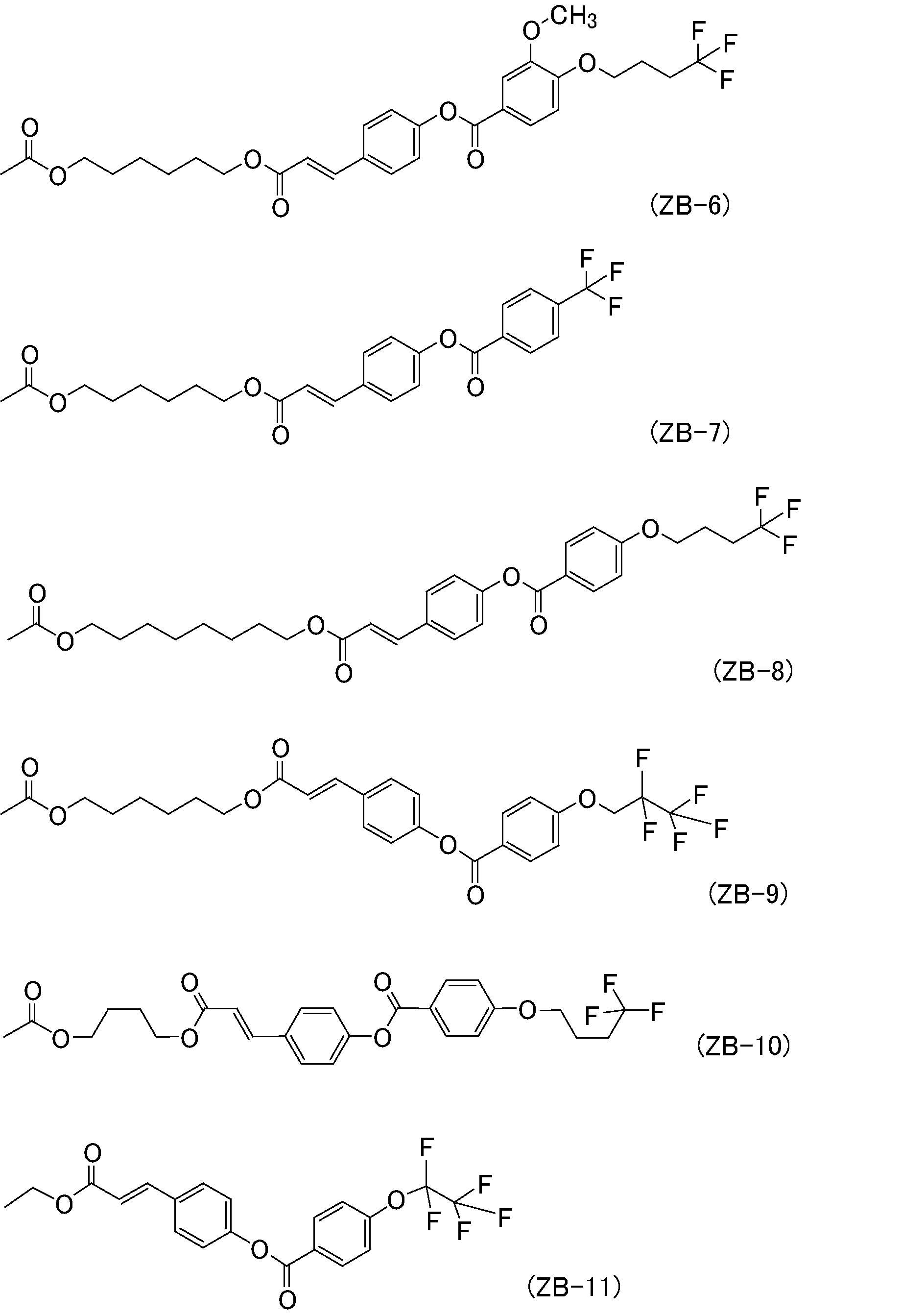
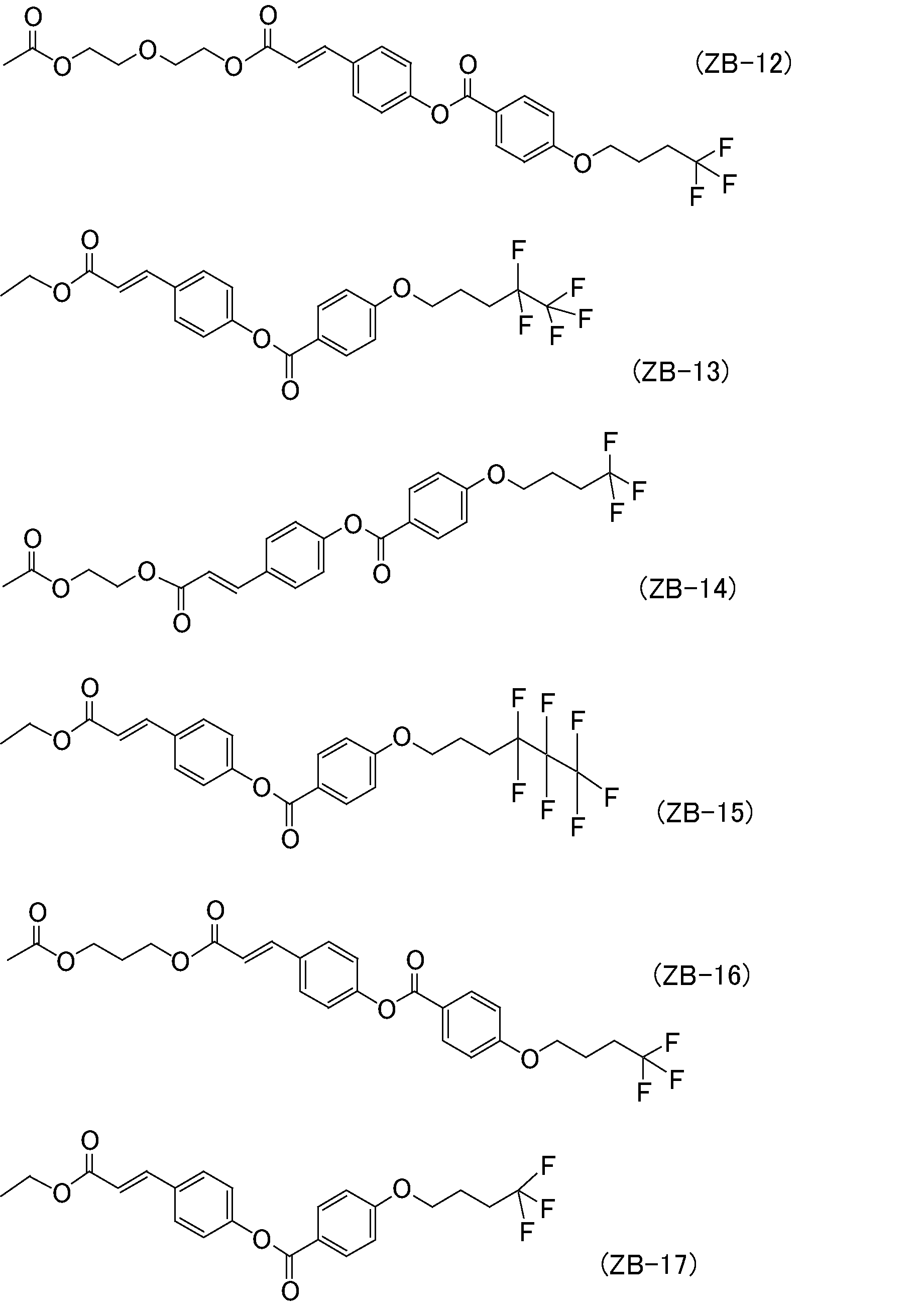

垂直配向膜11の膜厚は特に限定されず、適宜設定可能であるが、好ましくは20nm以上、500nm以下であり、より好ましくは50nm以上、200nm以下である。垂直配向膜11の膜厚が20nm未満の場合、基板全面に配向膜を均一に成膜できなくなる可能性がある。また、垂直配向膜11の膜厚が500nmを超えると配向膜の表面に凹凸が生じやすくなり、液晶化合物のチルト角がバラツキ、表示ムラを引き起こす可能性がある。
垂直配向膜11に含まれる垂直配向ポリマーの重量平均分子量は、10,000~1,000,000であることが好ましく、30,000~200,000であることがより好ましい。配向膜ポリマーの重量平均分子量を上記の範囲とすることにより、所望の膜厚で均一に成膜し易くなる。配向膜ポリマーの重量平均分子量が小さ過ぎると、所望の膜厚に成膜しにくく、膜厚が厚くなり過ぎると均一の膜厚にならず、配向膜の表面の凹凸が顕著になることがある。なお、本明細書において、重量平均分子量は、GPC(ゲルパーミエーションクロマトグラフィー)により測定することができる。
垂直配向ポリマーの主鎖は、ポリアミック酸、ポリイミド、ポリシロキサン又はポリビニルを有することが好ましい。
垂直配向ポリマーの主鎖がポリアミック酸構造を有する場合、下記化学式(P-1)で表される構造を有することが好ましく、垂直配向ポリマーの主鎖がポリイミド構造を有する場合、下記化学式(P-2)で表される構造を有することが好ましい。


上記化学式(P-1)及び(P-2)において、X1は4価の基を表し、環状構造を有する炭素数4~20の基であることが好ましく、炭素数6の芳香環基を1~3個又は炭素数4~6の脂環基を1~3個含む基であることがより好ましい。2個以上の芳香環基又は脂環基を含む場合は、それらが直接或いは連結基を介して結合していてもよいし、縮合していてもよい。連結基としては、炭素数1~5の炭化水素基、-O-、-N=N-、-C≡C-、-CH=CH-、-CO-CH=CH-等が挙げられる。
X1の具体例としては、下記化学式(X-1)~(X-16)で表される化学構造等が挙げられる。各構造に含まれる少なくとも一つの水素原子は、ハロゲン基、メチル基又はエチル基に置換されていてもよい。

上記化学式(P-1)及び(P-2)において、Y1は3価の基を表し、芳香環を有する炭素数6~20の基であることが好ましく、炭素数6の芳香環基を1~3個含む基であることがより好ましい。2個以上の芳香環基を含む場合は、それらが直接或いは連結基を介して結合していてもよいし、縮合していてもよい。連結基としては、炭素数1~5の炭化水素基、-O-、-N=N-、-C≡C-、-CH=CH-、-CO-CH=CH-等が挙げられる。
Y1の具体例としては、下記化学式(Y-1)~(Y-24)で表される化学構造等が挙げられる。各構造に含まれる少なくとも一つの水素原子は、ハロゲン基、メチル基又はエチル基に置換されていてもよい。

上記化学式(P-1)及び(P-2)におけるZ1は、末端に飽和脂肪族官能基を有する1価の基を表す。Z1は、-(RZ)d-(COO-Z)e、又は、-(RZ)d-(OCO-Z)eで表される基であることが好ましい。上記式中、RZは炭素数1~5のe+1価の基を表し、dは0又は1を表し、eは1又は2を表し、Zは環状構造を有し、かつ、末端に飽和脂肪族官能基を有する炭素数15~30の基を表す。
-(RZ)d-(COO-Z)e、又は、-(RZ)d-(OCO-Z)eで表される基の具体例としては、上記化学式(ZA-1)~(ZA-8)及び(ZB-1)~(ZB-21)で表される化学構造等が挙げられる。
上記化学式(P-1)及び(P-2)で表される構造の少なくとも一方を有する垂直配向ポリマーの重量平均分子量は、10,000~1,000,000であることが好ましく、30,000~200,000であることがより好ましい。配向膜ポリマーの重量平均分子量を上記の範囲とすることにより、所望の膜厚で均一に成膜し易くなる。配向膜ポリマーの重量平均分子量が小さ過ぎると、所望の膜厚に成膜しにくく、膜厚が厚くなり過ぎると均一の膜厚にならず、膜面の凹凸が顕著になることがある。
上記化学式(P-1)及び(P-2)で表される構造を有する垂直配向ポリマーの一分子において、X1、Y1及びZ1は、それぞれ、1種類であってもよく、2種類以上であってもよい。
垂直配向ポリマーの主鎖がポリシロキサン構造を有する場合、下記化学式(P-3)で表される構造を有することが好ましく、下記化学式(P-4)又は(P-5)で表される構造を有ることがより好ましい。


上記化学式(P-3)におけるX3は水素原子、ヒドロキシ基又は炭素数1~5のアルコキシ基を表す。炭素数1~5のアルコキシ基としては、-OCH3、-OC2H5、-OC3H7、-OC4H9、-OC5H11が挙げられ、直鎖構造であっても分岐構造であってもよい。上記化学式(P-3)におけるX3は水素原子、ヒドロキシ基、メトキシ基又はエトキシ基であることが好ましい。
上記化学式(P-3)~(P-5)におけるZ3は、末端に飽和脂肪族官能基を有する1価の基を表す。Z3は、好ましい範囲も含めて、上記化学式(P-1)及び(P-2)におけるZ1と同様である。
Z3の具体例としては、上記化学式(ZA-1)~(ZA-8)及び(ZB-1)~(ZB-21)で表される化学構造の他に、下記化学式(ZC-1)及び(ZC-2)で表される化学構造等が挙げられる。

上記化学式(P-3)~(P-5)で表される群より選択される少なくとも一種の構造を有する垂直配向ポリマーの重量平均分子量は、10,000~1,000,000であることが好ましく、30,000~200,000であることがより好ましい。配向膜ポリマーの重量平均分子量を上記の範囲とすることにより、所望の膜厚で均一に成膜し易くなる。配向膜ポリマーの重量平均分子量が小さ過ぎると、所望の膜厚に成膜しにくく、膜厚が厚くなり過ぎると均一の膜厚にならず、膜面の凹凸が顕著になることがある。
上記化学式(P-4)及び(P-5)におけるmは0<m<1の実数を表し、0.05<m<0.7であることが好ましく、0.2<m<0.5であることがより好ましい。
上記化学式(P-3)で表される構造を有する垂直配向ポリマーの一分子において、X3及びZ3は、それぞれ、1種類であってもよく、2種類以上であってもよい。また、上記化学式(P-4)及び(P-5)で表される構造を有する垂直配向ポリマーの一分子において、Z3は、1種類であってもよく、2種類以上であってもよい。
上記化学式(P-3)、(P-4)及び(P-5)で表される構造を有する垂直配向ポリマーの側鎖の末端Z3は、1種類であってもよく、2種類以上であってもよい。
垂直配向ポリマーの主鎖がポリビニル構造を有する場合、下記化学式(P-6)で表される構造を有することが好ましい。

上記化学式(P-6)におけるY6は水素原子又は炭素数1~5のアルキル基を表す。炭素数1~5のアルキル基としては、-CH3、-C2H5、-C3H7、-C4H9、-C5H11が挙げられ、直鎖構造であっても分岐構造であってもよい。上記化学式(P-6)におけるY6は水素原子、メチル基又はエチル基であることが好ましい。
上記化学式(P-6)におけるZ6は末端に飽和脂肪族官能基を有する1価の基を表す。Z6は、好ましい範囲も含めて、上記化学式(P-1)及び(P-2)におけるZ1と同様である。
Z6の具体例としては、上記化学式(ZA-1)~(ZA-8)、(ZB-1)~(ZB-21)、(ZC-1)及び(ZC-2)で表される化学構造等が挙げられる。
上記化学式(P-6)で表される構造を有する垂直配向ポリマーの重量平均分子量は、10,000~1,000,000であることが好ましく、30,000~200,000であることがより好ましい。配向膜ポリマーの重量平均分子量を上記の範囲とすることにより、所望の膜厚で均一に成膜し易くなる。配向膜ポリマーの重量平均分子量が小さ過ぎると、所望の膜厚に成膜しにくく、膜厚が厚くなり過ぎると均一の膜厚にならず、膜面の凹凸が顕著になることがある。
上記化学式(P-6)で表される構造を有する垂直配向ポリマーの一分子において、Y6及びZ6は、それぞれ、1種類であってもよく、2種類以上であってもよい。
垂直配向膜には、上記化学式(P-1)~(P-6)で表される少なくとも1種類の垂直配向ポリマーが含まれることが好ましく、2種類以上の垂直配向ポリマーが含まれていてもよい。垂直配向膜には上記化学式(P-1)又は(P-2)で表される垂直配向ポリマーが含まれることがより好ましく、上記化学式(P-1)又は(P-2)におけるX1は上記化学式(X-1)~(X-16)のいずれかで表される構造を表し、Y1は上記化学式(Y-1)~(Y-24)のいずれかで表される構造を表し、Z1は上記化学式(ZA-1)~(ZA-8)及び(ZB-1)~(ZB-21)のいずれかで表される構造であることが更に好ましい。
液晶パネル1の駆動方法としては、パッシブ駆動及びアクティブ駆動が挙げられる。パッシブ駆動は、上下の基板にストライプ状の電極を互いに交差するように配置し、交差しているそれぞれの電極を選択して電圧を加える駆動方法である。アクティブ駆動は、画素1つひとつにトランジスタ等のアクティブ素子を設け、このアクティブ素子のオン・オフにより駆動電圧の画素部への書き込みを可能にする駆動方法であり、画素部は、アクティブ素子がオフになった後にも蓄積容量によりこの電圧を保持する。
液晶パネル1はパッシブ駆動であることが好ましい。液晶パネル1をパッシブ駆動とすることで、トラン系液晶化合物を用いることにより発生するラジカルやイオンに由来するVHR〔Voltage Holding Ratio:電圧保持率〕低下を抑制することが可能となる。
液晶パネル1の液晶配向モードとしては、例えばVA-ECB(Vertical Alignment-Electrically Controlled Birefringence)モード等が挙げられる。
VA-ECBモードは、液晶分子の複屈折性を利用する液晶配向モード(以下、複屈折モードとも言う。)である。複屈折モードは、液晶分子への印加電圧を変化させることによって、位相差を変化させるモードである。複屈折モードの液晶パネルによれば、背面側偏光板を透過した直線偏光は、液晶パネルの複屈折性によってその偏光状態が変化し、通常は、付与される位相差の大きさに応じた楕円率を有する楕円偏光に変換される。よって、このように変換された楕円偏光が前面側偏光板を透過する量は、その楕円率(すなわち、印加電圧)によって変化することになる。
VA-ECBモードの液晶パネルにおいて、電圧無印加時に、液晶分子は各基板面に対して垂直配向するため、位相差はゼロである。VA-ECBモードの液晶パネルによれば、電圧無印加時に、背面側偏光板の透過軸と、前面側偏光板の透過軸とを平行にすると、両透過軸に平行な方向の直線偏光は、その偏光状態が変化することなく透過する。よって、VA-ECBモードの液晶パネルにおいては、電圧無印加時に、その透過光の色が無彩色となる。
一方、電圧を印加していくと、液晶分子は各基板面に対して平行な方向に徐々に倒れ、それに伴って位相差が徐々に増加する。その結果、液晶パネルの透過率が徐々に低下し、例えば、位相差が275nmであるときに波長550nmの光の透過率が最小となる。これは、透過軸が互いに平行な2枚の偏光板の間に位相差Rの媒質が配置される構成に対して、波長λの光を入射させる場合、その透過率は[cos(π×R/λ)]2に比例するためであり、例えば、位相差Rが波長λの半分のときに透過率が最小となる。ちなみに、波長550nmの光は、人間の視感度が最も高い波長の光である。
上述したような複屈折性による効果、すなわち、入射する偏光の偏光状態を変化させる効果、及び、その透過率を変化させる効果は、波長分散が大きい。そのため、複屈折モードの液晶パネルにおいては、通常、位相差がゼロである状態を除いて、その透過光の色が無彩色にならない。すなわち、複屈折モードの液晶パネルは、入射する偏光を透過させるときに、その偏光の偏光状態を変化させない非着色モード(位相差がゼロである状態)と、その偏光の偏光状態を変化させる着色モード(位相差がゼロではない状態)とに切り換え可能である。非着色モードは、例えば、VA-ECBモードの液晶パネルにおいては、電圧無印加時(複屈折性が発現しないように、閾値よりも大きな電圧を印加していない状態)に相当する。着色モードは、例えば、VA-ECBモードの液晶パネルにおいては、電圧印加時(複屈折性が発現するように、閾値よりも大きな電圧を印加した状態)に相当する。
[実施形態2]
<スイッチャブル・ミラーパネル>
実施形態2のスイッチャブル・ミラーパネルは、上記実施形態1の液晶パネル1に偏光板を設けた点以外は、実施形態1の液晶パネル1と同様の構成を有する。そこで、本実施形態では、本実施形態に特有の特徴について主に説明し、実施形態1と重複する内容については適宜説明を省略する。
<スイッチャブル・ミラーパネル>
実施形態2のスイッチャブル・ミラーパネルは、上記実施形態1の液晶パネル1に偏光板を設けた点以外は、実施形態1の液晶パネル1と同様の構成を有する。そこで、本実施形態では、本実施形態に特有の特徴について主に説明し、実施形態1と重複する内容については適宜説明を省略する。
図2は、実施形態2のスイッチャブル・ミラーパネルの断面模式図である。図2に示すように、本実施形態のスイッチャブル・ミラーパネル2は、背面側から前面側に向かって順に、反射型偏光板40と、液晶パネル1と、吸収型偏光板50とを備えている。反射型偏光板40は、液晶パネル1の背面側に、粘着剤等を介して貼り付けられていてもよい。吸収型偏光板50は、液晶パネル1の前面側に、粘着剤等を介して貼り付けられていてもよい。本明細書中、「背面側」は、例えば、図2中では、スイッチャブル・ミラーパネル2の下側(反射型偏光板40側)を指す。「前面側」は、例えば、図2中では、スイッチャブル・ミラーパネル2の上側(吸収型偏光板50側)を指す。本実施形態において、スイッチャブル・ミラーパネル2は前面側(吸収型偏光板50側)から観察される。
反射型偏光板40の透過軸と吸収型偏光板50の透過軸との関係は、液晶パネル1の液晶配向モードに合わせて適宜設定することができる。透明モードの透明性(背景の視認性)とミラーモードの鏡面性(鏡像の視認性)とを良好にする観点からは、反射型偏光板40の透過軸と吸収型偏光板50の透過軸とは、平行である又は直交することが好ましい。本明細書中、「2つの透過軸が平行である」とは、両者のなす角度が0±3°の範囲内であることを指し、好ましくは0±1°の範囲内であり、より好ましくは0±0.5°の範囲内であり、特に好ましくは0°(完全に平行)である。2つの透過軸が直交するとは、両者のなす角度が90±3°の範囲内であることを指し、好ましくは90±1°の範囲内であり、より好ましくは90±0.5°の範囲内であり、特に好ましくは90°(完全に直交)である。
反射型偏光板40としては、例えば、多層型反射型偏光板、ナノワイヤーグリッド偏光板、コレステリック液晶の選択反射を用いる反射型偏光板等を用いることができる。多層型反射型偏光板としては、例えば、スリーエム社製の反射型偏光板(製品名:DBEF)等が挙げられる。コレステリック液晶の選択反射を用いる反射型偏光板としては、例えば、日東電工社製の反射型偏光板(製品名:PCF)等が挙げられる。反射型偏光板2の反射率及び透過率は特に限定されず、2枚以上の反射型偏光板を互いの透過軸をずらして積層することによって、任意に調整可能である。本明細書中、「反射率」は、特に断りがない限り、視感反射率を指す。
吸収型偏光板50としては、例えば、ポリビニルアルコール(PVA)フィルムに二色性を有するヨウ素錯体等の異方性材料を吸着配向させたもの等を用いることができる。吸収型偏光板は、入射光のうちの吸収軸と平行な方向の偏光を吸収し、その吸収軸と直交する透過軸と平行な方向の偏光を透過させる機能を有するものである。
スイッチャブル・ミラーパネル2の役割は透明モードとミラーモードとの切り換えであるため、第一基板10、及び、第二基板20にカラーフィルタ層を配置しなくてもよい。
スイッチャブル・ミラーパネル2は、以下の原理で、透明モードとミラーモードとに切り換え可能である。すなわち、スイッチャブル・ミラーパネル2は、シースルーディスプレイとして使用可能である。ここで、透明モードは、液晶パネル1に印加された電圧により液晶層30中の液晶分子の配向が制御されることによって、反射型偏光板40の背面側からの入射光が吸収型偏光板50を透過する状態である。ミラーモードは、液晶パネル1に印加された電圧により液晶層30中の液晶分子の配向が制御されることによって、吸収型偏光板50の前面側からの入射光が反射型偏光板40で反射される状態である。以下では、液晶パネル1がVA-ECBモードの液晶パネルである場合について説明する。
まず、スイッチャブル・ミラーパネル2において、反射型偏光板40の透過軸と吸収型偏光板50の透過軸とが平行である場合について説明する。
(透明モード)
透明モードは、液晶パネル1の電圧無印加時に実現される。具体的には、以下の通りである。
透明モードは、液晶パネル1の電圧無印加時に実現される。具体的には、以下の通りである。
まず、反射型偏光板40の背面側からの入射光のうち、反射型偏光板40の透過軸と平行な方向に振動する成分は、反射型偏光板40を透過することで直線偏光となる。ここで、液晶パネル1の位相差はゼロであるため、反射型偏光板40を透過した直線偏光は、その偏光状態が変化することなく(非着色モード)、液晶パネル1(電圧無印加時)を透過する。そして、液晶パネル1を透過した直線偏光は、透過軸が反射型偏光板40の透過軸と平行である吸収型偏光板50を透過する。
一方、反射型偏光板40の背面側からの入射光のうち、反射型偏光板40の透過軸と直交する(反射軸と平行な)方向に振動する成分は、反射型偏光板40で背面側に反射される。
以上より、透明モードにおいて、スイッチャブル・ミラーパネル2の背面側が視認可能である。また、吸収型偏光板50の前面側からの入射光のうち、吸収型偏光板50の透過軸と平行な方向に振動する成分は、吸収型偏光板50、及び、液晶パネル1(電圧無印加時)を経て反射型偏光板40を透過し、吸収型偏光板50の透過軸と直交する(吸収軸と平行な)方向に振動する成分は、吸収型偏光板50で吸収される。よって、反射型偏光板40による外光(吸収型偏光板50の前面側からの入射光)の反射がないため、スイッチャブル・ミラーパネル2の背面側の視認性が低下することもない。
(ミラーモード)
ミラーモードは、液晶パネル1の電圧印加時に実現される。具体的には、以下の通りである。
ミラーモードは、液晶パネル1の電圧印加時に実現される。具体的には、以下の通りである。
まず、吸収型偏光板50の前面側からの入射光のうち、吸収型偏光板50の透過軸と平行な方向に振動する成分は、吸収型偏光板50を透過することで直線偏光となる。吸収型偏光板50を透過した直線偏光は、液晶パネル1(電圧印加時)を透過する際に、液晶パネル1の複屈折性によってその偏光状態が変化し(着色モード)、楕円偏光に変換される。そして、液晶パネル1を透過した楕円偏光のうち、反射型偏光板40の透過軸と平行な方向に振動する成分は、反射型偏光板40を透過する。これに対して、液晶パネル1を透過した楕円偏光のうち、反射型偏光板40の透過軸と直交する(反射軸と平行な)方向に振動する成分は、反射型偏光板40で直線偏光として反射される。そして、反射型偏光板40で反射された直線偏光は、液晶パネル1を透過する際に、液晶パネル1の複屈折性によってその偏光状態が変化し、楕円偏光に変換される。その後、液晶パネル1を透過した楕円偏光のうち、吸収型偏光板50の透過軸と平行な方向に振動する成分は、吸収型偏光板50を透過し、前面側に反射光として出射される。液晶パネル1を透過した楕円偏光のうち、吸収型偏光板50の透過軸と直交する(吸収軸と平行な)方向に振動する成分は、吸収型偏光板50で吸収される。
一方、吸収型偏光板50の前面側からの入射光のうち、吸収型偏光板50の透過軸と直交する(吸収軸と平行な)方向に振動する成分は、吸収型偏光板50で吸収される。
以上より、ミラーモードにおいて、反射光による鏡像が視認可能である。更に、液晶パネル1はセグメント電極を有しているため、一部の画素に電圧を印加することによって、反射光による文字、画像等の情報が表示可能である。この場合、複屈折性による偏光状態の変化、並びに、それに伴う透過率及び反射率の変化は波長分散が大きいため、反射光の強度は波長によって異なることになる。すなわち、ミラーモードにおいて、反射光が色づいて見える。一方、電圧が印加されていない画素では、スイッチャブル・ミラーパネル2の背面側が視認可能である。
液晶パネル1が複屈折モード(例えば、VA-ECBモード)の液晶パネルである場合、反射光の色は、液晶パネル1が付与する実効的な位相差によって調整可能である。本明細書中、「実効的な位相差」(単に、位相差とも言う。)は、複屈折モードの液晶パネルに対してある大きさの電圧を印加した状態で、その法線方向から観測される位相差のことを指す。例えば、VA-ECBモードの液晶パネルにおいて、電圧無印加時に、液晶分子は各基板面に対して垂直配向するため、実効的な位相差はゼロである。一方、電圧を印加していくと、液晶分子は各基板面に対して平行な方向に徐々に倒れ、それに伴って実効的な位相差が徐々に増加する。そして、すべての液晶分子が各基板面に対して平行な方向に一様に倒れたときに、実効的な位相差が最大となる。ここで、液晶パネル1を構成する液晶(液晶層30)の屈折率異方性をΔn、厚みをdとすると、実効的な位相差の最大値は、原理的に、Δnd(以下、液晶リタデーションとも言う。)となる。
実際の液晶パネル1の構成及び材料では、すべての液晶分子が一様に配向することは難しく、一般的には、液晶層30の厚み方向及び水平方向の少なくとも一方に対して一様に分布しない。例えば、基板近傍に存在する液晶分子は、配向膜の配向規制力のために、電圧印加時にも動きにくい。これに対して、厚み方向の中心部付近に存在する液晶分子は、電圧印加時に動きやすいため、液晶分子の配向状態は厚み方向に対して一様ではない。このような理由により、実効的な位相差の最大値は、実際は、液晶リタデーション(Δnd)と完全に一致せず、液晶リタデーションよりもやや小さくなる。しかしながら、液晶リタデーションが大きいほど、実効的な位相差の最大値が大きくなり、複屈折モードの液晶パネル1で実現可能な位相差の範囲が広がることには違いない。そのため、反射光の色を調整するためには、複屈折モードの液晶パネル1の液晶リタデーションをどのような値に設定するかが重要であり、液晶リタデーションが大きいほど好ましい。
上述したように、複屈折モードの液晶パネル1の透過率は、原理的に、実効的な位相差が入射光の波長の半分のときに最小となる。すなわち、実効的な位相差を、入射光の波長の半分よりも大きな値まで変化させることは、液晶分子の配向状態を充分に変化させる、例えば、VA-ECBモードの液晶パネルの場合、液晶分子が各基板面に対して垂直配向した状態から水平配向した状態へ変化させることに相当する。よって、着色モードにおいて、複屈折モードの液晶パネル1が、入射光の波長の半分よりも大きな位相差(実効値)を付与すれば、反射光の色を調整することができる。このような複屈折モードの液晶パネル1の位相差は、通常、人間の視感度が最も高い波長550nmの光に対して設計される。そのため、着色モードにおいて、複屈折モードの液晶パネル1は、波長550nmの光で測定したときに275nmよりも大きな値まで位相差を変化させ得ることが好ましい。これにより、反射光の色を調整することができる。
次に、スイッチングミラーパネル2において、反射型偏光板40の透過軸と吸収型偏光板50の透過軸とが直交する場合について説明する。
(透明モード)
透明モードは、液晶パネル1の電圧印加時に実現される。具体的には、以下の通りである。
透明モードは、液晶パネル1の電圧印加時に実現される。具体的には、以下の通りである。
まず、反射型偏光板40の背面側からの入射光のうち、反射型偏光板40の透過軸と平行な方向に振動する成分は、反射型偏光板40を透過することで直線偏光となる。反射型偏光板40を透過した直線偏光は、液晶パネル1(電圧印加時)を透過する際に、液晶パネル1の複屈折性によってその偏光状態が変化し(着色モード)、楕円偏光に変換される。そして、液晶パネル1を透過した楕円偏光のうち、吸収型偏光板50の透過軸と平行な方向に振動する成分は、吸収型偏光板50を透過する。これに対して、液晶パネル1を透過した楕円偏光のうち、吸収型偏光板50の透過軸と直交する(吸収軸と平行な)方向に振動する成分は、吸収型偏光板50で吸収される。
一方、反射型偏光板40の背面側からの入射光のうち、反射型偏光板40の透過軸と直交する(反射軸と平行な)方向に振動する成分は、反射型偏光板40で背面側に反射される。
以上より、透明モードにおいて、スイッチャブル・ミラーパネル2の背面側が視認可能である。この場合、複屈折性による偏光状態の変化、及び、それに伴う透過率の変化は波長分散が大きいため、背面側からスイッチャブル・ミラーパネル2を透過する透過光の強度は波長によって異なることになる。すなわち、透明モードにおいて、透過光が色づいて見える。
(ミラーモード)
ミラーモードは、液晶パネル1の電圧無印加時に実現される。具体的には、以下の通りである。
ミラーモードは、液晶パネル1の電圧無印加時に実現される。具体的には、以下の通りである。
まず、吸収型偏光板50の前面側からの入射光のうち、吸収型偏光板50の透過軸と平行な方向に振動する成分は、吸収型偏光板50を透過することで直線偏光となる。ここで、液晶パネル1の位相差はゼロであるため、吸収型偏光板50を透過した直線偏光は、その偏光状態が変化することなく(非着色モード)、液晶パネル1(電圧無印加時)を透過する。そして、液晶パネル1を透過した直線偏光は、反射軸が吸収型偏光板50の透過軸と平行である反射型偏光板40で反射される。その後、反射型偏光板40で反射された直線偏光は、液晶パネル1、及び、吸収型偏光板50を順に透過し、前面側に反射光として出射される。
一方、吸収型偏光板50の前面側からの入射光のうち、吸収型偏光板50の透過軸と直交する(吸収軸と平行な)方向に振動する成分は、吸収型偏光板50で吸収される。
以上より、ミラーモードにおいて、反射光による鏡像が視認可能である。更に、液晶パネル1はセグメント電極を有しているため、一部の画素を電圧無印加状態にすることによって、反射光による文字、画像等の情報が表示可能である。この場合、反射光は色づいて見えない(無彩色である)。一方、電圧が印加されている画素では、スイッチャブル・ミラーパネル2の背面側が視認可能である。
液晶パネル1が複屈折モード(例えば、VA-ECBモード)の液晶パネルである場合、透明モードにおけるスイッチャブル・ミラーパネル2の透過率を高める観点からは、反射型偏光板40の透過軸と吸収型偏光板50の透過軸とは平行であることが好ましい。これは、反射型偏光板40の透過軸と吸収型偏光板50の透過軸とが直交する場合、上述したように、透明モードは液晶パネル1の電圧印加時に実現され、位相差が存在するためである。
[実施形態3]
<スイッチャブル・ミラーディスプレイ>
実施形態3のスイッチャブル・ミラーディスプレイは、上記実施形態2のスイッチャブル・ミラーパネル2に加えて、表示装置を設けた点以外は、実施形態2のスイッチャブル・ミラーパネル2と同様の構成を有する。そこで、本実施形態では、本実施形態に特有の特徴について主に説明し、実施形態2と重複する内容については適宜説明を省略する。
<スイッチャブル・ミラーディスプレイ>
実施形態3のスイッチャブル・ミラーディスプレイは、上記実施形態2のスイッチャブル・ミラーパネル2に加えて、表示装置を設けた点以外は、実施形態2のスイッチャブル・ミラーパネル2と同様の構成を有する。そこで、本実施形態では、本実施形態に特有の特徴について主に説明し、実施形態2と重複する内容については適宜説明を省略する。
図3は、実施形態3のスイッチャブル・ミラーディスプレイの断面模式図である。実施形態3のスイッチャブル・ミラーディスプレイ3は、背面側から前面側に向かって順に、バックライト60と、液晶表示部2aと、スイッチャブル・ミラーパネル2とを備えている。
本実施形態では、スイッチャブル・ミラーパネル2と液晶表示部2aとが離間して(空気層を介して)配置される構成を示したが、両者が粘着剤等を介して貼り合わされる構成であってもよい。
液晶表示部2aは、背面側から前面側に向かって順に、吸収型偏光板50aと、表示用液晶パネル1aと、吸収型偏光板50bとを有している。吸収型偏光板50aは、表示用液晶パネル1aの背面側に、粘着剤等を介して貼り付けられていてもよい。吸収型偏光板50bは、表示用液晶パネル1aの前面側に、粘着剤等を介して貼り付けられていてもよい。本実施形態において、スイッチャブル・ミラーディスプレイ3は、前面側(吸収型偏光板50b側)から観察される。すなわち、スイッチャブル・ミラーディスプレイ3の表示面は、スイッチャブル・ミラーパネル2側である。
吸収型偏光板50aの透過軸と吸収型偏光板50bの透過軸との関係は、表示用液晶パネル1aの液晶配向モードに合わせて適宜設定することができる。なお、吸収型偏光板50bを省略し、その機能を反射型偏光板40に代替させてもよい。ただし、一般的に、反射型偏光板の偏光度は、吸収型偏光板の偏光度と比較して低いため、吸収型偏光板50bを省略すると、ディスプレイモードにおけるコントラストが低下する。逆に言えば、反射型偏光板40の偏光度が充分であれば、吸収型偏光板50bを省略することができる。吸収型偏光板50bを省略するためには、反射型偏光板40の偏光度は90%以上(コントラスト比が10以上)であることが好ましく、99%以上(コントラスト比が100以上)であることがより好ましい。
吸収型偏光板50a、及び、吸収型偏光板50bとしては、例えば、ポリビニルアルコールフィルムに二色性を有するヨウ素錯体等の異方性材料を吸着配向させたもの等を用いることができる。
バックライト60の方式は特に限定されず、例えば、エッジライト方式、直下型方式等が挙げられる。バックライト60の光源の種類は特に限定されず、例えば、発光ダイオード(LED)、冷陰極管(CCFL)等が挙げられる。
表示用液晶パネル1aは、一対の基板10a、20a間に液晶層30aを挟持する構成を有しており、基板10aと液晶層30aの間、及び、基板20aと液晶層との間には、配向膜11aが設けられている。また、表示用液晶パネル1aを構成する一対の基板10a、20aは、液晶層30aを挟持するように、シール材を介して貼り合わされている。
表示用液晶パネル1aを構成する一対の基板10a、20aの種類は特に限定されず、例えば、アクティブ基板10bとカラーフィルタ基板20bとの組み合わせ等が挙げられる。
アクティブ基板10bとしては、例えば、ガラス基板、プラスチック基板等の透明基板上に、薄膜トランジスタ素子等の各種配線が配置される構成であってもよい。薄膜トランジスタ素子が有する半導体層の構成は特に限定されず、例えば、アモルファスシリコン、低温ポリシリコン、酸化物半導体等を含むものであってもよい。酸化物半導体の構成としては、例えば、インジウム、ガリウム、亜鉛、及び、酸素から構成される化合物、インジウム、亜鉛、及び、酸素から構成される化合物等が挙げられる。酸化物半導体として、インジウム、ガリウム、亜鉛、及び、酸素から構成される化合物を用いる場合は、オフリーク電流が少ないため、一旦電圧を印加すると、次のデータ信号(電圧)を書き込む(印加する)まで電圧印加状態を保持する休止駆動が可能となる。よって、低消費電力の観点からは、酸化物半導体として、インジウム、ガリウム、亜鉛、及び、酸素から構成される化合物を用いることが好ましい。
カラーフィルタ基板20bとしては、例えば、ガラス基板、プラスチック基板等の透明基板上に、カラーフィルタ層等が配置される構成であってもよい。カラーフィルタ層の色の組み合わせは特に限定されず、例えば、赤色、緑色、及び、青色の組み合わせ、赤色、緑色、青色、及び、黄色の組み合わせ等が挙げられる。
表示用液晶パネル1aの液晶配向モードは特に限定されず、例えば、MVA(Multi-domain Vertical Alignment)モード、FFS(Fringe Field Switching)モード、VA(Vertical Alignment)モード、IPS(In-Plane Switching)モード、OCB(Optically Compensated Birefringence)モード、TNモード等が挙げられ、FFSモードであることが好ましい。
MVAモードの液晶パネルは、電圧無印加時に、負の誘電率異方性を有する液晶分子を各基板面に対して垂直配向させるものである。MVAモードの液晶パネルによれば、少なくとも一方の基板に配置されるリブ、スリット等の構造体によって、電圧印加時に、液晶分子の倒れる方向が複数の方向に制御されるため、広視野角を実現することができる。また、光配向膜の配向分割を利用したUV2A(Ultra-violet induced multi-domain Vertical Alignment)モードも、MVAモードの一種である。
FFSモードの液晶パネルにおいて、一対の基板上に配置される配向膜には、互いに反平行(アンチパラレル)方向にラビング処理が施されているため、電圧無印加時に、液晶分子は各基板面に対して水平配向する。ここで、FFSモードの液晶パネルを構成する一対の基板のうちの一方には、液晶層側から順に、スリット状の上層電極(櫛歯電極)と、透明絶縁膜(例えば、窒化膜)と、平面状(ベタ状)の下層電極とが配置されている。このような構成によれば、上層電極と下層電極との間に電圧を印加することによって、フリンジ電界が発生する。よって、FFSモードの液晶パネルによれば、フリンジ電界によって液晶分子の配向方向を変化させることができ、その結果、透過光量が変化する。
本実施形態では、スイッチャブル・ミラーパネル2の背面側に、液晶表示部2aが配置される構成を示したが、液晶表示部2aの代わりに、偏光板を有する他の表示装置が配置されていてもよい。他の表示装置としては、例えば、反射防止用の吸収型円偏光板が設けられた有機エレクトロルミネッセンス表示装置、偏光板が貼り付けられたMEMS(Micro Electro Mechanical Systems)ディスプレイ等の、偏光を出射する表示装置が挙げられる。
スイッチャブル・ミラーディスプレイ3は、以下の原理で動作させることができる。ここでは、液晶パネル1がVA-ECBモードの液晶パネル、表示用液晶パネル1aがMVAモード又はFFSモードの液晶パネルである場合について説明する。
まず、スイッチャブル・ミラーパネル2において、反射型偏光板40の透過軸と吸収型偏光板50の透過軸とが平行である場合について説明する。液晶表示部2aにおいて、吸収型偏光板50aの透過軸と吸収型偏光板50bの透過軸とは直交する。反射型偏光板40の透過軸と吸収型偏光板50bの透過軸とは平行である。
(透明モード)
透明モードは、液晶パネル1の電圧無印加時に実現される。具体的には、以下の通りである。
透明モードは、液晶パネル1の電圧無印加時に実現される。具体的には、以下の通りである。
表示用液晶パネル1aが画像を表示する場合(ディスプレイモード)、液晶表示部2aから出射される直線偏光(吸収型偏光板50bを透過した直線偏光)は、透過軸が吸収型偏光板50bの透過軸と平行である反射型偏光板40を透過する。ここで、液晶パネル1の位相差はゼロであるため、反射型偏光板40を透過した直線偏光は、その偏光状態が変化することなく(非着色モード)、液晶パネル1(電圧無印加時)を透過する。そして、液晶パネル1を透過した直線偏光は、透過軸が反射型偏光板40の透過軸と平行である吸収型偏光板50を透過する。すなわち、スイッチャブル・ミラーパネル2が配置されているにも関わらず、それが無い場合と同様に表示用液晶パネル1aの画像が視認可能である。
一方、吸収型偏光板50の前面側からの入射光のうち、吸収型偏光板50の透過軸と平行な方向に振動する成分は、吸収型偏光板50を透過することで直線偏光となる。吸収型偏光板50を透過した直線偏光は、その偏光状態が変化することなく、液晶パネル1を透過する。そして、液晶パネル1を透過した直線偏光は、透過軸が吸収型偏光板50の透過軸と平行である反射型偏光板40を透過する。その後、反射型偏光板40を透過した直線偏光は吸収型偏光板50bを透過するが、吸収型偏光板50a、又は、表示用液晶パネル1aが有するカラーフィルタ層、ブラックマトリクス等で吸収される。そのため、スイッチャブル・ミラーディスプレイ3の前面側に反射光として戻る成分はほとんどない。
以上より、透明モードにおいて、表示用液晶パネル1aの画像が視認可能である。また、反射型偏光板40による外光(吸収型偏光板50の前面側からの入射光)の反射がないため、表示用液晶パネル1aの画像の視認性が低下することもない。なお、透明モードにおいて、表示用液晶パネル1aは非表示状態であってもよい。
(ミラーモード)
ミラーモードは、液晶パネル1の電圧印加時に実現される。具体的には、以下の通りである。
ミラーモードは、液晶パネル1の電圧印加時に実現される。具体的には、以下の通りである。
表示用液晶パネル1aは非表示状態である。この場合、表示用液晶パネル1aは、その全体又は一部で表示を行わないことが好ましい。表示を行わない形態としては、黒表示を行ったり、バックライト60を消灯又は減光したりして、液晶表示部2aから表示光を出射しない形態も含まれる。
一方、吸収型偏光板50の前面側からの入射光のうち、吸収型偏光板50の透過軸と平行な方向に振動する成分は、吸収型偏光板50を透過することで直線偏光となる。吸収型偏光板50を透過した直線偏光は、液晶パネル1(電圧印加時)を透過する際に、液晶パネル1の複屈折性によってその偏光状態が変化し(着色モード)、楕円偏光に変換される。そして、液晶パネル1を透過した楕円偏光のうち、反射型偏光板40の透過軸と平行な方向に振動する成分は、反射型偏光板40を透過し、その後、吸収型偏光板50a、又は、表示用液晶パネル1aが有するカラーフィルタ層、ブラックマトリクス等で吸収される。これに対して、液晶パネル1を透過した楕円偏光のうち、反射型偏光板40の透過軸と直交する(反射軸と平行な)方向に振動する成分は、反射型偏光板40で直線偏光として反射される。そして、反射型偏光板40で反射された直線偏光は、液晶パネル1を透過する際に、液晶パネル1の複屈折性によってその偏光状態が変化し、楕円偏光に変換される。その後、液晶パネル1を透過した楕円偏光のうち、吸収型偏光板50の透過軸と平行な方向に振動する成分は、吸収型偏光板50を透過し、前面側に反射光として出射される。液晶パネル1を透過した楕円偏光のうち、吸収型偏光板50の透過軸と直交する(吸収軸と平行な)方向に振動する成分は、吸収型偏光板50で吸収される。
以上より、ミラーモードにおいて、反射光による鏡像が視認可能である。更に、液晶パネル1はセグメント電極を有しているため、一部の画素に電圧を印加することによって、反射光による文字、画像等の情報が表示可能である。この場合、複屈折性による偏光状態の変化、並びに、それに伴う透過率及び反射率の変化は波長分散が大きいため、反射光の強度は波長によって異なることになる。すなわち、ミラーモードにおいて、反射光が色づいて見える。一方、電圧が印加されていない画素では、表示用液晶パネル1aの画像が視認可能である。
次に、スイッチャブル・ミラーパネル2において、反射型偏光板40の透過軸と吸収型偏光板50の透過軸とが直交する場合について説明する。液晶表示部2aにおいて、吸収型偏光板50aの透過軸と吸収型偏光板50bの透過軸とは直交する。反射型偏光板40の透過軸と吸収型偏光板50bの透過軸とは平行である。
(透明モード)
透明モードは、液晶パネル1の電圧印加時に実現される。具体的には、以下の通りである。
透明モードは、液晶パネル1の電圧印加時に実現される。具体的には、以下の通りである。
表示用液晶パネル1aが画像を表示する場合(ディスプレイモード)、液晶表示部2aから出射される直線偏光(吸収型偏光板50bを透過した直線偏光)は、透過軸が吸収型偏光板50bの透過軸と平行である反射型偏光板40を透過する。反射型偏光板40を透過した直線偏光は、液晶パネル1(電圧印加時)を透過する際に、液晶パネル1の複屈折性によってその偏光状態が変化し(着色モード)、楕円偏光に変換される。そして、液晶パネル1を透過した楕円偏光のうち、吸収型偏光板50の透過軸と平行な方向に振動する成分は、吸収型偏光板50を透過する。これに対して、液晶パネル1を透過した楕円偏光のうち、吸収型偏光板50の透過軸と直交する(吸収軸と平行な)方向に振動する成分は、吸収型偏光板50で吸収される。以上より、スイッチャブル・ミラーパネル2が配置されているにも関わらず、それが無い場合と同様に表示用液晶パネル1aの画像が視認可能である。
以上より、透明モードにおいて、表示用液晶パネル1aの画像が視認可能である。この場合、複屈折性による偏光状態の変化、及び、それに伴う透過率の変化は波長分散が大きいため、液晶表示部2aから出射される表示光の強度は波長によって異なることになる。すなわち、透明モードにおいて、表示光が色づいて見える。なお、透明モードにおいて、表示用液晶パネル1aは非表示状態であってもよい。
(ミラーモード)
ミラーモードは、液晶パネル1の電圧無印加時に実現される。具体的には、以下の通りである。
ミラーモードは、液晶パネル1の電圧無印加時に実現される。具体的には、以下の通りである。
表示用液晶パネル1aは非表示状態である。この場合、表示用液晶パネル1aは、その全体又は一部で表示を行わないことが好ましい。表示を行わない形態としては、黒表示を行ったり、バックライト60を消灯又は減光したりして、液晶表示部2aから表示光を出射しない形態も含まれる。
吸収型偏光板50の前面側からの入射光のうち、吸収型偏光板50の透過軸と平行な方向に振動する成分は、吸収型偏光板50を透過することで直線偏光となる。ここで、液晶パネル1の位相差はゼロであるため、吸収型偏光板50を透過した直線偏光は、その偏光状態が変化することなく(非着色モード)、液晶パネル1(電圧無印加時)を透過する。そして、液晶パネル1を透過した直線偏光は、反射軸が吸収型偏光板50の透過軸と平行である反射型偏光板40で反射される。その後、反射型偏光板40で反射された直線偏光は、液晶パネル1、及び、吸収型偏光板50を順に透過し、前面側に反射光として出射される。
以上より、ミラーモードにおいて、反射光による鏡像が視認可能である。更に、液晶パネル1はセグメント電極を有しているため、一部の画素を電圧無印加状態にすることによって、反射光による文字、画像等の情報が表示可能である。この場合、反射光は色づいて見えない(無彩色である)。一方、電圧が印加されている画素では、表示用液晶パネル1aの画像が視認可能である。
液晶表示部2aとスイッチャブル・ミラーパネル2とは、粘着剤を介して貼り合わされていてもよい。粘着剤としては、例えば、光学透明粘着(OCA(Optical Clear Adhesive))シート等が挙げられる。
図4は、実施形態3のスイッチャブル・ミラーディスプレイの概念図である。スイッチャブル・ミラーディスプレイ3は、背面側から前面側に向かって順に、バックライト60と、液晶表示部2aと、スイッチャブル・ミラーパネル2とを備えており、液晶表示部2aは、背面側から前面側に向かって順に、吸収型偏光板50aと、表示用液晶パネル1aと、吸収型偏光板50bとを備えている。
スイッチャブル・ミラーパネル2の液晶層30に含まれるトラン系液晶化合物は、バックライト60からの紫外光等によりπ結合が開裂しラジカルやイオンを発生する。ここで、本実施形態のスイッチャブル・ミラーディスプレイ3は、スイッチャブル・ミラーパネル2とバックライト60との間に液晶表示部2aを有しており、さらに液晶表示部2aは2枚の吸収型偏光板50a、50bに挟持された表示用液晶パネル1aを有する構成である。液晶表示部2aにおける2枚の吸収型偏光板50a、50bは、380nmまでの紫外光を吸収するため、スイッチャブル・ミラーパネル2の液晶層30に含まれるトラン系液晶化合物に由来するラジカルやイオンの発生速度を遅くすることが可能となる。
以下に、実施例及び比較例を挙げて本発明をより詳細に説明するが、本発明はこれらの例によって限定されるものではない。
[実施例1]
実施例1では、上述した実施形態1の液晶パネル1を以下の方法で実際に作製した。
まず、パッシブ駆動型の液晶パネル1を作製するために、ストライプ状のITO電極を有する一対の基板10、20を用意し、下記化学式(P-1-1)に示す垂直配向ポリマーを含有する溶剤を、各基板10、20上に塗布し、90℃、5分の仮焼成を行い、続いて200℃、40分の本焼成を行った。焼成処理を行うことで、高分子主鎖がポリイミドであり、高分子側鎖の末端が飽和脂肪族官能基である下記化学式(P-1-1)に示す垂直配向ポリマーを含む垂直配向膜11(膜厚50~160nm)を形成した。
実施例1では、上述した実施形態1の液晶パネル1を以下の方法で実際に作製した。
まず、パッシブ駆動型の液晶パネル1を作製するために、ストライプ状のITO電極を有する一対の基板10、20を用意し、下記化学式(P-1-1)に示す垂直配向ポリマーを含有する溶剤を、各基板10、20上に塗布し、90℃、5分の仮焼成を行い、続いて200℃、40分の本焼成を行った。焼成処理を行うことで、高分子主鎖がポリイミドであり、高分子側鎖の末端が飽和脂肪族官能基である下記化学式(P-1-1)に示す垂直配向ポリマーを含む垂直配向膜11(膜厚50~160nm)を形成した。

続いて、各垂直配向膜11に、貼り合わせ後のラビング方向が互いに反平行方向になるようにラビング処理を施した。次に、一方の基板に、ディスペンサを使用して紫外線硬化性シール剤(積水化学工業社製、フォトレック(登録商標)S-WB)を描画した。また、もう一方の基板上の所定の位置に、上記化学式(T)で示したトラン系液晶化合物を含有するネガ型液晶材料(Tni(液晶材料のネマティック-アイソトロピック転移点)=90℃、Δn=0.19、Δε=-5)を滴下した。
続いて、真空下にて両基板10、20を貼り合わせ、シール剤を紫外光にて硬化させた。このようにして得られた液晶セルにおける液晶化合物の流動配向を消すために、液晶セルを130℃で40分間加熱し、液晶を等方相にする再配向処理を行い、その後室温まで冷却してVA-ECBモード液晶パネル1を得た。
[比較例1]
実施例1とは異なる配向膜材料を用いたこと以外は実施例1と同様にして、比較例1の液晶パネルを作製した。本比較例では、実施例1における上記化学式(P-1-1)に示す垂直配向ポリマーに代えて、下記化学式(PR-1-1)に示すポリマーを用い、下記化学式(PR-1-1)に示すポリマーを含む配向膜(膜厚50~160nm)を各基板上に形成した。
実施例1とは異なる配向膜材料を用いたこと以外は実施例1と同様にして、比較例1の液晶パネルを作製した。本比較例では、実施例1における上記化学式(P-1-1)に示す垂直配向ポリマーに代えて、下記化学式(PR-1-1)に示すポリマーを用い、下記化学式(PR-1-1)に示すポリマーを含む配向膜(膜厚50~160nm)を各基板上に形成した。

[実施例1及び比較例1のバックライト上放置試験]
まず、実施例1及び比較例1に係る液晶パネルをバックライト上に放置する前の初期の残留DCを、フリッカ消去法にて測定した。残留DCの測定条件は、2VのDCオフセットを70℃で2時間印加してから行った。また、不純物発生の指標とするため、実施例1及び比較例1に係る液晶パネルをバックライト上に放置する前の、初期のVHRを測定した。VHRの測定は、東陽テクニカ社製6254型VHR測定システムを用いて、1V、70℃の条件で行った。以上より、実施例1及び比較例1に係る液晶パネルをバックライト上に放置する前の、初期の残留DC及びVHRを測定した。なお、VHR及び残留DCの測定は、パッシブ駆動型の1画素テストセルを用いて行った。また、残留DCはrDCともいう。
まず、実施例1及び比較例1に係る液晶パネルをバックライト上に放置する前の初期の残留DCを、フリッカ消去法にて測定した。残留DCの測定条件は、2VのDCオフセットを70℃で2時間印加してから行った。また、不純物発生の指標とするため、実施例1及び比較例1に係る液晶パネルをバックライト上に放置する前の、初期のVHRを測定した。VHRの測定は、東陽テクニカ社製6254型VHR測定システムを用いて、1V、70℃の条件で行った。以上より、実施例1及び比較例1に係る液晶パネルをバックライト上に放置する前の、初期の残留DC及びVHRを測定した。なお、VHR及び残留DCの測定は、パッシブ駆動型の1画素テストセルを用いて行った。また、残留DCはrDCともいう。
続いて、実施例1及び比較例1に係る液晶パネルをバックライト上に放置した後、残留DC及びVHRを以下の方法により測定した。すなわち、実施例1及び比較例1にて作製した液晶パネルを、それぞれ、バックライト60上に下記の2つの条件で100時間放置した後、上記と同様に残留DC及びVHRを測定した。
<条件1>カラーフィルタ基板が設けられた表示用液晶パネルと一対の偏光板とを備えるFFSモードの液晶表示部をバックライト60上に置き、その上に実施例1又は比較例1で作製した液晶パネルを直接置く。なお、FFSモードの液晶表示部は、後述の実施例4で用いた液晶表示部2aと同様である。
<条件2>バックライト60上に、実施例1又は比較例1で作製した液晶パネルを直接置く。
<条件2>バックライト60上に、実施例1又は比較例1で作製した液晶パネルを直接置く。
実施例1及び比較例1のバックライト上放置試験の結果を下記表1に示す。

表1に示したように、垂直配向膜11に含まれる垂直配向ポリマーの側鎖が飽和脂肪族官能基である実施例1の液晶パネル1を用いた場合、初期の残留DCは条件1及び条件2共に20mVと小さかった。
また、液晶表示部2aを介してバックライト60上に実施例1の液晶パネル1を配置した条件1では、100時間放置後の残留DCは30mVであり、初期の残留DCからほとんど増加(悪化)しなかった。一方、液晶表示部2aを介さず、実施例1の液晶パネル1をバックライト60上に直接配置した条件2では、100時間放置後の残留DCは70mVまで増加した。また条件2ではVHRが96%台まで低下していることから、バックライト光によりトラン系液晶化合物のラジカル化やイオン化が進んだものと考えられる。
しかしながら、実施例1の液晶パネル1は、比較例1の液晶パネルと比べて残留DCは低い。これは、垂直配向膜11に含まれる垂直配向ポリマーの側鎖の末端を飽和脂肪族官能基とすることにより、初期及びバックライト上放置後のいずれにおいても、液晶層30に含まれるトラン系液晶化合物に由来するラジカルやイオンと垂直配向膜11とのπ-π相互作用が抑制されたためと考えられる。バックライト60上に100時間放置すること等により形成された、トラン系液晶化合物に由来するラジカルやイオンは、垂直配向膜11の表面にほとんど吸着していないことを示唆していると考えられる。 また、実施例1において、バックライト60上に100時間放置した後の残留DCは、条件1の方が条件2よりも低く抑えられたのは、条件1において、実施例1の液晶パネル1とバックライト60との間に液晶表示部2aを設けたため、バックライト60からの紫外光が液晶表示部2aに効果的に吸収され、実施例1の液晶パネル1においてトラン系液晶化合物のラジカル化やイオン化の速度が遅くなったためと考えられる。
垂直配向膜に含まれる垂直配向ポリマーの側鎖の末端が芳香族基である比較例1の液晶パネルを用いた場合、初期のVHRは実施例1とほとんど違いはないものの、残留DCは40mVとやや大きくなっている。さらに、液晶表示部2aを介してバックライト60上に比較例1の液晶パネルを配置した条件1では、100時間放置後の残留DCは120mVまで増加し、VHRは96.8%まで低下した。また、液晶表示部2aを介さず、比較例1の液晶パネルをバックライト60上に直接配置した条件2では、100時間放置後の残留DCは180mVまで増加し、VHRは94.5%まで低下した。このことから、垂直配向膜に含まれる垂直配向ポリマーの側鎖の末端に芳香族基を導入することで、トラン系液晶化合物に由来するラジカルやイオンと考えられる不純物が配向膜に吸着され易くなり、残留DCが増加したと考えられる。また、バックライト光によりトラン系液晶化合物のラジカル化やイオン化が進んだため、VHRが低下したものと考えられる。
[実施例2]
実施例1とは異なる配向膜材料を用い、配向処理方法を変更したこと以外は、実施例1と同様にして実施例2の液晶パネル1を作製した。実施例2では、実施例1における上記化学式(P-1-1)に示すラビング処理用の垂直配向ポリマーに替えて、下記化学式(P-1-2)に示す光配向処理用の垂直配向ポリマーを用い、下記化学式(P-1-2)に示す垂直配向ポリマーを含む垂直配向膜11(膜厚50~160nm)を各基板上に形成した。
実施例1とは異なる配向膜材料を用い、配向処理方法を変更したこと以外は、実施例1と同様にして実施例2の液晶パネル1を作製した。実施例2では、実施例1における上記化学式(P-1-1)に示すラビング処理用の垂直配向ポリマーに替えて、下記化学式(P-1-2)に示す光配向処理用の垂直配向ポリマーを用い、下記化学式(P-1-2)に示す垂直配向ポリマーを含む垂直配向膜11(膜厚50~160nm)を各基板上に形成した。
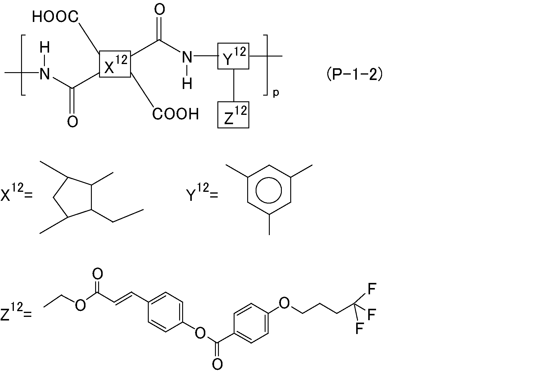
また、垂直配向膜11への配向処理工程においては、貼り合わせ後の光照射方向が互いに反平行方向になるように、直線偏光を用いた光配向処理を行った。
[比較例2]
実施例2とは異なる配向膜材料を用いたこと以外は、実施例2と同様にして比較例2の液晶パネルを作製した。比較例2では、実施例2における上記化学式(P-1-2)に示す光配向処理用の垂直配向ポリマーに替えて、下記化学式(PR-1-2)に示す光配向処理用の垂直配向ポリマーを用い、下記化学式(PR-1-2)に示す垂直配向ポリマーを含む垂直配向膜(膜厚50~160nm)を各基板上に形成した。
実施例2とは異なる配向膜材料を用いたこと以外は、実施例2と同様にして比較例2の液晶パネルを作製した。比較例2では、実施例2における上記化学式(P-1-2)に示す光配向処理用の垂直配向ポリマーに替えて、下記化学式(PR-1-2)に示す光配向処理用の垂直配向ポリマーを用い、下記化学式(PR-1-2)に示す垂直配向ポリマーを含む垂直配向膜(膜厚50~160nm)を各基板上に形成した。

[実施例2及び比較例2のバックライト上放置試験]
実施例1及び比較例1と同様の条件により、バックライト上放置試験を行った。結果を下記表2に示す。
実施例1及び比較例1と同様の条件により、バックライト上放置試験を行った。結果を下記表2に示す。

表2に示したように、垂直配向膜11に含まれる垂直配向ポリマーの側鎖が飽和脂肪族官能基である実施例2の液晶パネル1を用いた場合、初期の残留DCは条件1及び条件2共に60mVと相対的に小さかった。
また、液晶表示部2aを介してバックライト60上に実施例2の液晶パネル1を配置した条件1では、100時間放置後の残留DCは70mVであり、初期の残留DCからほとんど増加(悪化)しなかった。一方、液晶表示部2aを介さず、実施例2の液晶パネル1をバックライト60上に直接配置した条件2では、100時間放置後の残留DCは110mVまで増加した。また条件2ではVHRが95%台まで低下していることから、バックライト光によりトラン系液晶化合物のラジカル化やイオン化が進んだものと考えられる。
しかしながら、実施例2の液晶パネル1は、比較例2の液晶パネルと比べて残留DCは低い。これは、垂直配向膜11に含まれる垂直配向ポリマーの側鎖の末端を飽和脂肪族官能基とすることにより、初期及びバックライト放置後のいずれにおいても、液晶層30に含まれるトラン系液晶化合物に由来するラジカルやイオンと垂直配向膜11とのπ-π相互作用が抑制されたためと考えられる。バックライト60上に100時間放置すること等により形成された、トラン系液晶化合物に由来するラジカルやイオンは、垂直配向膜11の表面にほとんど吸着していないことを示唆していると考えられる。 また、実施例2において、バックライト60上に100時間放置した後の残留DCは、条件1の方が条件2よりも低く抑えられたのは、条件1において、実施例2の液晶パネル1とバックライト60との間に液晶表示部2aを設けたため、バックライト60からの紫外光が液晶表示部2aに効果的に吸収され、実施例2の液晶パネル1においてトラン系液晶化合物のラジカル化やイオン化の速度が遅くなったためと考えられる。
一方、比較例2の液晶パネルのように、垂直配向膜に含まれる垂直配向ポリマーとして、側鎖の末端に光官能基(シンナメート基)を持つ上記化学式(PR-1-2)で表されるポリマーを用いた場合、初期のVHRは実施例2とほとんど違いはないものの、残留DCは80mVとやや大きくなっている。さらに、液晶表示部2aを介してバックライト60上に比較例2の液晶パネルを配置した条件1では、100時間放置後の残留DCは190mVまで増加し、VHRは95.9%まで低下した。また、液晶表示部2aを介さず、比較例2の液晶パネルをバックライト60上に直接配置した条件2では、100時間放置後の残留DCは270mVまで増加し、VHRは93.2%まで低下した。このことから、垂直配向膜に含まれる垂直配向ポリマーの側鎖の末端に芳香族基を導入することで、トラン系液晶化合物に由来するラジカルやイオンと考えられる不純物が配向膜に吸着され易くなり、残留DCが増加したと考えられる。
[実施例3]
実施例2とは異なる配向膜材料及び液晶化合物を用い、かつ、配向膜の本焼成における温度を変更したこと以外は、実施例2と同様にして実施例3の液晶パネル1を作製した。実施例3では、実施例2における上記化学式(P-1-2)に示す光配向処理用の垂直配向ポリマーに替えて、下記化学式(P-5-1)に示す光配向処理用の垂直配向ポリマーを用い、下記化学式(P-5-1)に示す垂直配向ポリマーを含む垂直配向膜11(膜厚50~160nm)を各基板上に形成した。また、実施例3では垂直配向膜の本焼成を230℃に変更して行った。
実施例2とは異なる配向膜材料及び液晶化合物を用い、かつ、配向膜の本焼成における温度を変更したこと以外は、実施例2と同様にして実施例3の液晶パネル1を作製した。実施例3では、実施例2における上記化学式(P-1-2)に示す光配向処理用の垂直配向ポリマーに替えて、下記化学式(P-5-1)に示す光配向処理用の垂直配向ポリマーを用い、下記化学式(P-5-1)に示す垂直配向ポリマーを含む垂直配向膜11(膜厚50~160nm)を各基板上に形成した。また、実施例3では垂直配向膜の本焼成を230℃に変更して行った。

また、実施例3では、実施例1におけるトラン系液晶化合物と異なる、上記化学式(T)で示したトラン系液晶化合物を含有するネガ型液晶材料(Tni(液晶材料のネマティック-アイソトロピック転移点)=90℃、Δn=0.20、Δε=-3)を用いた。
[比較例3]
実施例3とは異なる配向膜材料を用いたこと以外は実施例3と同様にして、比較例3の液晶パネルを作製した。本比較例では、実施例3における上記化学式(P-5-1)に示す垂直配向ポリマーに変えて、下記化学式(PR-5-1)に示すポリマーを用い、下記化学式(PR-1-1)に示すポリマーを含む配向膜(膜厚50~160nm)を各基板上に形成した。
実施例3とは異なる配向膜材料を用いたこと以外は実施例3と同様にして、比較例3の液晶パネルを作製した。本比較例では、実施例3における上記化学式(P-5-1)に示す垂直配向ポリマーに変えて、下記化学式(PR-5-1)に示すポリマーを用い、下記化学式(PR-1-1)に示すポリマーを含む配向膜(膜厚50~160nm)を各基板上に形成した。

[実施例3及び比較例3のバックライト上放置試験]
実施例1及び比較例1と同様の条件により、バックライト上放置試験を行った。結果を下記表3に示す。
実施例1及び比較例1と同様の条件により、バックライト上放置試験を行った。結果を下記表3に示す。

表3に示したように、垂直配向膜11に含まれる垂直配向ポリマーの側鎖が飽和脂肪族官能基である実施例3の液晶パネル1を用いた場合、初期の残留DCは条件1及び条件2共に10mVと非常に小さかった。
また、液晶表示部2aを介してバックライト60上に実施例3の液晶パネル1を配置した条件1では、100時間放置後の残留DCは20mVと非常に小さく、初期の残留DCからほとんど増加(悪化)しなかった。一方、液晶表示部2aを介さず、実施例3の液晶パネル1をバックライト60上に直接配置した条件2では、100時間放置後の残留DCは60mVまで増加した。また条件2ではVHRが95%台まで低下していることから、バックライト光によりトラン系液晶化合物のラジカル化やイオン化が進んだものと考えられる。
しかしながら、実施例3の液晶パネル1は、比較例3の液晶パネルと比べて残留DCは低い。これは、垂直配向膜11に含まれる垂直配向ポリマーの側鎖の末端を飽和脂肪族官能基とすることにより、初期及びバックライト放置後のいずれにおいても、液晶層30に含まれるトラン系液晶化合物に由来するラジカルやイオンと垂直配向膜11とのπ-π相互作用が抑制されたためと考えられる。バックライト60上に100時間放置すること等により形成された、トラン系液晶化合物に由来するラジカルやイオンは、垂直配向膜11の表面にほとんど吸着していないことを示唆していると考えられる。
また、実施例3において、バックライト60上に100時間放置した後の残留DCは、条件1の方が条件2よりも低く抑えられたのは、条件1において、実施例2の液晶パネル1とバックライト60との間に液晶表示部2aを設けたため、バックライト60からの紫外光が液晶表示部2aに効果的に吸収され、実施例3の液晶パネル1においてトラン系液晶化合物のラジカル化やイオン化の速度が遅くなったためと考えられる。また、垂直配向膜11に含まれる垂直配向ポリマーの主鎖がポリイミド構造である実施例2の液晶パネルと、主鎖がシロキサン構造である実施例3の液晶パネルとを比較すると、実施例3の方が残留DCをより低く抑えられていることから、垂直配向膜11に含まれる垂直配向ポリマーの主鎖をシロキサン構造にすることにより、残留DCを低く抑えることが可能であることが分かった。
一方、比較例3の液晶パネルのように、垂直配向膜に含まれる垂直配向ポリマーとして、側鎖の末端に光官能基(シンナメート基)を持つ上記化学式(PR-5-1)で表されるポリマーを用いた場合、初期のVHRは実施例3とほとんど違いはないものの、残留DCは30mVまで大きくなっている。さらに、液晶表示部2aを介してバックライト60上に比較例3の液晶パネルを配置した条件1では、100時間放置後の残留DCは110mVまで増加し、VHRは96.3%まで低下した。また、液晶表示部2aを介さず、比較例3の液晶パネルをバックライト60上に直接配置した条件2では、100時間放置後の残留DCは190mVまで増加し、VHRは94.2%まで低下した。このことから、垂直配向膜に含まれる垂直配向ポリマーの側鎖の末端に芳香族基を導入することで、トラン系液晶化合物に由来するラジカルやイオンと考えられる不純物が配向膜に吸着され易くなり、残留DCが増加したと考えられる。また、配向膜に含まれる高分子の主鎖がポリイミド構造である比較例2の液晶パネルと、高分子の主鎖がシロキサン構造である比較例3の液晶パネルとを比較すると、比較例3の方が、残留DCをより低く抑えられていることから、配向膜に含まれる高分子の主鎖をシロキサン構造にすることにより、残留DCを低く抑えることが可能であることが分かった。
[実施例4]
実施例4では、以下の方法により、実施形態3のスイッチャブル・ミラーディスプレイ3を作製した。
実施例4では、以下の方法により、実施形態3のスイッチャブル・ミラーディスプレイ3を作製した。
まず、パッシブ駆動型のスイッチャブル・ミラーパネル2を次の手順で作製した。ITO電極を有する一対の基板(背面側:第一基板10、前面側(観測者側):第二基板20)を用意し、下記化学式(P-1-1)に示す垂直配向ポリマーを含有する溶剤を、各基板10、20上に塗布し、90℃、5分の仮焼成を行い、続いて200℃、40分の本焼成を行った。焼成処理を行うことで、高分子主鎖がポリイミドであり、高分子側鎖の末端が飽和脂肪族官能基である下記化学式(P-1-1)に示す垂直配向ポリマーを含む垂直配向膜11(膜厚50~160nm)を形成した。

続いて、各垂直配向膜11に、貼り合わせ後のラビング方向が互いに反平行方向になるようにラビング処理を施した。次に、第二基板20に、ディスペンサを使用して紫外線硬化性シール剤(積水化学工業社製、商品名:フォトレックS-WB)を描画した。また、第一基板10上の所定の位置に、上記化学式(T)で示したトラン系液晶化合物を含有するネガ型液晶材料(Tni(液晶材料のネマティック-アイソトロピック転移点)=90℃、Δn=0.19、Δε=-5)を滴下した。
続いて、真空下にて両基板10、20を貼り合わせ、シール剤を紫外光にて硬化させた。このようにして得られた液晶セルにおける液晶化合物の流動配向を消すために、液晶セルを130℃で40分間加熱し、液晶を等方相にする再配向処理を行い、その後室温まで冷却してVA-ECBモードの液晶パネル1を得た。
得られた液晶パネル1の第二基板20の液晶層30とは反対側の面に吸収型偏光板50を貼り、第一基板10の液晶層30とは反対側の面に反射型偏光板40(スリーエム社製、DBEF(登録商標))を貼り、スイッチャブル・ミラーパネル2を得た。なお、吸収型偏光板は、ポリビニルアルコール(PVA)フィルムに二色性を有するヨウ素錯体等の異方性材料を吸着配向させたものを用いた。
液晶表示部2aは、シャープ社製のFFSモードの表示用液晶パネル1aの背面側に吸収型偏光板50aを配置し、前面側に吸収型偏光板50bを配置して作製した。すなわち、液晶表示部2aは、アクティブ基板10bと、カラーフィルタ基板20bと、アクティブ基板10b及びカラーフィルタ基板20bに挟持された液晶層30aと、アクティブ基板10b及びカラーフィルタ基板20bの液晶層30aとは反対側に設けられた吸収型偏光板50a、50bとを備えている。液晶表示部2aにおけるアクティブ基板10b及びカラーフィルタ基板20bは、互いに反平行方向にラビング処理されており、液晶層30aの液晶化合物は水平に配向している。また、液晶表示部2aを構成する2枚の基板10a、20aのうちの一方には、窒化膜などの透明絶縁膜を介し、スリットが設けられた上層画素電極と、スリットが設けられていない下層画素電極とが形成されている。上層及び下層画素電極の間に電圧を印加することで、フリンジ電界が発生する。FFSモードは、このフリンジ電界により、液晶化合物の配向方向を基板面内で変化させて、透過光量を変化させる表示モードである。
最後に、バックライト60、液晶表示部2a及びスイッチャブル・ミラーパネル2をこの順で積層することにより、スイッチャブル・ミラーディスプレイ3を作製した。なお、本実施例は、液晶表示部2aとスイッチャブル・ミラーパネル2とを空気層を介して積層しただけであるが、OCA等により接着しても良い。また、液晶表示部2aの代わりに、反射防止用の吸収型円偏光板が設けられた有機エレクトロルミネッセンス表示装置、偏光板が貼り付けられたMEMSディスプレイ等の、偏光を出射する表示装置を用いることもできる。
図5は、実施例4のスイッチャブル・ミラーディスプレイにおける偏光状態を示した図であり、(1)はスイッチャブル・ミラーパネルの前面側の吸収型偏光板に関する図であり、(2)はスイッチャブル・ミラーパネルの液晶パネルに関する図であり、(3)はスイッチャブル・ミラーパネルの背面側の反射型偏光板に関する図であり、(4)は、液晶表示部の前面側の吸収型偏光板に関する図であり、(5)は液晶表示部のFFSモードの表示用液晶パネルに関する図であり、(6)は液晶表示部の背面側の吸収型偏光板に関する図である。図5(1)、(4)及び(6)における実線の矢印は透過軸を表し、破線の矢印は吸収軸を表す。図5(2)及び(5)における実線の矢印は前面側の基板のラビング方向を表し、破線の矢印は背面側の基板のラビング方向し、前面側及び背面側のいずれの基板も45°方向にラビングされている。図5(3)における実線の矢印は反射型偏光板の透過軸を表し、破線の矢印は反射軸を表す。
実施例4で作製したスイッチャブル・ミラーディスプレイ3で用いた各偏光板の透過軸について説明する。図5(1)~(6)に示すように、実施例4のスイッチャブル・ミラーディスプレイ3では、スイッチャブル・ミラーパネル2における反射型偏光板40の透過軸と吸収型偏光板50の透過軸とは平行であり、液晶表示部2aにおける吸収型偏光板50aの透過軸と吸収型偏光板50bの透過軸とは直交し、スイッチャブル・ミラーパネル2における反射型偏光板40の透過軸と液晶表示部2aにおける吸収型偏光板50bの透過軸とは平行である。これにより、スイッチャブル・ミラーパネル2は、電圧無印加状態の時に透明モードとなるため、液晶表示部2aの画像を表示することが可能となる。また、スイッチャブル・ミラーパネル2は、電圧印加状態の時にミラーモードとなるため、反射光による鏡像が視認可能である。
実施例4で作製したスイッチャブル・ミラーディスプレイ3の動作について、更に説明する。
<電圧無印加時の動作>
スイッチャブル・ミラーパネル2は、電圧無印加状態の時、FFSモードの表示用液晶パネル1aが設けられた液晶表示部2aの前面(観測者)側の吸収型偏光板50bを出射した直線偏光は、VA-ECBモードの液晶パネル1が設けられたスイッチャブル・ミラーパネル2の反射型偏光板40の透過軸を通過する。スイッチャブル・ミラーパネル2におけるVA-ECBモードの液晶パネル1の位相差(複屈折性)はゼロであるので、反射型偏光板40の透過光は、偏光状態を維持した状態で、スイッチャブル・ミラーパネル2の前面(観測者)側の吸収型偏光板50の透過軸を通過し、観測者の目に到達する。すなわち、スイッチャブル・ミラーパネル2を構成するVA-ECBモードの液晶パネル1や反射型偏光板40、吸収型偏光板50があるにも関わらず、観察者はそれらが無かった場合と同様に液晶表示部2aにおけるFFSモードの表示用液晶パネル1aの表示を見ることができる。
スイッチャブル・ミラーパネル2は、電圧無印加状態の時、FFSモードの表示用液晶パネル1aが設けられた液晶表示部2aの前面(観測者)側の吸収型偏光板50bを出射した直線偏光は、VA-ECBモードの液晶パネル1が設けられたスイッチャブル・ミラーパネル2の反射型偏光板40の透過軸を通過する。スイッチャブル・ミラーパネル2におけるVA-ECBモードの液晶パネル1の位相差(複屈折性)はゼロであるので、反射型偏光板40の透過光は、偏光状態を維持した状態で、スイッチャブル・ミラーパネル2の前面(観測者)側の吸収型偏光板50の透過軸を通過し、観測者の目に到達する。すなわち、スイッチャブル・ミラーパネル2を構成するVA-ECBモードの液晶パネル1や反射型偏光板40、吸収型偏光板50があるにも関わらず、観察者はそれらが無かった場合と同様に液晶表示部2aにおけるFFSモードの表示用液晶パネル1aの表示を見ることができる。
この時、観察者側から入射する外光は、スイッチャブル・ミラーパネル2における吸収型偏光板50を通ることで直線偏光となり、複屈折の影響を受けずに、すなわち、直線偏光を維持したままスイッチャブル・ミラーパネル2における反射型偏光板40に到達する。スイッチャブル・ミラーパネル2における反射型偏光板40の透過軸とスイッチャブル・ミラーパネル2における吸収型偏光板50の透過軸とは平行であるため、反射型偏光板40に到達した直線偏光は反射型偏光板40で反射されることなく反射型偏光板40を透過する。その後、液晶表示部2aにおける吸収型偏光板50b及びFFSモードの液晶セル1a等を通って背面側に向かって進むが、最も背面側に位置する液晶表示部2aにおける吸収型偏光板50a、或いは、FFSモードの表示用液晶パネル1aが含有するカラーフィルタやブラックマスクなどの吸収体により吸収されるため、再び観察者側に反射光として戻る成分は殆どない。
このように、VA-ECBモードの液晶パネル1を有するスイッチャブル・ミラーパネル2が電圧無印加状態である時、観察者はFFSモードの表示用液晶パネル1aが設けられた液晶表示部2aの表示を見ることが可能であり、外光が反射型偏光板によって不要反射となり明所での視認性を低下させることもない。
<電圧印加時の動作>
VA-ECBモードの液晶パネル1が設けられたスイッチャブル・ミラーパネル2に電圧を印加するのはミラーモードとして動作をさせる時である。ミラーモードとしての機能、動作が重要であるため、FFSモードの表示用液晶パネル1aが設けられた液晶表示部2aは、ミラーモードの際に全体或いは部分的に表示を行わない(黒表示を行う、或いは、バックライトを消灯又は減光する)ことが好ましい。
VA-ECBモードの液晶パネル1が設けられたスイッチャブル・ミラーパネル2に電圧を印加するのはミラーモードとして動作をさせる時である。ミラーモードとしての機能、動作が重要であるため、FFSモードの表示用液晶パネル1aが設けられた液晶表示部2aは、ミラーモードの際に全体或いは部分的に表示を行わない(黒表示を行う、或いは、バックライトを消灯又は減光する)ことが好ましい。
VA-ECBモードの液晶パネル1が設けられたスイッチャブル・ミラーパネル2に、前面(観察者)側から入射する外光は、スイッチャブル・ミラーパネル2における吸収型偏光板50を通ることで直線偏光となり、VA-ECBモードの液晶パネル1の複屈折性により楕円偏光に変換された後、スイッチャブル・ミラーパネル2における反射型偏光板40に到達する。この楕円偏光の振動成分のうち、反射型偏光板の40透過軸と平行な方向に振動する偏光成分は背面側に通り抜け、その後、液晶表示部2aに設けられたFFSモードの表示用液晶パネル1aで吸収される。スイッチャブル・ミラーパネル2における反射型偏光板40の反射軸と平行な方向に振動する成分は前面(観察者)側に直線偏光として反射され、再度、VA-ECBモードの液晶パネル1の複屈折性により楕円偏光に変換された後、スイッチャブル・ミラーパネル2における吸収型偏光板50に到達する。スイッチャブル・ミラーパネル2における吸収型偏光板50の透過軸と平行な偏光成分はそのまま前面(観察者)側に通り抜け、観察者の目に反射光として届くことになる。スイッチャブル・ミラーパネル2における吸収型偏光板50の透過軸と直交する(吸収軸と平行な)偏光成分は吸収される。
複屈折性による偏光状態の変化やそれと関係する透過率や反射率の変化は波長分散(波長依存性)が大きいため、反射光の強度は波長によって異なることになり、すなわち、実施例4のスイッチャブルブルミラーディスプレイ3における外光反射は色づいて見える。
[実施例4のバックライト上放置試験]
まず、実施例4にて作製したスイッチャブル・ミラーディスプレイ3のバックライト60を点灯する前に、実施例1と同様の方法を用いて、実施例4にて作製したスイッチャブル・ミラーディスプレイ3におけるスイッチャブル・ミラーパネル2の初期の残留DC及びVHRを測定した。
まず、実施例4にて作製したスイッチャブル・ミラーディスプレイ3のバックライト60を点灯する前に、実施例1と同様の方法を用いて、実施例4にて作製したスイッチャブル・ミラーディスプレイ3におけるスイッチャブル・ミラーパネル2の初期の残留DC及びVHRを測定した。
続いて、実施例4にて作製したスイッチャブル・ミラーディスプレイ3のバックライト60を点灯し、100時間放置した後、上記と同様にスイッチャブル・ミラーパネル2の残留DC及びVHRを測定した。結果を下記表4に示す。

実施例4のスイッチャブル・ミラーパネル2における初期の残留DCは20mVと小さく、また、100時間バックライト上に放置した後の残留DCは30mVであり、初期の残留DCからほとんど増加(悪化)しなかった。
更に、実施例4のスイッチャブル・ミラーパネル2における初期のVHRは98.3%であり、また、100時間バックライト上に放置した後のVHRは97.4%であり、バックライト上に放置する前後でのVHRはほとんど変わらず、高い値を維持していた。
以上のように、実施例4のスイッチャブル・ミラーパネル2は、実施例1の液晶パネル1と同等の低い残留DC及び高いVHRを有していた。実施例4のスイッチャブル・ミラーパネル2には、トラン系液晶化合物と共に、側鎖の末端に飽和脂肪族官能基を有する垂直配向ポリマーが用いられているため、初期及びバックライト放置後のいずれにおいても、液晶層30に含まれるトラン系液晶化合物に由来するラジカルやイオンと配向膜11とのπ-π相互作用が抑制されたため、低い残留DC及び高いVHRを得ることができたと考えられる。また、実施例4のスイッチャブル・ミラーディスプレイ3は、スイッチャブル・ミラーパネル2とバックライト60との間に、液晶表示部2aを有しているため、バックライト60からの紫外光が液晶表示部2aに効果的に吸収され、実施例4のスイッチャブル・ミラーパネル2においてトラン系液晶化合物のラジカル化やイオン化の速度が遅くなったと考えられる。このことも、残留DCを低く抑え、VHRを高く維持することができた理由の1つと考えられる。
1:液晶パネル
1a:表示用液晶パネル
2:スイッチャブル・ミラーパネル
2a:液晶表示部
3:スイッチャブル・ミラーディスプレイ
10:第一基板
10a、20a:基板
10b:アクティブ基板
11:垂直配向膜
11a:配向膜
20:第二基板
20b:カラーフィルタ基板
30、30a:液晶層
40:反射型偏光板
50、50a、50b:吸収型偏光板
60:バックライト
1a:表示用液晶パネル
2:スイッチャブル・ミラーパネル
2a:液晶表示部
3:スイッチャブル・ミラーディスプレイ
10:第一基板
10a、20a:基板
10b:アクティブ基板
11:垂直配向膜
11a:配向膜
20:第二基板
20b:カラーフィルタ基板
30、30a:液晶層
40:反射型偏光板
50、50a、50b:吸収型偏光板
60:バックライト
Claims (12)
- 第一基板と、第二基板と、前記第一基板及び前記第二基板に挟持された液晶層と、前記第一基板及び前記第二基板の前記液晶層側に設けられた垂直配向膜とを備え、
前記液晶層は、負の誘電率異方性を有する液晶材料からなり、
前記液晶材料は、トラン系液晶化合物を含み、
前記垂直配向膜は、主鎖及び側鎖を有する垂直配向ポリマーを含み、前記側鎖の末端は、飽和脂肪族官能基を有することを特徴とする液晶パネル。 - 前記トラン系液晶化合物は、下記化学式(T)で表される化合物であることを特徴とする請求項1に記載の液晶パネル。
- 前記化学式(T)におけるR1及びR2は各々独立に、-CH3、-C2H5、-C3H7、-C4H9、-C5H11、-C6H13、-OCH3、-OC2H5、-OC3H7、-OC4H9、-OC5H11、-OC6H13、-C2H4CH=CH2又は-OC2H4CH=CH2を表し、R31及びR32は各々独立にフッ素原子を表し、a1及びa2は各々独立に0~2の整数を表すことを特徴とする請求項2に記載の液晶パネル。
- 前記トラン系液晶化合物は、下記化学式(T-1)~(T-5)で表される液晶化合物からなる群より選択される少なくとも一種の液晶化合物であることを特徴とする請求項1~3のいずれかに記載の液晶パネル。

- 前記液晶材料の複屈折率Δnは0.18以上であり、且つ、誘電率異方性Δεは-2.5以下であることを特徴とする請求項1~4のいずれかに記載の液晶パネル。
- 前記垂直配向ポリマーの前記側鎖は、下記化学式(ZA-1)~(ZA-8)で表される基からなる群より選択される少なくとも1つの基を有することを特徴とする請求項1~5のいずれかに記載の液晶パネル。

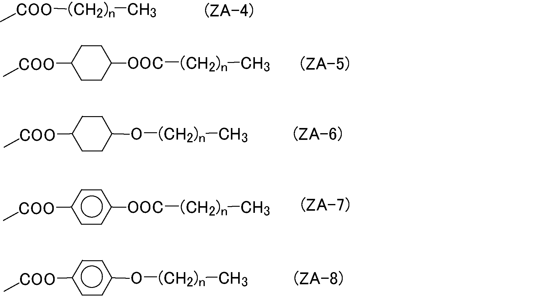
- 前記垂直配向ポリマーの前記主鎖は、ポリアミック酸、ポリイミド、ポリシロキサン又はポリビニルを有することを特徴とする請求項1~6のいずれかに記載の液晶パネル。
- 前記垂直配向膜は、光配向膜であることを特徴とする請求項1~7のいずれかに記載の液晶パネル。
- 前記垂直配向ポリマーの前記側鎖は、シンナメート基、アゾベンゼン基、カルコン基、クマリン基及びスチルベン基からなる群より選択される少なくとも1種の基を有することを特徴とする請求項8に記載の液晶パネル。
- 前記液晶パネルは、パッシブ駆動型であることを特徴とする請求項1~9のいずれかに記載の液晶パネル。
- 背面側から前面側に向かって順に、
反射型偏光板と、請求項1~10のいずれかに記載の液晶パネルと、吸収型偏光板とを備え、
前記反射型偏光板の背面側からの入射光が前記吸収型偏光板を透過する透明モードと、前記吸収型偏光板の前面側からの入射光が前記反射型偏光板で反射されるミラーモードとに切り換え可能であることを特徴とするスイッチャブル・ミラーパネル。 - 背面側から前面側に向かって順に、バックライトと、液晶表示部と、請求項11に記載のスイッチャブル・ミラーパネルとを備え、
前記液晶表示部は、アクティブ基板と、カラーフィルタ基板と、前記アクティブ基板及びカラーフィルタ基板に挟持された液晶層と、前記アクティブ基板及びカラーフィルタ基板の前記液晶層とは反対側に設けられた偏光板とを備えることを特徴とするスイッチャブル・ミラーディスプレイ。
Priority Applications (1)
| Application Number | Priority Date | Filing Date | Title |
|---|---|---|---|
| US16/305,872 US20190219856A1 (en) | 2016-05-31 | 2017-05-24 | Liquid crystal panel, switchable mirror panel and switchable mirror display |
Applications Claiming Priority (2)
| Application Number | Priority Date | Filing Date | Title |
|---|---|---|---|
| JP2016-109025 | 2016-05-31 | ||
| JP2016109025 | 2016-05-31 |
Publications (1)
| Publication Number | Publication Date |
|---|---|
| WO2017208914A1 true WO2017208914A1 (ja) | 2017-12-07 |
Family
ID=60477444
Family Applications (1)
| Application Number | Title | Priority Date | Filing Date |
|---|---|---|---|
| PCT/JP2017/019296 Ceased WO2017208914A1 (ja) | 2016-05-31 | 2017-05-24 | 液晶パネル、スイッチャブル・ミラーパネル及びスイッチャブル・ミラーディスプレイ |
Country Status (2)
| Country | Link |
|---|---|
| US (1) | US20190219856A1 (ja) |
| WO (1) | WO2017208914A1 (ja) |
Cited By (2)
| Publication number | Priority date | Publication date | Assignee | Title |
|---|---|---|---|---|
| JP2020194013A (ja) * | 2019-05-24 | 2020-12-03 | スタンレー電気株式会社 | 機能選択複合光学装置 |
| WO2025069978A1 (ja) * | 2023-09-26 | 2025-04-03 | 株式会社ジャパンディスプレイ | 照明装置 |
Families Citing this family (3)
| Publication number | Priority date | Publication date | Assignee | Title |
|---|---|---|---|---|
| DE112018005192T5 (de) * | 2017-11-01 | 2020-06-18 | Murakami Corporation | Bildanzeigesystem |
| JP7325026B2 (ja) * | 2020-02-19 | 2023-08-14 | santec Holdings株式会社 | 光学システム |
| US11852952B2 (en) * | 2021-10-27 | 2023-12-26 | Sharp Display Technology Corporation | Liquid crystal lens, head mounted display and polarized sunglasses |
Citations (3)
| Publication number | Priority date | Publication date | Assignee | Title |
|---|---|---|---|---|
| JP3419766B2 (ja) * | 2000-02-29 | 2003-06-23 | 株式会社日立製作所 | 画像表示状態と鏡状態とを切り替え可能な装置、および、これを備えた機器 |
| JP2005213320A (ja) * | 2004-01-28 | 2005-08-11 | Dainippon Ink & Chem Inc | ネマチック液晶組成物およびこれを用いた液晶表示素子 |
| JP2011227484A (ja) * | 2010-03-31 | 2011-11-10 | Dic Corp | 垂直配向層用組成物 |
-
2017
- 2017-05-24 US US16/305,872 patent/US20190219856A1/en not_active Abandoned
- 2017-05-24 WO PCT/JP2017/019296 patent/WO2017208914A1/ja not_active Ceased
Patent Citations (3)
| Publication number | Priority date | Publication date | Assignee | Title |
|---|---|---|---|---|
| JP3419766B2 (ja) * | 2000-02-29 | 2003-06-23 | 株式会社日立製作所 | 画像表示状態と鏡状態とを切り替え可能な装置、および、これを備えた機器 |
| JP2005213320A (ja) * | 2004-01-28 | 2005-08-11 | Dainippon Ink & Chem Inc | ネマチック液晶組成物およびこれを用いた液晶表示素子 |
| JP2011227484A (ja) * | 2010-03-31 | 2011-11-10 | Dic Corp | 垂直配向層用組成物 |
Cited By (3)
| Publication number | Priority date | Publication date | Assignee | Title |
|---|---|---|---|---|
| JP2020194013A (ja) * | 2019-05-24 | 2020-12-03 | スタンレー電気株式会社 | 機能選択複合光学装置 |
| JP7405520B2 (ja) | 2019-05-24 | 2023-12-26 | スタンレー電気株式会社 | 機能選択複合光学装置 |
| WO2025069978A1 (ja) * | 2023-09-26 | 2025-04-03 | 株式会社ジャパンディスプレイ | 照明装置 |
Also Published As
| Publication number | Publication date |
|---|---|
| US20190219856A1 (en) | 2019-07-18 |
Similar Documents
| Publication | Publication Date | Title |
|---|---|---|
| KR101643212B1 (ko) | 편광판, 표시 장치 및 전자 기기 | |
| WO2017208914A1 (ja) | 液晶パネル、スイッチャブル・ミラーパネル及びスイッチャブル・ミラーディスプレイ | |
| KR20170072270A (ko) | 중합체를 함유하는 산란형 수직 배향 액정 장치 | |
| TWI518420B (zh) | 液晶顯示元件的製造方法及液晶顯示元件 | |
| CN104662469B (zh) | 液晶显示装置及其制造方法 | |
| TWI524116B (zh) | A liquid crystal display panel, a liquid crystal display device, and a liquid crystal display unit | |
| JP2012220673A (ja) | 液晶光学装置、及びその製造方法 | |
| WO2018008583A1 (ja) | 液晶表示装置、及び、液晶表示装置の製造方法 | |
| WO2018216605A1 (ja) | 液晶組成物、液晶表示装置、及び、液晶表示装置の製造方法 | |
| WO1992014180A1 (fr) | Matiere optique anisotrope, sa fabrication, dispositif a cristaux liquides dote de ladite matiere et sa production | |
| KR102354935B1 (ko) | 광변조 소자 | |
| WO2019009222A1 (ja) | 液晶組成物、液晶表示装置、及び、液晶表示装置の製造方法 | |
| US8537326B2 (en) | Liquid crystal composition, device and method thereof | |
| KR102290713B1 (ko) | 광변조 소자 | |
| CN110678807B (zh) | 液晶显示装置及液晶显示装置的制造方法 | |
| CN110678788B (zh) | 液晶显示装置、液晶显示装置的制造方法、及相位差层形成用单体 | |
| US10551678B2 (en) | Liquid crystal display device | |
| US20190212616A1 (en) | Liquid crystal display device and method for producing liquid crystal display device | |
| CN115561939B (zh) | 液晶显示装置 | |
| US11988918B1 (en) | Optical element and display device | |
| US9170460B2 (en) | In-plane-switching mode liquid crystal panel, manufacturing process and display device thereof | |
| WO2019009166A1 (ja) | 液晶表示装置及び液晶表示装置の製造方法 | |
| CN110244494A (zh) | 液晶显示装置、其制造方法及相位差层用单体材料 | |
| US20190346607A1 (en) | Retardation substrate, liquid crystal element and liquid crystal module | |
| JP2023146598A (ja) | 液晶表示装置 |
Legal Events
| Date | Code | Title | Description |
|---|---|---|---|
| 121 | Ep: the epo has been informed by wipo that ep was designated in this application |
Ref document number: 17806471 Country of ref document: EP Kind code of ref document: A1 |
|
| NENP | Non-entry into the national phase |
Ref country code: DE |
|
| 122 | Ep: pct application non-entry in european phase |
Ref document number: 17806471 Country of ref document: EP Kind code of ref document: A1 |
|
| NENP | Non-entry into the national phase |
Ref country code: JP |