WO2017209191A1 - 半導体パワーモジュール - Google Patents
半導体パワーモジュール Download PDFInfo
- Publication number
- WO2017209191A1 WO2017209191A1 PCT/JP2017/020303 JP2017020303W WO2017209191A1 WO 2017209191 A1 WO2017209191 A1 WO 2017209191A1 JP 2017020303 W JP2017020303 W JP 2017020303W WO 2017209191 A1 WO2017209191 A1 WO 2017209191A1
- Authority
- WO
- WIPO (PCT)
- Prior art keywords
- terminal
- insulating substrate
- power supply
- supply terminal
- switching element
- Prior art date
- Legal status (The legal status is an assumption and is not a legal conclusion. Google has not performed a legal analysis and makes no representation as to the accuracy of the status listed.)
- Ceased
Links
Images


Classifications
-
- B—PERFORMING OPERATIONS; TRANSPORTING
- B41—PRINTING; LINING MACHINES; TYPEWRITERS; STAMPS
- B41J—TYPEWRITERS; SELECTIVE PRINTING MECHANISMS, i.e. MECHANISMS PRINTING OTHERWISE THAN FROM A FORME; CORRECTION OF TYPOGRAPHICAL ERRORS
- B41J5/00—Devices or arrangements for controlling character selection
- B41J5/30—Character or syllable selection controlled by recorded information
-
- H—ELECTRICITY
- H02—GENERATION; CONVERSION OR DISTRIBUTION OF ELECTRIC POWER
- H02M—APPARATUS FOR CONVERSION BETWEEN AC AND AC, BETWEEN AC AND DC, OR BETWEEN DC AND DC, AND FOR USE WITH MAINS OR SIMILAR POWER SUPPLY SYSTEMS; CONVERSION OF DC OR AC INPUT POWER INTO SURGE OUTPUT POWER; CONTROL OR REGULATION THEREOF
- H02M7/00—Conversion of AC power input into DC power output; Conversion of DC power input into AC power output
- H02M7/003—Constructional details, e.g. physical layout, assembly, wiring or busbar connections
-
- H—ELECTRICITY
- H02—GENERATION; CONVERSION OR DISTRIBUTION OF ELECTRIC POWER
- H02M—APPARATUS FOR CONVERSION BETWEEN AC AND AC, BETWEEN AC AND DC, OR BETWEEN DC AND DC, AND FOR USE WITH MAINS OR SIMILAR POWER SUPPLY SYSTEMS; CONVERSION OF DC OR AC INPUT POWER INTO SURGE OUTPUT POWER; CONTROL OR REGULATION THEREOF
- H02M7/00—Conversion of AC power input into DC power output; Conversion of DC power input into AC power output
- H02M7/42—Conversion of DC power input into AC power output without possibility of reversal
- H02M7/44—Conversion of DC power input into AC power output without possibility of reversal by static converters
- H02M7/48—Conversion of DC power input into AC power output without possibility of reversal by static converters using discharge tubes with control electrode or semiconductor devices with control electrode
-
- H—ELECTRICITY
- H10—SEMICONDUCTOR DEVICES; ELECTRIC SOLID-STATE DEVICES NOT OTHERWISE PROVIDED FOR
- H10W—GENERIC PACKAGES, INTERCONNECTIONS, CONNECTORS OR OTHER CONSTRUCTIONAL DETAILS OF DEVICES COVERED BY CLASS H10
- H10W40/00—Arrangements for thermal protection or thermal control
- H10W40/10—Arrangements for heating
-
- H—ELECTRICITY
- H10—SEMICONDUCTOR DEVICES; ELECTRIC SOLID-STATE DEVICES NOT OTHERWISE PROVIDED FOR
- H10W—GENERIC PACKAGES, INTERCONNECTIONS, CONNECTORS OR OTHER CONSTRUCTIONAL DETAILS OF DEVICES COVERED BY CLASS H10
- H10W72/00—Interconnections or connectors in packages
- H10W72/20—Bump connectors, e.g. solder bumps or copper pillars; Dummy bumps; Thermal bumps
-
- H—ELECTRICITY
- H10—SEMICONDUCTOR DEVICES; ELECTRIC SOLID-STATE DEVICES NOT OTHERWISE PROVIDED FOR
- H10W—GENERIC PACKAGES, INTERCONNECTIONS, CONNECTORS OR OTHER CONSTRUCTIONAL DETAILS OF DEVICES COVERED BY CLASS H10
- H10W90/00—Package configurations
-
- H—ELECTRICITY
- H10—SEMICONDUCTOR DEVICES; ELECTRIC SOLID-STATE DEVICES NOT OTHERWISE PROVIDED FOR
- H10W—GENERIC PACKAGES, INTERCONNECTIONS, CONNECTORS OR OTHER CONSTRUCTIONAL DETAILS OF DEVICES COVERED BY CLASS H10
- H10W72/00—Interconnections or connectors in packages
- H10W72/071—Connecting or disconnecting
- H10W72/075—Connecting or disconnecting of bond wires
- H10W72/07551—Connecting or disconnecting of bond wires characterised by changes in properties of the bond wires during the connecting
- H10W72/07552—Connecting or disconnecting of bond wires characterised by changes in properties of the bond wires during the connecting changes in structures or sizes
-
- H—ELECTRICITY
- H10—SEMICONDUCTOR DEVICES; ELECTRIC SOLID-STATE DEVICES NOT OTHERWISE PROVIDED FOR
- H10W—GENERIC PACKAGES, INTERCONNECTIONS, CONNECTORS OR OTHER CONSTRUCTIONAL DETAILS OF DEVICES COVERED BY CLASS H10
- H10W72/00—Interconnections or connectors in packages
- H10W72/071—Connecting or disconnecting
- H10W72/075—Connecting or disconnecting of bond wires
- H10W72/07551—Connecting or disconnecting of bond wires characterised by changes in properties of the bond wires during the connecting
- H10W72/07554—Connecting or disconnecting of bond wires characterised by changes in properties of the bond wires during the connecting changes in dispositions
-
- H—ELECTRICITY
- H10—SEMICONDUCTOR DEVICES; ELECTRIC SOLID-STATE DEVICES NOT OTHERWISE PROVIDED FOR
- H10W—GENERIC PACKAGES, INTERCONNECTIONS, CONNECTORS OR OTHER CONSTRUCTIONAL DETAILS OF DEVICES COVERED BY CLASS H10
- H10W72/00—Interconnections or connectors in packages
- H10W72/50—Bond wires
- H10W72/521—Structures or relative sizes of bond wires
- H10W72/527—Multiple bond wires having different sizes
-
- H—ELECTRICITY
- H10—SEMICONDUCTOR DEVICES; ELECTRIC SOLID-STATE DEVICES NOT OTHERWISE PROVIDED FOR
- H10W—GENERIC PACKAGES, INTERCONNECTIONS, CONNECTORS OR OTHER CONSTRUCTIONAL DETAILS OF DEVICES COVERED BY CLASS H10
- H10W72/00—Interconnections or connectors in packages
- H10W72/50—Bond wires
- H10W72/541—Dispositions of bond wires
- H10W72/5445—Dispositions of bond wires being orthogonal to a side surface of the chip, e.g. parallel arrangements
-
- H—ELECTRICITY
- H10—SEMICONDUCTOR DEVICES; ELECTRIC SOLID-STATE DEVICES NOT OTHERWISE PROVIDED FOR
- H10W—GENERIC PACKAGES, INTERCONNECTIONS, CONNECTORS OR OTHER CONSTRUCTIONAL DETAILS OF DEVICES COVERED BY CLASS H10
- H10W72/00—Interconnections or connectors in packages
- H10W72/50—Bond wires
- H10W72/541—Dispositions of bond wires
- H10W72/547—Dispositions of multiple bond wires
-
- H—ELECTRICITY
- H10—SEMICONDUCTOR DEVICES; ELECTRIC SOLID-STATE DEVICES NOT OTHERWISE PROVIDED FOR
- H10W—GENERIC PACKAGES, INTERCONNECTIONS, CONNECTORS OR OTHER CONSTRUCTIONAL DETAILS OF DEVICES COVERED BY CLASS H10
- H10W72/00—Interconnections or connectors in packages
- H10W72/851—Dispositions of multiple connectors or interconnections
- H10W72/874—On different surfaces
- H10W72/884—Die-attach connectors and bond wires
-
- H—ELECTRICITY
- H10—SEMICONDUCTOR DEVICES; ELECTRIC SOLID-STATE DEVICES NOT OTHERWISE PROVIDED FOR
- H10W—GENERIC PACKAGES, INTERCONNECTIONS, CONNECTORS OR OTHER CONSTRUCTIONAL DETAILS OF DEVICES COVERED BY CLASS H10
- H10W72/00—Interconnections or connectors in packages
- H10W72/90—Bond pads, in general
- H10W72/921—Structures or relative sizes of bond pads
- H10W72/926—Multiple bond pads having different sizes
-
- H—ELECTRICITY
- H10—SEMICONDUCTOR DEVICES; ELECTRIC SOLID-STATE DEVICES NOT OTHERWISE PROVIDED FOR
- H10W—GENERIC PACKAGES, INTERCONNECTIONS, CONNECTORS OR OTHER CONSTRUCTIONAL DETAILS OF DEVICES COVERED BY CLASS H10
- H10W74/00—Encapsulations, e.g. protective coatings
-
- H—ELECTRICITY
- H10—SEMICONDUCTOR DEVICES; ELECTRIC SOLID-STATE DEVICES NOT OTHERWISE PROVIDED FOR
- H10W—GENERIC PACKAGES, INTERCONNECTIONS, CONNECTORS OR OTHER CONSTRUCTIONAL DETAILS OF DEVICES COVERED BY CLASS H10
- H10W90/00—Package configurations
- H10W90/701—Package configurations characterised by the relative positions of pads or connectors relative to package parts
- H10W90/751—Package configurations characterised by the relative positions of pads or connectors relative to package parts of bond wires
- H10W90/753—Package configurations characterised by the relative positions of pads or connectors relative to package parts of bond wires between laterally-adjacent chips
Definitions
- the present invention relates to a semiconductor power module.
- Patent Document 1 discloses an inverter module as an example of a semiconductor power module including a plurality of switching elements.
- the inverter module includes a first semiconductor element (first switching element), a second semiconductor element (second switching element), and a resin case that houses them.
- a positive terminal (power terminal) connected to the first semiconductor element and a negative terminal (power terminal) connected to the second semiconductor element are spaced at one end of the resin case. It is arranged with a gap.
- a pair of output side terminals connected in common to the first semiconductor element and the second semiconductor element are disposed at the other end of the resin case.
- a semiconductor power module including a plurality of switching elements has a problem that a surge voltage may be generated during a switching operation. Since the magnitude of the surge voltage is proportional to the inductance component of a current path such as a wiring through which a current flows, it is an issue to remove the inductance component from the current path.
- the distance between these two power terminals is set depending on the shape of the resin case, it is a relatively large value. For this reason, the magnetic field generated at one power supply terminal and the magnetic field generated at the other power supply terminal cannot be offset well, and the mutual inductance component between the terminals may increase due to the mutual induction effect. .
- the present invention provides a semiconductor power module that can reduce the inductance component.
- the present invention includes an insulating substrate having one surface and the other surface, an output-side terminal disposed on the one surface side of the insulating substrate, a first power supply terminal disposed on the one surface side of the insulating substrate, A voltage having a magnitude different from the voltage applied to the first power supply terminal is applied to the other surface of the insulating substrate so as to face the first power supply terminal across the insulating substrate.
- a semiconductor power module including a second switching element that is disposed and electrically connected to the output terminal and the second power supply terminal.
- the distance between the first power supply terminal and the second power supply terminal can be set based on the thickness of the insulating substrate on which the first power supply terminal and the second power supply terminal are arranged to face each other. Thereby, a 1st power supply terminal and a 2nd power supply terminal can be closely arranged, maintaining insulation.
- the magnetic field generated at the first power supply terminal and the magnetic field generated at the second power supply terminal can be canceled well, the mutual inductance component between the first power supply terminal and the second power supply terminal can be reduced. Therefore, a semiconductor power module that can reduce the inductance component can be provided.
- FIG. 1 is an electric circuit diagram showing an electrical structure of a semiconductor power module according to an embodiment of the present invention.
- FIG. 2 is a perspective view of the semiconductor power module of FIG. 1 as viewed from above.
- FIG. 3 is a perspective view of the semiconductor power module of FIG. 2 as viewed from below.
- 4 is an exploded perspective view showing the internal structure of the semiconductor power module of FIG.
- FIG. 5 is a plan view showing the internal structure of the semiconductor power module of FIG.
- FIG. 6 is a side view showing the internal structure of the semiconductor power module of FIG.
- FIG. 7 is an enlarged view of region VII in FIG. 8 is a cross-sectional view taken along line VIII-VIII in FIG.
- FIG. 9 is an electric circuit diagram showing an electrical structure according to a first modification of the semiconductor power module of FIG.
- FIG. 10 is an electric circuit diagram showing an electrical structure according to a second modification of the semiconductor power module of FIG.
- FIG. 1 is an electric circuit diagram showing an electrical structure of a semiconductor power module 1 according to an embodiment of the present invention.
- the semiconductor power module 1 is lower than the voltage applied to the output side terminal 2, the high voltage side terminal 3 (first power supply terminal), and the high voltage side terminal 3. And a low voltage side terminal 4 (second power supply terminal) to which a voltage is applied.
- the semiconductor power module 1 includes a plurality (five in this embodiment) of first switching elements 5 connected between the output side terminal 2 and the high voltage side terminal 3, and between the output side terminal 2 and the low voltage side terminal 4. And a plurality of (in this embodiment, five) second switching elements 6 connected.
- the output side terminal 2, the high voltage side terminal 3, the low voltage side terminal 4, the plurality of first switching elements 5 and the plurality of second switching elements 6 constitute a half bridge circuit 7.
- the high voltage side terminal 3 and the low voltage side terminal 4 are arranged close to each other.
- the plurality of first switching elements 5 constitute an upper arm 8 on the high voltage side
- the plurality of second switching elements 6 constitute a lower arm 9 on the low voltage side.
- each first switching element 5 includes a MISFET (Metal Insulator Semiconductor Field Effect Transistor) formed on a Si substrate, a SiC substrate, or a wide band gap type semiconductor substrate.
- MISFET Metal Insulator Semiconductor Field Effect Transistor
- a drain electrode 11 and a first gate electrode 12 are provided.
- each first switching element 5 the first source electrode 10 and the first drain electrode 11 constitute a pair of first main electrodes, and the first gate electrode 12 has a current flowing between the pair of first main electrodes.
- the 1st control electrode which controls is constituted.
- Each first switching element 5 includes a first diode 13 connected in reverse bias between the first drain electrode 11 and the first source electrode 10.
- Each first switching element 5 includes a first source electrode 10 electrically connected to the output-side terminal 2 and a first drain electrode 11 electrically connected to the high-voltage side terminal 3, thereby providing a high-voltage side terminal. 3 and the low voltage side terminal 4.
- the first gate electrode 12 of each first switching element 5 is electrically connected in common to the first gate terminal 14 (first control terminal) on the high voltage side.
- the first gate terminal 14 is a terminal for driving and controlling each first switching element 5 (each first gate electrode 12).
- the first source electrode 10 of each first switching element 5 is electrically connected in common to the first source sense terminal 15 on the high voltage side in addition to the output side terminal 2.
- the first source sense terminal 15 is a potential detection terminal for detecting the potential of the first source electrode 10.
- each second switching element 6 includes a MISFET formed on a Si substrate, a SiC substrate, or a wide band gap semiconductor substrate, and includes a second source electrode 16, a second drain electrode 17, and a second gate electrode. 18.
- each second switching element 6 the second source electrode 16 and the second drain electrode 17 constitute a pair of second main electrodes, and the second gate electrode 18 has a current flowing between the pair of second main electrodes.
- the 2nd control electrode which controls is constituted.
- Each second switching element 6 includes a second diode 19 connected in reverse bias between the second drain electrode 17 and the second source electrode 16.
- Each of the second switching elements 6 has the second drain electrode 17 electrically connected to the output side terminal 2 and the second source electrode 16 electrically connected to the low voltage side terminal 4.
- the low voltage side terminal 4 is connected.
- the output-side terminal 2 is also a common terminal connected in common to the first source electrode 10 of the first switching element 5 and the second drain electrode 17 of the second switching element 6.
- the second gate electrode 18 of each second switching element 6 is electrically connected in common to the second gate terminal 20 (first control terminal) on the low voltage side.
- the second gate terminal 20 is a terminal for driving and controlling each second switching element 6 (each second gate electrode 18).
- the second source electrode 16 of each second switching element 6 is electrically connected in common to the low voltage side second source sense terminal 21 in addition to the low voltage side terminal 4.
- the second source sense terminal 21 is a potential detection terminal for detecting the potential of the second source electrode 16.
- the semiconductor power module 1 is configured as an inverter module for driving any one of the U phase, the V phase, and the W phase in, for example, a three-phase motor having a U phase, a V phase, and a W phase.
- an inverter device for driving a three-phase motor can be provided by including three semiconductor power modules 1 corresponding to the U phase, the V phase, and the W phase.
- a DC power source is connected between the high voltage side terminal 3 and the low voltage side terminal 4 of each semiconductor power module 1, and a three-phase motor is connected to the output side terminal 2 of each semiconductor power module 1 as a load.
- a DC voltage of, for example, 500 V or more and 2000 V or less is applied between the high voltage side terminal 3 and the low voltage side terminal 4 with the low voltage side terminal 4 side as a reference potential.
- the first switching element 5 and the second switching element 6 of each semiconductor power module 1 are driven and controlled with a predetermined switching pattern.
- the DC voltage is converted into a three-phase AC voltage and supplied to the three-phase motor.
- the three-phase motor is driven in a sine wave.
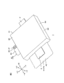
- FIG. 2 is a perspective view of the semiconductor power module 1 of FIG. 1 as viewed from above.
- FIG. 3 is a perspective view of the semiconductor power module 1 of FIG. 2 as viewed from below.
- the semiconductor power module 1 includes a rectangular parallelepiped package body 31.
- the package main body 31 includes an upper surface 32 having a rectangular shape in plan view, a lower surface 33 having the same shape as the upper surface 32, and four side surfaces 34 connecting the upper surface 32 and the lower surface 33.
- the + X direction and the ⁇ X direction, the + Y direction and the ⁇ Y direction, the + Z direction and the ⁇ Z direction shown in FIGS. 2 and 3 may be used.
- the + X direction and the ⁇ X direction are two directions along one side of the package body 31, and are simply referred to as “X direction” when collectively referred to.
- the + Y direction and the ⁇ Y direction are two directions along one other side orthogonal to the one side of the package main body 31, and are simply referred to as “Y direction” when collectively referred to.
- the + Z direction and the ⁇ Z direction are two directions along the thickness direction of the package main body 31, and are simply referred to as “Z direction” when collectively referred to.
- the X direction and the Y direction are two horizontal directions along two horizontal straight lines (X axis and Y axis) orthogonal to each other, and the Z direction is a vertical straight line (Z axis). It becomes the vertical direction along.
- the package body 31 is made of a resin material (thermosetting resin material) such as an epoxy resin, for example, and seals the plurality of first switching elements 5, the plurality of second switching elements 6, and the like.
- the output side terminal 2 is exposed on the side surface 34 on the + X direction side along the + X direction.
- the output side terminal 2 is drawn out in a square shape in plan view from the inside to the outside of the package main body 31.
- the high voltage side terminal 3 and the low voltage side terminal 4 are exposed along the ⁇ X direction on the side surface 34 on the ⁇ X direction side, which is the direction opposite to the exposure direction of the output side terminal 2. . That is, the output side terminal 2, the high voltage side terminal 3, and the low voltage side terminal 4 are arranged at positions facing each other with the package main body 31 interposed therebetween.
- the high-voltage side terminal 3 and the low-voltage side terminal 4 are respectively joined to a part of the insulating substrate 41 described later (the first extending portion 74 of the insulating substrate 41).
- the high-voltage side terminal 3 and the low-voltage side terminal 4 are drawn out together with a part of the insulating substrate 41 from the inside to the outside of the package main body 31 in a square shape in plan view.
- the low voltage side terminal 4 is bonded to the surface on the + Z direction side of the insulating substrate 41 (hereinafter simply referred to as “surface 42 of the insulating substrate 41”).
- the high-voltage side terminal 3 is bonded to the surface of the insulating substrate 41 on the ⁇ Z direction side (hereinafter simply referred to as “the back surface 43 of the insulating substrate 41”).
- the side surface on the + Y direction side which is a direction different from the exposure direction (+ X direction) of the output side terminal 2 and the exposure direction ( ⁇ X direction) of the high voltage side terminal 3 and the low voltage side terminal 4 34, the first gate terminal 14 and the first source sense terminal 15 described above, and the second gate terminal 20 and the second source sense terminal 21 described above are exposed along the + Y direction.
- the first gate terminal 14, the first source sense terminal 15, the second gate terminal 20, and the second source sense terminal 21 are respectively joined to a part of the insulating substrate 41 (second extending portion 75 of the insulating substrate 41) described later. Has been.
- the first gate terminal 14, the first source sense terminal 15, the second gate terminal 20, and the second source sense terminal 21 together with a part of the insulating substrate 41 (second extending portion 75 of the insulating substrate 41), the package body 31. Is drawn out from the inside to the outside in a plan view band shape (rectangular view in plan view).
- the second gate terminal 20 and the second source sense terminal 21 are bonded to the surface 42 of the insulating substrate 41 as shown in FIG.
- the first gate terminal 14 and the first source sense terminal 15 are bonded to the back surface 43 of the insulating substrate 41 as shown in FIG.
- the heat radiating member 35 is exposed on the lower surface 33 of the package main body 31.
- the heat radiating member 35 dissipates heat generated by the plurality of first switching elements 5 and the plurality of second switching elements 6 to the outside.
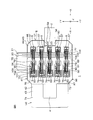
- FIG. 4 is an exploded perspective view showing the internal structure of the semiconductor power module 1 of FIG.
- FIG. 5 is a plan view showing the internal structure of the semiconductor power module 1 of FIG.
- FIG. 6 is a side view showing the internal structure of the semiconductor power module 1 of FIG.
- FIG. 7 is an enlarged view of region VII in FIG. 8 is a cross-sectional view taken along line VIII-VIII in FIG.
- the semiconductor power module 1 includes an insulating substrate 41.
- the insulating substrate 41 has a front surface 42 and a back surface 43. On the surface 42 side of the insulating substrate 41, the low voltage side terminal 4 is arranged.
- the output side terminal 2 is disposed on the back surface 43 side of the insulating substrate 41.
- the high voltage side terminal 3 is arranged on the back surface 43 side of the insulating substrate 41.
- a plurality of first switching elements 5 electrically connected to the output side terminal 2 and the high voltage side terminal 3, and the output side terminal 2 and the low voltage side terminal 4 are electrically connected to the back surface 43 side of the insulating substrate 41.
- a plurality of connected second switching elements 6 are arranged.
- the semiconductor power module 1 has a structure in which the high voltage side terminal 3 and the low voltage side terminal 4 face each other with the insulating substrate 41 interposed therebetween.
- the high-voltage side terminal 3 and the low-voltage side terminal 4 and their peripheral structures will be specifically described.
- the semiconductor power module 1 includes a first unit U1 including a plurality of first switching elements 5, a plurality of second switching elements 6 and an output side terminal 2, an insulating substrate 41, A second unit U2 including a high-voltage side terminal 3 and a low-voltage side terminal 4, and the second unit U2 is stacked on the first unit U1.
- the first unit U1 is disposed on the support substrate 44 having a square shape in plan view, the first conductor pattern 45 formed on the support substrate 44, and the first conductor pattern 45.
- the support substrate 44 includes a surface in the + Z direction (hereinafter simply referred to as “surface 46 of the support substrate 44”) and a surface in the ⁇ Z direction (hereinafter simply referred to as “back surface 47 of the support substrate 44”).
- the support substrate 44 is disposed on the back surface 43 side of the insulating substrate 41 at a distance from the insulating substrate 41, and supports the first switching element 5 and the second switching element 6 on the front surface 46 side.
- the support substrate 44 has a thickness of 5 mm or less, for example.
- the support substrate 44 may have a thickness of 0.3 mm to 0.7 mm.
- the support substrate 44 may be an inorganic insulating substrate such as ceramic (for example, AlN, SiN, SiO 2 ), or may be an organic insulating substrate such as a resin (for example, epoxy resin).
- the first conductor pattern 45 is a conductor film made of, for example, copper (Cu), and is directly bonded to the surface 46 of the support substrate 44.
- the first conductor pattern 45 electrically connects the first high voltage side conductor pattern 48 that electrically connects the high voltage side terminal 3 and the first switching element 5, and the output side terminal 2 and the second switching element 6. And a first output-side conductor pattern 49 connected to the.
- the first high-voltage side conductor pattern 48 is disposed at the end of the support substrate 44 on the ⁇ X direction side, and is formed in a square shape in plan view extending along the Y direction.
- the first output-side conductor pattern 49 is disposed at the end of the support substrate 44 on the + X direction side, and is formed in a square shape in plan view extending along the Y direction.
- the width of the first output side conductor pattern 49 in the X direction is set to a value larger than the width of the first high voltage side conductor pattern 48 in the X direction.
- a plurality of first switching elements 5 are joined on the first high-voltage side conductor pattern 48.
- the plurality of first switching elements 5 are arranged in a line along the Y direction.
- each first switching element 5 includes a first element surface 50 in the + Z direction where the first source electrode 10 and the first gate electrode 12 are disposed, and a first drain electrode 11.
- This is a so-called vertical MISFET provided with a first element body 52 having a first element back surface 51 in the ⁇ Z direction.
- the first element body 52 includes a Si substrate, a SiC substrate, or a wide band gap type semiconductor substrate.
- first source electrodes 10 and one first gate electrode 12 are formed on the first element surface 50.
- Each first switching element 5 is joined to the first high-voltage side conductor pattern 48 with the first element back surface 51 of the first element body 52 facing the front surface 46 of the support substrate 44.
- Each first switching element 5 is joined to the first high voltage side conductor pattern 48 by joining the first drain electrode 11 and the first high voltage side conductor pattern 48 via the first conductive bonding material 53.
- the first conductive bonding material 53 may be solder.
- a plurality of second switching elements 6 are joined on the first output-side conductor pattern 49.
- the plurality of second switching elements 6 are arranged in a line along the Y direction and arranged to face each first switching element 5 in a one-to-one correspondence in the X direction.
- each second switching element 6 has a second element surface 54 in the + Z direction where second source electrode 16 and second gate electrode 18 are arranged, and second drain electrode 17 is arranged.
- This is a so-called vertical MISFET provided with a second element body 56 having a second element back surface 55 in the ⁇ Z direction.
- the second element body 56 includes a Si substrate, a SiC substrate, or a wide band gap type semiconductor substrate.
- each second switching element 6 is joined to the first output side conductor pattern 49 in a state where the second element back surface 55 of the second element body 56 is opposed to the surface 46 of the support substrate 44.
- Each second switching element 6 is joined to the first output-side conductor pattern 49 by joining the second drain electrode 17 and the first output-side conductor pattern 49 via the second conductive joining material 57. Yes.
- the second conductive bonding material 57 may be solder.
- the output-side terminal 2 is disposed on the end side in the + X direction of the support substrate 44 with a space from each second switching element 6, and the first output-side conductor pattern 49. Are joined to the central portion in the longitudinal direction.
- the output side terminal 2 has a thickness larger than the thickness of the high voltage side terminal 3 or the thickness of the low voltage side terminal 4. As described above, the output side terminal 2 is electrically connected to the first switching element 5 and the second switching element 6 in common.
- the output side terminal 2 has a thickness at least equal to or greater than the total value of the thickness of the high voltage side terminal 3 and the thickness of the low voltage side terminal 4 from the viewpoint of suppressing an increase in resistance value. preferable.
- the output side terminal 2 is formed in a plate shape or block shape having a rectangular shape in plan view extending in the X direction, and has a plurality of notches 59 at the end portion 58 on the ⁇ X direction side. .
- the plurality of notches 59 are each formed in a groove shape extending along the same direction (X direction).
- the end portion 58 of the output side terminal 2 is joined to the first output side conductor pattern 49 via the third conductive joining material 60.
- the third conductive bonding material 60 may be solder.
- the third conductive bonding material 60 includes a plurality of pieces formed on the end portion 58. In the notch 59.
- the first unit U1 further includes the above-described heat radiating member 35 disposed on the back surface 47 side of the support substrate 44.
- the heat dissipating member 35 is formed by a rectangular conductive film made of copper (Cu) bonded directly to the back surface 47 of the support substrate 44. Covers almost the entire area.
- the heat generated from the plurality of first switching elements 5 and the plurality of second switching elements 6 is transmitted to the heat radiating member 35 via the first conductor pattern 45 and the support substrate 44, and is dissipated to the outside.
- the second unit U2 is disposed on the insulating substrate 41, the second conductor pattern 71 disposed on the back surface 43 side of the insulating substrate 41, and the front surface 42 side of the insulating substrate 41.
- Third conductor pattern 72 formed.
- the insulating substrate 41 has a thickness of 5 mm or less, for example.
- the insulating substrate 41 may have a thickness of 0.3 mm or greater and 0.7 mm or less.
- the insulating substrate 41 may be an inorganic insulating substrate such as ceramic (for example, AlN, SiN, SiO 2 ), or may be an organic insulating substrate such as a resin (for example, epoxy resin).
- the insulating substrate 41 includes a main body 73 having a rectangular shape in plan view that faces the surface 46 of the support substrate 44 in a plan view, and an outside of the support substrate 44 along the ⁇ X direction from the ⁇ X direction end of the main body 73.
- a first extending portion 74 extending in the region, and a second extending portion 75 extending from the end portion of the main body portion 73 in the + Y direction to the region outside the support substrate 44 along the + Y direction.
- the insulating substrate 41 is formed in an L shape in plan view by the main body portion 73, the first extending portion 74 and the second extending portion 75.
- the main body 73 of the insulating substrate 41 is disposed so as to face the first high voltage side conductor pattern 48 and the first output side conductor pattern 49.
- the main body 73 of the insulating substrate 41 includes a plurality (five in this embodiment) of first removal regions 76 that expose the first element surfaces 50 of the first switching elements 5 in plan view, and the second switching elements 6. And a plurality of (in this embodiment, five) third removal regions 78 that selectively expose the ⁇ X-direction end of the first output-side conductor pattern 49.
- the first removal region 76, the second removal region 77, and the third removal region 78 are regions formed by selectively removing a part of the insulating substrate 41, and are disposed on the ⁇ Z direction side of the insulating substrate 41. Each member is exposed.
- the first removal region 76, the second removal region 77, and the third removal region 78 each include an opening and / or a notch.
- each of the first removal regions 76 is made of a square-shaped opening that exposes each of the first switching elements 5 in a one-to-one correspondence, and is equally spaced in a line along the Y direction. It is formed so that it may line up with.
- Each first removal region 76 may be a rectangular cutout portion in plan view that exposes each first switching element 5 one by one in a one-to-one correspondence instead of the opening.
- two or more first switching elements 5 or all of the first switching elements 5 are opened and / or notched in a square shape in plan view extending in the Y direction so as to be exposed collectively.
- a plurality of or one first removal region 76 may be formed.
- the second removal region 77 is formed by the peripheral edge on the + X direction side of the insulating substrate 41, and in addition to the plurality of second switching elements 6, the second output region 77 on the + X direction side of the first output-side conductor pattern 49. The end is also exposed.
- an opening having a rectangular shape in plan view that exposes each second switching element 6 one by one in a one-to-one correspondence relationship and / or A plurality of second removal regions 77 made of notches and aligned in a line along the Y direction may be formed.
- two or more second switching elements 6 or all or all of the second switching elements 6 are made of a plurality of or one of the first and second openings composed of square-shaped openings and / or notches extending in the Y direction so as to be exposed at once. 2
- the removal area 77 may be formed.
- the plurality of third removal regions 78 are aligned in a line along the Y direction and are formed to face the plurality of first removal regions 76 in a one-to-one correspondence relationship in the X direction.
- Plural or one third removal consisting of two or more first switching elements 5 or all of the first switching elements 5 in the X direction and having a quadrangular opening and / or cutout in plan view extending in the Y direction.
- a region 78 may be formed.
- the first extending portion 74 of the insulating substrate 41 is a portion that does not face the support substrate 44 in plan view, and is formed in a square shape in plan view in this embodiment.
- the width of the first extending portion 74 of the insulating substrate 41 in the Y direction is set to a value smaller than the width of the main body portion 73 in the Y direction.
- the second extending portion 75 of the insulating substrate 41 is a portion that does not face the support substrate 44 in a plan view, and is formed in a square shape in a plan view in this embodiment.
- the width of the second extending portion 75 of the insulating substrate 41 in the X direction is set to a value smaller than the width of the main body portion 73 in the X direction.
- the second conductor pattern 71 disposed on the back surface 43 side of the insulating substrate 41 is a conductor film made of, for example, copper (Cu), and is directly bonded to the back surface 43 of the insulating substrate 41.
- the second conductor pattern 71 is joined to the high voltage side terminal 3 joined to the first extending portion 74 of the insulating substrate 41 and the main body portion 73 of the insulating substrate 41, and is connected to the high voltage side terminal 3 and the first high voltage side.
- a second high-voltage side conductor pattern 79 electrically connected to the conductor pattern 48 (first switching element 5), and a second output-side conductor pattern 80 electrically connected to the first output-side conductor pattern 49; are integrally included.
- the high voltage side terminal 3 is disposed at a position spaced inward from the periphery of the first extending portion 74 in the first extending portion 74 of the insulating substrate 41, and is formed in a square shape in plan view. Yes.
- the peripheral edge of the high voltage side terminal 3 is arranged at a position at least 2 mm away from the peripheral edge of the first extending portion 74 of the insulating substrate 41, whereby the peripheral edge of the high voltage side terminal 3 and the first edge of the insulating substrate 41 are arranged.
- An insulating region is set between the peripheral edge of the one extending portion 74.
- the second high voltage side conductor pattern 79 includes a first high voltage side portion 81 that is joined to the end portion of the main body 73 on the ⁇ X direction side and connected to the high voltage side terminal 3.
- the first high voltage side portion 81 is electrically connected to the first high voltage side conductor pattern 48 via the fourth conductive bonding material 83.
- the second high-voltage side conductor pattern 79 is a comb-like second high-voltage side portion drawn out from the first high-voltage side portion 81 toward the side of each first switching element 5 (first removal region 76). 82.
- the second output-side conductor pattern 80 is disposed at the end on the + X direction side of the insulating substrate 41 and is formed in a square shape in plan view extending in the Y direction.
- the second output-side conductor pattern 80 is connected to the first output-side conductor pattern 49 via the fifth conductive bonding material 85 in the region between the end portion on the ⁇ X direction side of the first output-side conductor pattern 49 and the second switching element 6.
- the side conductor pattern 49 is electrically connected.
- the plurality of second output-side conductor patterns 80 selectively expose the first output-side conductor patterns 49 at positions corresponding to the plurality of third removal regions 78 of the insulating substrate 41 (five in this embodiment).
- the fourth removal region 84 is provided.
- the end on the ⁇ X direction side of the second output side conductor pattern 80 is formed in a comb shape by the plurality of fourth removal regions 84.
- the fourth removal region 84 may be an opening and / or a notch that is rectangular in plan view and extends in the Y direction.
- the end of the first output side conductor pattern 49 on the ⁇ X direction side is selectively exposed by the third removal region 78 of the insulating substrate 41 and the fourth removal region 84 of the second output side conductor pattern 80.
- the third conductor pattern 72 disposed on the surface 42 side of the insulating substrate 41 is a conductor film made of, for example, copper (Cu), and is directly bonded to the surface 42 of the insulating substrate 41.
- the third conductor pattern 72 is joined to the low voltage side terminal 4 joined to the second extending portion 75 of the insulating substrate 41 and the main body portion 73 of the insulating substrate 41 and is electrically connected to the low voltage side terminal 4. And a low-voltage side conductor pattern 86.
- the low voltage side terminal 4 is disposed at a position spaced inward from the periphery of the first extending portion 74 in the first extending portion 74 of the insulating substrate 41, and is formed in a square shape in plan view. Yes.
- the low voltage side terminal 4 is opposed to the high voltage side terminal 3 with the first extending portion 74 of the insulating substrate 41 interposed therebetween.
- the low voltage side terminal 4 is formed in a square shape in plan view having the same area and the same shape as the high voltage side terminal 3, and the entirety of the low voltage side terminal 4 includes the first extending portion 74 of the insulating substrate 41. It faces the high-voltage side terminal 3 with being sandwiched.
- the peripheral edge of the low voltage side terminal 4 is disposed at a position at least 2 mm away from the peripheral edge of the first extending portion 74 of the insulating substrate 41, whereby the peripheral edge of the low voltage side terminal 4 and the first edge of the insulating substrate 41 are arranged.
- An insulating region is set between the peripheral edge of the one extending portion 74.
- the low voltage side conductor pattern 86 is joined to the end portion of the main body portion 73 on the ⁇ X direction side and connected to the low voltage side terminal 4, and the + X direction side of the main body portion 73 on the + X direction side.
- a second low-voltage side portion 88 joined to the end portion and a third low-voltage side portion 89 connecting them are included.
- the third low voltage side portion 89 connects the first low voltage side portion 87 and the second low voltage side portion 88 so as to avoid the plurality of first removal regions 76 and the plurality of third removal regions 78.
- the side conductor pattern 86 is opposed to the second high voltage side conductor pattern 79 with the main body 73 of the insulating substrate 41 interposed therebetween. More specifically, the first low voltage side portion 87 of the low voltage side conductor pattern 86 is opposed to the first high voltage side portion 81 of the second high voltage side conductor pattern 79 with the main body portion 73 of the insulating substrate 41 interposed therebetween. is doing.
- the third low voltage side portion 89 of the low voltage side conductor pattern 86 faces the second high voltage side portion 82 of the second high voltage side conductor pattern 79 with the main body 73 of the insulating substrate 41 interposed therebetween.
- the second conductor pattern 71 disposed on the back surface 43 side of the insulating substrate 41 includes the first gate terminal 14 on the high voltage side and the first source sense terminal 15 on the high voltage side. And further including.
- the first gate terminal 14 and the first source sense terminal 15 are arranged adjacent to each other between the second high voltage side conductor pattern 79 and the second output side conductor pattern 80.
- the first gate terminal 14 is disposed on the ⁇ X direction side
- the first source sense terminal 15 is disposed on the + X direction side.
- the first gate terminal 14 and the first source sense terminal 15 are each formed in a plan view band shape (rectangular view plan view) extending along the Y direction, and the second extending portion 75 from the main body portion 73 of the insulating substrate 41. Has been drawn to.
- each portion drawn out to the second extending portion 75 of the insulating substrate 41 is located at a position spaced inward from the periphery of the second extending portion 75. Each is arranged.
- first contact holes 92 for selectively exposing the first gate terminals 14 and the first source sense terminals 15 are selectively exposed.
- a plurality (five in this embodiment) of second contact holes 93 are selectively formed.
- a plurality of first contact holes 92 are provided in each region between the first removal region 76 and the third removal region 78.
- the plurality of second contact holes 93 are provided one by one so as to be adjacent to the first contact hole 92 in each region between the first removal region 76 and the third removal region 78.
- the third conductor pattern 72 arranged on the surface 42 side of the insulating substrate 41 includes a plurality of (five in the present embodiment) gate pads 94 connected to the first gate terminal 14 via the first contact holes 92. And a plurality (five in this embodiment) of source sense pads 95 connected to the first source sense terminals 15 through the respective second contact holes 93.
- the third conductor pattern 72 includes the second gate terminal 20 on the low voltage side and the second source sense terminal 21 on the low voltage side.
- the second gate terminal 20 and the second source sense terminal 21 are connected to the + X direction end of the insulating substrate 41 (the peripheral edge of the insulating substrate 41 on the + X direction side and the second low voltage side portion 88 of the low voltage side conductor pattern 86. Between the two areas).
- the second gate terminal 20 is disposed on the ⁇ X direction side
- the second source sense terminal 21 is disposed on the + X direction side.
- the second gate terminal 20 and the second source sense terminal 21 are formed in a plan view band shape (a rectangular shape in plan view) extending along the Y direction, and extend from the main body portion 73 of the insulating substrate 41 to the second extension portion 75. Each is pulled out.
- each part drawn out to the second extending portion 75 of the insulating substrate 41 is located at a position spaced inward from the periphery of the second extending portion 75. Each is arranged.
- the second gate terminal 20 and the second source sense terminal 21 are joined to a position not overlapping the first gate terminal 14 and the first source sense terminal 15 in plan view (FIGS. 2 and 3). See also).
- the first conductor pattern 45 disposed on the front surface 46 side of the support substrate 44 includes a dummy gate terminal 96 provided corresponding to the first gate terminal 14 and a dummy provided corresponding to the first source sense terminal 15. Source sense terminal 97.
- the dummy gate terminal 96 and the dummy source sense terminal 97 are disposed between the first high voltage side conductor pattern 48 and the first output side conductor pattern 49, and the entirety thereof is located on the surface 46 of the support substrate 44. ing.
- the first source electrode 10 of each first switching element 5 is bonded to the surface 46 of the support substrate 44 through the first bonding wire 101 as a connection member.
- the first output side conductor pattern 49 is electrically connected.
- the first bonding wire 101 is disposed on the surface 42 side of the insulating substrate 41, and the first removal region 76 and the third removal region 78 of the insulating substrate 41 (the fourth removal region 84 of the second output-side conductor pattern 80).
- the first source electrode 10 of each first switching element 5 and the first output-side conductor pattern 49 are connected via each other.
- the first source electrode 10 is electrically connected to the output-side terminal 2 via the first bonding wire 101 and the first output-side conductor pattern 49.
- each first switching element 5 the first drain electrode 11 is electrically connected to the high voltage side terminal 3 via the first high voltage side conductor pattern 48 and the second high voltage side conductor pattern 79. In this way, each first switching element 5 is electrically connected between the output side terminal 2 and the high voltage side terminal 3.
- the first gate electrode 12 of each first switching element 5 is electrically connected to the gate pad 94 via a second bonding wire 102 as a connecting member. Thereby, the first gate electrode 12 and the first gate terminal 14 of each first switching element 5 are electrically connected.
- At least one first source electrode 10 of each first switching element 5 is electrically connected to a source sense pad 95 via a third bonding wire 103 as a connection member. As a result, at least one first source electrode 10 of each first switching element 5 and the first source sense terminal 15 are electrically connected.
- the second source electrode 16 of each second switching element 6 has a low voltage side conductor pattern 86 (low voltage side conductor) bonded to the surface 42 of the insulating substrate 41 via a fourth bonding wire 104 as a connecting member.
- the second low voltage side portion 88) of the pattern 86 is electrically connected.
- the fourth bonding wire 104 is disposed on the surface 42 side of the insulating substrate 41, and the second source electrode 16 and the low voltage side conductor pattern of each second switching element 6 through the second removal region 77 of the insulating substrate 41. 86 is connected.
- the second source electrode 16 is electrically connected to the low voltage side terminal 4 via the fourth bonding wire 104 and the low voltage side conductor pattern 86.
- each second switching element 6 the second drain electrode 17 is electrically connected to the output-side terminal 2 via the first output-side conductor pattern 49. In this way, each second switching element 6 is electrically connected between the output side terminal 2 and the low voltage side terminal 4.
- the second gate electrode 18 of each second switching element 6 is electrically connected to the second gate terminal 20 via a fifth bonding wire 105 as a connection member.
- the fifth bonding wire 105 is disposed on the surface 42 side of the insulating substrate 41, and the second gate electrode 18 and the second gate terminal 20 of each second switching element 6 through the second removal region 77 of the insulating substrate 41. And connected.
- At least one second source electrode 16 of each second switching element 6 is electrically connected to the second source sense terminal 21 via a sixth bonding wire 106 as a connection member.
- the sixth bonding wire 106 is disposed on the surface 42 side of the insulating substrate 41, and is connected to at least one second source electrode 16 of each second switching element 6 and the second through the second removal region 77 of the insulating substrate 41.
- the source sense terminal 21 is connected.
- the package body 31 includes a part of the output side terminal 2, a part of the high voltage side terminal 3, a part of the low voltage side terminal 4, a part of the first gate terminal 14, and a part of the first source sense terminal 15.
- the insulating substrate 41 and the support substrate 44 are sealed so that a part of the second gate terminal 20, a part of the second source sense terminal 21, and the heat dissipation member 35 are selectively exposed.
- a part of the high-voltage side terminal 3 and a part of the low-voltage side terminal 4 are drawn to the outside of the package main body 31 together with the first extending portion 74 of the insulating substrate 41.
- a part of the first gate terminal 14, a part of the first source sense terminal 15, a part of the second gate terminal 20 and a part of the second source sense terminal 21 are together with the second extending portion 75 of the insulating substrate 41. It is pulled out of the package body 31.
- the package main body 31 may be formed by a transfer molding method or may be formed by a compression molding method.
- a package body 31 that selectively seals the insulating substrate 41 and the like is formed by pouring resin into a mold having a cavity having a predetermined shape in which the insulating substrate 41 and the like are accommodated.
- the insulating substrate 41 or the like means the internal structure of the semiconductor power module 1 excluding the package main body 31 (the same applies hereinafter).
- the insulating substrate 41 or the like is immersed in the resin, or the insulating substrate 41 is embedded in a mold having a cavity having a predetermined shape. Etc. are accommodated and arranged, and a resin is immersed in the mold to form a package body 31 for selectively sealing the insulating substrate 41 and the like.
- the package main body 31 may include a resin casing (resin case) having an internal space, and the insulating substrate 41 and the like may be accommodated in the internal space of the casing.
- the output side terminal 2, the high voltage side terminal 3, the low voltage side terminal 4, and the plurality of first switching elements connected to the output side terminal 2 and the high voltage side terminal 3. 5 and a plurality of second switching elements 6 connected to the output side terminal 2 and the low voltage side terminal 4 constitute one half bridge circuit 7.
- the plurality of first switching elements 5 constitutes an upper arm 8 on the high voltage side
- the plurality of second switching elements 6 constitutes a lower arm 9 on the low voltage side.
- a current path from the high voltage side terminal 3 to the output side terminal 2 through each first switching element 5 is formed on the back surface 43 side of the insulating substrate 41, and each second path from the output side terminal 2 to each second side.
- a current path toward the low voltage side terminal 4 through the switching element 6 is formed on the surface 42 side of the insulating substrate 41.
- the direction of the current flowing through the high voltage side terminal 3 and the direction of the current flowing through the low voltage side terminal 4 are opposite to each other with the insulating substrate 41 interposed therebetween.
- the distance between the high voltage side terminal 3 and the low voltage side terminal 4 is based on the thickness of the insulating substrate 41 (5 mm or less in this embodiment) on which the high voltage side terminal 3 and the low voltage side terminal 4 are opposed to each other. Therefore, the high-voltage side terminal 3 and the low-voltage side terminal 4 can be satisfactorily arranged close to each other while maintaining insulation.
- the magnetic field generated at the high voltage side terminal 3 and the magnetic field generated at the low voltage side terminal 4 can be satisfactorily offset, so that the mutual inductance component between the high voltage side terminal 3 and the low voltage side terminal 4 is improved. Can be reduced. Therefore, the semiconductor power module 1 which can reduce an inductance component favorably can be provided.
- the insulating substrate 41 includes a first removal region 76 that exposes the first switching element 5 and a second removal region 77 that exposes the second switching element 6 in plan view.
- a first removal region 76 that exposes the first switching element 5
- a second removal region 77 that exposes the second switching element 6 in plan view.
- the heat generated in the first switching element 5 can be dissipated from the back surface 43 side to the front surface 42 side of the insulating substrate 41 through the first removal region 76, and the heat generated in the second switching element 6 can be dissipated. 2 It is possible to diffuse the insulating substrate 41 from the back surface 43 side to the front surface 42 side through the removal region 77.
- the temperature rise of the 1st switching element 5 and the 2nd switching element 6 can be suppressed favorably.
- the first removal region 76 and the second removal region 77 are provided on the insulation substrate 41.
- the heat dissipation member 35 is provided on the back surface 47 side of the support substrate 44. Therefore, the heat generated in the first switching element 5 and the heat generated in the second switching element 6 can be well dissipated to the outside through the support substrate 44 and the heat radiating member 35. Therefore, the semiconductor power module 1 that can effectively suppress the temperature rise of the first switching element 5 and the second switching element 6 can be provided.
- one half bridge circuit 7 is configured by the plurality of first switching elements 5 and the plurality of second switching elements 6 has been described.
- the number of the first switching elements 5 and the number of the second switching elements 6 are not limited to this.
- one half-bridge circuit 7 may be configured by one first switching element 5 and one second switching element 6.
- One half-bridge circuit 7 may be configured by two or more first switching elements 5 and two or more second switching elements 6.
- FIG. 9 is an electric circuit diagram showing an electrical structure according to a first modification of the semiconductor power module 1 of FIG.
- the same reference numerals are assigned to the configurations shown in FIG.
- IGBT Insulated Gate Bipolar Transistor
- the half bridge circuit 7 is constituted by an IGBT.
- the first switching element 5 and the second switching element 6 may include an IGBT formed on a Si substrate, a SiC substrate, or a wide band gap type semiconductor substrate.
- the first switching element 5 includes a first emitter electrode 110 instead of the first source electrode 10 described above, and includes a first collector electrode 111 instead of the first drain electrode 11 described above.
- a first gate electrode 112 is provided instead of the gate electrode 12.
- the first emitter electrode 110 and the first collector electrode 111 constitute a pair of first main electrodes, and the first gate electrode 112 has a current flowing between the pair of first main electrodes.
- the 1st control electrode which controls is constituted.
- the second switching element 6 includes a second emitter electrode 113 instead of the second source electrode 16 described above, a second collector electrode 114 instead of the second drain electrode 17 described above, and the second gate electrode 18 described above. Instead, a second gate electrode 115 is provided.
- each second switching element 6 the second emitter electrode 113 and the second collector electrode 114 constitute a pair of first main electrodes, and the second gate electrode 115 is a current flowing between the pair of first main electrodes.
- the 1st control electrode which controls is constituted.
- the first gate electrode 112 is electrically connected to the first gate terminal 116 instead of the first gate terminal 14, and the first emitter electrode 110 is connected to the first source sense terminal 15. Instead, it is electrically connected to the first emitter sense terminal 117.
- the second gate electrode 115 is electrically connected to the second gate terminal 118 instead of the second gate terminal 20, and the second emitter electrode 113 is replaced by the second emitter sense terminal instead of the second source sense terminal 21. 119 is electrically connected. Even with such a configuration, the same effects as those described in the above-described embodiment can be obtained.
- FIG. 10 is an electric circuit diagram showing an electrical structure according to a second modification of the semiconductor power module 1 of FIG.
- the same reference numerals are assigned to the configurations shown in FIG.
- BJT Bipolar Junction Transistor
- the half bridge circuit 7 is configured by BJT.
- the first switching element 5 and the second switching element 6 may include BJT formed on a Si substrate, a SiC substrate, or a wide band gap type semiconductor substrate.
- the first switching element 5 includes a first emitter electrode 120 instead of the first source electrode 10 described above, and includes a first collector electrode 121 instead of the first drain electrode 11 described above.
- a first base electrode 122 is provided instead of the gate electrode 12.
- the first emitter electrode 120 and the first collector electrode 121 constitute a pair of first main electrodes, and the first base electrode 122 has a current flowing between the pair of first main electrodes.
- the 1st control electrode which controls is constituted.
- the second switching element 6 includes a second emitter electrode 123 instead of the above-described second source electrode 16, a second collector electrode 124 instead of the above-described second drain electrode 17, and the above-described second gate electrode 18. Instead, a second base electrode 125 is provided.
- each second switching element 6 the second emitter electrode 123 and the second collector electrode 124 constitute a pair of first main electrodes, and the second base electrode 125 is a current flowing between the pair of first main electrodes.
- the 1st control electrode which controls is constituted.
- the first base electrode 122 is electrically connected to the first base terminal 126 instead of the first gate terminal 14, and the first emitter electrode 120 is connected to the first source sense terminal 15. Instead, it is electrically connected to the first emitter sense terminal 127.
- the second base electrode 125 is electrically connected to the second base terminal 128 instead of the second gate terminal 20, and the second emitter electrode 123 is replaced with the second source sense terminal 21 and the second emitter sense terminal. 129 is electrically connected. Even with such a configuration, the same effects as those described in the above-described embodiment can be obtained.
- the MISFET, IGBT, and BJT described above are preferably formed on a SiC substrate or a wide band gap semiconductor substrate among the Si substrate, SiC substrate, or wide band gap semiconductor substrate described above.
- a supplementary explanation of the wide band gap type semiconductor substrate will be given below.
- Examples of the semiconductor material of the wide band gap semiconductor substrate include a III-V group semiconductor containing a group III element and a group V element, a nitride semiconductor (eg, gallium nitride), diamond, and the like.
- the aforementioned SiC substrate is also an example of a wide band gap type semiconductor substrate.
Landscapes
- Engineering & Computer Science (AREA)
- Power Engineering (AREA)
- Inverter Devices (AREA)
- Chemical & Material Sciences (AREA)
- Materials Engineering (AREA)
- Dot-Matrix Printers And Others (AREA)
- Record Information Processing For Printing (AREA)
- Accessory Devices And Overall Control Thereof (AREA)
Abstract
半導体パワーモジュールは、一方表面および他方表面を有する絶縁基板と、前記絶縁基板の前記一方表面側に配置された出力側端子と、前記絶縁基板の前記一方表面側に配置された第1電源端子と、前記絶縁基板を挟んで前記第1電源端子に対向するように、前記絶縁基板の前記他方表面側に配置され、前記第1電源端子に印加される電圧とは異なる大きさの電圧が印加される第2電源端子と、前記絶縁基板の前記一方表面側に配置され、前記出力側端子および前記第1電源端子に電気的に接続された第1スイッチング素子と、前記絶縁基板の前記一方表面側に配置され、前記出力側端子および前記第2電源端子に電気的に接続された第2スイッチング素子とを含む。
Description
本発明は、半導体パワーモジュールに関する。
特許文献1には、複数のスイッチング素子を含む半導体パワーモジュールの一例として、インバータモジュールが開示されている。このインバータモジュールは、第1半導体素子(第1スイッチング素子)と、第2半導体素子(第2スイッチング素子)と、これらを収容する樹脂ケースとを備えている。
このインバータモジュールにおいて、樹脂ケースの一方側端部には、第1半導体素子に接続される正極側端子(電源端子)と、第2半導体素子に接続される負極側端子(電源端子)とが間隔を空けて配置されている。樹脂ケースの他方側端部には、第1半導体素子および第2半導体素子に共通に接続される一対の出力側端子が配置されている。
一般的に、複数のスイッチング素子を備えた半導体パワーモジュールでは、スイッチング動作時にサージ電圧が生じる虞があるという問題がある。サージ電圧の大きさは、電流が流れる配線等の電流経路のインダクタンス成分に比例するため、電流経路からインダクタンス成分を取り除くことが一つの課題となっている。
ところで、特許文献1に開示された半導体パワーモジュールでは、互いに異なる電圧が印加される2つの電源端子が、樹脂ケースの一方側端部において互いに間隔を空けて配置されている。
これら2つの電源端子間の距離は、樹脂ケースの形状に依存して設定されているため、比較的に大きい値となる。そのため、一方の電源端子で発生する磁界と、他方の電源端子で発生する磁界とを良好に相殺させることができないから、相互誘導効果に起因して端子間の相互インダクタンス成分が増加する虞がある。
そこで、本発明は、インダクタンス成分を低減できる半導体パワーモジュールを提供する。
本発明は、一方表面および他方表面を有する絶縁基板と、前記絶縁基板の前記一方表面側に配置された出力側端子と、前記絶縁基板の前記一方表面側に配置された第1電源端子と、前記絶縁基板を挟んで前記第1電源端子に対向するように、前記絶縁基板の前記他方表面側に配置され、前記第1電源端子に印加される電圧とは異なる大きさの電圧が印加される第2電源端子と、前記絶縁基板の前記一方表面側に配置され、前記出力側端子および前記第1電源端子に電気的に接続された第1スイッチング素子と、前記絶縁基板の前記一方表面側に配置され、前記出力側端子および前記第2電源端子に電気的に接続された第2スイッチング素子とを含む、半導体パワーモジュールを提供する。
この半導体パワーモジュールによれば、第1電源端子および第2電源端子が対向配置される絶縁基板の厚さに基づいて、第1電源端子および第2電源端子間の距離を設定できる。これにより、絶縁性を保ちつつ、第1電源端子および第2電源端子を近接配置できる。
したがって、第1電源端子で発生する磁界と、第2電源端子で発生する磁界とを良好に相殺できるから、第1電源端子および第2電源端子間の相互インダクタンス成分を低減できる。よって、インダクタンス成分を低減できる半導体パワーモジュールを提供できる。
本発明における上述の、またはさらに他の目的、特徴および効果は、添付図面を参照して次に述べる実施形態の説明により明らかにされる。
図1は、本発明の一実施形態に係る半導体パワーモジュール1の電気的構造を示す電気回路図である。
図1を参照して、本実施形態に係る半導体パワーモジュール1は、出力側端子2と、高電圧側端子3(第1電源端子)と、高電圧側端子3に印加される電圧よりも低い電圧が印加される低電圧側端子4(第2電源端子)とを含む。
半導体パワーモジュール1は、出力側端子2および高電圧側端子3間に接続された複数(本実施形態では5個)の第1スイッチング素子5と、出力側端子2および低電圧側端子4間に接続された複数(本実施形態では5個)の第2スイッチング素子6とを含む。
出力側端子2、高電圧側端子3、低電圧側端子4、複数の第1スイッチング素子5および複数の第2スイッチング素子6により、ハーフブリッジ回路7が構成されている。高電圧側端子3と低電圧側端子4とは、互いに近接配置されている。
ハーフブリッジ回路7において、複数の第1スイッチング素子5は、高電圧側の上アーム8を構成しており、複数の第2スイッチング素子6は、低電圧側の下アーム9を構成している。
各第1スイッチング素子5は、本実施形態では、Si基板、SiC基板またはワイドバンドギャップ型の半導体基板に形成されたMISFET(Metal Insulator Semiconductor Field Effect Transistor)を含み、第1ソース電極10、第1ドレイン電極11および第1ゲート電極12を有している。
各第1スイッチング素子5において、第1ソース電極10、第1ドレイン電極11は、一対の第1主電極を構成しており、第1ゲート電極12は、一対の第1主電極間を流れる電流を制御する第1制御電極を構成している。各第1スイッチング素子5は、第1ドレイン電極11および第1ソース電極10間に逆バイアス接続された第1ダイオード13を含む。
各第1スイッチング素子5は、第1ソース電極10が出力側端子2に電気的に接続され、第1ドレイン電極11が高電圧側端子3に電気的に接続されることによって、高電圧側端子3および低電圧側端子4間に接続されている。各第1スイッチング素子5の第1ゲート電極12は、高電圧側の第1ゲート端子14(第1制御端子)に共通に電気的に接続されている。
第1ゲート端子14は、各第1スイッチング素子5(各第1ゲート電極12)を駆動制御するための端子である。各第1スイッチング素子5の第1ソース電極10は、出力側端子2に加えて、高電圧側の第1ソースセンス端子15に共通に電気的に接続されている。第1ソースセンス端子15は、第1ソース電極10の電位を検出するための電位検出用の端子である。
各第2スイッチング素子6は、本実施形態では、Si基板、SiC基板またはワイドバンドギャップ型の半導体基板に形成されたMISFETを含み、第2ソース電極16、第2ドレイン電極17および第2ゲート電極18を有している。
各第2スイッチング素子6において、第2ソース電極16および第2ドレイン電極17は、一対の第2主電極を構成しており、第2ゲート電極18は、一対の第2主電極間を流れる電流を制御する第2制御電極を構成している。各第2スイッチング素子6は、第2ドレイン電極17および第2ソース電極16間に逆バイアス接続された第2ダイオード19を含む。
各第2スイッチング素子6は、第2ドレイン電極17が出力側端子2に電気的に接続され、第2ソース電極16が低電圧側端子4に電気的に接続されることによって、出力側端子2および低電圧側端子4間に接続されている。
出力側端子2は、第1スイッチング素子5の第1ソース電極10および第2スイッチング素子6の第2ドレイン電極17に共通に接続された共通端子でもある。各第2スイッチング素子6の第2ゲート電極18は、低電圧側の第2ゲート端子20(第1制御端子)に共通に電気的に接続されている。
第2ゲート端子20は、各第2スイッチング素子6(各第2ゲート電極18)を駆動制御するための端子である。各第2スイッチング素子6の第2ソース電極16は、低電圧側端子4に加えて、低電圧側の第2ソースセンス端子21に共通に電気的に接続されている。第2ソースセンス端子21は、第2ソース電極16の電位を検出するための電位検出用の端子である。
本実施形態に係る半導体パワーモジュール1は、たとえば、U相、V相およびW相を有する三相モータにおいて、U相、V相およびW相のいずれか一相を駆動させるためのインバータモジュールとして構成されている。したがって、U相、V相およびW相に対応する3個の半導体パワーモジュール1を備えることによって、三相モータを駆動するためのインバータ装置を提供できる。
インバータ装置では、各半導体パワーモジュール1の高電圧側端子3および低電圧側端子4間に直流電源が接続され、各半導体パワーモジュール1の出力側端子2に三相モータが負荷として接続される。高電圧側端子3および低電圧側端子4間には、低電圧側端子4側を基準電位として、たとえば500V以上2000V以下の直流電圧が印加される。
インバータ装置では、各半導体パワーモジュール1の第1スイッチング素子5および第2スイッチング素子6が、所定のスイッチングパターンで駆動制御される。これにより、直流電圧が三相交流電圧に変換され、三相モータに供給される。このようにして、三相モータが正弦波駆動される。
次に、図2および図3を参照して、半導体パワーモジュール1の外観について具体的に説明する。
図2は、図1の半導体パワーモジュール1を上側から見た斜視図である。図3は、図2の半導体パワーモジュール1を下側から見た斜視図である。
半導体パワーモジュール1は、直方体形状のパッケージ本体部31を含む。パッケージ本体部31は、平面視四角形状の上面32と、当該上面32と同一形状の下面33と、上面32および下面33を接続する4つの側面34とを含む。
以下では、説明の便宜上、図2および図3に示した+X方向および-X方向、+Y方向および-Y方向ならびに+Z方向および-Z方向を用いることがある。
+X方向および-X方向は、パッケージ本体部31の1辺に沿う2つの方向であり、これらを総称するときには単に「X方向」という。+Y方向および-Y方向はパッケージ本体部31の前記1辺と直交する他の1辺に沿う2つの方向であり、これらを総称するときには単に「Y方向」という。+Z方向および-Z方向はパッケージ本体部31の厚さ方向に沿う2つの方向であり、これらを総称するときには単に「Z方向」という。
パッケージ本体部31を水平面においたとき、X方向およびY方向は互いに直交する2つの水平な直線(X軸およびY軸)に沿う2つの水平方向となり、Z方向は鉛直な直線(Z軸)に沿う鉛直方向となる。
パッケージ本体部31は、たとえばエポキシ樹脂等の樹脂材料(熱硬化性の樹脂材料)からなり、複数の第1スイッチング素子5および複数の第2スイッチング素子6等を封止している。
パッケージ本体部31において、+X方向側の側面34には、当該+X方向に沿って前述の出力側端子2が露出している。出力側端子2は、本実施形態では、パッケージ本体部31の内側から外側に平面視四角形状に引き出されている。
出力側端子2の露出方向とは反対側の方向である-X方向側の側面34には、当該-X方向に沿って前述の高電圧側端子3および低電圧側端子4が露出している。つまり、出力側端子2と、高電圧側端子3および低電圧側端子4とは、パッケージ本体部31を挟んで互いに対向する位置に配置されている。
高電圧側端子3および低電圧側端子4は、後述する絶縁基板41の一部(絶縁基板41の第1延設部74)にそれぞれ接合されている。高電圧側端子3および低電圧側端子4は、絶縁基板41の一部と共にパッケージ本体部31の内側から外側に平面視四角形状に引き出されている。
低電圧側端子4は、図2に示されるように、絶縁基板41の+Z方向側の表面(以下、単に「絶縁基板41の表面42」という)に接合されている。高電圧側端子3は、図3に示されるように、絶縁基板41の-Z方向側の表面(以下、単に「絶縁基板41の裏面43」という)に接合されている。
パッケージ本体部31において、出力側端子2の露出方向(+X方向)、ならびに、高電圧側端子3および低電圧側端子4の露出方向(-X方向)とは異なる方向である+Y方向側の側面34には、前述の第1ゲート端子14および第1ソースセンス端子15と、前述の第2ゲート端子20および第2ソースセンス端子21とが、当該+Y方向に沿って露出している。
第1ゲート端子14、第1ソースセンス端子15、第2ゲート端子20および第2ソースセンス端子21は、後述する絶縁基板41の一部(絶縁基板41の第2延設部75)にそれぞれ接合されている。
第1ゲート端子14、第1ソースセンス端子15、第2ゲート端子20および第2ソースセンス端子21は、絶縁基板41の一部(絶縁基板41の第2延設部75)と共にパッケージ本体部31の内側から外側に平面視帯状(平面視長方形状)に引き出されている。
第2ゲート端子20および第2ソースセンス端子21は、図2に示されるように、絶縁基板41の表面42に接合されている。第1ゲート端子14および第1ソースセンス端子15は、図3に示されるように、絶縁基板41の裏面43に接合されている。
図3を参照して、パッケージ本体部31の下面33には、放熱部材35が露出している。この放熱部材35によって、複数の第1スイッチング素子5および複数の第2スイッチング素子6で生じた熱が外部に放散される。
次に、図4~図8を参照して、半導体パワーモジュール1の内部構造について具体的に説明する。
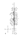
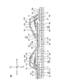
図4は、図1の半導体パワーモジュール1の内部構造を示す分解斜視図である。図5は、図1の半導体パワーモジュール1の内部構造を示す平面図である。図6は、図1の半導体パワーモジュール1の内部構造を示す側面図である。図7は、図6の領域VIIの拡大図である。図8は、図7のVIII-VIII線に沿う断面図である。
図4~図6を参照して、半導体パワーモジュール1は、絶縁基板41を含む。絶縁基板41は、表面42および裏面43を有している。絶縁基板41の表面42側には、低電圧側端子4が配置されている。絶縁基板41の裏面43側には、出力側端子2が配置されている。
絶縁基板41の裏面43側には、高電圧側端子3が配置されている。絶縁基板41の裏面43側には、出力側端子2および高電圧側端子3に電気的に接続された複数の第1スイッチング素子5と、出力側端子2および低電圧側端子4に電気的に接続された複数の第2スイッチング素子6とが配置されている。
半導体パワーモジュール1は、高電圧側端子3および低電圧側端子4が、絶縁基板41を挟んで互いに対向する構造を有している。以下、高電圧側端子3および低電圧側端子4、ならびに、それらの周辺の構造について具体的に説明する。
図4を参照して、本実施形態に係る半導体パワーモジュール1は、複数の第1スイッチング素子5、複数の第2スイッチング素子6および出力側端子2を含む第1ユニットU1と、絶縁基板41、高電圧側端子3および低電圧側端子4を含む第2ユニットU2とを備え、第1ユニットU1上に第2ユニットU2が積層配置された構成を有している。
図4~図6を参照して、第1ユニットU1は、平面視四角形状の支持基板44と、支持基板44上に形成された第1導体パターン45と、第1導体パターン45上に配置された複数の第1スイッチング素子5と、第1導体パターン45上に配置された複数の第2スイッチング素子6と、第1導体パターン45上に配置された出力側端子2とを含む。
支持基板44は、+Z方向の表面(以下、単に「支持基板44の表面46」という。)と、-Z方向の表面(以下、単に「支持基板44の裏面47」という。)とを含む。支持基板44は、絶縁基板41の裏面43側に当該絶縁基板41から間隔を空けて配置されており、その表面46側において第1スイッチング素子5および第2スイッチング素子6を支持している。
支持基板44は、たとえば5mm以下の厚さを有している。支持基板44は、0.3mm以上0.7mm以下の厚さを有していてもよい。支持基板44は、セラミック(たとえばAlN、SiN、SiO2)等の無機系の絶縁基板であってもよいし、樹脂(たとえばエポキシ樹脂)等の有機系の絶縁基板であってもよい。
第1導体パターン45は、たとえば銅(Cu)からなる導体膜であり、支持基板44の表面46に直接接合されている。第1導体パターン45には、高電圧側端子3と第1スイッチング素子5とを電気的に接続する第1高電圧側導体パターン48と、出力側端子2と第2スイッチング素子6とを電気的に接続する第1出力側導体パターン49とが含まれる。
第1高電圧側導体パターン48は、支持基板44の-X方向側の端部に配置されており、Y方向に沿って延びる平面視四角形状に形成されている。一方、第1出力側導体パターン49は、支持基板44の+X方向側の端部に配置されており、Y方向に沿って延びる平面視四角形状に形成されている。第1出力側導体パターン49のX方向の幅は、第1高電圧側導体パターン48のX方向の幅よりも大きい値に設定されている。
図4および図5を参照して、第1高電圧側導体パターン48上には、複数の第1スイッチング素子5が接合されている。複数の第1スイッチング素子5は、Y方向に沿って一列に整列するように配置されている。
図7および図8を参照して、各第1スイッチング素子5は、第1ソース電極10および第1ゲート電極12が配置された+Z方向の第1素子表面50と、第1ドレイン電極11が配置された-Z方向の第1素子裏面51とを有する第1素子本体部52を備えた、所謂、縦型のMISFETである。この第1素子本体部52には、Si基板、SiC基板またはワイドバンドギャップ型の半導体基板が含まれる。
本実施形態では、4個の第1ソース電極10と1個の第1ゲート電極12とが第1素子表面50に形成されている。各第1スイッチング素子5は、第1素子本体部52の第1素子裏面51を支持基板44の表面46に対向させた状態で、第1高電圧側導体パターン48に接合されている。
各第1スイッチング素子5は、第1ドレイン電極11と第1高電圧側導体パターン48とが第1導電性接合材53を介して接合されることによって、第1高電圧側導体パターン48に接合されている。第1導電性接合材53は、半田であってもよい。
図4および図5を参照して、第1出力側導体パターン49上には、複数の第2スイッチング素子6が接合されている。複数の第2スイッチング素子6は、Y方向に沿って一列に整列し、X方向に各第1スイッチング素子5と1対1対応の関係で対向するように配置されている。
図7および図8を参照して、各第2スイッチング素子6は、第2ソース電極16および第2ゲート電極18が配置された+Z方向の第2素子表面54と、第2ドレイン電極17が配置された-Z方向の第2素子裏面55とを有する第2素子本体部56を備えた、所謂、縦型のMISFETである。この第2素子本体部56には、Si基板、SiC基板またはワイドバンドギャップ型の半導体基板が含まれる。
本実施形態では、4個の第2ソース電極16と1個の第2ゲート電極18とが第2素子表面54に形成されている。各第2スイッチング素子6は、第2素子本体部56の第2素子裏面55を支持基板44の表面46に対向させた状態で、第1出力側導体パターン49に接合されている。
各第2スイッチング素子6は、第2ドレイン電極17と第1出力側導体パターン49とが第2導電性接合材57を介して接合されることによって、第1出力側導体パターン49に接合されている。第2導電性接合材57は、半田であってもよい。
図4および図5を参照して、出力側端子2は、各第2スイッチング素子6から間隔を空けて支持基板44の+X方向の端部側に配置されており、第1出力側導体パターン49の長手方向中央部に接合されている。
出力側端子2は、高電圧側端子3の厚さまたは低電圧側端子4の厚さよりも大きい厚さを有している。出力側端子2は、前述のように、第1スイッチング素子5および第2スイッチング素子6に共通に電気的に接続される。
したがって、出力側端子2は、抵抗値の増加を抑制する観点から、少なくとも高電圧側端子3の厚さおよび低電圧側端子4の厚さの合計値以上の厚さを有していることが好ましい。
出力側端子2は、本実施形態では、X方向に延びる平面視四角形状の板状またはブロック状に形成されており、-X方向側の端部58に複数の切欠部59を有している。複数の切欠部59は、本実施形態では、同一の方向(X方向)に沿って延びる溝状にそれぞれ形成されている。
出力側端子2の端部58は、第3導電性接合材60を介して第1出力側導体パターン49と接合されている。第3導電性接合材60は、半田であってもよい。出力側端子2の端部58と第1出力側導体パターン49とが第3導電性接合材60によって接合された状態において、当該第3導電性接合材60は、端部58に形成された複数の切欠部59内に入り込んでいる。
第1ユニットU1は、さらに、支持基板44の裏面47側に配置された前述の放熱部材35を含む。放熱部材35は、本実施形態では、支持基板44の裏面47に直接接合された銅(Cu)からなる平面視四角形状の導体膜によって形成されており、支持基板44の裏面47の縁部を除くほぼ全域を被覆している。
複数の第1スイッチング素子5および複数の第2スイッチング素子6から生じた熱は、第1導体パターン45および支持基板44を介して放熱部材35に伝わり、外部に放散される。
図4~図6を参照して、第2ユニットU2は、前述の絶縁基板41と、絶縁基板41の裏面43側に配置された第2導体パターン71と、絶縁基板41の表面42側に配置された第3導体パターン72とを含む。
絶縁基板41は、たとえば5mm以下の厚さを有している。絶縁基板41は、0.3mm以上0.7mm以下の厚さを有していてもよい。絶縁基板41は、セラミック(たとえばAlN、SiN、SiO2)等の無機系の絶縁基板であってもよいし、樹脂(たとえばエポキシ樹脂)等の有機系の絶縁基板であってもよい。
絶縁基板41は、平面視において支持基板44の表面46に対向する平面視四角形状の本体部73と、本体部73の-X方向の端部から当該-X方向に沿って支持基板44外の領域に延設された第1延設部74と、本体部73の+Y方向の端部から当該+Y方向に沿って支持基板44外の領域に延設された第2延設部75とを含む。絶縁基板41は、本体部73、第1延設部74および第2延設部75によって平面視L字形状とされている。
絶縁基板41の本体部73は、第1高電圧側導体パターン48および第1出力側導体パターン49と対向するように配置されている。
絶縁基板41の本体部73は、平面視で各第1スイッチング素子5の第1素子表面50を露出させる複数(本実施形態では5つ)の第1除去領域76と、各第2スイッチング素子6を露出させる第2除去領域77と、第1出力側導体パターン49の-X方向側の端部を選択的に露出させる複数(本実施形態では5つ)の第3除去領域78とを含む。
第1除去領域76、第2除去領域77および第3除去領域78は、絶縁基板41の一部が選択的に取り除かれて形成された領域であり、絶縁基板41の-Z方向側に配置された部材をそれぞれ露出させている。第1除去領域76、第2除去領域77および第3除去領域78は、開口および/または切欠部をそれぞれ含む。
各第1除去領域76は、本実施形態では、各第1スイッチング素子5を1対1対応の関係で1個ずつ露出させる平面視四角形状の開口からなり、Y方向に沿って一列に等間隔に整列するように形成されている。
各第1除去領域76は、開口に代えて、各第1スイッチング素子5を1対1対応の関係で1個ずつ露出させる平面視四角形状の切欠部であってもよい。複数の第1除去領域76に代えて、2個以上の第1スイッチング素子5または全ての第1スイッチング素子5を一括して露出させるようにY方向に延びる平面視四角形状の開口および/または切欠部からなる、複数または一つの第1除去領域76が形成されていてもよい。
第2除去領域77は、本実施形態では、絶縁基板41の+X方向側の周縁によって形成されており、複数の第2スイッチング素子6に加えて、第1出力側導体パターン49の+X方向側の端部も露出させている。
絶縁基板41の+X方向側の周縁によって形成された第2除去領域77に代えて、各第2スイッチング素子6を1対1対応の関係で1個ずつ露出させる平面視四角形状の開口および/または切欠部からなり、Y方向に沿って一列に整列する複数の第2除去領域77が形成されていてもよい。
むろん、2個以上の第2スイッチング素子6または全ての第2スイッチング素子6を一括して露出させるようにY方向に延びる平面視四角形状の開口および/または切欠部からなる、複数または一つの第2除去領域77が形成されていてもよい。
複数の第3除去領域78は、Y方向に沿って一列に整列し、かつ、X方向に複数の第1除去領域76と1対1対応の関係で対向するように形成されている。X方向に2個以上の第1スイッチング素子5または全ての第1スイッチング素子5と対向するようにY方向に延びる平面視四角形状の開口および/または切欠部からなる、複数または一つの第3除去領域78が形成されていてもよい。
絶縁基板41の第1延設部74は、平面視において支持基板44と対向しない部分であり、本実施形態では、平面視四角形状に形成されている。絶縁基板41の第1延設部74におけるY方向の幅は、本体部73のY方向の幅よりも小さい値に設定されている。
絶縁基板41の第2延設部75は、平面視において支持基板44と対向しない部分であり、本実施形態では、平面視四角形状に形成されている。絶縁基板41の第2延設部75におけるX方向の幅は、本体部73のX方向の幅よりも小さい値に設定されている。
図4を参照して、絶縁基板41の裏面43側に配置された第2導体パターン71は、たとえば銅(Cu)からなる導体膜であり、絶縁基板41の裏面43に直接接合されている。
第2導体パターン71は、絶縁基板41の第1延設部74に接合された高電圧側端子3と、絶縁基板41の本体部73に接合され、高電圧側端子3と第1高電圧側導体パターン48(第1スイッチング素子5)とに電気的に接続される第2高電圧側導体パターン79と、第1出力側導体パターン49に電気的に接続される第2出力側導体パターン80とを一体的に含む。
高電圧側端子3は、絶縁基板41の第1延設部74において、当該第1延設部74の周縁から内側に間隔を空けた位置に配置されており、平面視四角形状に形成されている。
高電圧側端子3の周縁は、絶縁基板41の第1延設部74の周縁から少なくとも2mm以上離れた位置に配置されており、これによって、高電圧側端子3の周縁と絶縁基板41の第1延設部74の周縁との間に絶縁領域が設定されている。
第2高電圧側導体パターン79は、本体部73の-X方向側の端部に接合され、かつ高電圧側端子3に接続された第1高電圧側部分81を含む。第1高電圧側部分81は、第4導電性接合材83を介して第1高電圧側導体パターン48に電気的に接続されている。
第2高電圧側導体パターン79は、第1高電圧側部分81から各第1スイッチング素子5(第1除去領域76)の側方に向けて引き出された櫛歯状の第2高電圧側部分82を含む。
第2出力側導体パターン80は、絶縁基板41の+X方向側の端部に配置されており、Y方向に延びる平面視四角形状に形成されている。第2出力側導体パターン80は、第1出力側導体パターン49の-X方向側の端部と第2スイッチング素子6との間の領域において、第5導電性接合材85を介して第1出力側導体パターン49に電気的に接続されている。
第2出力側導体パターン80は、絶縁基板41の複数の第3除去領域78のそれぞれと対応する位置に、第1出力側導体パターン49を選択的に露出させる複数(本実施形態では5つ)の第4除去領域84を有している。
第2出力側導体パターン80の-X方向側の端部は、これら複数の第4除去領域84によって、櫛歯状に形成されている。第4除去領域84は、Y方向に延びる平面視四角形状の開口および/または切欠部であってもよい。
第1出力側導体パターン49の-X方向側の端部は、絶縁基板41の第3除去領域78および第2出力側導体パターン80の第4除去領域84によって選択的に露出させられている。
絶縁基板41の表面42側に配置された第3導体パターン72は、たとえば銅(Cu)からなる導体膜であり、絶縁基板41の表面42に直接接合されている。
第3導体パターン72は、絶縁基板41の第2延設部75に接合された低電圧側端子4と、絶縁基板41の本体部73に接合され、低電圧側端子4に電気的に接続される低電圧側導体パターン86とを一体的に含む。
低電圧側端子4は、絶縁基板41の第1延設部74において、当該第1延設部74の周縁から内側に間隔を空けた位置に配置されており、平面視四角形状に形成されている。低電圧側端子4は、絶縁基板41の第1延設部74を挟んで高電圧側端子3と対向している。
本実施形態では、低電圧側端子4は、高電圧側端子3と同一面積および同一形状とされた平面視四角形状に形成されており、その全体が絶縁基板41の第1延設部74を挟んで高電圧側端子3と対向している。
低電圧側端子4の周縁は、絶縁基板41の第1延設部74の周縁から少なくとも2mm以上離れた位置に配置されており、これによって、低電圧側端子4の周縁と絶縁基板41の第1延設部74の周縁との間に絶縁領域が設定されている。
低電圧側導体パターン86は、本体部73の-X方向側の端部に接合され、かつ低電圧側端子4に接続された第1低電圧側部分87と、本体部73の+X方向側の端部に接合された第2低電圧側部分88と、これらを接続する第3低電圧側部分89とを含む。
第3低電圧側部分89は、複数の第1除去領域76および複数の第3除去領域78を避けるように第1低電圧側部分87および第2低電圧側部分88を接続している
低電圧側導体パターン86は、絶縁基板41の本体部73を挟んで第2高電圧側導体パターン79と対向している。より具体的には、低電圧側導体パターン86の第1低電圧側部分87は、絶縁基板41の本体部73を挟んで第2高電圧側導体パターン79の第1高電圧側部分81と対向している。低電圧側導体パターン86の第3低電圧側部分89は、絶縁基板41の本体部73を挟んで第2高電圧側導体パターン79の第2高電圧側部分82と対向している。
低電圧側導体パターン86は、絶縁基板41の本体部73を挟んで第2高電圧側導体パターン79と対向している。より具体的には、低電圧側導体パターン86の第1低電圧側部分87は、絶縁基板41の本体部73を挟んで第2高電圧側導体パターン79の第1高電圧側部分81と対向している。低電圧側導体パターン86の第3低電圧側部分89は、絶縁基板41の本体部73を挟んで第2高電圧側導体パターン79の第2高電圧側部分82と対向している。
図4および図5を参照して、絶縁基板41の裏面43側に配置された第2導体パターン71は、前述の高電圧側の第1ゲート端子14と高電圧側の第1ソースセンス端子15とをさらに含む。
第1ゲート端子14および第1ソースセンス端子15は、第2高電圧側導体パターン79と第2出力側導体パターン80との間において互いに隣り合って配置されている。本実施形態では、-X方向側に第1ゲート端子14が配置され、+X方向側に第1ソースセンス端子15が配置されている。
第1ゲート端子14および第1ソースセンス端子15は、Y方向に沿って延びる平面視帯状(平面視長方形状)にそれぞれ形成されており、絶縁基板41の本体部73から第2延設部75に引き出されている。
第1ゲート端子14および第1ソースセンス端子15において、絶縁基板41の第2延設部75に引き出された各部分は、当該第2延設部75の周縁から内側に間隔を空けた位置にそれぞれ配置されている。
絶縁基板41の本体部73には、当該第1ゲート端子14を選択的に露出させる複数(本実施形態では5つ)の第1コンタクト孔92と、第1ソースセンス端子15を選択的に露出させる複数(本実施形態では5つ)の第2コンタクト孔93とが選択的に形成されている。
複数の第1コンタクト孔92は、第1除去領域76と第3除去領域78との間の各領域に1つずつ設けられている。複数の第2コンタクト孔93は、第1除去領域76と第3除去領域78との間の各領域に第1コンタクト孔92と隣り合うように1つずつ設けられている。
絶縁基板41の表面42側に配置された第3導体パターン72は、各第1コンタクト孔92を介して第1ゲート端子14に接続される複数(本実施形態では5個)のゲートパッド94と、各第2コンタクト孔93を介して第1ソースセンス端子15に接続される複数(本実施形態では5個)のソースセンスパッド95とを含む。
第3導体パターン72は、前述の低電圧側の第2ゲート端子20と低電圧側の第2ソースセンス端子21とを含む。第2ゲート端子20および第2ソースセンス端子21は、絶縁基板41の+X方向側の端部(絶縁基板41の+X方向側の周縁と低電圧側導体パターン86の第2低電圧側部分88との間の領域)にそれぞれ配置されている。本実施形態では、-X方向側に第2ゲート端子20が配置され、+X方向側に第2ソースセンス端子21が配置されている。
第2ゲート端子20および第2ソースセンス端子21は、Y方向に沿って延びる平面視帯状(平面視長方形状)に形成されており、絶縁基板41の本体部73から第2延設部75にそれぞれ引き出されている。
第2ゲート端子20および第2ソースセンス端子21において、絶縁基板41の第2延設部75に引き出された各部分は、当該第2延設部75の周縁から内側に間隔を空けた位置にそれぞれ配置されている。
本実施形態では、第2ゲート端子20および第2ソースセンス端子21は、平面視において、第1ゲート端子14および第1ソースセンス端子15と重ならない位置に接合されている(図2および図3も併せて参照)。
支持基板44の表面46側に配置された第1導体パターン45は、第1ゲート端子14に対応して設けられたダミーゲート端子96と、第1ソースセンス端子15に対応して設けられたダミーソースセンス端子97とを含む。
ダミーゲート端子96およびダミーソースセンス端子97は、第1高電圧側導体パターン48と第1出力側導体パターン49との間に配置されており、その全体が支持基板44の表面46上に位置している。
図5、図7および図8を参照して、各第1スイッチング素子5の第1ソース電極10は、接続部材としての第1ボンディングワイヤ101を介して、支持基板44の表面46に接合された第1出力側導体パターン49に電気的に接続されている。
第1ボンディングワイヤ101は、絶縁基板41の表面42側に配置されており、絶縁基板41の第1除去領域76および第3除去領域78(第2出力側導体パターン80の第4除去領域84)を介して各第1スイッチング素子5の第1ソース電極10と第1出力側導体パターン49とを接続している。
したがって、各第1スイッチング素子5において、第1ソース電極10は、第1ボンディングワイヤ101および第1出力側導体パターン49を介して出力側端子2に電気的に接続されている。
各第1スイッチング素子5において、第1ドレイン電極11は、第1高電圧側導体パターン48および第2高電圧側導体パターン79を介して高電圧側端子3に電気的に接続されている。このようにして、各第1スイッチング素子5が、出力側端子2および高電圧側端子3間に電気的に接続されている。
各第1スイッチング素子5の第1ゲート電極12は、接続部材としての第2ボンディングワイヤ102を介してゲートパッド94に電気的に接続されている。これにより、各第1スイッチング素子5の第1ゲート電極12と第1ゲート端子14とが電気的に接続されている。
各第1スイッチング素子5の少なくとも1つの第1ソース電極10は、接続部材としての第3ボンディングワイヤ103を介してソースセンスパッド95に電気的に接続されている。これにより、各第1スイッチング素子5の少なくとも1つの第1ソース電極10と第1ソースセンス端子15とが電気的に接続されている。
一方、各第2スイッチング素子6の第2ソース電極16は、接続部材としての第4ボンディングワイヤ104を介して、絶縁基板41の表面42に接合された低電圧側導体パターン86(低電圧側導体パターン86の第2低電圧側部分88)に電気的に接続されている。
第4ボンディングワイヤ104は、絶縁基板41の表面42側に配置されており、絶縁基板41の第2除去領域77を介して各第2スイッチング素子6の第2ソース電極16と低電圧側導体パターン86とを接続している。
したがって、各第2スイッチング素子6において、第2ソース電極16は、第4ボンディングワイヤ104および低電圧側導体パターン86を介して低電圧側端子4に電気的に接続されている。
各第2スイッチング素子6において、第2ドレイン電極17は、第1出力側導体パターン49を介して出力側端子2に電気的に接続されている。このようにして、各第2スイッチング素子6が、出力側端子2および低電圧側端子4間に電気的に接続されている。
各第2スイッチング素子6の第2ゲート電極18は、接続部材としての第5ボンディングワイヤ105を介して第2ゲート端子20と電気的に接続されている。第5ボンディングワイヤ105は、絶縁基板41の表面42側に配置されており、絶縁基板41の第2除去領域77を介して各第2スイッチング素子6の第2ゲート電極18と第2ゲート端子20とを接続している。
各第2スイッチング素子6の少なくとも1つの第2ソース電極16は、接続部材としての第6ボンディングワイヤ106を介して第2ソースセンス端子21と電気的に接続されている。
第6ボンディングワイヤ106は、絶縁基板41の表面42側に配置されており、絶縁基板41の第2除去領域77を介して各第2スイッチング素子6の少なくとも1つの第2ソース電極16と第2ソースセンス端子21とを接続している。
パッケージ本体部31は、出力側端子2の一部、高電圧側端子3の一部、低電圧側端子4の一部、第1ゲート端子14の一部、第1ソースセンス端子15の一部、第2ゲート端子20の一部、第2ソースセンス端子21の一部および放熱部材35を選択的に露出させるように、絶縁基板41および支持基板44を封止している。
高電圧側端子3の一部および低電圧側端子4の一部は、絶縁基板41の第1延設部74と共にパッケージ本体部31の外側に引き出されている。第1ゲート端子14の一部、第1ソースセンス端子15の一部、第2ゲート端子20の一部および第2ソースセンス端子21の一部は、絶縁基板41の第2延設部75と共にパッケージ本体部31の外側に引き出されている。
パッケージ本体部31は、トランスファーモールド成形法により形成されたものであってもよいし、コンプレッション成形法により形成されたものであってもよい。
トランスファーモールド成形法では、絶縁基板41等が収容される所定形状のキャビティを有する金型内に樹脂を流し込むことによって、絶縁基板41等を選択的に封止するパッケージ本体部31が形成される。絶縁基板41等とは、具体的には、パッケージ本体部31を除いた半導体パワーモジュール1の内部構造を意味している(以下、同じ。)。
コンプレッション成形法では、所定形状のキャビティを有する金型内に樹脂が浸された後、当該樹脂内に絶縁基板41等が浸漬されて、または、所定形状のキャビティを有する金型内に絶縁基板41等が収容配置された後、当該金型内に樹脂が浸されて、絶縁基板41等を選択的に封止するパッケージ本体部31が形成される。
パッケージ本体部31は、内部空間を有する樹脂製の筐体(樹脂ケース)を備え、当該筐体の内部空間内に絶縁基板41等が収容された構成を有していてもよい。
以上、半導体パワーモジュール1によれば、出力側端子2と、高電圧側端子3と、低電圧側端子4と、出力側端子2および高電圧側端子3に接続された複数の第1スイッチング素子5と、出力側端子2および低電圧側端子4に接続された複数の第2スイッチング素子6とによって1つのハーフブリッジ回路7が構成されている。
このハーフブリッジ回路7において、複数の第1スイッチング素子5は、高電圧側の上アーム8を構成しており、複数の第2スイッチング素子6は、低電圧側の下アーム9を構成している。
この半導体パワーモジュール1では、高電圧側端子3から各第1スイッチング素子5を介して出力側端子2に向かう電流経路が絶縁基板41の裏面43側に形成され、出力側端子2から各第2スイッチング素子6を介して低電圧側端子4に向かう電流経路が絶縁基板41の表面42側に形成される。
したがって、高電圧側端子3に流れる電流の方向と、低電圧側端子4に流れる電流の方向とが、絶縁基板41を挟んで逆向きとされている。
しかも、高電圧側端子3および低電圧側端子4が対向配置される絶縁基板41の厚さ(本実施形態では5mm以下)に基づいて、高電圧側端子3および低電圧側端子4間の距離を設定できるから、絶縁性を保ちつつ、高電圧側端子3および低電圧側端子4を良好に近接配置できる。
これにより、高電圧側端子3で発生する磁界と、低電圧側端子4で発生する磁界とを良好に相殺できるから、高電圧側端子3および低電圧側端子4間の相互インダクタンス成分を良好に低減できる。よって、インダクタンス成分を良好に低減できる半導体パワーモジュール1を提供できる。
本実施形態に係る半導体パワーモジュール1では、絶縁基板41が、平面視において、第1スイッチング素子5を露出させる第1除去領域76と、第2スイッチング素子6を露出させる第2除去領域77とを選択的に含む。
したがって、第1スイッチング素子5で生じた熱を第1除去領域76を介して絶縁基板41の裏面43側から表面42側に放散させることができると共に、第2スイッチング素子6で生じた熱を第2除去領域77を介して絶縁基板41の裏面43側から表面42側に放散させることができる。
これにより、第1スイッチング素子5および第2スイッチング素子6の温度上昇を良好に抑制できる。特に、本実施形態に係る半導体パワーモジュール1のように、絶縁基板41の-Z方向側に支持基板44が配置された構成では、絶縁基板41に第1除去領域76および第2除去領域77を備えることによって、絶縁基板41と支持基板44との間で熱が籠るのを効果的に抑制できる。
これに加えて、本実施形態に係る半導体パワーモジュール1では、支持基板44の裏面47側に放熱部材35が設けられている。したがって、第1スイッチング素子5で生じた熱および第2スイッチング素子6で生じた熱を支持基板44および放熱部材35を介して外部に良好に放散させることもできる。よって、第1スイッチング素子5および第2スイッチング素子6の温度上昇を効果的に抑制できる半導体パワーモジュール1を提供できる。
以上、本発明の実施形態について説明したが、本発明はさらに他の形態で実施することもできる。
たとえば、前述の実施形態では、複数の第1スイッチング素子5と複数の第2スイッチング素子6とによって1つのハーフブリッジ回路7が構成された例について説明した。しかし、第1スイッチング素子5の個数および第2スイッチング素子6の個数は、これに限定されない。
したがって、1個の第1スイッチング素子5と1個の第2スイッチング素子6とによって1つのハーフブリッジ回路7が構成されていてもよい。2個以上の第1スイッチング素子5と、2個以上の第2スイッチング素子6とによって1つのハーフブリッジ回路7が構成されていてもよい。
前述の実施形態では、第1スイッチング素子5および第2スイッチング素子6としてMISFETが採用された例について説明したが、図9または図10に示される構成が採用されてもよい。
以下、図9の構成を説明した後、図10の構成を説明する。図9は、図1の半導体パワーモジュール1の第1変形例に係る電気的構造を示す電気回路図である。図9において、前述の図1等に示された構成については同一の参照符号を付して説明を省略する。
図9に示される形態では、第1スイッチング素子5および第2スイッチング素子6として、MISFETに代えて、IGBT(Insulated Gate Bipolar Transistor)が採用されている。
つまり、ハーフブリッジ回路7がIGBTによって構成されている。第1スイッチング素子5および第2スイッチング素子6は、Si基板、SiC基板またはワイドバンドギャップ型の半導体基板に形成されたIGBTを含んでいてもよい。
この場合、第1スイッチング素子5は、前述の第1ソース電極10に代えて第1エミッタ電極110を備え、前述の第1ドレイン電極11に代えて第1コレクタ電極111を備え、前述の第1ゲート電極12に代えて第1ゲート電極112を備えている。
各第1スイッチング素子5において、第1エミッタ電極110、第1コレクタ電極111は、一対の第1主電極を構成しており、第1ゲート電極112は、一対の第1主電極間を流れる電流を制御する第1制御電極を構成している。
第2スイッチング素子6は、前述の第2ソース電極16に代えて第2エミッタ電極113を備え、前述の第2ドレイン電極17に代えて第2コレクタ電極114を備え、前述の第2ゲート電極18に代えて第2ゲート電極115を備えている。
各第2スイッチング素子6において、第2エミッタ電極113、第2コレクタ電極114は、一対の第1主電極を構成しており、第2ゲート電極115は、一対の第1主電極間を流れる電流を制御する第1制御電極を構成している。
図9に示される形態では、第1ゲート電極112は、第1ゲート端子14に代えて第1ゲート端子116に電気的に接続されており、第1エミッタ電極110は、第1ソースセンス端子15に代えて第1エミッタセンス端子117に電気的に接続されている。
第2ゲート電極115は、第2ゲート端子20に代えて第2ゲート端子118に電気的に接続されており、第2エミッタ電極113は、第2ソースセンス端子21に代えて第2エミッタセンス端子119に電気的に接続されている。このような構成によっても、前述の実施形態において述べた効果と同様の効果を奏することができる。
図10は、図1の半導体パワーモジュール1の第2変形例に係る電気的構造を示す電気回路図である。図10において、前述の図1等に示された構成については同一の参照符号を付して説明を省略する。
図10に示される形態では、第1スイッチング素子5および第2スイッチング素子6として、MISFETに代えて、BJT(Bipolar Junction Transistor)が採用されている。
つまり、ハーフブリッジ回路7がBJTによって構成されている。第1スイッチング素子5および第2スイッチング素子6は、Si基板、SiC基板またはワイドバンドギャップ型の半導体基板に形成されたBJTを含んでいてもよい。
この場合、第1スイッチング素子5は、前述の第1ソース電極10に代えて第1エミッタ電極120を備え、前述の第1ドレイン電極11に代えて第1コレクタ電極121を備え、前述の第1ゲート電極12に代えて第1ベース電極122を備えている。
各第1スイッチング素子5において、第1エミッタ電極120、第1コレクタ電極121は、一対の第1主電極を構成しており、第1ベース電極122は、一対の第1主電極間を流れる電流を制御する第1制御電極を構成している。
第2スイッチング素子6は、前述の第2ソース電極16に代えて第2エミッタ電極123を備え、前述の第2ドレイン電極17に代えて第2コレクタ電極124を備え、前述の第2ゲート電極18に代えて第2ベース電極125を備えている。
各第2スイッチング素子6において、第2エミッタ電極123、第2コレクタ電極124は、一対の第1主電極を構成しており、第2ベース電極125は、一対の第1主電極間を流れる電流を制御する第1制御電極を構成している。
図10に示される形態では、第1ベース電極122は、第1ゲート端子14に代えて第1ベース端子126に電気的に接続されており、第1エミッタ電極120は、第1ソースセンス端子15に代えて第1エミッタセンス端子127に電気的に接続されている。
第2ベース電極125は、第2ゲート端子20に代えて第2ベース端子128に電気的に接続されており、第2エミッタ電極123は、第2ソースセンス端子21に代えて第2エミッタセンス端子129に電気的に接続されている。このような構成によっても、前述の実施形態において述べた効果と同様の効果を奏することができる。
前述したMISFET、IGBTおよびBJTは、前述したSi基板、SiC基板またはワイドバンドギャップ型の半導体基板のうちの、SiC基板またはワイドバンドギャップ型の半導体基板に形成されていることが好ましい。以下、ワイドバンドギャップ型の半導体基板について補足しておく。
ワイドバンドギャップ型の半導体基板とは、より具体的にはシリコンのバンドギャップ(=1.0eV~1.2eV程度)よりも大きい値のバンドギャップを有する半導体材料により形成された基板のことを意味する。
ワイドバンドギャップ型の半導体基板の半導体材料としては、III族元素およびV族元素を含むIII-V族半導体や、窒化物半導体(たとえば窒化ガリウム等)や、ダイヤモンド等を例示できる。前述のSiC基板は、ワイドバンドギャップ型の半導体基板の一例でもある。
この出願は、2016年6月1日に日本国特許庁に提出された特願2016-110383号に対応しており、この出願の全開示はここに引用により組み込まれるものとする。
本発明の実施形態について詳細に説明してきたが、これらは本発明の技術的内容を明らかにするために用いられた具体例に過ぎず、本発明はこれらの具体例に限定して解釈されるべきではなく、本発明の範囲は添付の請求の範囲によってのみ限定される。
1 半導体パワーモジュール
2 出力側端子
3 高電圧側端子
4 低電圧側端子
5 第1スイッチング素子
6 第2スイッチング素子
7 ハーフブリッジ回路
31 パッケージ本体部
35 放熱部材
41 絶縁基板
42 絶縁基板の表面
43 絶縁基板の裏面
44 支持基板
46 支持基板の表面
47 支持基板の裏面
76 絶縁基板の第1除去領域
77 絶縁基板の第2除去領域
1 半導体パワーモジュール
2 出力側端子
3 高電圧側端子
4 低電圧側端子
5 第1スイッチング素子
6 第2スイッチング素子
7 ハーフブリッジ回路
31 パッケージ本体部
35 放熱部材
41 絶縁基板
42 絶縁基板の表面
43 絶縁基板の裏面
44 支持基板
46 支持基板の表面
47 支持基板の裏面
76 絶縁基板の第1除去領域
77 絶縁基板の第2除去領域
Claims (21)
- 一方表面および他方表面を有する絶縁基板と、
前記絶縁基板の前記一方表面側に配置された出力側端子と、
前記絶縁基板の前記一方表面側に配置された第1電源端子と、
前記絶縁基板を挟んで前記第1電源端子に対向するように、前記絶縁基板の前記他方表面側に配置され、前記第1電源端子に印加される電圧とは異なる大きさの電圧が印加される第2電源端子と、
前記絶縁基板の前記一方表面側に配置され、前記出力側端子および前記第1電源端子に電気的に接続された第1スイッチング素子と、
前記絶縁基板の前記一方表面側に配置され、前記出力側端子および前記第2電源端子に電気的に接続された第2スイッチング素子とを含む、半導体パワーモジュール。 - 前記出力側端子と、前記第1電源端子、前記第2電源端子、前記第1スイッチング素子、および、前記第2スイッチング素子によってハーフブリッジ回路が構成されている、請求項1に記載の半導体パワーモジュール。
- 前記第1電源端子に流れる電流の方向、および、前記第2電源端子に流れる電流の方向が、前記絶縁基板を挟んで逆向きである、請求項1または2に記載の半導体パワーモジュール。
- 前記第1電源端子は、高電圧側端子であり、
前記第2電源端子は、前記第1電源端子に印加される電圧よりも低い電圧が印加される低電圧側端子である、請求項1~3のいずれか一項に記載の半導体パワーモジュール。 - 前記絶縁基板は、前記第1スイッチング素子および前記第2スイッチング素子から生じる熱を、前記絶縁基板の前記一方表面側から前記他方表面側へ放散させるための除去領域を有している、請求項1~4のいずれか一項に記載の半導体パワーモジュール。
- 前記絶縁基板の前記一方表面と対向し、かつ、前記第1スイッチング素子および前記第2スイッチング素子を支持する表面を有し、前記絶縁基板から前記絶縁基板の前記一方表面側に間隔を空けて配置された支持基板をさらに含む、請求項1~5のいずれか一項に記載の半導体パワーモジュール。
- 前記支持基板は、前記表面の反対側に位置する裏面を有し、
前記支持基板の前記裏面側には、放熱部材が設けられている、請求項6に記載の半導体パワーモジュール。 - 前記絶縁基板は、5mm以下の厚さを有している、請求項1~7のいずれか一項に記載の半導体パワーモジュール。
- 前記出力側端子は、前記第1電源端子の厚さまたは前記第2電源端子の厚さよりも大きい厚さを有している、請求項1~8のいずれか一項に記載の半導体パワーモジュール。
- 前記出力側端子は、前記第1電源端子の厚さおよび前記第2電源端子の厚さの合計値以上の厚さを有している、請求項1~9のいずれか一項に記載の半導体パワーモジュール。
- 前記絶縁基板の前記一方表面側に前記第1スイッチング素子が複数配置されており、
前記絶縁基板の前記一方表面側に前記第2スイッチング素子が複数配置されている、
請求項1~10のいずれか一項に記載の半導体パワーモジュール。 - 前記出力側端子、前記第1電源端子および前記第2電源端子を選択的に露出させるように前記絶縁基板を封止する樹脂をさらに含み、
前記第1電源端子および前記第2電源端子は、前記絶縁基板と共に前記樹脂から露出している、請求項1~11のいずれか一項に記載の半導体パワーモジュール。 - 前記樹脂から露出する前記第1電源端子は、前記樹脂から露出する前記絶縁基板の周縁から内側に向かって間隔を空けた位置に配置されており、
前記樹脂から露出する前記第2電源端子は、前記樹脂から露出する前記絶縁基板の周縁から内側に向かって間隔を空けた位置に配置されている、請求項12に記載の半導体パワーモジュール。 - 前記樹脂から露出する前記第1電源端子の周縁と、前記樹脂から露出する前記絶縁基板の周縁との間の距離が、2mm以上に設定されており、
前記樹脂から露出する前記第2電源端子の周縁と、前記樹脂から露出する前記絶縁基板の周縁との間の距離が、2mm以上に設定されている、請求項13に記載の半導体パワーモジュール。 - 前記出力側端子は、平面視において、前記樹脂を挟んで前記第1電源端子および前記第2電源端子と対向する位置に配置されている、請求項12~14のいずれか一項に記載の半導体パワーモジュール。
- 前記第1スイッチング素子を駆動制御する第1制御端子と、
前記第2スイッチング素子を駆動制御する第2制御端子とをさらに含み、
前記樹脂は、前記第1制御端子および前記第2制御端子を選択的に露出させるように、前記絶縁基板を封止している、請求項12~15のいずれか一項に記載の半導体パワーモジュール。 - 前記第1制御端子および前記第2制御端子は、前記出力側端子が前記樹脂から露出する方向、ならびに、前記第1電源端子および前記第2電源端子が前記樹脂から露出する方向とは異なる方向に前記樹脂から露出している、請求項16に記載の半導体パワーモジュール。
- 前記第1スイッチング素子は、一対の第1主電極と、前記一対の第1主電極間を流れる電流を制御する第1制御電極とを含み、
前記第2スイッチング素子は、一対の第2主電極と、前記一対の第2主電極間を流れる電流を制御する第2制御電極とを含み、
前記第1制御端子は、前記第1スイッチング素子の前記第1制御電極に電気的に接続されており、
前記第2制御端子は、前記第2スイッチング素子の前記第2制御電極に電気的に接続されている、請求項16または17に記載の半導体パワーモジュール。 - 前記第1スイッチング素子および前記第2スイッチング素子は、MISFET、IGBTまたはBJTを含む、請求項1~18のいずれか一項に記載の半導体パワーモジュール。
- 前記MISFET、前記IGBTまたは前記BJTは、Si基板、SiC基板またはワイドバンドギャップ型の半導体基板に形成されている、請求項19に記載の半導体パワーモジュール。
- 前記第1電源端子および前記第2電源端子間には、500V以上の電圧が印加される、請求項1~20のいずれか一項に記載の半導体パワーモジュール。
Priority Applications (14)
| Application Number | Priority Date | Filing Date | Title |
|---|---|---|---|
| DE112017002796.9T DE112017002796B4 (de) | 2016-06-01 | 2017-05-31 | Halbleiter-Leistungsmodul |
| US16/301,544 US10600764B2 (en) | 2016-06-01 | 2017-05-31 | Semiconductor power module |
| CN202210667470.8A CN115064526A (zh) | 2016-06-01 | 2017-05-31 | 半导体功率模块 |
| CN201780034169.0A CN109417067B (zh) | 2016-06-01 | 2017-05-31 | 半导体功率模块 |
| JP2018520961A JP7053461B2 (ja) | 2016-06-01 | 2017-05-31 | 半導体パワーモジュール |
| US16/793,753 US10950582B2 (en) | 2016-06-01 | 2020-02-18 | Semiconductor power module |
| US17/173,935 US11600602B2 (en) | 2016-06-01 | 2021-02-11 | Semiconductor power module |
| JP2022060340A JP7304998B2 (ja) | 2016-06-01 | 2022-03-31 | 半導体パワーモジュール |
| US18/165,056 US11901340B2 (en) | 2016-06-01 | 2023-02-06 | Semiconductor power module |
| JP2023105423A JP7546729B2 (ja) | 2016-06-01 | 2023-06-27 | 半導体装置 |
| US18/399,105 US12283573B2 (en) | 2016-06-01 | 2023-12-28 | Semiconductor power module |
| JP2024145441A JP7784499B2 (ja) | 2016-06-01 | 2024-08-27 | 半導体装置 |
| US19/084,340 US20250219025A1 (en) | 2016-06-01 | 2025-03-19 | Semiconductor power module |
| JP2025209988A JP2026020385A (ja) | 2016-06-01 | 2025-12-01 | 半導体装置 |
Applications Claiming Priority (2)
| Application Number | Priority Date | Filing Date | Title |
|---|---|---|---|
| JP2016110383 | 2016-06-01 | ||
| JP2016-110383 | 2016-06-01 |
Related Child Applications (2)
| Application Number | Title | Priority Date | Filing Date |
|---|---|---|---|
| US16/301,544 A-371-Of-International US10600764B2 (en) | 2016-06-01 | 2017-05-31 | Semiconductor power module |
| US16/793,753 Continuation US10950582B2 (en) | 2016-06-01 | 2020-02-18 | Semiconductor power module |
Publications (1)
| Publication Number | Publication Date |
|---|---|
| WO2017209191A1 true WO2017209191A1 (ja) | 2017-12-07 |
Family
ID=60478652
Family Applications (1)
| Application Number | Title | Priority Date | Filing Date |
|---|---|---|---|
| PCT/JP2017/020303 Ceased WO2017209191A1 (ja) | 2016-06-01 | 2017-05-31 | 半導体パワーモジュール |
Country Status (5)
| Country | Link |
|---|---|
| US (6) | US10600764B2 (ja) |
| JP (5) | JP7053461B2 (ja) |
| CN (2) | CN115064526A (ja) |
| DE (1) | DE112017002796B4 (ja) |
| WO (1) | WO2017209191A1 (ja) |
Cited By (17)
| Publication number | Priority date | Publication date | Assignee | Title |
|---|---|---|---|---|
| CN107958905A (zh) * | 2017-12-11 | 2018-04-24 | 臻驱科技(上海)有限公司 | 功率半导体模块衬底 |
| JP2019176130A (ja) * | 2018-03-29 | 2019-10-10 | 台▲達▼▲電▼子工▲業▼股▲ふん▼有限公司 | パワーモジュール及びその製造方法 |
| WO2019239771A1 (ja) * | 2018-06-11 | 2019-12-19 | ローム株式会社 | 半導体モジュール |
| WO2020044668A1 (ja) * | 2018-08-31 | 2020-03-05 | ローム株式会社 | 半導体装置 |
| WO2020050077A1 (ja) * | 2018-09-07 | 2020-03-12 | ローム株式会社 | 接合構造、半導体装置および接合構造の形成方法 |
| WO2020054688A1 (ja) * | 2018-09-12 | 2020-03-19 | ローム株式会社 | 半導体装置 |
| JP2020080348A (ja) * | 2018-11-12 | 2020-05-28 | ローム株式会社 | 半導体装置 |
| WO2021002166A1 (ja) * | 2019-07-02 | 2021-01-07 | ローム株式会社 | 半導体装置 |
| JP2021040051A (ja) * | 2019-09-03 | 2021-03-11 | 三菱電機株式会社 | 半導体モジュール |
| JP2021141220A (ja) * | 2020-03-06 | 2021-09-16 | 富士電機株式会社 | 半導体モジュール |
| EP3869548A4 (en) * | 2018-10-18 | 2021-12-01 | Nissan Arc, Ltd. | SEMICONDUCTOR COMPONENT AND METHOD OF MANUFACTURING THEREOF |
| US11410907B2 (en) | 2020-05-13 | 2022-08-09 | Fuji Electric Co., Ltd. | Semiconductor module |
| JP2023179685A (ja) * | 2019-03-05 | 2023-12-19 | ローム株式会社 | 半導体装置および接合方法 |
| JP2024113030A (ja) * | 2018-08-30 | 2024-08-21 | ローム株式会社 | 半導体装置 |
| DE102024109426A1 (de) | 2023-05-10 | 2024-11-14 | Mitsubishi Electric Corporation | Halbleitervorrichtung |
| WO2025041454A1 (ja) * | 2023-08-22 | 2025-02-27 | 富士電機株式会社 | 電子モジュール、電子装置及び電子モジュールの製造方法 |
| JP2025061404A (ja) * | 2018-10-09 | 2025-04-10 | ローム株式会社 | 半導体装置 |
Families Citing this family (8)
| Publication number | Priority date | Publication date | Assignee | Title |
|---|---|---|---|---|
| US10600764B2 (en) * | 2016-06-01 | 2020-03-24 | Rohm Co., Ltd. | Semiconductor power module |
| WO2022080055A1 (ja) * | 2020-10-14 | 2022-04-21 | ローム株式会社 | 半導体モジュール |
| FR3115651B1 (fr) * | 2020-10-26 | 2024-01-26 | Commissariat A L’Energie Atomique Et Aux Energies Alternatives | Ensemble de modules de puissance à semi-conducteurs |
| DE112022004512T5 (de) * | 2021-10-26 | 2024-07-25 | Rohm Co., Ltd. | Leistungswandlervorrichtung |
| DE102022202894A1 (de) | 2022-03-24 | 2023-09-28 | Zf Friedrichshafen Ag | Leistungsmodul und verfahren zum montieren eines leistungsmoduls |
| TWI836795B (zh) * | 2022-12-15 | 2024-03-21 | 信通交通器材股份有限公司 | 功率裝置 |
| CN118943113A (zh) * | 2024-07-16 | 2024-11-12 | 中国第一汽车股份有限公司 | 功率模块及封装工艺 |
| DE102024127847A1 (de) * | 2024-09-25 | 2026-03-26 | Valeo Eautomotive Germany Gmbh | Leistungsmodul für einen Inverter und eine Sammelschaltung |
Citations (7)
| Publication number | Priority date | Publication date | Assignee | Title |
|---|---|---|---|---|
| JPH0621323A (ja) * | 1992-06-30 | 1994-01-28 | Mitsubishi Electric Corp | 半導体パワーモジュール |
| JPH09102578A (ja) * | 1995-10-09 | 1997-04-15 | Hitachi Ltd | 半導体装置 |
| JP2011176087A (ja) * | 2010-02-24 | 2011-09-08 | Meidensha Corp | 半導体モジュール、及び電力変換装置 |
| US20130075932A1 (en) * | 2011-09-22 | 2013-03-28 | Infineon Technologies Ag | Power Semiconductor Module with Integrated Thick-Film Printed Circuit Board |
| JP2013125848A (ja) * | 2011-12-14 | 2013-06-24 | Rohm Co Ltd | パワーモジュール半導体装置およびその製造方法 |
| JP2014011338A (ja) * | 2012-06-29 | 2014-01-20 | Denso Corp | 半導体装置 |
| WO2014034411A1 (ja) * | 2012-08-27 | 2014-03-06 | 三菱電機株式会社 | 電力用半導体装置 |
Family Cites Families (25)
| Publication number | Priority date | Publication date | Assignee | Title |
|---|---|---|---|---|
| JP3642012B2 (ja) * | 2000-07-21 | 2005-04-27 | 株式会社日立製作所 | 半導体装置,電力変換装置及び自動車 |
| JP3677449B2 (ja) * | 2000-12-20 | 2005-08-03 | 京セラ株式会社 | インバータ制御モジュール |
| JP4564937B2 (ja) * | 2006-04-27 | 2010-10-20 | 日立オートモティブシステムズ株式会社 | 電気回路装置及び電気回路モジュール並びに電力変換装置 |
| JP4452953B2 (ja) * | 2007-08-09 | 2010-04-21 | 日立オートモティブシステムズ株式会社 | 電力変換装置 |
| US7791208B2 (en) * | 2007-09-27 | 2010-09-07 | Infineon Technologies Ag | Power semiconductor arrangement |
| WO2009150875A1 (ja) * | 2008-06-12 | 2009-12-17 | 株式会社安川電機 | パワーモジュールおよびその制御方法 |
| US8461623B2 (en) * | 2008-07-10 | 2013-06-11 | Mitsubishi Electric Corporation | Power semiconductor module |
| JP5333077B2 (ja) | 2009-09-07 | 2013-11-06 | 新神戸電機株式会社 | 樹脂成形体 |
| JP5212351B2 (ja) | 2009-12-22 | 2013-06-19 | トヨタ自動車株式会社 | バスバー構造体およびその製造方法 |
| JP2012105382A (ja) * | 2010-11-08 | 2012-05-31 | Hitachi Ltd | 半導体装置 |
| US8487407B2 (en) * | 2011-10-13 | 2013-07-16 | Infineon Technologies Ag | Low impedance gate control method and apparatus |
| US8648643B2 (en) * | 2012-02-24 | 2014-02-11 | Transphorm Inc. | Semiconductor power modules and devices |
| JP2013219290A (ja) * | 2012-04-12 | 2013-10-24 | Panasonic Corp | 半導体装置 |
| JP2013222885A (ja) | 2012-04-18 | 2013-10-28 | Toshiba Corp | インバータモジュール |
| AT512525B1 (de) | 2012-05-04 | 2013-09-15 | Mikroelektronik Ges Mit Beschraenkter Haftung Ab | Leiterplatte, insbesondere für ein Leistungselektronikmodul, umfassend ein elektrisch leitfähiges Substrat |
| WO2014002442A1 (ja) * | 2012-06-29 | 2014-01-03 | 株式会社デンソー | 半導体装置および半導体装置の接続構造 |
| JP5957396B2 (ja) * | 2013-03-05 | 2016-07-27 | 日立オートモティブシステムズ株式会社 | 両面冷却型電力変換装置 |
| US9077335B2 (en) * | 2013-10-29 | 2015-07-07 | Hrl Laboratories, Llc | Reduction of the inductance of power loop and gate loop in a half-bridge converter with vertical current loops |
| JP6037045B2 (ja) * | 2013-10-29 | 2016-11-30 | 富士電機株式会社 | 半導体モジュール |
| JP6269296B2 (ja) | 2014-04-25 | 2018-01-31 | 株式会社デンソー | 半導体モジュール |
| JP6112073B2 (ja) * | 2014-06-20 | 2017-04-12 | 株式会社豊田自動織機 | 半導体装置 |
| JP2016110383A (ja) | 2014-12-05 | 2016-06-20 | コニカミノルタ株式会社 | 触覚伝達装置 |
| US9355950B1 (en) * | 2015-01-08 | 2016-05-31 | Infineon Technologies Ag | Power semiconductor module having low gate drive inductance flexible board connection |
| US20170133316A1 (en) * | 2015-09-25 | 2017-05-11 | Tesla Motors, Inc. | Semiconductor device with stacked terminals |
| US10600764B2 (en) * | 2016-06-01 | 2020-03-24 | Rohm Co., Ltd. | Semiconductor power module |
-
2017
- 2017-05-31 US US16/301,544 patent/US10600764B2/en active Active
- 2017-05-31 WO PCT/JP2017/020303 patent/WO2017209191A1/ja not_active Ceased
- 2017-05-31 CN CN202210667470.8A patent/CN115064526A/zh active Pending
- 2017-05-31 DE DE112017002796.9T patent/DE112017002796B4/de active Active
- 2017-05-31 CN CN201780034169.0A patent/CN109417067B/zh active Active
- 2017-05-31 JP JP2018520961A patent/JP7053461B2/ja active Active
-
2020
- 2020-02-18 US US16/793,753 patent/US10950582B2/en active Active
-
2021
- 2021-02-11 US US17/173,935 patent/US11600602B2/en active Active
-
2022
- 2022-03-31 JP JP2022060340A patent/JP7304998B2/ja active Active
-
2023
- 2023-02-06 US US18/165,056 patent/US11901340B2/en active Active
- 2023-06-27 JP JP2023105423A patent/JP7546729B2/ja active Active
- 2023-12-28 US US18/399,105 patent/US12283573B2/en active Active
-
2024
- 2024-08-27 JP JP2024145441A patent/JP7784499B2/ja active Active
-
2025
- 2025-03-19 US US19/084,340 patent/US20250219025A1/en active Pending
- 2025-12-01 JP JP2025209988A patent/JP2026020385A/ja active Pending
Patent Citations (7)
| Publication number | Priority date | Publication date | Assignee | Title |
|---|---|---|---|---|
| JPH0621323A (ja) * | 1992-06-30 | 1994-01-28 | Mitsubishi Electric Corp | 半導体パワーモジュール |
| JPH09102578A (ja) * | 1995-10-09 | 1997-04-15 | Hitachi Ltd | 半導体装置 |
| JP2011176087A (ja) * | 2010-02-24 | 2011-09-08 | Meidensha Corp | 半導体モジュール、及び電力変換装置 |
| US20130075932A1 (en) * | 2011-09-22 | 2013-03-28 | Infineon Technologies Ag | Power Semiconductor Module with Integrated Thick-Film Printed Circuit Board |
| JP2013125848A (ja) * | 2011-12-14 | 2013-06-24 | Rohm Co Ltd | パワーモジュール半導体装置およびその製造方法 |
| JP2014011338A (ja) * | 2012-06-29 | 2014-01-20 | Denso Corp | 半導体装置 |
| WO2014034411A1 (ja) * | 2012-08-27 | 2014-03-06 | 三菱電機株式会社 | 電力用半導体装置 |
Cited By (42)
| Publication number | Priority date | Publication date | Assignee | Title |
|---|---|---|---|---|
| CN107958905A (zh) * | 2017-12-11 | 2018-04-24 | 臻驱科技(上海)有限公司 | 功率半导体模块衬底 |
| US10886200B2 (en) | 2018-03-29 | 2021-01-05 | Delta Electronics, Inc. | Power module and manufacturing method thereof |
| JP2019176130A (ja) * | 2018-03-29 | 2019-10-10 | 台▲達▼▲電▼子工▲業▼股▲ふん▼有限公司 | パワーモジュール及びその製造方法 |
| JP7228587B2 (ja) | 2018-06-11 | 2023-02-24 | ローム株式会社 | 半導体モジュール |
| US11328985B2 (en) | 2018-06-11 | 2022-05-10 | Rohm Co., Ltd. | Semiconductor module |
| JP7498814B2 (ja) | 2018-06-11 | 2024-06-12 | ローム株式会社 | 半導体モジュール |
| US11923278B2 (en) | 2018-06-11 | 2024-03-05 | Rohm Co., Ltd. | Semiconductor module |
| CN112352314A (zh) * | 2018-06-11 | 2021-02-09 | 罗姆股份有限公司 | 半导体模块 |
| US11664298B2 (en) | 2018-06-11 | 2023-05-30 | Rohm Co., Ltd. | Semiconductor module |
| JPWO2019239771A1 (ja) * | 2018-06-11 | 2021-07-08 | ローム株式会社 | 半導体モジュール |
| CN112352314B (zh) * | 2018-06-11 | 2023-11-28 | 罗姆股份有限公司 | 半导体模块 |
| WO2019239771A1 (ja) * | 2018-06-11 | 2019-12-19 | ローム株式会社 | 半導体モジュール |
| JP2023062046A (ja) * | 2018-06-11 | 2023-05-02 | ローム株式会社 | 半導体モジュール |
| JP7727055B2 (ja) | 2018-08-30 | 2025-08-20 | ローム株式会社 | 半導体装置 |
| JP2024113030A (ja) * | 2018-08-30 | 2024-08-21 | ローム株式会社 | 半導体装置 |
| WO2020044668A1 (ja) * | 2018-08-31 | 2020-03-05 | ローム株式会社 | 半導体装置 |
| JPWO2020050077A1 (ja) * | 2018-09-07 | 2021-08-26 | ローム株式会社 | 接合構造、半導体装置および接合構造の形成方法 |
| WO2020050077A1 (ja) * | 2018-09-07 | 2020-03-12 | ローム株式会社 | 接合構造、半導体装置および接合構造の形成方法 |
| JP7530291B2 (ja) | 2018-09-07 | 2024-08-07 | ローム株式会社 | 接合構造、半導体装置および接合構造の形成方法 |
| US11955440B2 (en) | 2018-09-12 | 2024-04-09 | Rohm Co., Ltd. | Semiconductor device with detection conductor |
| US12400974B2 (en) | 2018-09-12 | 2025-08-26 | Rohm Co., Ltd. | Semiconductor device |
| JPWO2020054688A1 (ja) * | 2018-09-12 | 2021-08-30 | ローム株式会社 | 半導体装置 |
| WO2020054688A1 (ja) * | 2018-09-12 | 2020-03-19 | ローム株式会社 | 半導体装置 |
| JP7280278B2 (ja) | 2018-09-12 | 2023-05-23 | ローム株式会社 | 半導体装置 |
| JP7827899B2 (ja) | 2018-10-09 | 2026-03-10 | ローム株式会社 | 半導体装置 |
| JP2025061404A (ja) * | 2018-10-09 | 2025-04-10 | ローム株式会社 | 半導体装置 |
| EP3869548A4 (en) * | 2018-10-18 | 2021-12-01 | Nissan Arc, Ltd. | SEMICONDUCTOR COMPONENT AND METHOD OF MANUFACTURING THEREOF |
| JP2020080348A (ja) * | 2018-11-12 | 2020-05-28 | ローム株式会社 | 半導体装置 |
| JP2023089251A (ja) * | 2018-11-12 | 2023-06-27 | ローム株式会社 | 半導体装置 |
| JP7267716B2 (ja) | 2018-11-12 | 2023-05-02 | ローム株式会社 | 半導体装置 |
| JP2023179685A (ja) * | 2019-03-05 | 2023-12-19 | ローム株式会社 | 半導体装置および接合方法 |
| US12068235B2 (en) | 2019-07-02 | 2024-08-20 | Rohm Co., Ltd. | Semiconductor device |
| JP7519356B2 (ja) | 2019-07-02 | 2024-07-19 | ローム株式会社 | 半導体装置 |
| WO2021002166A1 (ja) * | 2019-07-02 | 2021-01-07 | ローム株式会社 | 半導体装置 |
| JPWO2021002166A1 (ja) * | 2019-07-02 | 2021-01-07 | ||
| JP2021040051A (ja) * | 2019-09-03 | 2021-03-11 | 三菱電機株式会社 | 半導体モジュール |
| JP7180570B2 (ja) | 2019-09-03 | 2022-11-30 | 三菱電機株式会社 | 半導体モジュール |
| JP7428018B2 (ja) | 2020-03-06 | 2024-02-06 | 富士電機株式会社 | 半導体モジュール |
| JP2021141220A (ja) * | 2020-03-06 | 2021-09-16 | 富士電機株式会社 | 半導体モジュール |
| US11410907B2 (en) | 2020-05-13 | 2022-08-09 | Fuji Electric Co., Ltd. | Semiconductor module |
| DE102024109426A1 (de) | 2023-05-10 | 2024-11-14 | Mitsubishi Electric Corporation | Halbleitervorrichtung |
| WO2025041454A1 (ja) * | 2023-08-22 | 2025-02-27 | 富士電機株式会社 | 電子モジュール、電子装置及び電子モジュールの製造方法 |
Also Published As
| Publication number | Publication date |
|---|---|
| US20250219025A1 (en) | 2025-07-03 |
| US11600602B2 (en) | 2023-03-07 |
| JP7546729B2 (ja) | 2024-09-06 |
| US20210175213A1 (en) | 2021-06-10 |
| JP2022079670A (ja) | 2022-05-26 |
| DE112017002796B4 (de) | 2026-04-23 |
| US20230187416A1 (en) | 2023-06-15 |
| JP2024155995A (ja) | 2024-10-31 |
| US20200185358A1 (en) | 2020-06-11 |
| CN109417067B (zh) | 2022-06-07 |
| US12283573B2 (en) | 2025-04-22 |
| JP7304998B2 (ja) | 2023-07-07 |
| JP7053461B2 (ja) | 2022-04-12 |
| US10950582B2 (en) | 2021-03-16 |
| JP7784499B2 (ja) | 2025-12-11 |
| CN109417067A (zh) | 2019-03-01 |
| US11901340B2 (en) | 2024-02-13 |
| US20240136335A1 (en) | 2024-04-25 |
| CN115064526A (zh) | 2022-09-16 |
| DE112017002796T5 (de) | 2019-02-28 |
| US10600764B2 (en) | 2020-03-24 |
| JPWO2017209191A1 (ja) | 2019-04-04 |
| JP2023130399A (ja) | 2023-09-20 |
| US20240234380A9 (en) | 2024-07-11 |
| US20190295990A1 (en) | 2019-09-26 |
| JP2026020385A (ja) | 2026-02-06 |
Similar Documents
| Publication | Publication Date | Title |
|---|---|---|
| JP7304998B2 (ja) | 半導体パワーモジュール | |
| JP6366612B2 (ja) | 電力用半導体モジュール | |
| CN106030796B (zh) | 功率用半导体模块 | |
| US8373197B2 (en) | Circuit device | |
| US20230253891A1 (en) | Switching components | |
| US10943877B2 (en) | Semiconductor device | |
| CN103633044A (zh) | 半导体装置 | |
| CN107492531B (zh) | 半导体装置 | |
| JP7142784B2 (ja) | 電気回路装置 | |
| JP2010177619A (ja) | 半導体モジュール | |
| WO2019150870A1 (ja) | 半導体モジュール | |
| CN110491848B (zh) | 半导体装置 | |
| WO2024010003A1 (ja) | 半導体装置 | |
| JP5880663B1 (ja) | 半導体装置 |
Legal Events
| Date | Code | Title | Description |
|---|---|---|---|
| ENP | Entry into the national phase |
Ref document number: 2018520961 Country of ref document: JP Kind code of ref document: A |
|
| 121 | Ep: the epo has been informed by wipo that ep was designated in this application |
Ref document number: 17806742 Country of ref document: EP Kind code of ref document: A1 |
|
| 122 | Ep: pct application non-entry in european phase |
Ref document number: 17806742 Country of ref document: EP Kind code of ref document: A1 |