WO2017209384A1 - Élément électronique organique et procédé de fabrication de celui-ci - Google Patents
Élément électronique organique et procédé de fabrication de celui-ci Download PDFInfo
- Publication number
- WO2017209384A1 WO2017209384A1 PCT/KR2017/003410 KR2017003410W WO2017209384A1 WO 2017209384 A1 WO2017209384 A1 WO 2017209384A1 KR 2017003410 W KR2017003410 W KR 2017003410W WO 2017209384 A1 WO2017209384 A1 WO 2017209384A1
- Authority
- WO
- WIPO (PCT)
- Prior art keywords
- layer
- organic
- polymer electrolyte
- cathode
- group
- Prior art date
- Legal status (The legal status is an assumption and is not a legal conclusion. Google has not performed a legal analysis and makes no representation as to the accuracy of the status listed.)
- Ceased
Links
Images


Classifications
-
- H—ELECTRICITY
- H10—SEMICONDUCTOR DEVICES; ELECTRIC SOLID-STATE DEVICES NOT OTHERWISE PROVIDED FOR
- H10K—ORGANIC ELECTRIC SOLID-STATE DEVICES
- H10K85/00—Organic materials used in the body or electrodes of devices covered by this subclass
- H10K85/10—Organic polymers or oligomers
- H10K85/141—Organic polymers or oligomers comprising aliphatic or olefinic chains, e.g. poly N-vinylcarbazol, PVC or PTFE
-
- H—ELECTRICITY
- H10—SEMICONDUCTOR DEVICES; ELECTRIC SOLID-STATE DEVICES NOT OTHERWISE PROVIDED FOR
- H10K—ORGANIC ELECTRIC SOLID-STATE DEVICES
- H10K30/00—Organic devices sensitive to infrared radiation, light, electromagnetic radiation of shorter wavelength or corpuscular radiation
-
- C—CHEMISTRY; METALLURGY
- C08—ORGANIC MACROMOLECULAR COMPOUNDS; THEIR PREPARATION OR CHEMICAL WORKING-UP; COMPOSITIONS BASED THEREON
- C08K—Use of inorganic or non-macromolecular organic substances as compounding ingredients
- C08K5/00—Use of organic ingredients
- C08K5/04—Oxygen-containing compounds
- C08K5/14—Peroxides
-
- C—CHEMISTRY; METALLURGY
- C08—ORGANIC MACROMOLECULAR COMPOUNDS; THEIR PREPARATION OR CHEMICAL WORKING-UP; COMPOSITIONS BASED THEREON
- C08K—Use of inorganic or non-macromolecular organic substances as compounding ingredients
- C08K5/00—Use of organic ingredients
- C08K5/16—Nitrogen-containing compounds
-
- C—CHEMISTRY; METALLURGY
- C08—ORGANIC MACROMOLECULAR COMPOUNDS; THEIR PREPARATION OR CHEMICAL WORKING-UP; COMPOSITIONS BASED THEREON
- C08L—COMPOSITIONS OF MACROMOLECULAR COMPOUNDS
- C08L33/00—Compositions of homopolymers or copolymers of compounds having one or more unsaturated aliphatic radicals, each having only one carbon-to-carbon double bond, and only one being terminated by only one carboxyl radical, or of salts, anhydrides, esters, amides, imides or nitriles thereof; Compositions of derivatives of such polymers
- C08L33/02—Homopolymers or copolymers of acids; Metal or ammonium salts thereof
-
- C—CHEMISTRY; METALLURGY
- C08—ORGANIC MACROMOLECULAR COMPOUNDS; THEIR PREPARATION OR CHEMICAL WORKING-UP; COMPOSITIONS BASED THEREON
- C08L—COMPOSITIONS OF MACROMOLECULAR COMPOUNDS
- C08L79/00—Compositions of macromolecular compounds obtained by reactions forming in the main chain of the macromolecule a linkage containing nitrogen with or without oxygen or carbon only, not provided for in groups C08L61/00 - C08L77/00
- C08L79/02—Polyamines
-
- C—CHEMISTRY; METALLURGY
- C08—ORGANIC MACROMOLECULAR COMPOUNDS; THEIR PREPARATION OR CHEMICAL WORKING-UP; COMPOSITIONS BASED THEREON
- C08L—COMPOSITIONS OF MACROMOLECULAR COMPOUNDS
- C08L79/00—Compositions of macromolecular compounds obtained by reactions forming in the main chain of the macromolecule a linkage containing nitrogen with or without oxygen or carbon only, not provided for in groups C08L61/00 - C08L77/00
- C08L79/04—Polycondensates having nitrogen-containing heterocyclic rings in the main chain; Polyhydrazides; Polyamide acids or similar polyimide precursors
- C08L79/08—Polyimides; Polyester-imides; Polyamide-imides; Polyamide acids or similar polyimide precursors
-
- C—CHEMISTRY; METALLURGY
- C08—ORGANIC MACROMOLECULAR COMPOUNDS; THEIR PREPARATION OR CHEMICAL WORKING-UP; COMPOSITIONS BASED THEREON
- C08L—COMPOSITIONS OF MACROMOLECULAR COMPOUNDS
- C08L79/00—Compositions of macromolecular compounds obtained by reactions forming in the main chain of the macromolecule a linkage containing nitrogen with or without oxygen or carbon only, not provided for in groups C08L61/00 - C08L77/00
- C08L79/04—Polycondensates having nitrogen-containing heterocyclic rings in the main chain; Polyhydrazides; Polyamide acids or similar polyimide precursors
- C08L79/08—Polyimides; Polyester-imides; Polyamide-imides; Polyamide acids or similar polyimide precursors
- C08L79/085—Unsaturated polyimide precursors
-
- H—ELECTRICITY
- H10—SEMICONDUCTOR DEVICES; ELECTRIC SOLID-STATE DEVICES NOT OTHERWISE PROVIDED FOR
- H10K—ORGANIC ELECTRIC SOLID-STATE DEVICES
- H10K30/00—Organic devices sensitive to infrared radiation, light, electromagnetic radiation of shorter wavelength or corpuscular radiation
- H10K30/20—Organic devices sensitive to infrared radiation, light, electromagnetic radiation of shorter wavelength or corpuscular radiation comprising organic-organic junctions, e.g. donor-acceptor junctions
- H10K30/211—Organic devices sensitive to infrared radiation, light, electromagnetic radiation of shorter wavelength or corpuscular radiation comprising organic-organic junctions, e.g. donor-acceptor junctions comprising multiple junctions, e.g. double heterojunctions
-
- H—ELECTRICITY
- H10—SEMICONDUCTOR DEVICES; ELECTRIC SOLID-STATE DEVICES NOT OTHERWISE PROVIDED FOR
- H10K—ORGANIC ELECTRIC SOLID-STATE DEVICES
- H10K30/00—Organic devices sensitive to infrared radiation, light, electromagnetic radiation of shorter wavelength or corpuscular radiation
- H10K30/30—Organic devices sensitive to infrared radiation, light, electromagnetic radiation of shorter wavelength or corpuscular radiation comprising bulk heterojunctions, e.g. interpenetrating networks of donor and acceptor material domains
-
- H—ELECTRICITY
- H10—SEMICONDUCTOR DEVICES; ELECTRIC SOLID-STATE DEVICES NOT OTHERWISE PROVIDED FOR
- H10K—ORGANIC ELECTRIC SOLID-STATE DEVICES
- H10K30/00—Organic devices sensitive to infrared radiation, light, electromagnetic radiation of shorter wavelength or corpuscular radiation
- H10K30/50—Photovoltaic [PV] devices
-
- H—ELECTRICITY
- H10—SEMICONDUCTOR DEVICES; ELECTRIC SOLID-STATE DEVICES NOT OTHERWISE PROVIDED FOR
- H10K—ORGANIC ELECTRIC SOLID-STATE DEVICES
- H10K85/00—Organic materials used in the body or electrodes of devices covered by this subclass
- H10K85/20—Carbon compounds, e.g. carbon nanotubes or fullerenes
- H10K85/211—Fullerenes, e.g. C60
-
- H—ELECTRICITY
- H10—SEMICONDUCTOR DEVICES; ELECTRIC SOLID-STATE DEVICES NOT OTHERWISE PROVIDED FOR
- H10K—ORGANIC ELECTRIC SOLID-STATE DEVICES
- H10K99/00—Subject matter not provided for in other groups of this subclass
-
- C—CHEMISTRY; METALLURGY
- C08—ORGANIC MACROMOLECULAR COMPOUNDS; THEIR PREPARATION OR CHEMICAL WORKING-UP; COMPOSITIONS BASED THEREON
- C08L—COMPOSITIONS OF MACROMOLECULAR COMPOUNDS
- C08L2203/00—Applications
- C08L2203/20—Applications use in electrical or conductive gadgets
- C08L2203/204—Applications use in electrical or conductive gadgets use in solar cells
-
- H—ELECTRICITY
- H10—SEMICONDUCTOR DEVICES; ELECTRIC SOLID-STATE DEVICES NOT OTHERWISE PROVIDED FOR
- H10K—ORGANIC ELECTRIC SOLID-STATE DEVICES
- H10K30/00—Organic devices sensitive to infrared radiation, light, electromagnetic radiation of shorter wavelength or corpuscular radiation
- H10K30/30—Organic devices sensitive to infrared radiation, light, electromagnetic radiation of shorter wavelength or corpuscular radiation comprising bulk heterojunctions, e.g. interpenetrating networks of donor and acceptor material domains
- H10K30/353—Organic devices sensitive to infrared radiation, light, electromagnetic radiation of shorter wavelength or corpuscular radiation comprising bulk heterojunctions, e.g. interpenetrating networks of donor and acceptor material domains comprising blocking layers, e.g. exciton blocking layers
-
- Y—GENERAL TAGGING OF NEW TECHNOLOGICAL DEVELOPMENTS; GENERAL TAGGING OF CROSS-SECTIONAL TECHNOLOGIES SPANNING OVER SEVERAL SECTIONS OF THE IPC; TECHNICAL SUBJECTS COVERED BY FORMER USPC CROSS-REFERENCE ART COLLECTIONS [XRACs] AND DIGESTS
- Y02—TECHNOLOGIES OR APPLICATIONS FOR MITIGATION OR ADAPTATION AGAINST CLIMATE CHANGE
- Y02E—REDUCTION OF GREENHOUSE GAS [GHG] EMISSIONS, RELATED TO ENERGY GENERATION, TRANSMISSION OR DISTRIBUTION
- Y02E10/00—Energy generation through renewable energy sources
- Y02E10/50—Photovoltaic [PV] energy
- Y02E10/549—Organic PV cells
-
- Y—GENERAL TAGGING OF NEW TECHNOLOGICAL DEVELOPMENTS; GENERAL TAGGING OF CROSS-SECTIONAL TECHNOLOGIES SPANNING OVER SEVERAL SECTIONS OF THE IPC; TECHNICAL SUBJECTS COVERED BY FORMER USPC CROSS-REFERENCE ART COLLECTIONS [XRACs] AND DIGESTS
- Y02—TECHNOLOGIES OR APPLICATIONS FOR MITIGATION OR ADAPTATION AGAINST CLIMATE CHANGE
- Y02P—CLIMATE CHANGE MITIGATION TECHNOLOGIES IN THE PRODUCTION OR PROCESSING OF GOODS
- Y02P70/00—Climate change mitigation technologies in the production process for final industrial or consumer products
- Y02P70/50—Manufacturing or production processes characterised by the final manufactured product
Definitions
- the present specification relates to an organic electronic device and a method of manufacturing the same.
- an organic electronic device is an electronic device using an organic semiconductor material, and requires an exchange of holes and / or electrons between an electrode and an organic semiconductor material.
- the organic electronic device can be divided into two types according to the operating principle. First, an exciton is formed in the organic layer by photons introduced into the device from an external light source, and the exciton is separated into electrons and holes, and these electrons and holes are transferred to different electrodes to be used as current sources (voltage sources). It is an electronic device of the form.
- the second type is an electronic device in which holes and / or electrons are injected into the organic semiconductor material layer that interfaces with the electrodes by applying voltage or current to two or more electrodes, and is operated by the injected electrons and holes.
- organic electronic devices include organic solar cells, organic light emitting devices, organic photoconductors (OPCs), and organic transistors, all of which are electron / hole injection materials, electron / hole extraction materials, and electron / hole transport materials for driving the device. Or a luminescent material.
- OPCs organic photoconductors
- organic transistors all of which are electron / hole injection materials, electron / hole extraction materials, and electron / hole transport materials for driving the device. Or a luminescent material.
- the organic solar cell will be described in detail.
- the electron / hole injection material, the electron / hole extraction material, the electron / hole transport material, or the light emitting material all operate on a similar principle.
- Solar cells are batteries that change electrical energy directly from sunlight, and research is being actively conducted because they are a clean alternative energy source for solving the environmental problems caused by the depletion of fossil energy and its use.
- the solar cell refers to a battery that generates a current-voltage by using a photovoltaic effect that absorbs light energy from sunlight and generates electrons and holes.
- Solar cells are devices that can directly convert solar energy into electrical energy by applying the photovoltaic effect.
- Solar cells can be divided into inorganic solar cells and organic solar cells, depending on the material of the thin film.
- Patent Document 1 US 5331183
- Patent Document 2 US 5454880
- An object of the present specification is to provide an organic electronic device and a method of manufacturing the same.
- One embodiment of the present specification is a cathode; An anode provided opposite the cathode; An organic active layer provided between the cathode and the anode; And an electron transport layer provided between the cathode and the organic active layer, wherein the electron transport layer includes an oxidized nonconjugated polymer electrolyte.
- an exemplary embodiment of the present specification is a cathode; An anode provided opposite the cathode; An organic active layer provided between the cathode and the anode; An electron transport layer provided between the cathode and the organic active layer; And a coating layer provided between the organic active layer and the electron transport layer, wherein the coating layer includes an oxidized nonconjugated polymer electrolyte.
- an exemplary embodiment of the present specification comprises the steps of preparing a substrate; Forming a cathode on the substrate; Forming an electron transport layer on the cathode; Forming an organic active layer on the electron transport layer; And forming an anode on the organic active layer, wherein the electron transport layer comprises an oxidized nonconjugated polymer electrolyte.
- an exemplary embodiment of the present specification comprises the steps of preparing a substrate; Forming a cathode on the substrate; Forming an electron transport layer on the cathode; Forming a coating layer on the electron transport layer; Forming an organic active layer on the coating layer; And forming an anode on the organic active layer, wherein the coating layer comprises an oxidized nonconjugated polymer electrolyte.
- the organic electronic device may use an organic active layer made of various materials.
- an organic electronic device having high efficiency can be provided.
- the organic electronic device according to the exemplary embodiment of the present specification may provide an organic electronic device having excellent lifespan.
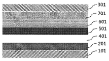
- FIG. 1 illustrates an organic solar cell according to an exemplary embodiment.
- FIG. 2 shows the observation of the color change of polyethyleneimine (PEI) and oxidized polyethyleneimine (M-PEI).
- Figure 3 is an example comparing the absorption spectrum of polyethyleneimine (PEI) and oxidized polyethyleneimine (M-PEI).
- PEI polyethyleneimine
- M-PEI oxidized polyethyleneimine
- One embodiment of the present specification is a cathode; An anode provided opposite the cathode; An organic active layer provided between the cathode and the anode; And an electron transport layer provided between the cathode and the organic active layer, wherein the electron transport layer includes an oxidized nonconjugated polymer electrolyte.
- another exemplary embodiment of the present specification is a cathode; An anode provided opposite the cathode; An organic active layer provided between the cathode and the anode; An electron transport layer provided between the cathode and the organic active layer; And a coating layer provided between the organic active layer and the electron transport layer, wherein the coating layer includes an oxidized nonconjugated polymer electrolyte.
- the organic electronic device of the present invention may be manufactured by a conventional method and material for manufacturing an organic electronic device, except that the oxidized nonconjugated polymer electrolyte is included in the electron transport layer or the coating layer.
- the organic active layer of the present invention may be a photoactive layer or a light emitting layer.
- One embodiment of the present specification is a cathode; An anode provided opposite the cathode; A photoactive layer provided between the cathode and the anode; And an electron transport layer provided between the cathode and the photoactive layer, wherein the electron transport layer comprises an oxidized nonconjugated polymer electrolyte.
- another exemplary embodiment of the present specification is a cathode; An anode provided opposite the cathode; A photoactive layer provided between the cathode and the anode; An electron transport layer provided between the cathode and the photoactive layer; And a coating layer provided between the photoactive layer and the electron transport layer, wherein the coating layer includes an oxidized nonconjugated polymer electrolyte.
- the non-conjugated polymer electrolyte means a polymer that does not include a conjugated group and includes an electrolyte group as a repeating unit, and has a charge separated from an anion and a cation in an aqueous solution. ).
- the oxidized nonconjugated polymer electrolyte is oxidized using a peroxide-based oxidant.
- the peroxide oxidant may be an organic peroxide.
- the peroxide oxidant may be hydrogen peroxide (H 2 O 2 ).
- water may remain as a reaction material after oxidation, and thus may not affect the properties of the nonconjugated polymer electrolyte.
- oxidation means that the cation is formed while the electrons in the nonconjugated polymer electrolyte are separated, and is bonded to the anion of oxygen.
- the amine group (-NR 2, R is hydrogen or a monovalent organic group) is reacted with hydrogen peroxide in non-conjugated polymer electrolyte containing a non-conjugated polymer electrolyte -N + R 2 O - to contain ionic groups in the It means modified.
- non-conjugated polymer electrolyte oxidation is -NR 2 + O - and -COOH + O -, and includes at least one of the R is hydrogen; Or a monovalent organic group.
- the oxidized nonconjugated polymer electrolyte includes at least one of hydroxylamine, nitrone, oxazirane, and N-oxide. .
- the material before oxidation of the oxidized nonconjugated polymer electrolyte includes at least one of -NR 2 and -COOH, wherein R is hydrogen; Or a monovalent organic group.
- the monovalent organic group refers to a functional group other than hydrogen, and a halogen group; Nitro group; Cyano group; Carboxyl groups; Hydroxyl group; Carbonyl group; Sulfo groups; An alkyl group; Allyl group; An alkoxy group; Cycloalkyl group; Alkenyl groups; Ester group; Ether group; Drinking time; Arylalkyl group; Aryl group; And heterocyclic groups, and the like, and may be substituted or unsubstituted with additional substituents, but are not limited thereto.
- the nonconjugated polymer electrolyte is polyethyleneimine (PEI); Polyethyleneimineethoxylate (PEIE); And polyacrylic acid (PAA) is selected from the group consisting of 1 or 2 or more.
- the weight average molecular weight of the material before oxidation of the oxidized nonconjugated polymer electrolyte is 6,000 g / mol to 1,000,000 g / mol.
- thin film formation may be easy in manufacturing an organic solar cell.
- an electron transport layer including the oxidized nonconjugated polymer electrolyte is provided in contact with a cathode.
- the oxidized nonconjugated polymer electrolyte forms a thin film of several nanometers by the dipole moment, thereby changing the work function of the cathode.
- the coating layer is provided in contact with the electron transport layer.
- the coating layer is provided in contact with the electron transport layer.
- An organic solar cell including an electron transport layer or a coating layer including an oxidized nonconjugated polymer electrolyte may be an electron donor material, which may not be applicable to a case where a nonconjugated polymer electrolyte is not conventionally oxidized. It can be used, and those skilled in the art can easily adjust the material of the organic solar cell as needed, and high efficiency of the organic solar cell can be expected.
- a non-conjugated polyelectrolyte (NPE) was used as the electron transport layer. Since the nonconjugated polymer electrolyte is a nonconductor, an ultrathin film of 1 nm to 2 nm may be formed to change the work function of the cathode without disturbing the flow of current.
- NPE non-conjugated polyelectrolyte
- the electron transport layer or coating layer including the oxidized nonconjugated polymer electrolyte has a characteristic of a dipole formed due to oxidation
- the work function of the cathode can be modified without disturbing the current flow even at an ultrathin thickness or more. It is advantageous economically and costly.
- the conductivity is increased has the advantage that the coating can be carried out in a relatively wide range.
- the ultraviolet ray in the organic solar cell is a factor that inhibits the life of the photoactive layer
- the oxidized nonconjugated polymer electrolyte according to one embodiment of the present specification absorbs ultraviolet rays, and thus has an advantageous effect on the life of the organic solar cell.
- 3 is an example comparing absorption spectra of a nonconjugated polymer electrolyte and an oxidized nonconjugated polymer electrolyte. 3, it can be seen that the oxidized nonconjugated polymer electrolyte absorbs ultraviolet rays, which is advantageous in the life of the photoactive layer.
- Figure 2 shows the observation of the color change of the non-conjugated polymer electrolyte and the oxidized non-conjugated polymer electrolyte.
- the organic electronic device includes an electron transport layer or a coating layer including an oxidized nonconjugated polymer electrolyte, so that the thickness can be adjusted as needed, thereby inducing high efficiency of the organic electronic device.
- the thickness of the electron transport layer or the coating layer including the oxidized nonconjugated polymer electrolyte is not more than an ultrathin film, but is 1 nm or more and 15 nm or less.
- the organic electronic device includes an organic material layer including an oxidized nonconjugated polymer electrolyte, and thus may be applied in various thicknesses than conventional thicknesses while maintaining efficiency.
- the organic electronic device has an inverted structure.
- the inverted structure may mean that a cathode is formed on a substrate.
- an electrode formed on a substrate may be a cathode.
- FIG. 1 illustrates an organic solar cell according to an exemplary embodiment.
- FIG. 1 includes a substrate 101, a cathode 201, an electron transport layer 401, a coating layer 501, a photoactive layer 601, a hole transport layer 701, and an anode 301.
- 1 is an exemplary structure according to an exemplary embodiment of the present specification, and may further include another organic material layer.
- the organic electronic device of the inverted structure of the present specification may mean that the anode and the cathode of the organic electronic device having the general structure are configured in the reverse direction.
- Al layer used in the organic electronic device of the general structure is very vulnerable to oxidation reaction in the air, it is difficult to ink, there is a limitation in commercializing it through the printing process.
- the reverse structure of the organic electronic device of the present specification can use Ag instead of Al, it is more stable to the oxidation reaction than the organic electronic device of the general structure, and the production of Ag ink is easy, which is advantageous for commercialization through the printing process. There is this.
- the substrate may be a glass substrate or a transparent plastic substrate having excellent transparency, surface smoothness, ease of handling, and waterproofness, but is not limited thereto, and the substrate is not limited as long as it is a substrate commonly used in organic electronic devices.
- the substrate is not limited as long as it is a substrate commonly used in organic electronic devices.
- PET polyethylene terephthalate
- PEN polyethylene naphthalate
- PP polypropylene
- PI polyimide
- TAC triacetyl cellulose
- the cathode may be a transparent conductive oxide layer or a metal electrode.
- the electrode of the present specification is a transparent conductive oxide layer
- the electrode is in addition to glass and quartz plate polyethylene terephthalate (PET), polyethylene naphthealate (PEN), polypropylene (PP), polyimide (PI), polycarbonate (PC), PS (
- a conductive material is formed on a flexible and transparent material such as polystyrene, polyoxymethylene (POM), acrylonitrile styrene (AS) resin, acrylonitrile butadiene styrene (ABS) resin, triacetyl cellulose (TAC) and polyarylate (PAR). Doped may be used.
- ITO indium tin oxide
- FTO fluorine doped tin oxide
- AZO aluminum doped zinc oxide
- IZO indium zinc oxide
- ZnO-Ga 2 O 3 ZnO-Al 2 O 3 and antimony tin oxide (ATO)
- ATO antimony tin oxide
- the anode may be a metal electrode.
- the metal electrode includes silver (Ag), aluminum (Al), platinum (Pt), tungsten (W), copper (Cu), molybdenum (Mo), gold (Au), nickel (Ni), and palladium (Pd). It may include one or two or more selected from the group consisting of. More specifically, the metal electrode may be silver (Ag).
- the electron transport layer material may be electron-extracting metal oxides, specifically, a metal complex of 8-hydroxyquinoline; Complexes including Alq 3 ; Metal complexes including Liq; LiF; Ca; Titanium oxide (TiO x ); Zinc oxide (ZnO); And cesium carbonate (Cs 2 CO 3), but it may include, but are not limited thereto.
- the cathode is a first electrode, and the anode is a second electrode.
- the anode is a first electrode
- the cathode is a second electrode
- the organic active layer includes an electron donor material and an electron acceptor material.
- the electron donor material and the electron acceptor material may mean an organic active material.
- the ratio of the electron donor material and the electron acceptor material in the organic active layer may be adjusted by those skilled in the art as needed.
- the organic active layer may be a photoactive layer.
- the photoactive layer forms an exciton in which the electron donor material pairs electrons and holes by photoexcitation, and the exciton is separated into electrons and holes at an interface of the electron donor / electron acceptor.
- the separated electrons and holes move to the electron donor material and the electron acceptor material, respectively, and they are collected at the cathode and the anode, respectively, so that they can be used as electrical energy from the outside.
- the photoactive layer may be a bulk heterojunction structure or a double layer junction structure.
- the bulk heterojunction structure may be a bulk heterojunction (BHJ) junction type
- the bilayer junction structure may be a bi-layer junction type.
- the electron donor material is at least one electron donor; Or a polymer of at least one kind of electron acceptor and at least one kind of electron donor.
- the electron donor material includes at least one kind of electron donor.
- the electron donor material also includes a polymer of at least one kind of electron acceptor and at least one kind of electron donor.
- the electron donor material is thiophene-based, fluorene-based, carbazole-based, etc. starting with MEH-PPV (poly [2-methoxy-5- (2'-ethyl-hexyloxy) -1,4-phenylene vinylene]) It can be a variety of high molecular and monomolecular materials.
- the monomolecular substance is copper (II) phthalocyanine, zinc phthalocyanine, tris [4- (5-dicynomethylidemethyl-2-thienyl) phenyl] Amine (tris [4- (5-dicyanomethylidenemethyl-2-thienyl) phenyl] amine), 2,4-bis [4- (N, N-dibenzylamino) -2,6-dihydroxyphenyl] squalane (2,4-bis [4- (N, N-dibenzylamino) -2,6-dihydroxyphenyl] squaraine), benz [b] anthracene and pentacene It may include one or more materials.
- the polymer material is poly 3-hexyl thiophene (P3HT: poly 3-hexyl thiophene), PCDTBT (poly [N-9'-heptadecanyl-2,7-carbazole-alt-5,5- (4'-) 7'-di-2-thienyl-2 ', 1', 3'-benzothiadiazole)]), PCPDTBT (poly [2,6- (4,4-bis- (2, ethylhexyl) -4H-cyclopenta [2, 1-b; 3,4-b '] dithiophene) -alt-4,7- (2,1,3-benzothiadiazole)]), PFO-DBT (poly [2,7- (9,9-dioctyl-fluorene) ) -alt-5,5- (4,7-di 2-thienyl-2,1,3-benzothiadiazole)]), PTB7 (Poly [[4,8-bis [(
- n means the repeating number of each unit.
- the electron donor material is PTB7; A polymer comprising a first unit represented by Formula 1 below and a second unit represented by Formula 2 below; Or a polymer comprising one or two or more units selected from the group consisting of units represented by formula 1-1 and units represented by formula 1-2 below.
- X1 and X2 are the same as or different from each other, and each independently CRR ', NR, O, SiRR', PR, S, GeRR ', Se or Te,
- Y1 to Y4 are the same as or different from each other, and each independently CR ′′, N, SiR ′′, P, or GeR ′′,
- X, X ', X "and X"' are the same as or different from each other, and each independently S or Se,
- A1 and A2 are the same as or different from each other, and each independently hydrogen; Or fluorine,
- L1 and L2 are the same as or different from each other, and each independently a direct bond; O; Or S,
- A3 and A4 are the same as or different from each other, and each independently hydrogen; Fluorine; Substituted or unsubstituted alkyl group; Substituted or unsubstituted aryl group; Or a substituted or unsubstituted heterocyclic group,
- At least one of L1 and L2 is O or S,
- R, R ', R "and R1 to R8 are the same as or different from each other, and each independently hydrogen; deuterium; halogen; hydroxy group; substituted or unsubstituted alkyl group; substituted or unsubstituted alkoxy group; substituted or unsubstituted An aryl group or a substituted or unsubstituted heterocyclic group,
- a1 to a4 are each an integer of 0 or 1
- x is the mole fraction, where 0 ⁇ x ⁇ 1,
- y is the mole fraction, where 0 ⁇ y ⁇ 1,
- p is the mole fraction, where 0 ⁇ p ⁇ 1,
- q is the mole fraction, where 0 ⁇ q ⁇ 1,
- z and r are each an integer from 1 to 10,000,
- R11 to R19 are the same as or different from each other, and each independently hydrogen; Substituted or unsubstituted alkyl group; Or a substituted or unsubstituted alkoxy group.
- R11 is a substituted or unsubstituted alkoxy group.
- R11 is a substituted or unsubstituted octoxy group.
- R11 is an octoxy group.
- R12 is a substituted or unsubstituted alkoxy group.
- R12 is a substituted or unsubstituted octoxy group.
- R12 is an octoxy group.
- R13 is a substituted or unsubstituted alkyl group.
- R13 is a substituted or unsubstituted dodecanyl group.
- R13 is a dodecanyl group.
- R14 is a substituted or unsubstituted alkyl group.
- R14 is a linear or branched alkyl group.
- R14 is a substituted or unsubstituted 2-ethylhexyl group.
- R14 is a 2-ethylhexyl group.
- R15 is a substituted or unsubstituted alkyl group.
- R15 is a linear or branched alkyl group.
- R15 is a substituted or unsubstituted 2-ethylhexyl group.
- R15 is a 2-ethylhexyl group.
- R16 is a substituted or unsubstituted alkyl group.
- R16 is a substituted or unsubstituted dodecanyl group.
- R16 is a dodecanyl group.
- R17 is hydrogen
- R18 is hydrogen
- R19 is a substituted or unsubstituted alkyl group.
- R19 is a substituted or unsubstituted dodecanyl group.
- R19 is a dodecanyl group.
- the unit represented by Chemical Formula 1-1 is represented by the following Chemical Formula 1-11.
- the unit represented by Chemical Formula 1-2 is represented by the following Chemical Formula 1-22.
- the end group of the polymer is a substituted or unsubstituted heterocyclic group or a substituted or unsubstituted aryl group.
- the end group of the polymer is 4- (trifluoromethyl) phenyl group (4- (trifluoromethyl) phenyl).
- X1 is S.
- Y1 is N.
- Y2 is N.
- the a1 is 1.
- the a2 is 1.
- R2 is hydrogen
- R3 is hydrogen
- the first unit represented by Formula 1; And a polymer comprising a second unit represented by the formula (2) is represented by the formula (3).
- A3 and A4 are the same as or different from each other, and are each independently a substituted or unsubstituted alkyl group.
- A3 and A4 are the same as or different from each other, and are each independently a substituted or unsubstituted alkyl group having 1 to 30 carbon atoms.
- A3 and A4 are substituted or unsubstituted dodecyl groups.
- A3 is a dodecyl group.
- A4 is a dodecyl group.
- R1 and R4 are the same as or different from each other, and are each independently a substituted or unsubstituted alkyl group.
- R1 and R4 are the same as or different from each other, and are each independently a substituted or unsubstituted alkyl group having 1 to 30 carbon atoms.
- R1 and R4 are the same as or different from each other, and each independently a substituted or unsubstituted linear or branched alkyl group having 1 to 30 carbon atoms.
- R1 and R4 are the same as or different from each other, and are each independently a substituted or unsubstituted 2-ethylhexyl group.
- R1 and R4 are the same as or different from each other, and are each independently a substituted or unsubstituted 2-octyldecyl group.
- R1 is a 2-ethylhexyl group.
- R4 is a 2-ethylhexyl group.
- R1 is a 2-ethyloctyl group.
- R4 is a 2-ethyloctyl group.
- R1 is a 2-ethyldecyl group.
- R4 is a 2-ethyldecyl group.
- R1 is a 2-ethyldodecyl group.
- R4 is a 2-ethyldodecyl group.
- R1 is a 2-butyloctyl group.
- R4 is a 2-butyloctyl group.
- R1 is a 2-octyldecyl group.
- R4 is a 2-octyldecyl group.
- the end group of the polymer is a substituted or unsubstituted heterocyclic group or a substituted or unsubstituted aryl group.
- the polymer includes a unit represented by the following formula (4).
- n is a repetition number of units and is an integer of 1 to 10,000.
- l is 0.5.
- m is 0.5.
- the electron acceptor material may be a fullerene derivative or a nonfullerene derivative.
- the fullerene derivative is a fullerene derivative of C60 to C90.
- the fullerene derivative may be a C60 fullerene derivative or a C70 fullerene derivative.
- the fullerene derivative may be unsubstituted or substituted with additional substituents.
- the fullerene derivative has an ability to separate electron-hole pairs (exciton, electron-hole pair) and charge mobility compared to the non-fullerene derivative, which is advantageous for efficiency characteristics.
- the organic electronic device is one or more organic material layer selected from the group consisting of a hole injection layer, a hole transport layer, a hole blocking layer, a charge generating layer, an electron blocking layer, an electron injection layer and an electron transport layer. It includes more.
- the hole transport layer and / or the electron transport layer material serves to efficiently transfer electrons and holes separated from the organic active layer to the electrode, and the material is not particularly limited.
- the hole transport layer material is PEDOT: PSS (Poly (3,4-ethylenedioxythiophene) doped with poly (styrenesulfonate)), molybdenum oxide (MoO x ); Vanadium oxide (V 2 O 5); Nickel oxide (NiO); Tungsten oxide (WO x ), and the like, but is not limited thereto.
- PSS Poly (3,4-ethylenedioxythiophene) doped with poly (styrenesulfonate)
- MoO x molybdenum oxide
- V 2 O 5 Vanadium oxide
- NiO Nickel oxide
- WO x Tungsten oxide
- One embodiment of the present specification comprises the steps of preparing a substrate; Forming a cathode on the substrate; Forming an electron transport layer on the cathode; Forming an organic active layer on the electron transport layer; And forming an anode on the organic active layer, wherein the electron transport layer comprises an oxidized nonconjugated polymer electrolyte.
- One embodiment of the present specification comprises the steps of preparing a substrate; Forming a cathode on the substrate; Forming an electron transport layer on the cathode; Forming a coating layer on the electron transport layer; Forming an organic active layer on the coating layer; And forming an anode on the organic active layer, wherein the coating layer comprises an oxidized nonconjugated polymer electrolyte.
- the substrate, the cathode, the electron transport layer, the oxidized nonconjugated polymer electrolyte, the organic active layer, and the anode are the same as described above.
- the forming of the electron transport layer or the coating layer including the oxidized nonconjugated polymer electrolyte comprises oxidizing the nonconjugated polymer electrolyte with a peroxide oxidant; And forming an organic layer including the oxidized nonconjugated polymer electrolyte.
- the step of forming an electron transport layer or a coating layer comprising the oxidized nonconjugated polymer electrolyte comprises oxidizing the nonconjugated polymer electrolyte with hydrogen peroxide; And forming an organic layer including the oxidized nonconjugated polymer electrolyte.
- one or more organic material layers selected from the group consisting of a hole injection layer, a hole transport layer, a hole blocking layer, a charge generating layer, an electron blocking layer, an electron injection layer and an electron transport layer between each step. It may further comprise the step of laminating.
- An organic electronic device may use a known method except that it includes an electron transport layer or a coating layer including an oxidized nonconjugated polymer electrolyte.
- the forming of the anode and / or the cathode may be performed by sequentially cleaning the patterned ITO substrate with a detergent, acetone, and isopropanol (IPA), and then heating the plate at 100 ° C. to 250 ° C. in order to remove moisture. 1 minute to 30 minutes, specifically, dried at 250 °C for 10 minutes, when the substrate is thoroughly cleaned, the surface of the substrate can be modified to hydrophilic.
- Pretreatment techniques for this purpose include a) surface oxidation using parallel planar discharge, b) oxidation of the surface through ozone generated using UV ultraviolet light in a vacuum state, and c) oxygen radicals generated by plasma. The oxidation method etc. can be used.
- the bonding surface potential can be maintained at a level suitable for the surface potential of the hole injection layer, the formation of the polymer thin film on the ITO substrate can be facilitated, and the quality of the thin film can be improved.
- One of the above methods is selected according to the state of the substrate, and any method may be used to prevent oxygen escape from the surface of the substrate and to minimize the residual of moisture and organic matters in order to expect a substantial effect of pretreatment.
- a method of oxidizing the surface through ozone generated by using UV was used, and after the ultrasonic cleaning, the patterned ITO substrate was baked on a hot plate and dried well. It is then put into a chamber and a UV lamp is activated to clean the ITO substrate patterned by ozone generated by oxygen gas reacting with UV light.
- the surface modification method of the patterned ITO substrate in this invention does not need to specifically limit, Any method may be used as long as it is a method of oxidizing a substrate.
- the electron transport layer of the present specification is formed by being applied to one side of the cathode or coated in the form of a film using sputtering, E-Beam, thermal deposition, spin coating, screen printing, inkjet printing, doctor blade, slot-die or gravure printing method Can be.
- the photoactive layer in the present specification may be formed into a thickness in the range of 50nm to 280nm by a method such as spin coating after dissolving the above-described photoactive materials in an organic solvent.
- the photoactive layer may apply a method such as dip coating, screen printing, spray coating, doctor blade or brush painting.
- ITO was formed as a first electrode on the substrate, and the electron transport layer was formed by spin-coating ZnO on the ITO.
- the hole transport layer was formed by the method of depositing the MoO 3 (8nm to 20nm) on the photoactive layer, and finally forming a second electrode on the method of depositing the Ag (100nm to 200nm) on the hole transport layer.
- An organic solar cell was manufactured in the same manner as in Example 1, except that PC 61 BM and a copolymer represented by the following formula were used to form the photoactive layer in Example 1.
- An organic solar cell was manufactured in the same manner as in Example 1, except that PC 71 BM and PTB7 (purchased from 1-material) were used to form the photoactive layer in Example 1.
- An organic solar cell was manufactured in the same manner as in Example 1, except that the ZnO layer was not formed on ITO in Example 1.
- An organic solar cell was manufactured in the same manner as in Example 2, except that the ZnO layer was not formed on ITO in Example 2.
- ITO was formed as a first electrode on the substrate, and an electron transport layer was formed by spin-coating a material obtained by oxidizing polyethyleneimine (PEI) with hydrogen peroxide on the ITO.
- PEI polyethyleneimine
- the hole transport layer was formed by depositing MoO 3 (8 nm to 20 nm) on the photoactive layer, and finally, a second electrode was formed by depositing Ag (100 nm to 200 nm) on the hole transport layer.
- Example 6 PC 61 BM and when to form the optically active layer was prepared in the and the organic solar cell in the same manner as in Example 6 except for using a copolymer represented by the following formula.
- An organic solar cell was manufactured in the same manner as in Example 1, except that the nonconjugated polymer electrolyte layer was not formed in Example 1.
- An organic solar cell was manufactured in the same manner as in Example 1, except that polyethyleneimine (PEI) was used instead of the oxidized polyethyleneimine in Example 1.
- PEI polyethyleneimine
- Example 2 an organic solar cell was manufactured in the same manner as in Example 2, except that a separate oxidized nonconjugated polymer electrolyte layer was not formed on ZnO.
- Example 3 an organic solar cell was manufactured in the same manner as in Example 3, except that a separate nonconjugated polymer electrolyte layer was not formed on ZnO.
- Example 3 an organic solar cell was manufactured in the same manner as in Example 3, except that an electron transport layer was not formed of ZnO on ITO.
- An organic solar cell was manufactured in the same manner as in Example 6, except that polyethyleneimine (PEI) was used instead of the oxidized polyethyleneimine in Example 6.
- PEI polyethyleneimine
- An organic solar cell was manufactured in the same manner as in Example 7, except that polyethyleneimine (PEI) was used instead of the oxidized polyethyleneimine in Example 7.
- PEI polyethyleneimine
- An organic solar cell was manufactured in the same manner as in Example 5, except that polyethyleneimine (PEI) was used instead of the oxidized polyethyleneimine in Example 5.
- PEI polyethyleneimine
- Example 1 0.759 16.441 0.691 8.62 8.59 0.758 16.184 0.699 8.57 0.758 16.098 0.702 8.57
- Example 2 0.949 13.100 0.638 7.93 8.14 0.941 13.373 0.649 8.17 0.945 13.321 0.660 8.31
- Example 3 0.685 16.322 0.654 7.32 7.32 0.684 16.335 0.656 7.33 0.688 16.156 0.658 7.32
- Example 5 0.943 13.222 0.633 7.90 7.88 0.943 13.313 0.620 7.78 0.938 13.333 0.636 7.95
- Example 6 0.650 8.795 0.728 4.16 4.13 0.645 8.808 0.722 4.10
- Example 7 0.867 13.330 0.651 7.53 7.50 0.863 13.204 0.655 7.
- V oc denotes an open voltage
- J sc denotes a short circuit current
- FF denotes a fill factor
- ⁇ denotes a power conversion efficiency (PCE).
- the open-circuit and short-circuit currents are the X- and Y-axis intercepts in the four quadrants of the voltage-current density curve, respectively. The higher these two values, the higher the efficiency of the solar cell.
- the fill factor is the area of the rectangle drawn inside the curve divided by the product of the short circuit current and the open voltage. By dividing these three values by the intensity of the emitted light, the energy conversion efficiency can be obtained, and higher values are preferable.
- Example 1 when comparing only the case of the formation of the nonconjugated polymer electrolyte layer oxidized under the same conditions, Example 1 compared to Comparative Example 1, Example 2 compared to Comparative Example 3, compared to Comparative Example 4 It can be seen that Example 3 exhibits excellent efficiency.
- Example 1 compared to Comparative Example 2
- Example 6 compared to Comparative Example 6
- Example 7 compared to Comparative Example 7, and Comparative Example 8
- Example 5 showed more excellent efficiency.
Landscapes
- Chemical & Material Sciences (AREA)
- Health & Medical Sciences (AREA)
- Chemical Kinetics & Catalysis (AREA)
- Medicinal Chemistry (AREA)
- Polymers & Plastics (AREA)
- Organic Chemistry (AREA)
- Physics & Mathematics (AREA)
- Electromagnetism (AREA)
- Engineering & Computer Science (AREA)
- Materials Engineering (AREA)
- Nanotechnology (AREA)
- Photovoltaic Devices (AREA)
- Electroluminescent Light Sources (AREA)
Abstract
La présente invention concerne un élément électronique organique et un procédé de fabrication de celui-ci, l'élément électronique organique comprenant : une cathode ; une anode disposée de manière à faire face à la cathode ; une couche active organique disposée entre la cathode et l'anode ; et une couche de transport d'électrons disposée entre la cathode et la couche active organique, la couche de transport d'électrons contenant un électrolyte polymère non conjugué oxydé.
Priority Applications (3)
| Application Number | Priority Date | Filing Date | Title |
|---|---|---|---|
| EP17806877.1A EP3451399B1 (fr) | 2016-06-03 | 2017-03-29 | Élément électronique organique et procédé de fabrication de celui-ci |
| CN201780033451.7A CN109196677B (zh) | 2016-06-03 | 2017-03-29 | 有机电子元件及用于制造其的方法 |
| US16/304,004 US10662313B2 (en) | 2016-06-03 | 2017-03-29 | Organic electronic element and method for manufacturing same |
Applications Claiming Priority (2)
| Application Number | Priority Date | Filing Date | Title |
|---|---|---|---|
| KR20160069834 | 2016-06-03 | ||
| KR10-2016-0069834 | 2016-06-03 |
Publications (1)
| Publication Number | Publication Date |
|---|---|
| WO2017209384A1 true WO2017209384A1 (fr) | 2017-12-07 |
Family
ID=60478839
Family Applications (1)
| Application Number | Title | Priority Date | Filing Date |
|---|---|---|---|
| PCT/KR2017/003410 Ceased WO2017209384A1 (fr) | 2016-06-03 | 2017-03-29 | Élément électronique organique et procédé de fabrication de celui-ci |
Country Status (5)
| Country | Link |
|---|---|
| US (1) | US10662313B2 (fr) |
| EP (1) | EP3451399B1 (fr) |
| KR (1) | KR101966853B1 (fr) |
| CN (1) | CN109196677B (fr) |
| WO (1) | WO2017209384A1 (fr) |
Cited By (1)
| Publication number | Priority date | Publication date | Assignee | Title |
|---|---|---|---|---|
| EP3953967A1 (fr) | 2019-04-10 | 2022-02-16 | 10644137 Canada Inc. | Appareil à énergie hybride, système et procédé associé |
Families Citing this family (8)
| Publication number | Priority date | Publication date | Assignee | Title |
|---|---|---|---|---|
| KR102134507B1 (ko) | 2017-03-21 | 2020-07-16 | 주식회사 엘지화학 | 화합물 및 이를 포함하는 유기 태양 전지 |
| WO2019013486A1 (fr) | 2017-07-10 | 2019-01-17 | 주식회사 엘지화학 | Dispositif électrochrome comprenant un composé électrochrome et son procédé de fabrication |
| KR102120532B1 (ko) | 2017-09-18 | 2020-06-16 | 주식회사 엘지화학 | 유기트랜지스터 |
| KR102250385B1 (ko) * | 2017-10-18 | 2021-05-11 | 주식회사 엘지화학 | 유기 광 다이오드 및 이를 포함하는 유기 이미지 센서 |
| KR102116655B1 (ko) | 2018-12-03 | 2020-06-01 | 연세대학교 산학협력단 | 산화물 반도체 박막 트랜지스터 |
| JP7293026B2 (ja) * | 2019-07-30 | 2023-06-19 | 住友化学株式会社 | π共役系ポリマーの製造方法 |
| CN110459681A (zh) * | 2019-07-31 | 2019-11-15 | 青岛大学 | 基于聚乙烯亚胺修饰的氧化锌电子传输层构建柔性结构的聚合物太阳能电池及其制备方法 |
| KR102227722B1 (ko) * | 2019-11-22 | 2021-03-16 | 한국재료연구원 | 광전소자용 전자 수송 재료 및 이를 포함하는 광전소자 |
Citations (7)
| Publication number | Priority date | Publication date | Assignee | Title |
|---|---|---|---|---|
| KR20040017761A (ko) * | 2002-08-23 | 2004-02-27 | 삼성전자주식회사 | 유기 스트리핑 조성물 및 이를 사용한 산화물 식각 방법 |
| KR20130133571A (ko) * | 2012-05-29 | 2013-12-09 | 광주과학기술원 | 아민기를 갖는 비공액 고분자를 포함하는 유기전자소자용 기능층 및 이를 포함하는 유기전자소자 |
| KR20140101041A (ko) * | 2013-02-07 | 2014-08-19 | 광주과학기술원 | 고분자 태양전지 및 이의 제조방법 |
| KR20140143044A (ko) | 2013-06-05 | 2014-12-15 | 삼성테크윈 주식회사 | 압축기 케이싱, 이의 제조 방법 및 이를 구비하는 원심 압축기 |
| KR20150020471A (ko) | 2013-08-16 | 2015-02-26 | 현대중공업 주식회사 | 선박 건조 방법 |
| KR20150125618A (ko) * | 2014-04-30 | 2015-11-09 | 주식회사 엘지화학 | 태양 전지 및 이의 제조 방법 |
| KR20160067340A (ko) * | 2014-12-04 | 2016-06-14 | 주식회사 엘지화학 | 유기 태양 전지 및 이의 제조방법 |
Family Cites Families (16)
| Publication number | Priority date | Publication date | Assignee | Title |
|---|---|---|---|---|
| US5331183A (en) | 1992-08-17 | 1994-07-19 | The Regents Of The University Of California | Conjugated polymer - acceptor heterojunctions; diodes, photodiodes, and photovoltaic cells |
| KR101571116B1 (ko) | 2008-11-13 | 2015-11-24 | 삼성전자주식회사 | 유기 물질, 상기 유기 물질을 포함한 필름, 상기 필름을 구비한 전기 소자 |
| KR101121165B1 (ko) | 2010-05-26 | 2012-03-20 | 광주과학기술원 | P?도핑된 공액 고분자 전해질 및 이를 이용한 유기전자소자 |
| EP2710611B1 (fr) * | 2011-05-16 | 2019-03-20 | Georgia Tech Research Corporation | Procédés de fabrication d'électrodes à faible travail d'extraction et électrode à faible travail d'extraction |
| US10347867B2 (en) * | 2012-09-24 | 2019-07-09 | The Texas A&M University System | Multilayer barrier film |
| KR20140122655A (ko) * | 2013-04-10 | 2014-10-20 | 포항공과대학교 산학협력단 | 역구조 유기 발광 다이오드 및 이의 제조방법 |
| KR20160085309A (ko) * | 2013-11-12 | 2016-07-15 | 피피지 인더스트리즈 오하이오 인코포레이티드 | 광기전 시스템 및 광기전 시스템을 제조하기 위한 분무 코팅 방법 |
| KR101587895B1 (ko) | 2013-12-24 | 2016-01-22 | 광주과학기술원 | 역구조 유기 전자소자 및 그의 제조방법 |
| CN103811663A (zh) * | 2014-02-27 | 2014-05-21 | 西南大学 | 一种免退火的有机太阳能电池及其制备方法 |
| KR20150121407A (ko) | 2014-04-21 | 2015-10-29 | 주식회사 엘지화학 | 텐덤형 유기태양전지 및 이의 제조방법 |
| KR101684636B1 (ko) | 2014-08-07 | 2016-12-08 | 광주과학기술원 | P-도핑된 공액 고분자 전해질 및 이를 이용한 유기전자소자 |
| CN104393175A (zh) * | 2014-10-16 | 2015-03-04 | 南昌大学 | 一种有机太阳能电池及制备方法 |
| CN104538554B (zh) * | 2015-01-13 | 2017-01-25 | 北京科技大学 | 具有双组分混合电子传输/空穴阻挡层有机发光二极管 |
| WO2016120721A1 (fr) | 2015-01-27 | 2016-08-04 | King Abdullah University Of Science And Technology | Dispositifs optoélectroniques, procédés de préparation à basse température, et couches de transport d'électrons améliorées |
| CN105047821B (zh) * | 2015-06-02 | 2017-07-11 | 吉林大学 | 基于活性层与传输层修饰的反型聚合物太阳能电池及制备方法 |
| CN105355791A (zh) * | 2015-11-01 | 2016-02-24 | 华南理工大学 | 一种水/醇溶型非共轭聚合物界面材料及其有机太阳电池器件与制备方法 |
-
2017
- 2017-03-29 CN CN201780033451.7A patent/CN109196677B/zh active Active
- 2017-03-29 EP EP17806877.1A patent/EP3451399B1/fr active Active
- 2017-03-29 WO PCT/KR2017/003410 patent/WO2017209384A1/fr not_active Ceased
- 2017-03-29 US US16/304,004 patent/US10662313B2/en active Active
- 2017-03-29 KR KR1020170040031A patent/KR101966853B1/ko active Active
Patent Citations (7)
| Publication number | Priority date | Publication date | Assignee | Title |
|---|---|---|---|---|
| KR20040017761A (ko) * | 2002-08-23 | 2004-02-27 | 삼성전자주식회사 | 유기 스트리핑 조성물 및 이를 사용한 산화물 식각 방법 |
| KR20130133571A (ko) * | 2012-05-29 | 2013-12-09 | 광주과학기술원 | 아민기를 갖는 비공액 고분자를 포함하는 유기전자소자용 기능층 및 이를 포함하는 유기전자소자 |
| KR20140101041A (ko) * | 2013-02-07 | 2014-08-19 | 광주과학기술원 | 고분자 태양전지 및 이의 제조방법 |
| KR20140143044A (ko) | 2013-06-05 | 2014-12-15 | 삼성테크윈 주식회사 | 압축기 케이싱, 이의 제조 방법 및 이를 구비하는 원심 압축기 |
| KR20150020471A (ko) | 2013-08-16 | 2015-02-26 | 현대중공업 주식회사 | 선박 건조 방법 |
| KR20150125618A (ko) * | 2014-04-30 | 2015-11-09 | 주식회사 엘지화학 | 태양 전지 및 이의 제조 방법 |
| KR20160067340A (ko) * | 2014-12-04 | 2016-06-14 | 주식회사 엘지화학 | 유기 태양 전지 및 이의 제조방법 |
Non-Patent Citations (2)
| Title |
|---|
| GU, XUEHUI ET AL.: "Influences of Surface Capping with Electrostatically Self-assembled PEI on the Photoresponse of Ti02 Thin Film", CHEMICAL COMMUNICATIONS, 28 May 2013 (2013-05-28), XP055556047 * |
| See also references of EP3451399A4 |
Cited By (4)
| Publication number | Priority date | Publication date | Assignee | Title |
|---|---|---|---|---|
| EP3953967A1 (fr) | 2019-04-10 | 2022-02-16 | 10644137 Canada Inc. | Appareil à énergie hybride, système et procédé associé |
| CN114080678A (zh) * | 2019-04-10 | 2022-02-22 | 10644137 加拿大公司 | 混合能源装置、系统及其方法 |
| EP3953967A4 (fr) * | 2019-04-10 | 2023-01-11 | 10644137 Canada Inc. | Appareil à énergie hybride, système et procédé associé |
| CN114080678B (zh) * | 2019-04-10 | 2025-12-09 | 10644137加拿大公司 | 混合能源装置、系统及其方法 |
Also Published As
| Publication number | Publication date |
|---|---|
| KR101966853B1 (ko) | 2019-04-08 |
| EP3451399B1 (fr) | 2020-04-29 |
| CN109196677A (zh) | 2019-01-11 |
| KR20170137612A (ko) | 2017-12-13 |
| EP3451399A1 (fr) | 2019-03-06 |
| US10662313B2 (en) | 2020-05-26 |
| EP3451399A4 (fr) | 2019-05-15 |
| CN109196677B (zh) | 2022-04-15 |
| US20190203016A1 (en) | 2019-07-04 |
Similar Documents
| Publication | Publication Date | Title |
|---|---|---|
| WO2018021794A1 (fr) | Procédé de préparation d'un film de composé de pérovskite hautement efficace et cellule solaire le comprenant | |
| WO2014109604A1 (fr) | Cellule solaire hybride organique-inorganique durable et haute performance | |
| WO2014200309A1 (fr) | Cellule photovoltaïque organique et son procédé de fabrication | |
| WO2014109610A1 (fr) | Procédé de fabrication d'une cellule solaire hybride organique-inorganique à haut rendement | |
| WO2015167285A1 (fr) | Cellule solaire et son procédé de fabrication | |
| WO2016099218A2 (fr) | Polymère et cellule solaire organique comprenant ce polymère | |
| WO2018216880A1 (fr) | Composé hétérocyclique et dispositif électronique organique le comprenant | |
| US10662313B2 (en) | Organic electronic element and method for manufacturing same | |
| WO2015167284A1 (fr) | Cellule solaire organique et procédé de fabrication associé | |
| WO2015163614A1 (fr) | Composé hétérocyclique et cellule solaire organique le comprenant | |
| WO2021107674A1 (fr) | Nouveau composé et dispositif électronique organique l'utilisant | |
| WO2014119962A1 (fr) | Nouveau matériau polymère destiné à une cellule solaire à couche mince organique hautement efficace et cellule solaire à film mince organique l'utilisant | |
| WO2014133373A1 (fr) | Elément électronique employant une électrode hybride ayant une fonction de travail et une conductivité élevées | |
| WO2015167225A1 (fr) | Cellule solaire organique et son procédé de fabrication | |
| WO2016171465A2 (fr) | Composé hétérocyclique et cellule solaire organique le comprenant | |
| WO2014051397A1 (fr) | Couche optiquement active, cellule solaire organique comportant une couche optiquement active et procédé de fabrication de celles-ci | |
| WO2021118238A1 (fr) | Nouveau polymère et dispositif électronique organique l'utilisant | |
| WO2021025519A1 (fr) | Élément photoélectrique pérovskite et son procédé de fabrication | |
| WO2015016626A1 (fr) | Copolymère et cellule solaire organique comprenant ledit copolymère | |
| WO2022035239A1 (fr) | Procédé de préparation d'un dispositif optoélectronique à base de pérovskite et dispositif optoélectronique à base de pérovskite préparé par ledit procédé | |
| WO2019221386A1 (fr) | Composé hétérocyclique et dispositif électronique organique le comprenant | |
| WO2015190762A2 (fr) | Dérivé à cycles fusionnés et cellule solaire organique le comprenant | |
| WO2015163658A1 (fr) | Cellule solaire organique empilée | |
| WO2018080050A1 (fr) | Cellule solaire en pérovskite et de grande surface | |
| WO2014182139A1 (fr) | Couche photo-active, cellule solaire organique la comprenant, et procédé de fabrication associé |
Legal Events
| Date | Code | Title | Description |
|---|---|---|---|
| NENP | Non-entry into the national phase |
Ref country code: DE |
|
| 121 | Ep: the epo has been informed by wipo that ep was designated in this application |
Ref document number: 17806877 Country of ref document: EP Kind code of ref document: A1 |
|
| ENP | Entry into the national phase |
Ref document number: 2017806877 Country of ref document: EP Effective date: 20181129 |