WO2017221815A1 - アクティブマトリクス基板、光シャッタ基板、表示装置、アクティブマトリクス基板の製造方法 - Google Patents
アクティブマトリクス基板、光シャッタ基板、表示装置、アクティブマトリクス基板の製造方法 Download PDFInfo
- Publication number
- WO2017221815A1 WO2017221815A1 PCT/JP2017/022245 JP2017022245W WO2017221815A1 WO 2017221815 A1 WO2017221815 A1 WO 2017221815A1 JP 2017022245 W JP2017022245 W JP 2017022245W WO 2017221815 A1 WO2017221815 A1 WO 2017221815A1
- Authority
- WO
- WIPO (PCT)
- Prior art keywords
- film
- active matrix
- metal film
- oxide semiconductor
- matrix substrate
- Prior art date
- Legal status (The legal status is an assumption and is not a legal conclusion. Google has not performed a legal analysis and makes no representation as to the accuracy of the status listed.)
- Ceased
Links
Images






Classifications
-
- G—PHYSICS
- G02—OPTICS
- G02B—OPTICAL ELEMENTS, SYSTEMS OR APPARATUS
- G02B26/00—Optical devices or arrangements for the control of light using movable or deformable optical elements
- G02B26/02—Optical devices or arrangements for the control of light using movable or deformable optical elements for controlling the intensity of light
-
- G—PHYSICS
- G02—OPTICS
- G02F—OPTICAL DEVICES OR ARRANGEMENTS FOR THE CONTROL OF LIGHT BY MODIFICATION OF THE OPTICAL PROPERTIES OF THE MEDIA OF THE ELEMENTS INVOLVED THEREIN; NON-LINEAR OPTICS; FREQUENCY-CHANGING OF LIGHT; OPTICAL LOGIC ELEMENTS; OPTICAL ANALOGUE/DIGITAL CONVERTERS
- G02F1/00—Devices or arrangements for the control of the intensity, colour, phase, polarisation or direction of light arriving from an independent light source, e.g. switching, gating or modulating; Non-linear optics
- G02F1/01—Devices or arrangements for the control of the intensity, colour, phase, polarisation or direction of light arriving from an independent light source, e.g. switching, gating or modulating; Non-linear optics for the control of the intensity, phase, polarisation or colour
- G02F1/13—Devices or arrangements for the control of the intensity, colour, phase, polarisation or direction of light arriving from an independent light source, e.g. switching, gating or modulating; Non-linear optics for the control of the intensity, phase, polarisation or colour based on liquid crystals, e.g. single liquid crystal display cells
- G02F1/133—Constructional arrangements; Operation of liquid crystal cells; Circuit arrangements
- G02F1/136—Liquid crystal cells structurally associated with a semi-conducting layer or substrate, e.g. cells forming part of an integrated circuit
- G02F1/1362—Active matrix addressed cells
- G02F1/136227—Through-hole connection of the pixel electrode to the active element through an insulation layer
-
- G—PHYSICS
- G02—OPTICS
- G02F—OPTICAL DEVICES OR ARRANGEMENTS FOR THE CONTROL OF LIGHT BY MODIFICATION OF THE OPTICAL PROPERTIES OF THE MEDIA OF THE ELEMENTS INVOLVED THEREIN; NON-LINEAR OPTICS; FREQUENCY-CHANGING OF LIGHT; OPTICAL LOGIC ELEMENTS; OPTICAL ANALOGUE/DIGITAL CONVERTERS
- G02F1/00—Devices or arrangements for the control of the intensity, colour, phase, polarisation or direction of light arriving from an independent light source, e.g. switching, gating or modulating; Non-linear optics
- G02F1/01—Devices or arrangements for the control of the intensity, colour, phase, polarisation or direction of light arriving from an independent light source, e.g. switching, gating or modulating; Non-linear optics for the control of the intensity, phase, polarisation or colour
- G02F1/13—Devices or arrangements for the control of the intensity, colour, phase, polarisation or direction of light arriving from an independent light source, e.g. switching, gating or modulating; Non-linear optics for the control of the intensity, phase, polarisation or colour based on liquid crystals, e.g. single liquid crystal display cells
- G02F1/133—Constructional arrangements; Operation of liquid crystal cells; Circuit arrangements
- G02F1/136—Liquid crystal cells structurally associated with a semi-conducting layer or substrate, e.g. cells forming part of an integrated circuit
- G02F1/1362—Active matrix addressed cells
- G02F1/1368—Active matrix addressed cells in which the switching element is a three-electrode device
-
- G—PHYSICS
- G09—EDUCATION; CRYPTOGRAPHY; DISPLAY; ADVERTISING; SEALS
- G09F—DISPLAYING; ADVERTISING; SIGNS; LABELS OR NAME-PLATES; SEALS
- G09F9/00—Indicating arrangements for variable information in which the information is built-up on a support by selection or combination of individual elements
-
- G—PHYSICS
- G09—EDUCATION; CRYPTOGRAPHY; DISPLAY; ADVERTISING; SEALS
- G09F—DISPLAYING; ADVERTISING; SIGNS; LABELS OR NAME-PLATES; SEALS
- G09F9/00—Indicating arrangements for variable information in which the information is built-up on a support by selection or combination of individual elements
- G09F9/30—Indicating arrangements for variable information in which the information is built-up on a support by selection or combination of individual elements in which the desired character or characters are formed by combining individual elements
-
- G—PHYSICS
- G09—EDUCATION; CRYPTOGRAPHY; DISPLAY; ADVERTISING; SEALS
- G09F—DISPLAYING; ADVERTISING; SIGNS; LABELS OR NAME-PLATES; SEALS
- G09F9/00—Indicating arrangements for variable information in which the information is built-up on a support by selection or combination of individual elements
- G09F9/30—Indicating arrangements for variable information in which the information is built-up on a support by selection or combination of individual elements in which the desired character or characters are formed by combining individual elements
- G09F9/37—Indicating arrangements for variable information in which the information is built-up on a support by selection or combination of individual elements in which the desired character or characters are formed by combining individual elements being movable elements
-
- H—ELECTRICITY
- H10—SEMICONDUCTOR DEVICES; ELECTRIC SOLID-STATE DEVICES NOT OTHERWISE PROVIDED FOR
- H10D—INORGANIC ELECTRIC SEMICONDUCTOR DEVICES
- H10D64/00—Electrodes of devices having potential barriers
- H10D64/01—Manufacture or treatment
- H10D64/011—Manufacture or treatment of electrodes ohmically coupled to a semiconductor
-
- H—ELECTRICITY
- H10—SEMICONDUCTOR DEVICES; ELECTRIC SOLID-STATE DEVICES NOT OTHERWISE PROVIDED FOR
- H10D—INORGANIC ELECTRIC SEMICONDUCTOR DEVICES
- H10D64/00—Electrodes of devices having potential barriers
- H10D64/20—Electrodes characterised by their shapes, relative sizes or dispositions
- H10D64/27—Electrodes not carrying the current to be rectified, amplified, oscillated or switched, e.g. gates
-
- H—ELECTRICITY
- H10—SEMICONDUCTOR DEVICES; ELECTRIC SOLID-STATE DEVICES NOT OTHERWISE PROVIDED FOR
- H10D—INORGANIC ELECTRIC SEMICONDUCTOR DEVICES
- H10D64/00—Electrodes of devices having potential barriers
- H10D64/60—Electrodes characterised by their materials
- H10D64/66—Electrodes having a conductor capacitively coupled to a semiconductor by an insulator, e.g. MIS electrodes
-
- H—ELECTRICITY
- H10—SEMICONDUCTOR DEVICES; ELECTRIC SOLID-STATE DEVICES NOT OTHERWISE PROVIDED FOR
- H10D—INORGANIC ELECTRIC SEMICONDUCTOR DEVICES
- H10D86/00—Integrated devices formed in or on insulating or conducting substrates, e.g. formed in silicon-on-insulator [SOI] substrates or on stainless steel or glass substrates
- H10D86/40—Integrated devices formed in or on insulating or conducting substrates, e.g. formed in silicon-on-insulator [SOI] substrates or on stainless steel or glass substrates characterised by multiple TFTs
- H10D86/421—Integrated devices formed in or on insulating or conducting substrates, e.g. formed in silicon-on-insulator [SOI] substrates or on stainless steel or glass substrates characterised by multiple TFTs having a particular composition, shape or crystalline structure of the active layer
- H10D86/423—Integrated devices formed in or on insulating or conducting substrates, e.g. formed in silicon-on-insulator [SOI] substrates or on stainless steel or glass substrates characterised by multiple TFTs having a particular composition, shape or crystalline structure of the active layer comprising semiconductor materials not belonging to the Group IV, e.g. InGaZnO
-
- H—ELECTRICITY
- H10—SEMICONDUCTOR DEVICES; ELECTRIC SOLID-STATE DEVICES NOT OTHERWISE PROVIDED FOR
- H10D—INORGANIC ELECTRIC SEMICONDUCTOR DEVICES
- H10D86/00—Integrated devices formed in or on insulating or conducting substrates, e.g. formed in silicon-on-insulator [SOI] substrates or on stainless steel or glass substrates
- H10D86/40—Integrated devices formed in or on insulating or conducting substrates, e.g. formed in silicon-on-insulator [SOI] substrates or on stainless steel or glass substrates characterised by multiple TFTs
- H10D86/441—Interconnections, e.g. scanning lines
-
- H—ELECTRICITY
- H10—SEMICONDUCTOR DEVICES; ELECTRIC SOLID-STATE DEVICES NOT OTHERWISE PROVIDED FOR
- H10D—INORGANIC ELECTRIC SEMICONDUCTOR DEVICES
- H10D86/00—Integrated devices formed in or on insulating or conducting substrates, e.g. formed in silicon-on-insulator [SOI] substrates or on stainless steel or glass substrates
- H10D86/40—Integrated devices formed in or on insulating or conducting substrates, e.g. formed in silicon-on-insulator [SOI] substrates or on stainless steel or glass substrates characterised by multiple TFTs
- H10D86/451—Integrated devices formed in or on insulating or conducting substrates, e.g. formed in silicon-on-insulator [SOI] substrates or on stainless steel or glass substrates characterised by multiple TFTs characterised by the compositions or shapes of the interlayer dielectrics
-
- H—ELECTRICITY
- H10—SEMICONDUCTOR DEVICES; ELECTRIC SOLID-STATE DEVICES NOT OTHERWISE PROVIDED FOR
- H10D—INORGANIC ELECTRIC SEMICONDUCTOR DEVICES
- H10D86/00—Integrated devices formed in or on insulating or conducting substrates, e.g. formed in silicon-on-insulator [SOI] substrates or on stainless steel or glass substrates
- H10D86/40—Integrated devices formed in or on insulating or conducting substrates, e.g. formed in silicon-on-insulator [SOI] substrates or on stainless steel or glass substrates characterised by multiple TFTs
- H10D86/60—Integrated devices formed in or on insulating or conducting substrates, e.g. formed in silicon-on-insulator [SOI] substrates or on stainless steel or glass substrates characterised by multiple TFTs wherein the TFTs are in active matrices
-
- H—ELECTRICITY
- H10—SEMICONDUCTOR DEVICES; ELECTRIC SOLID-STATE DEVICES NOT OTHERWISE PROVIDED FOR
- H10D—INORGANIC ELECTRIC SEMICONDUCTOR DEVICES
- H10D99/00—Subject matter not provided for in other groups of this subclass
-
- H—ELECTRICITY
- H10—SEMICONDUCTOR DEVICES; ELECTRIC SOLID-STATE DEVICES NOT OTHERWISE PROVIDED FOR
- H10P—GENERIC PROCESSES OR APPARATUS FOR THE MANUFACTURE OR TREATMENT OF DEVICES COVERED BY CLASS H10
- H10P14/00—Formation of materials, e.g. in the shape of layers or pillars
- H10P14/40—Formation of materials, e.g. in the shape of layers or pillars of conductive or resistive materials
-
- H—ELECTRICITY
- H10—SEMICONDUCTOR DEVICES; ELECTRIC SOLID-STATE DEVICES NOT OTHERWISE PROVIDED FOR
- H10W—GENERIC PACKAGES, INTERCONNECTIONS, CONNECTORS OR OTHER CONSTRUCTIONAL DETAILS OF DEVICES COVERED BY CLASS H10
- H10W20/00—Interconnections in chips, wafers or substrates
- H10W20/01—Manufacture or treatment
-
- H—ELECTRICITY
- H10—SEMICONDUCTOR DEVICES; ELECTRIC SOLID-STATE DEVICES NOT OTHERWISE PROVIDED FOR
- H10W—GENERIC PACKAGES, INTERCONNECTIONS, CONNECTORS OR OTHER CONSTRUCTIONAL DETAILS OF DEVICES COVERED BY CLASS H10
- H10W20/00—Interconnections in chips, wafers or substrates
- H10W20/40—Interconnections external to wafers or substrates, e.g. back-end-of-line [BEOL] metallisations or vias connecting to gate electrodes
-
- H—ELECTRICITY
- H10—SEMICONDUCTOR DEVICES; ELECTRIC SOLID-STATE DEVICES NOT OTHERWISE PROVIDED FOR
- H10W—GENERIC PACKAGES, INTERCONNECTIONS, CONNECTORS OR OTHER CONSTRUCTIONAL DETAILS OF DEVICES COVERED BY CLASS H10
- H10W20/00—Interconnections in chips, wafers or substrates
- H10W20/40—Interconnections external to wafers or substrates, e.g. back-end-of-line [BEOL] metallisations or vias connecting to gate electrodes
- H10W20/45—Interconnections external to wafers or substrates, e.g. back-end-of-line [BEOL] metallisations or vias connecting to gate electrodes characterised by their insulating parts
- H10W20/48—Insulating materials thereof
Definitions
- the present invention relates to an active matrix substrate used for a display device.
- An active matrix substrate in which a plurality of TFTs (thin film transistors) are arranged is used for a display device such as a liquid crystal display device, an organic EL display device, and a MEMS (Micro Electro Mechanical Systems) display.
- a display device such as a liquid crystal display device, an organic EL display device, and a MEMS (Micro Electro Mechanical Systems) display.
- MEMS Micro Electro Mechanical Systems
- Japanese Patent Publication Japanese Patent Laid-Open No. 2011-43856 (published March 3, 2011)”
- An active matrix substrate generally includes a structure in which two conductor films formed in different layers are connected via a contact hole. However, contact between the two conductor films is caused by contact between the two conductor films generated in the contact hole. Defects can occur.
- One of the objects of the present invention is to provide an active matrix substrate in which contact failure between two conductor films is unlikely to occur.
- An active matrix substrate includes a substrate, a first metal film, an interlayer insulating film formed above the first metal film, and a second layer formed above the interlayer insulating film.
- a conductive oxide semiconductor film is an oxide semiconductor film that functions as a conductor, unlike an oxide semiconductor film that functions as a channel of a transistor.
- the oxide semiconductor film has a low resistance state. .
- FIG. 1 is a schematic diagram illustrating a configuration of a display device according to a first embodiment.
- 3 is a cross-sectional view illustrating a configuration of an optical shutter substrate according to Embodiment 1.
- FIG. FIG. 3 is a circuit diagram illustrating a configuration of an optical shutter substrate according to the first embodiment.
- 3 is a cross-sectional view showing a configuration (TFT portion) of an active matrix substrate according to Embodiment 1.
- FIG. 2 is a cross-sectional view showing a configuration (contact hole portion) of the active matrix substrate according to Embodiment 1.
- FIG. 3 is a flowchart showing manufacturing steps of the active matrix substrate according to the first embodiment.
- FIG. 5 is a cross-sectional view showing a configuration (contact hole portion) of an active matrix substrate according to Embodiment 2.
- FIG. 6 is a cross-sectional view showing a configuration (TFT portion) of an active matrix substrate according to Embodiment 2.
- FIG. 10 is a plan view showing a part of the manufacturing process of the active matrix substrate according to the second embodiment.
- FIG. 5 is a cross-sectional view showing a configuration (TFT portion) of an active matrix substrate according to Embodiment 3.
- FIG. 5 is a cross-sectional view showing a configuration (contact hole portion) of an active matrix substrate according to Embodiment 3. It is sectional drawing which shows another structure (contact hole part) of the active matrix substrate which concerns on Embodiment 3.
- FIG. FIG. 6 is a schematic diagram illustrating a configuration of a display device according to a fourth embodiment.
- FIG. 6 is a cross-sectional view illustrating a configuration of an active matrix substrate according to a fourth embodiment.
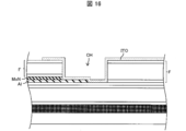
- FIG. 10 is a cross-sectional view showing another configuration of the active matrix substrate according to the fourth embodiment. It is sectional drawing which shows the structure of the active matrix substrate which concerns on a reference form.
- Embodiment 1 the MEMS display 80 according to the first embodiment includes an optical shutter substrate 20 and an optical shutter device 60 including a counter substrate 30 facing the optical shutter substrate 20, and an optical shutter substrate via the counter substrate 30.
- 20 includes a backlight BL that irradiates LED light or laser light.
- the optical shutter substrate 20 is arranged on an active matrix substrate 17 including thin film transistors (TFTs) and a plurality of micro electro mechanical systems (MEMS) that are disposed on the backlight BL side of the active matrix substrate 17.
- An optical shutter mechanism 21 is provided.
- the optical shutter mechanism 21 is provided for each pixel, and the optical shutter substrate 20 is provided with a light transmission path through which light that has passed through the optical shutter mechanism 21 passes.
- the optical shutter mechanism 21 includes a shutter body 28 having an opening 28k, a shutter beam 23x connected to one side end of the shutter body 28, a shutter beam 23y connected to the other side end, and a shutter.
- a drive beam 22x facing the beam 23x and a drive beam 22y facing the shutter beam 23y are included.
- the shutter beam 23x is connected to the shutter line of the active matrix layer via the shutter anchor 23b
- the shutter beam 23y is connected to the shutter line of the active matrix layer via the shutter anchor 23d
- the drive beam 22x is connected to the shutter anchor 22b.
- the drive beam 22y is connected to another TFT of the active matrix layer via a drive anchor 22d, and the spring-like shutter beams 23x and 23y are controlled by controlling the potential of the drive beams 22x and 22y.
- the shutter body 28 is deformed and slides in a direction parallel to the substrate surface. Accordingly, the amount of light emitted to the viewer 50 through the optical shutter mechanism and the light transmission path is controlled, and an image is displayed.
- FIG. 3 is a circuit diagram showing a configuration of a part of the optical shutter substrate 20.
- the optical shutter substrate includes seven signal lines including a scanning line SC, a data line DS, an actuate line AC, an update line UD, a shutter line ST, a precharge line PC, and an enable line EN.
- Transistors TR1 to TR5, a data holding capacitor C1, a master capacitor C2, and a slave capacitor C3 are provided.
- the voltage from the actuate line AC is applied to the drive beam 22x connected to the master capacitor C2 and the drive beam 22y connected to the slave capacitor C3 via the transistors TR1 and TR2. Stored.
- TR4 is controlled according to the data voltage. Specifically, when the data voltage is high, the transistor TR4 is turned on, and when the data voltage is low, the transistor TR4 remains off.
- the transistor TR5 is controlled according to the voltage of the drive beam 22x. Specifically, when the data voltage is Low and the driving beam 22x is High, the transistor TR5 is turned on. When the data voltage is High and the driving beam 22x is Low, the transistor TR5 is turned off.
- the drive beam 22x and the drive beam 22y have opposite polarities, and the drive beam (22x or 22y) having the opposite polarity to the shutter body 28 attracts the shutter body 28 by electrical force.
- the shutter body 28 is supplied with a signal whose polarity is periodically reversed from the shutter line ST to prevent charging.
- the optical shutter mechanism 21 when the shutter body 28 is drawn toward the drive beam 22y, the optical shutter mechanism 21 is in an open state (FIG. 1B and FIG. 2). a)), when the shutter body 28 is drawn toward the drive beam 22x, the optical shutter mechanism 21 is closed (see FIG. 1C and FIG. 2B).
- a counter substrate 30 formed by forming a light shielding layer 32 of metal or the like on a glass substrate 31 is provided between the optical shutter substrate 20 and the backlight BL, and the light shielding layer of the counter substrate 30 is provided.
- a light transmission path LW is formed from the slit 32s formed in 32 to the slit 2s of the light shielding film 2 of the optical shutter substrate 20 in a direction perpendicular to the substrate surface, as shown in FIG.
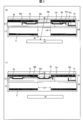
- FIG. 4A is a cross-sectional view of a TFT (thin film transistor) portion in the active matrix substrate of Embodiment 1
- FIG. 4B is a perspective plan view corresponding to FIG.
- FIG. 5A is a cross-sectional view of a contact portion of a metal film in the active matrix substrate of Embodiment 1
- FIG. 5B is a perspective plan view corresponding to FIG.
- the TFT portion has a channel etch structure.
- the active matrix substrate 17 includes a glass substrate 1, a light shielding film 2 formed on the glass substrate 1, and a first inorganic insulating film 3 a formed on the light shielding film 2.
- the lower metal film 5 formed, the gate insulating film 6 formed on the upper layer of the lower metal film 5, and the oxide semiconductor film 7s and the oxide semiconductor film formed on the upper layer of the gate insulating film 6 are obtained as conductors.
- the conductive film 7c is a conductive oxide semiconductor film, and has a state of an oxide semiconductor film that functions as a conductor with lower resistance than an oxide semiconductor film that functions as a channel of a transistor.
- the light-shielding film 2 uses a light-shielding resin (for example, spin-on glass material) that can be applied, and the lower light-transmitting film 4 and the upper light-transmitting film 11 use a light-transmitting resin (for example, spin-on glass material) that can be applied. Is formed.
- the light shielding film 2, the lower light transmissive film 4 and the upper light transmissive film 11 have a thickness of 0.5 to 3 ⁇ m, which is larger than the thickness of the lower metal film 5 and the first metal film 9, respectively. Function.
- the first and second inorganic insulating films 3a and 3b are provided to improve the adhesion between the lower layer film and the upper layer film.
- the thickness is about 50 to 200 nm, and for example, SiO 2 is used as the material.
- the gate insulating film 6 is formed by sequentially forming a SiNx film and a SiO 2 film by a PECVD method. However, a single layer film such as a SiO 2 film or a SiNx film may be used.
- the oxide semiconductor film for obtaining the oxide semiconductor film 7s and the conductive film 7c is formed by patterning an oxide semiconductor film formed by a sputtering method.
- An oxide semiconductor has an electron mobility 20 to 50 times that of amorphous silicon, which is an amorphous semiconductor, and enables high-speed switching of a transistor on an optical shutter substrate, and thus high-speed opening and closing of the shutter body 28 in the optical shutter mechanism.
- This oxide semiconductor may contain at least one metal element of In, Ga, and Zn.
- an In—Ga—Zn—O-based semiconductor eg, indium gallium zinc oxide
- the In—Ga—Zn—O-based semiconductor is a ternary oxide of In (indium), Ga (gallium), and Zn (zinc).
- an In—Sn—Zn—O-based semiconductor eg, In 2 O 3 —SnO 2 —ZnO; InSnZnO
- the In—Sn—Zn—O-based semiconductor is a ternary oxide of In (indium), Sn (tin), and Zn (zinc).
- Al is aluminum
- Ti is titanium
- Cd is cadmium
- Ge germanium
- Pb is lead
- Mg magnesium
- Zr zirconium
- Hf hafnium.
- the first to third passivation films 10a to 10c are formed by sequentially forming and patterning a SiNx film and a SiO 2 film by a PECVD method.
- a single layer film such as a SiO 2 film or a SiNx film may be used.
- an aluminum (Al) film, a tungsten (W) film, a molybdenum (Mo) film, a tantalum (Ta) film, a chromium (Cr) film, and a titanium (Ti) film In addition, a metal such as copper (Cu) or an alloy thereof is formed into a single layer or a plurality of layers by sputtering and patterned.
- the first metal film 9 is a laminated film composed of a lower film 9x (for example, aluminum) and an upper film 9y (for example, molybdenum nitride).
- ITO Indium ⁇ Tin ⁇ Oxide
- IZO Indium Zincum Oxide
- Cu copper
- a material that causes electrolytic corrosion by contact is used for the first and second metal films.
- Al is used for the first metal film 9, and ITO is used for the second metal film 12.
- the present invention is not limited to this.
- Al is used for the first metal film 9, and Cu is used for the second metal film 12. It can also be used.
- the lower metal film 5, the gate insulating film 6, the oxide semiconductor film 7s, and the first metal films 9s and 9d constitute a TFT (for example, the transistor TR4 in FIG. 2).
- the first metal film 9d and the second metal film 12 are in contact with each other in a contact hole provided in the interlayer insulating film F composed of the first passivation film 10a, the upper light-transmitting film 11, and the second passivation film 10b. Both are electrically connected.
- An upper metal film 13 is formed on the second metal film 12 so as to be in contact therewith.
- a conductive film 7 c obtained by making an oxide semiconductor film a conductor is formed immediately below the contact hole CH provided in the interlayer insulating film F, and the peripheral end of the conductive film 7 c is formed in the contact hole CH. Located outside. That is, the conductive film 7c overlaps the entire inner region of the contact hole CH.
- the conductive film 7c in FIG. 5 is subjected to plasma treatment on the oxide semiconductor film formed in the same layer (in the same step) as the oxide semiconductor film 7s (see FIG. 4) functioning as a TFT channel, thereby converting the oxide semiconductor film into a conductor. It was obtained.
- the conductive film 7c (the overlapping portion overlapping the contact hole) and the second metal film 12 are in contact with each other, and both are electrically connected.
- the first metal film 9 (laminated film of the lower film 9x and the upper film 9y) is formed so as not to overlap with the contact hole CH, and on the outer side of the bottom of the contact hole CH, the peripheral end portion of the conductive film 7c.
- the non-overlapping portion that does not overlap the contact hole and the end portion 9E of the first metal film 9 (end portion of the lower film 9x) are in contact with each other and are electrically connected.
- an interlayer insulating film F is formed between the sidewall CW of the contact hole CH and the end face 9F of the first metal film 9, and the distance between the sidewall CW of the contact hole CH and the end face 9F of the first metal film 9 is formed.
- d is designed to be smaller than the thickness D of the interlayer insulating film F (within about 2 ⁇ m).
- FIG. 6 is a flowchart showing a part of the manufacturing process of the active matrix substrate.
- step S1 the light shielding film 2 is formed and patterned, and in step S2, the lower transparent film 4 is formed and patterned.
- step S3 the lower metal film 5 is formed and patterned, and in step S4, a gate insulating film is formed.
- step S5 an oxide semiconductor film is formed, and in step S6, high-temperature annealing is performed.
- the high-temperature annealing treatment is performed, for example, under a nitrogen atmosphere at 400 to 500 ° C. for 1 to 2 hours.
- step S7 the oxide semiconductor film is patterned.
- the oxide semiconductor film is left in the channel region of the TFT in FIG. 4 and the contact region CR (see FIG. 5B) corresponding to the contact hole CH in FIG.
- the oxide semiconductor film is left wider than the contact region CR so as to include the contact region CR, and the peripheral end portion of the oxide semiconductor film protrudes from the contact region CR.
- a first metal film 9 (for example, a laminated film of a lower film 9x made of Al and an upper film 9y made of MoN) is formed and patterned.
- the end 9E of the first metal film 9 in FIG. 5 is overlapped with the peripheral end of the oxide semiconductor film (the part protruding from the contact region CR) (the lower film 9x (Al) is formed on the oxide semiconductor film).
- the end surface 9F of the first metal film 9 is disposed outside the contact region CR.
- step S9 the first passivation film 10a is formed, in step S10, the upper light-transmitting film 11 is formed, and in step S11, the second passivation film 10b is formed.
- step S12 the interlayer insulating film (the first passivation film 10a, the upper light-transmitting film 11, and the second passivation film 10b) is patterned.
- the contact hole CH is formed in the interlayer insulating film F on the contact region CR, and the oxide semiconductor film is exposed at the bottom thereof.
- step S13 the oxide semiconductor film overlapping the contact region CR is subjected to plasma treatment using oxygen (Ar, Ar, hydrogen (H), or the like).
- the oxide semiconductor film overlapping the contact region CR has a portion overlapping the end portion 9E of the first metal film 9 in addition to the portion exposed at the bottom of the contact hole CH, and the contact hole CH from this portion.
- a portion up to the side wall portion on which the interlayer insulating film F is formed on the upper side
- the distance d between the sidewall CW of the contact hole CH and the end face 9F of the first metal film 9 is smaller than the thickness D of the interlayer insulating film F, the oxide semiconductor functioning as a channel in step S13.
- the film up to 7s is prevented from being made into a conductor.
- step S14 the second metal film 12 is formed on the interlayer insulating film F.
- the conductive film 7c and the second metal film 12 are in contact with each other at the bottom of the contact hole CH and are electrically connected.
- the first metal film 9 and the second metal film 12 are electrically connected via the conductive film 7c.
- the active matrix substrate 17 shown in FIG. 5 can be formed.
- the interlayer insulating film is contacted as shown in FIG.
- the upper film (MoN) of the first metal film is etched in the etching process for forming the hole CH, and the lower film (Al) of the first metal film and the ITO (second metal film) are in contact with each other in the contact hole.
- electrical corrosion occurs between the two, resulting in contact failure.
- FIGS. 5A and 5B In the second embodiment, the configuration shown in FIGS. 5A and 5B is configured as shown in FIGS. 7A and 7B.
- the conductive film 7c (the overlapping portion overlapping the contact hole) and the second metal film 12 are in contact with each other, and both are electrically connected.
- the conductive film 7c in FIG. 7 is obtained by subjecting a semiconductor film formed in the same layer (in the same process) as the oxide semiconductor film 7s in FIG.
- the peripheral end portion (non-overlapping portion that does not overlap the contact hole) of the conductive film 7c and the end portion 9E of the first metal film 9 are in contact with each other and are electrically connected.
- the interlayer insulating film F is not formed between the end surface 9F of the first metal film and the second metal film 12 in the contact hole CH, which is a cavity.
- Step S7 can be formed as shown in FIG. Steps S1 to S7 are the same as in FIG. 6.
- a first metal film 9 for example, a laminated film of a lower film 9x made of Al and an upper film 9y made of MoN is formed and patterned.
- the end portion 9e of the first metal film 9 is overlaid on the peripheral end portion (the portion protruding from the contact region CR) of the oxide semiconductor film 7s, and the first metal film 9
- the end face 9f is arranged on the edge of the contact region CR or inside thereof.
- step S9 the first passivation film 10a is formed, in step S10, the upper light-transmitting film 11 is formed, and in step S11, the second passivation film 10b is formed.
- step S12 an interlayer insulating film F is formed and patterned. At this time, a contact hole CH is formed in the interlayer insulating film F on the contact region CR, and the oxide semiconductor film 7s is exposed at the bottom thereof.
- step S13 wet etching of the first metal film 9 (9x / 9y) is performed, and the end surface 9F of the first metal film 9 is separated from the edge (side wall position) of the contact region CR as shown in FIG. 9B.
- the end surface 9F of the first metal film 9 is positioned outside the contact region CR, and the end portion 9E of the first metal film 9 overlaps the oxide semiconductor film 7s (the lower film 9x is the oxide semiconductor film). 7s).
- step S14 plasma treatment using, for example, argon or hydrogen other than oxygen is performed on the oxide semiconductor film 7s in the contact region CR.
- the oxide semiconductor film 7s that overlaps the contact region CR has a portion that overlaps the end 9E of the first metal film 9 in addition to the portion exposed at the bottom of the contact hole CH, and the contact hole CH from this portion.
- the portion up to the bottom (the portion where the interlayer insulating film F is not formed on the upper side) is made into a conductive film 7c, and the conductive film 7c and the first metal film 9 (lower film 9x) are electrically connected. Connected.
- the interlayer insulating film F does not exist (is a cavity) in the gap from the end face 9F of the first metal film 9 to the edge (side wall position) of the contact hole CH, the oxide semiconductor film below this gap Is easily made into a conductor by plasma treatment. Therefore, this gap can be made larger than the thickness of the interlayer insulating film F, and the alignment of the oxide semiconductor film 7s in step S7 is facilitated.
- step S15 the second metal film 12 is formed on the interlayer insulating film F.
- the conductive film 7c and the second metal film 12 are in contact with each other at the bottom of the contact hole CH and are electrically connected.
- the first metal film 9 and the second metal film 12 are electrically connected via the conductive film 7c.
- the active matrix substrate 17 of FIG. 7 can be formed.
- the second metal film 12 is disconnected at the side wall portion of the contact hole CH, but the conduction with the conductive film 7c is ensured at the surrounding portion.
- the TFT portion is configured as a channel etch type, but the present invention is not limited to this.
- the configuration in which the etching stopper film 8 is provided as shown in FIG. 10 is also a function. Specifically, the etching stopper film 8 is formed on the oxide semiconductor film 7 s, and the first metal films 9 s and 9 d are formed on the etching stopper film 8.
- the etching stopper film 8 is formed, for example, by forming a SiO 2 film by PECVD and patterning.
- the etching stopper film 8 By providing the etching stopper film 8, it is possible to prevent the oxide semiconductor film 7s from being affected by the etching of the first metal film when the first metal films 9s and 9d are formed.
- the contact hole CH is provided in the interlayer insulating film F on the upper layer of the conductive film 7c obtained by making the oxide semiconductor film into a conductor, and the conductive film is formed inside the contact hole CH.
- 7c and the second metal film 12 are in contact with each other, and the conductive film 7c and the first metal film 9 (for example, the lower film 9x made of Al and MoN are formed outside the contact hole CH.
- the interlayer insulating film F may be formed in the gap from the end face 9F of the first metal film 9 to the second metal film 12 in the contact hole CH. As shown in FIG. The interlayer insulating film F may not be present (void) in the gap from the end face 9F of the first metal film 9 to the second metal film 12 in the contact hole CH.
- Embodiment 4 Although the MEMS display has been described in the first embodiment, the present invention is not limited to this.
- the active matrix substrates of Embodiments 1 to 3 can also be applied to liquid crystal display devices.
- the liquid crystal display device 100 of Embodiment 4 includes a liquid crystal panel 67 including an active matrix substrate 27 and a counter substrate (color filter substrate) 37, and LED light and laser light on the active matrix substrate 27. And a backlight BL that emits light.
- the pixel electrode of the liquid crystal capacitor LC is connected to the data signal line DS and the scanning signal line SC through the transistor Tr, and the counter electrode of the liquid crystal capacitor LC is It is connected to the common electrode line COM.
- the liquid crystal panel 67 includes the light shielding film 2, the first inorganic insulating film 3 a, the lower light transmissive film 4, the first light transmitting film 4, from the size active matrix substrate 17 of the first embodiment shown in FIGS. 2
- An active matrix substrate 27 in which the inorganic insulating film 3b and the third passivation film 10c are omitted can be used.
- FIG. 15 from the active matrix substrate 17 of the second embodiment shown in FIGS. 4 and 7, the light shielding film 2, the first inorganic insulating film 3a, the lower transparent film 4, and the second inorganic insulating film.
- An active matrix substrate 27 from which 3b and the third passivation film 10c are omitted can also be used.
- an active matrix substrate according to one embodiment of the present invention is an active matrix substrate having a structure in which two metal films formed in different layers are electrically connected to each other (particularly, when there is a risk of electrical corrosion due to contact between these metal films) ).
- An organic EL (organic electroluminescence) display and an inorganic EL (inorganic electroluminescence) display are also suitable.
- An active matrix substrate includes a substrate, a first metal film, an interlayer insulating film formed above the first metal film, and a second layer formed above the interlayer insulating film.
- the active matrix substrate according to aspect 2 of the present invention is the structure according to aspect 2, wherein the first metal film does not overlap the contact hole.
- the conductive oxide semiconductor film overlaps the entire inner region of the contact hole.
- the active matrix substrate according to aspect 4 of the present invention is the active matrix substrate according to aspect 2, in which the end portion of the first metal film has an end surface that faces the side wall of the contact hole, and extends from the end surface to the side wall of the contact hole. The distance is smaller than the thickness of the interlayer insulating film.
- the active matrix substrate according to aspect 5 of the present invention is the active matrix substrate according to aspect 2, wherein the end of the first metal film is located away from the contact hole, the end of the first metal wiring, and the contact hole A cavity is formed between the second metal film and the second metal film.
- the second metal film is a translucent metal film.
- the active matrix substrate according to aspect 7 of the present invention is the active matrix substrate according to any one of the aspects 1 to 6, wherein the conductive oxide semiconductor film is formed in the same layer as the oxide semiconductor film functioning as a channel of the transistor. It is the structure which is the made electrically conductive film.
- the first metal film includes aluminum.
- An optical shutter substrate according to aspect 9 of the present invention includes the active matrix substrate according to any one of aspects 1 to 7 and an optical shutter mechanism formed on the active matrix substrate.
- a display device includes the active matrix substrate according to any one of aspects 1 to 7.
- An active matrix substrate manufacturing method includes a first step of forming an oxide semiconductor film, a second step of forming a first metal film on the oxide semiconductor film, and the first step.
- the method includes a fifth step of using the oxide semiconductor film as a conductive film, and a sixth step of forming a second metal film so as to cover the conductive film inside the contact hole.
- the method of manufacturing an active matrix substrate according to aspect 12 of the present invention is the method of manufacturing the active matrix substrate according to aspect 11, in the second step, wherein the second step does not overlap with the formation position of the contact hole and contacts the oxide semiconductor film. This is a technique for forming one metal film.
- the first metal film is overlapped with the contact hole forming position and is in contact with the oxide semiconductor film.
- the first metal film is in contact with the oxide semiconductor film but is not overlapped with the contact hole during the fourth and fifth steps.
Landscapes
- Physics & Mathematics (AREA)
- General Physics & Mathematics (AREA)
- Nonlinear Science (AREA)
- Engineering & Computer Science (AREA)
- Optics & Photonics (AREA)
- Microelectronics & Electronic Packaging (AREA)
- Mathematical Physics (AREA)
- Chemical & Material Sciences (AREA)
- Crystallography & Structural Chemistry (AREA)
- Theoretical Computer Science (AREA)
- Thin Film Transistor (AREA)
- Devices For Indicating Variable Information By Combining Individual Elements (AREA)
Abstract
2つの導体膜間のコンタクト不良が生じにくいアクティブマトリクス基板を提供する。基板(1)と第1金属膜(9)との間の層に、導体化された酸化物半導体膜(7c)が設けられ、コンタクトホール(CH)の内部で、導体化された酸化物半導体膜(7c)と第2金属膜(12)とが接触し、コンタクトホール(CH)の外部で、導体化された酸化物半導体膜(7c)と第1金属膜(9)とが接触している。
Description
本発明は、表示装置に用いるアクティブマトリクス基板に関する。
液晶表示装置、有機EL表示装置、MEMS(Micro Electro Mechanical Systems)ディスプレイ等の表示装置には、複数のTFT(薄膜トランジスタ)が並べられたアクティブマトリクス基板が用いられる。
アクティブマトリクス基板は、一般に、異なる層に形成された2つの導体膜をコンタクトホールを介して接続する構造を含んでいるが、コンタクトホール内で生じる2つの導体膜間の電触によって両者間のコンタクト不良が生じうる。
本発明の目的の1つは、2つの導体膜間のコンタクト不良が生じにくいアクティブマトリクス基板を提供することにある。
本発明の一態様に係るアクティブマトリクス基板は、基板と、第1金属膜と、前記第1金属膜よりも上層に形成された層間絶縁膜と、層間絶縁膜よりも上層に形成された第2金属膜とを備え、前記層間絶縁膜に形成されたコンタクトホールを介して第1および第2金属膜が電気的に接続されているアクティブマトリクス基板であって、前記基板と前記第1金属膜との間の層に、導体化された酸化物半導体膜が設けられ、前記コンタクトホールの内部で前記導体化された酸化物半導体膜と前記第2金属膜とが接触し、前記コンタクトホールの外部で前記導体化された酸化物半導体膜と前記第1金属膜とが接触している構成である。
なお、導体化された酸化物半導体膜とは、トランジスタのチャネルとして機能する酸化物半導体膜とは異なり、導体として機能する酸化物半導体膜であり、酸化物半導体膜が低抵抗である状態を示す。
前記構成によれば、2つの導体膜間のコンタクト不良が生じにくいアクティブマトリクス基板を実現することができる。
図1~図16に基づき、以下に本発明の実施形態を説明する。
〔実施形態1〕
(MEMSディスプレイ)
図1に示すように、実施の形態1にかかるMEMSディスプレイ80は、光シャッタ基板20および光シャッタ基板20に対向する対向基板30を含む光シャッタ装置60と、対向基板30を介して光シャッタ基板20にLED光やレーザ光を照射するバックライトBLとを備える。
(MEMSディスプレイ)
図1に示すように、実施の形態1にかかるMEMSディスプレイ80は、光シャッタ基板20および光シャッタ基板20に対向する対向基板30を含む光シャッタ装置60と、対向基板30を介して光シャッタ基板20にLED光やレーザ光を照射するバックライトBLとを備える。
(光シャッタ基板の構成)
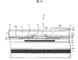
図2に示すように、光シャッタ基板20は、薄膜トランジスタ(TFT)を含むアクティブマトリクス基板17と、このアクティブマトリクス基板17のバックライトBL側に配され、MEMS(Micro Electro Mechanical Systems)である複数の光シャッタ機構21を備える。光シャッタ機構21は、画素ごとに設けられ、光シャッタ基板20には、光シャッタ機構21を通過した光が通る光透過経路が設けられる。
図2に示すように、光シャッタ基板20は、薄膜トランジスタ(TFT)を含むアクティブマトリクス基板17と、このアクティブマトリクス基板17のバックライトBL側に配され、MEMS(Micro Electro Mechanical Systems)である複数の光シャッタ機構21を備える。光シャッタ機構21は、画素ごとに設けられ、光シャッタ基板20には、光シャッタ機構21を通過した光が通る光透過経路が設けられる。
光シャッタ機構21は、図1に示すように、開口28kを有するシャッタ体28と、シャッタ体28の一側端に接続するシャッタビーム23xと、他の側端に接続するシャッタビーム23yと、シャッタビーム23xと向かい合う駆動ビーム22xと、シャッタビーム23yと向かい合う駆動ビーム22yとを含む。
シャッタビーム23xはシャッタアンカー23bを介してアクティブマトリクス層のシャッタ線に接続され、シャッタビーム23yはシャッタアンカー23dを介してアクティブマトリクス層のシャッタ線に接続され、駆動ビーム22xは駆動アンカー22bを介してアクティブマトリクス層のTFTに接続され、駆動ビーム22yは駆動アンカー22dを介してアクティブマトリクス層の別のTFTに接続されており、駆動ビーム22x・22yの電位制御によってバネ状のシャッタビーム23x・23yが変形し、シャッタ体28が基板面に平行な方向にスライドする。これにより、光シャッタ機構および光透過経路を通って視認者50に出射される光の光量が制御され、画像が表示される。
図3は光シャッタ基板20の一部の構成を示す回路図である。図3に示すように、光シャッタ基板は、走査線SC、データ線DS、アクチュエート線AC、アップデート線UD、シャッタ線ST、プリチャージ線PC、およびイネーブル線ENの7本の信号線と、トランジスタTR1~TR5と、データ保持容量C1並びにマスタ容量C2およびスレーブ容量C3とを備える。
図3の構成では、走査線SCが選択されると、光シャッタ機構の開閉を決めるデータ電圧が、データ線DSおよびトランジスタTR3を介して、データ保持容量C1に蓄えられる。この期間は、アップデート線UDをHighとし、トランジスタTR4をデータ電圧によらずオフとしている。
次いでプリチャージ線PCが選択されると、アクチュエート線ACからの電圧が、トランジスタTR1およびTR2を介して、マスタ容量C2に接続する駆動ビーム22xと、スレーブ容量C3に接続する駆動ビーム22yとに蓄えられる。
次いでアップデート線UDがHighからLowに変化するとデータ電圧に応じてTR4が制御される。具体的には、データ電圧がHighの場合はトランジスタTR4はオンし、データ電圧がLowの場合はトランジスタTR4はオフのままとなる。
次いでイネーブル線ENがHighからLowに変化すると、駆動ビーム22xの電圧に応じてトランジスタTR5が制御される。具体的には、データ電圧がLowで駆動ビーム22xがHighのときはトランジスタTR5がオンし、データ電圧がHighで駆動ビーム22xがLowであれば、トランジスタTR5はオフする。
このように駆動ビーム22xと駆動ビーム22yとは互いに逆極性となり、シャッタ体28の極性と逆極性となる駆動ビーム(22xあるいは22y)が電気的な力によってシャッタ体28を引き寄せる。なお、シャッタ体28には、帯電防止のため、シャッタ線STから周期的に極性が反転する信号が供給されている。
図1および図2に示すように、光シャッタ機構21では、シャッタ体28が駆動ビーム22y側に引き寄せられると、光シャッタ機構21が開(オープン)状態となり(図1(b)および図2(a)参照)、シャッタ体28が駆動ビーム22x側に引き寄せられると、光シャッタ機構21が閉(クローズ)状態となる(図1(c)および図2(b)参照)。
図2の光シャッタ装置では、光シャッタ基板20とバックライトBLとの間に、ガラス基板31上に金属等の遮光層32を形成してなる対向基板30が設けられ、対向基板30の遮光層32に形成されたスリット32sから、基板面に垂直な方向に向かって、光シャッタ基板20の遮光膜2のスリット2sに至る、光透過経路LWが形成されており、図2(a)のようにシャッタ体28の開口28kが光透過経路LWと重なる(光シャッタ機構がオープン状態の)ときにバックライト光は光シャッタ機構21および光透過経路LWを通って視認者50側に出射され、図2(b)のようにシャッタ体28の開口以外の部分が光透過経路LWと重なる(光シャッタ機構21がクローズ状態の)ときにバックライト光は遮断される。
(アクティブマトリクス基板の構成)
図4(a)は、実施形態1のアクティブマトリクス基板におけるTFT(薄膜トランジスタ)部分の断面図であり、図4(b)は、図4(a)に対応する透視平面図である。図5(a)は、実施形態1のアクティブマトリクス基板における金属膜のコンタクト部分の断面図であり、図5(b)は、図5(a)に対応する透視平面図である。なお、実施形態1ではTFT部分をチャネルエッチ構造としている。
図4(a)は、実施形態1のアクティブマトリクス基板におけるTFT(薄膜トランジスタ)部分の断面図であり、図4(b)は、図4(a)に対応する透視平面図である。図5(a)は、実施形態1のアクティブマトリクス基板における金属膜のコンタクト部分の断面図であり、図5(b)は、図5(a)に対応する透視平面図である。なお、実施形態1ではTFT部分をチャネルエッチ構造としている。
図4および図5に示すように、アクティブマトリクス基板17は、ガラス基板1と、ガラス基板1の上層に形成された遮光膜2と、遮光膜2の上層に形成された第1無機絶縁膜3aと、第1無機絶縁膜3aの上層に形成された下層透光膜4と、下層透光膜4の上層に形成された第2無機絶縁膜3bと、第2無機絶縁膜3bの上層に形成された下層金属膜5と、下層金属膜5の上層に形成されたゲート絶縁膜6と、ゲート絶縁膜6の上層に形成された、酸化物半導体膜7sおよび酸化物半導体膜を導体化して得られる導電膜7cと、酸化物半導体膜7sおよび導電膜7cの上層に形成された第1金属膜9(9s・9d)と、第1金属膜9の上層に形成された第1パッシベーション膜10と、第1パッシベーション膜10の上層に形成された上層透光膜11と、上層透光膜11の上層に形成された第2パッシベーション膜10bと、第2パッシベーション膜10bの上層に形成された第2金属膜12と、第2金属膜12の上層に形成された上層金属膜13と、上層金属膜13の上層に形成された第3パッシベーション膜10cとを備える。
導電膜7cは導体化された酸化物半導体膜であり、トランジスタのチャネルとして機能する酸化物半導体膜よりも低抵抗で、導体として機能する酸化物半導体膜の状態を有している。
遮光膜2は塗布可能な遮光性樹脂(例えば、スピンオンガラス材料)を用いて、下層透光膜4および上層透光膜11は塗布可能な透光性樹脂(例えば、スピンオンガラス材料)を用いて形成されている。これら遮光膜2、下層透光膜4および上層透光膜11はそれぞれ、下層金属膜5および第1金属膜9の厚みよりも大きい0.5~3μmの厚みを有し、平坦化膜としても機能する。
第1および第2無機絶縁膜3a・3bは、その下層膜および上層膜の密着性を高めるために設けられる。その厚みは50~200nm程度であり、材料には、例えばSiO2を用いる。
ゲート絶縁膜6は、SiNx膜およびSiO2膜を順次PECVD法で成膜して形成される。もっとも、SiO2膜やSiNx膜の単層膜でもよい。
酸化物半導体膜7sおよび導電膜7cを得るための酸化物半導体膜は、スパッタ法を用いて成膜した酸化物半導体膜をパターニングすることで形成される。酸化物半導体は、非晶質半導体のアモルファスシリコンに比べて20~50倍の電子移動度を有し、光シャッタ基板のトランジスタの高速スイッチング、ひいては、光シャッタ機構におけるシャッタ体28の高速開閉を可能とする。
この酸化物半導体は、In、GaおよびZnのうち少なくとも1種の金属元素を含んでいてもよい。例えば、In-Ga-Zn-O系の半導体(例えば、インジウムガリウム亜鉛酸化物)を挙げることができる。In-Ga-Zn-O系の半導体は、In(インジウム)、Ga(ガリウム)、Zn(亜鉛)の三元系酸化物である。In、GaおよびZnの割合(組成比)は特に限定されず、例えばIn:Ga:Zn=2:2:1、In:Ga:Zn=1:1:1、In:Ga:Zn=1:1:2などでも良い。
また、In-Sn-Zn-O系半導体(例えばIn2O3-SnO2-ZnO;InSnZnO)でもよい。In-Sn-Zn-O系半導体は、In(インジウム)、Sn(スズ)およびZn(亜鉛)の三元系酸化物である。
また、In-Al-Zn-O系半導体、In-Al-Sn-Zn-O系半導体、Zn-O系半導体、In-Zn-O系半導体、Zn-Ti-O系半導体、Cd-Ge-O系半導体、Cd-Pb-O系半導体、CdO(酸化カドミウム)、Mg-Zn-O系半導体、In-Ga-Sn-O系半導体、In-Ga-O系半導体、Zr-In-Zn-O系半導体、Hf-In-Zn-O系半導体などでもよい。なお、Alはアルミニウム、Tiはチタン、Cdはカドミウム、Geはゲルマニウム、Pbは鉛、Mgはマグネシウム、Zrはジルコニウム、Hfはハフニウムを表す。
第1~第3パッシベーション膜10a~10cは、SiNx膜およびSiO2膜を順次PECVD法で成膜し、パターニングすることで形成される。もっとも、SiO2膜やSiNx膜の単層膜でもよい。
下層金属膜、第1金属膜、上層金属膜については、アルミニウム(Al)膜、タングステン(W)膜、モリブデン(Mo)膜、タンタル(Ta)膜、クロム(Cr)膜、チタン(Ti)膜、銅(Cu)等の金属あるいはこれらの合金を、スパッタ法によって単層または複層に成膜し、パターニングすることで形成される。
実施形態1では、第1金属膜9を、下側膜9x(例えば、アルミニウム)および上側膜9y(例えば、窒化モリブデン)からなる積層膜としている。
第2金属膜12には、透光金属膜であるITO(Indium Tin Oxide)あるいはIZO(Indium Zincum Oxide)や、銅(Cu)を用いることができる。
本実施形態では、第1および第2金属膜に、接触によって電蝕が起こる材料を用いている。具体的には、第1金属膜9にAl、第2金属膜12にITOを用いているが、これに限定されず、例えば、第1金属膜9にAl、第2金属膜12にCuを用いることもできる。
光シャッタ機構については、n+アモルファスシリコンと、アルミニウム(Al)膜、タングステン(W)膜、モリブデン(Mo)膜、タンタル(Ta)膜、クロム(Cr)膜、チタン(Ti)膜、銅(Cu)等の金属あるいはこれらの合金と、SiNxとを用い、フォトリソグラフィ工程およびエッチング工程等を用いて形成される。
図4では、下層金属膜5、ゲート絶縁膜6、酸化物半導体膜7s、および第1金属膜9s・9dによってTFT(例えば、図2のトランジスタTR4)が構成されている。また、第1パッシベーション膜10a、上層透光膜11および第2パッシベーション膜10bからなる層間絶縁膜Fに設けられたコンタクトホール内で、第1金属膜9dと第2金属膜12とが接触し、両者が電気的に接続されている。なお、第2金属膜12上には、これと接するように上層金属膜13が形成されている。
図5では、層間絶縁膜Fに設けられたコンタクトホールCHの直下に、酸化物半導体膜を導体化して得られる導電膜7cが形成されており、導電膜7cの周端部はコンタクトホールCHの外側に位置する。すなわち、導電膜7cは、コンタクトホールCHの内側領域の全体と重なる。図5の導電膜7cは、TFTのチャネルとして機能する酸化物半導体膜7s(図4参照)と同層に(同工程で)形成された酸化物半導体膜にプラズマ処理を施し、これを導体化して得られたものである。
そして、コンタクトホールCHのボトムにおいて、導電膜7c(コンタクトホールに重なる重畳部)と第2金属膜12とが接触し、両者が電気的に接続されている。
さらに、第1金属膜9(下側膜9xおよ上側膜9yの積層膜)が、コンタクトホールCHと重畳しないように形成され、コンタクトホールCHのボトムの外側では、導電膜7cの周端部(コンタクトホールに重ならない非重畳部)と、第1金属膜9の端部9E(下側膜9xの端部)とが接触し、電気的に接続されている。ここでは、コンタクトホールCHの側壁CWと第1金属膜9の端面9Fとの間に層間絶縁膜Fが形成され、コンタクトホールCHの側壁CWと第1金属膜9の端面9Fとの間の距離dは、層間絶縁膜Fの厚みDよりも小さく(2μm程度以内に)設計されている。
(アクティブマトリクス基板の製造方法)
図6は、アクティブマトリクス基板の製造工程の一部を示すフローチャートである。ステップS1では、遮光膜2を成膜およびパターニングし、ステップS2では、下層透光膜4を成膜およびパターニングする。ステップS3では、下層金属膜5を成膜およびパターニングし、ステップS4では、ゲート絶縁膜を成膜する。
図6は、アクティブマトリクス基板の製造工程の一部を示すフローチャートである。ステップS1では、遮光膜2を成膜およびパターニングし、ステップS2では、下層透光膜4を成膜およびパターニングする。ステップS3では、下層金属膜5を成膜およびパターニングし、ステップS4では、ゲート絶縁膜を成膜する。
ステップS5では、酸化物半導体膜を成膜し、ステップS6で高温アニール処理を行う。高温アニール処理は、例えば、窒素雰囲気下、400~500℃、1~2時間の条件で行う。
ステップS7では、酸化物半導体膜をパターニングする。このとき、図4のTFTのチャネル領域と、図5のコンタクトホールCHに該当するコンタクト領域CR(図5(b)参照)とに、酸化物半導体膜を残しておく。具体的には、コンタクト領域CRを包含するように、酸化物半導体膜をコンタクト領域CRよりも広く残し、酸化物半導体膜の周端部がコンタクト領域CRからはみ出るようにする。
ステップS8では第1金属膜9(例えば、Alからなる下側膜9xおよびMoNからなる上側膜9yの積層膜)を成膜およびパターニングする。このとき、図5の第1金属膜9の端部9Eを、酸化物半導体膜の周端部(コンタクト領域CRからはみ出た部分)に重ね(下側膜9x(Al)を酸化物半導体膜に接触させ)、第1金属膜9の端面9Fをコンタクト領域CRの外側に配する。
ステップS9では第1パッシベーション膜10aを成膜し、ステップS10では上層透光膜11を成膜し、ステップS11では第2パッシベーション膜10bを成膜する。
ステップS12では、層間絶縁膜(第1パッシベーション膜10a、上層透光膜11および第2パッシベーション膜10b)をパターニングする。このとき、コンタクト領域CR上の層間絶縁膜FにコンタクトホールCHを形成し、そのボトムに酸化物半導体膜を露出させる。
ステップS13では、コンタクト領域CRと重なる酸化物半導体膜に対し、酸素以外の、例えばアルゴン(Ar)や水素(H)等を用いたプラズマ処理を施す。これにより、コンタクト領域CRと重なる酸化物半導体膜は、コンタクトホールCHのボトムに露出している部分に加えて、第1金属膜9の端部9Eと重なる部分と、この部分からコンタクトホールCHの側壁までの部分(上側に層間絶縁膜Fが形成されている部分)とが導体化されて導電膜7cとなり、導電膜7cと第1金属膜9(下側膜9x)とが電気的に接続される。
ここでは、コンタクトホールCHの側壁CWと第1金属膜9の端面9Fとの間隔dを、層間絶縁膜Fの厚みDよりも小さく設計することで、ステップS13において、チャネルとして機能する酸化物半導体膜7s(図4参照)までが導体化されることを防いでいる。
ステップS14では、層間絶縁膜F上に第2金属膜12を形成する。このとき、コンタクトホールCHのボトムにおいて導電膜7cと第2金属膜12とが接触し、電気的に接続される。この結果、第1金属膜9および第2金属膜12が、導電膜7cを介して電気的に接続される。
以上により、図5のアクティブマトリクス基板17を形成することができる。
(アクティブマトリクス基板の効果等)
図5のアクティブマトリクス基板17では、第1金属膜9および第2金属膜12が、コンタクトホール下の導電膜7cを介して接続されているため、第1金属膜9(特に、下側膜9x)と第2金属膜12とが接触しない。
図5のアクティブマトリクス基板17では、第1金属膜9および第2金属膜12が、コンタクトホール下の導電膜7cを介して接続されているため、第1金属膜9(特に、下側膜9x)と第2金属膜12とが接触しない。
この点、第1金属膜として例えばAl(下側膜)とMoN(上側膜)の積層膜、第2金属膜として例えばITOを用いた場合には、図16のように、層間絶縁膜にコンタクトホールCHを形成するエッチング工程で第1金属膜の上側膜(MoN)がエッチングされ、コンタクトホール内で第1金属膜の下側膜(Al)とITO(第2金属膜)とが接触して両者の間で電蝕が生じ、コンタクト不良となるおそれがある。
実施形態1の構成では、例えば、第1金属膜の下側膜9xにアルミニウム、第2金属膜にITOを用いたとしても、両者は接触しないので電蝕が生じるおそれがなく、電蝕に起因するコンタクト不良の発生を防ぐことができる。
〔実施形態2〕
実施形態2では、図5(a)・(b)で示した構成を、図7(a)・(b)のように構成している。
実施形態2では、図5(a)・(b)で示した構成を、図7(a)・(b)のように構成している。
図7に示すように、層間絶縁膜Fに設けられたコンタクトホールCHのボトムでは、導電膜7c(コンタクトホールに重なる重畳部)と第2金属膜12とが接触し、両者が電気的に接続されている。図7の導電膜7cは、図4の酸化物半導体膜7sと同層に(同工程で)形成された半導体膜にプラズマ処理を施し、これを導体化して得られたものである。
コンタクトホールCHのボトムの外側では、導電膜7cの周端部(コンタクトホールに重ならない非重畳部)と第1金属膜9の端部9Eとが接触し、電気的に接続されている。図7では、図5と異なり、第1金属膜の端面9FからコンタクトホールCH内の第2金属膜12との間に層間絶縁膜Fが形成されておらず、空洞となっている。
図7の構成は、図8のように形成することができる。ステップS1~S7については図6と同様であり、ステップS8では第1金属膜9(例えば、Alからなる下側膜9xおよびMoNからなる上側膜9yの積層膜)を成膜およびパターニングする。
このとき、図9(a)のように、第1金属膜9の端部9eを、酸化物半導体膜7sの周端部(コンタクト領域CRからはみ出た部分)に重ねるとともに、第1金属膜9の端面9fを、コンタクト領域CRのエッジ上あるいはその内側に配する。
ステップS9では第1パッシベーション膜10aを成膜し、ステップS10では上層透光膜11を成膜し、ステップS11では第2パッシベーション膜10bを成膜する。
ステップS12では層間絶縁膜Fを成膜およびパターニングする。このとき、コンタクト領域CR上の層間絶縁膜FにコンタクトホールCHを形成し、そのボトムに酸化物半導体膜7sを露出させる。
ステップS13では、第1金属膜9(9x・9y)のウェットエッチングを行い、図9(b)のように、第1金属膜9の端面9Fを、コンタクト領域CRのエッジ(側壁位置)から離れる向き後退させ、第1金属膜9の端面9Fはコンタクト領域CRの外側に位置し、かつ第1金属膜9の端部9Eは酸化物半導体膜7sに重なる(下側膜9xが酸化物半導体膜7sに接触する)ようにする。
ステップS14では、コンタクト領域CRの酸化物半導体膜7sに対し、酸素以外の、例えばアルゴンや水素等を用いたプラズマ処理を施す。これによって、コンタクト領域CRと重なる酸化物半導体膜7sは、コンタクトホールCHのボトムに露出している部分に加えて、第1金属膜9の端部9Eと重なる部分と、この部分からコンタクトホールCHのボトムまでの部分(上側に層間絶縁膜Fが形成されていない部分)とが導体化されて導電膜7cとなり、導電膜7cと第1金属膜9(下側膜9x)とが電気的に接続される。
実施形態2の構成では、例えば、第1金属膜の下側膜9xにアルミニウム、第2金属膜にITOを用いたとしても、両者は接触しないので電蝕が生じるおそれがなく、電蝕に起因するコンタクト不良の発生を防ぐことができる。
図7の構成では、第1金属膜9の端面9FからコンタクトホールCHのエッジ(側壁位置)までの間隙に層間絶縁膜Fが存在しない(空洞である)ため、この間隙下の酸化物半導体膜をプラズマ処理によって導体化し易い。よって、この間隙を、層間絶縁膜Fの厚みよりも大きくすることも可能となり、ステップS7での酸化物半導体膜7sのアライメントが容易になる。
ステップS15では、層間絶縁膜F上に第2金属膜12を形成する。このとき、コンタクトホールCHのボトムにおいて導電膜7cと第2金属膜12とが接触し、電気的に接続される。この結果、第1金属膜9および第2金属膜12が、導電膜7cを介して電気的に接続される。
以上により、図7のアクティブマトリクス基板17を形成することができる。なお、図7(a)のように、第2金属膜12は、コンタクトホールCHの側壁部分で段切れするが、周りの部分で導電膜7cとの導通が確保されている。
〔実施形態3〕
実施形態1・2のアクティブマトリクス基板では、TFT部分をチャネルエッチ型で構成しているが、これに限定されない。図10のように、エッチングストッパ膜8を設ける構成も機能である。具体的には、酸化物半導体膜7s上にエッチングストッパ膜8を形成し、エッチングストッパ膜8上に第1金属膜9s・9dを形成する。なお、エッチングストッパ膜8は、例えば、SiO2膜をPECVD法で成膜し、パターニングすることで形成される。
実施形態1・2のアクティブマトリクス基板では、TFT部分をチャネルエッチ型で構成しているが、これに限定されない。図10のように、エッチングストッパ膜8を設ける構成も機能である。具体的には、酸化物半導体膜7s上にエッチングストッパ膜8を形成し、エッチングストッパ膜8上に第1金属膜9s・9dを形成する。なお、エッチングストッパ膜8は、例えば、SiO2膜をPECVD法で成膜し、パターニングすることで形成される。
エッチングストッパ膜8を設けることで、第1金属膜9s・9dの形成時に、第1金属膜のエッチングの影響を酸化物半導体膜7sが受けることを防ぐことができる。
実施形態3でも、図11および図12に示すように、酸化物半導体膜を導体化して得られる導電膜7cの上層の層間絶縁膜FにコンタクトホールCHを設け、コンタクトホールCHの内部で導電膜7cと第2金属膜12(例えば、ITOを用いた透光膜)とが接触し、コンタクトホールCHの外部で導電膜7cと第1金属膜9(例えば、Alからなる下側膜9xおよびMoNからなる上側膜9yの積層膜)とが接触する構成とする。
なお、図11のように、第1金属膜9の端面9FからコンタクトホールCH内の第2金属膜12までの間隙に層間絶縁膜Fを形成する構成でもよいし、図12のように、第1金属膜9の端面9FからコンタクトホールCH内の第2金属膜12までの間隙に層間絶縁膜Fが存在しない(空洞である)構成とすることもできる。
〔実施形態4〕
実施形態1では、MEMSディスプレイについて説明したが、これに限定されない。実施形態1~3のアクティブマトリクス基板は、液晶表示装置にも適用できる。
実施形態1では、MEMSディスプレイについて説明したが、これに限定されない。実施形態1~3のアクティブマトリクス基板は、液晶表示装置にも適用できる。
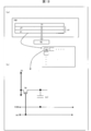
実施形態4の液晶表示装置100は、図13(a)に示すように、アクティブマトリクス基板27および対向基板(カラーフィルタ基板)37を含む液晶パネル67と、アクティブマトリクス基板27にLED光やレーザ光を照射するバックライトBLとを備える。液晶パネル67の画素PIXでは、図13(b)に示すように、液晶容量LCの画素電極がトランジスタTrを介してデータ信号線DSおよび走査信号線SCに接続され、液晶容量LCの対向電極が共通電極ラインCOMに接続されている。
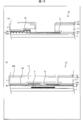
液晶パネル67には、図14に示すように、図4および図5で示した実施形態1のサイズアクティブマトリクス基板17から、遮光膜2、第1無機絶縁膜3a、下層透光膜4、第2無機絶縁膜3bおよび第3パッシベーション膜10cを省いたアクティブマトリクス基板27を用いることができる。また、図15に示すように、図4および図7で示した実施形態2のアクティブマトリクス基板17から、遮光膜2、第1無機絶縁膜3a、下層透光膜4、および第2無機絶縁膜3bおよび第3パッシベーション膜10cを省いたアクティブマトリクス基板27を用いることもできる。
〔実施形態1~4について〕
実施形態1~4のアクティブマトリクス基板では、第1金属膜9および第2金属膜12を電気的に接続しているが、これら金属膜の形成レイヤーは前記各実施形態の構成に限定されない。本発明の一態様に係るアクティブマトリクス基板は、異なる層に形成された2つの金属膜を電気的に接続する構成をもつアクティブマトリクス基板(特に、これら金属膜の接触によって電蝕のおそれがある場合)を含む表示装置全般に適用することができる。有機EL(organic electroluminescence)ディスプレイや無機EL(inorganic electro luminescence)ディスプレイについても好適である。
実施形態1~4のアクティブマトリクス基板では、第1金属膜9および第2金属膜12を電気的に接続しているが、これら金属膜の形成レイヤーは前記各実施形態の構成に限定されない。本発明の一態様に係るアクティブマトリクス基板は、異なる層に形成された2つの金属膜を電気的に接続する構成をもつアクティブマトリクス基板(特に、これら金属膜の接触によって電蝕のおそれがある場合)を含む表示装置全般に適用することができる。有機EL(organic electroluminescence)ディスプレイや無機EL(inorganic electro luminescence)ディスプレイについても好適である。
〔まとめ〕
本発明の態様1に係るアクティブマトリクス基板は、基板と、第1金属膜と、前記第1金属膜よりも上層に形成された層間絶縁膜と、層間絶縁膜よりも上層に形成された第2金属膜とを備え、前記層間絶縁膜に形成されたコンタクトホールを介して第1および第2金属膜が電気的に接続されているアクティブマトリクス基板であって、前記基板と前記第1金属膜との間の層に、導体化された酸化物半導体膜が設けられ、前記コンタクトホールの内部で前記導体化された酸化物半導体膜と前記第2金属膜とが接触し、前記コンタクトホールの外部で前記導体化された酸化物半導体膜と前記第1金属膜とが接触していることを特徴とする。
本発明の態様1に係るアクティブマトリクス基板は、基板と、第1金属膜と、前記第1金属膜よりも上層に形成された層間絶縁膜と、層間絶縁膜よりも上層に形成された第2金属膜とを備え、前記層間絶縁膜に形成されたコンタクトホールを介して第1および第2金属膜が電気的に接続されているアクティブマトリクス基板であって、前記基板と前記第1金属膜との間の層に、導体化された酸化物半導体膜が設けられ、前記コンタクトホールの内部で前記導体化された酸化物半導体膜と前記第2金属膜とが接触し、前記コンタクトホールの外部で前記導体化された酸化物半導体膜と前記第1金属膜とが接触していることを特徴とする。
本発明の態様2に係るアクティブマトリクス基板は、前記態様2において、前記第1金属膜は、前記コンタクトホールと重畳しない構成である。
本発明の態様3に係るアクティブマトリクス基板は、前記態様1または2において、前記導体化された酸化物半導体膜は、前記コンタクトホールの内側領域の全体と重なる構成である。
本発明の態様4に係るアクティブマトリクス基板は、前記態様2において、前記第1金属膜の端部は、前記コンタクトホールの側壁と向かう合う端面を有し、前記端面から前記コンタクトホールの側壁までの距離が、前記層間絶縁膜の厚みよりも小さい構成である。
本発明の態様5に係るアクティブマトリクス基板は、前記態様2において、前記第1金属膜の端部は、前記コンタクトホールから離れた位置にあり、前記第1金属配線の端部と、前記コンタクトホールの内部の第2金属膜との間に空洞が形成されている構成である。
本発明の態様6に係るアクティブマトリクス基板は、前記態様1~5のいずれか1つにおいて、前記第2金属膜は透光金属膜である構成である。
本発明の態様7に係るアクティブマトリクス基板は、前記態様1~6のいずれか1つにおいて、前記導体化された酸化物半導体膜は、トランジスタのチャネルとして機能する酸化物半導体膜と同一層に形成された導電膜である構成である。
本発明の態様8に係るアクティブマトリクス基板は、前記態様1~7のいずれか1つにおいて、前記第1金属膜にアルミニウムが含まれている構成である。
本発明の態様9に係る光シャッタ基板は、前記態様1~7のいずれか1つのアクティブマトリクス基板と、前記アクティブマトリクス基板上に形成された光シャッタ機構とを備える。
本発明の態様10に係る表示装置は、前記態様1~7のいずれか1つのアクティブマトリクス基板を備える。
本発明の態様11に係るアクティブマトリクス基板の製造方法は、酸化物半導体膜を形成する第1工程と、前記酸化物半導体膜の上層に第1金属膜を形成する第2工程と、前記第1金属膜の上層に層間絶縁膜を形成する第3工程と、前記層間絶縁膜にコンタクトホールを形成して前記酸化物半導体膜を露出させる第4工程と、前記酸化物半導体膜にプラズマ処理を施すことで、前記酸化物半導体膜を導電膜とする第5工程と、前記コンタクトホールの内部の前記導電膜を覆うように第2金属膜を形成する第6工程とを含むことを特徴とする。
本発明の態様12に係るアクティブマトリクス基板の製造方法は、前記態様11において、前記第2工程では、前記コンタクトホールの形成位置と重ならず、かつ前記酸化物半導体膜と接触するように前記第1金属膜を形成する手法である。
本発明の態様13に係るアクティブマトリクス基板の製造方法は、前記態様11において、前記第2工程では、前記コンタクトホールの形成位置と重なり、かつ前記酸化物半導体膜と接触するように第1金属膜を形成し、前記第4および第5工程の間に、前記第1金属膜を、前記酸化物半導体膜とは接触するが、前記コンタクトホールには重ならないようにエッチングする手法である。
本発明は上述した実施形態に限定されるものではなく、請求項に示した範囲で種々の変更が可能であり、異なる実施形態にそれぞれ開示された技術的手段を適宜組み合わせて得られる実施形態についても本発明の技術的範囲に含まれる。さらに、各実施形態にそれぞれ開示された技術的手段を組み合わせることにより、新しい技術的特徴を形成することができる。
1 ガラス基板
2 遮光膜
4 下層透光膜
5 下層金属膜
6 ゲート絶縁膜
7 酸化物半導体膜
7s 酸化物半導体膜
7c 導電膜(導体化された酸化物半導体膜)
9 第1金属膜
10a~10c 第1~第3パッシベーション膜
11 上層透光膜
12 第2金属膜
13 上層金属膜
17 アクティブマトリクス基板
20 光シャッタ基板
21 光シャッタ機構
22x・22y 駆動ビーム
23x・23y シャッタビーム
27 アクティブマトリクス基板
28 シャッタ体
30 対向基板
LW 光透過経路
F 層間絶縁膜
2 遮光膜
4 下層透光膜
5 下層金属膜
6 ゲート絶縁膜
7 酸化物半導体膜
7s 酸化物半導体膜
7c 導電膜(導体化された酸化物半導体膜)
9 第1金属膜
10a~10c 第1~第3パッシベーション膜
11 上層透光膜
12 第2金属膜
13 上層金属膜
17 アクティブマトリクス基板
20 光シャッタ基板
21 光シャッタ機構
22x・22y 駆動ビーム
23x・23y シャッタビーム
27 アクティブマトリクス基板
28 シャッタ体
30 対向基板
LW 光透過経路
F 層間絶縁膜
Claims (13)
- 基板と、第1金属膜と、前記第1金属膜よりも上層に形成された層間絶縁膜と、層間絶縁膜よりも上層に形成された第2金属膜とを備え、前記層間絶縁膜に形成されたコンタクトホールを介して第1および第2金属膜が電気的に接続されているアクティブマトリクス基板であって、
前記基板と前記第1金属膜との間の層に、導体化された酸化物半導体膜が設けられ、
前記コンタクトホールの内部で前記導体化された酸化物半導体膜と前記第2金属膜とが接触し、
前記コンタクトホールの外部で前記導体化された酸化物半導体膜と前記第1金属膜とが接触していることを特徴とするアクティブマトリクス基板。 - 前記第1金属膜は、前記コンタクトホールと重畳しないことを特徴とする請求項1記載のアクティブマトリクス基板。
- 前記導体化された酸化物半導体膜は、前記コンタクトホールの内側領域の全体と重なることを特徴とする請求項1または2記載のアクティブマトリクス基板。
- 前記第1金属膜の端部は、前記コンタクトホールの側壁と向かう合う端面を有し、
前記端面から前記コンタクトホールの側壁までの距離が、前記層間絶縁膜の厚みよりも小さいことを特徴とする請求項2記載のアクティブマトリクス基板。 - 前記第1金属膜の端部は、前記コンタクトホールから離れた位置にあり、前記第1金属膜の端部と、前記コンタクトホールの内部の第2金属膜との間に空洞が形成されていることを特徴とする請求項2記載のアクティブマトリクス基板。
- 前記第2金属膜は透光金属膜であることを特徴とする請求項1~5のいずれか1項に記載のアクティブマトリクス基板。
- 前記導体化された酸化物半導体膜は、トランジスタのチャネルとして機能する酸化物半導体膜と同一層に形成された導電膜であることを特徴とする請求項1~6のいずれか1項に記載のアクティブマトリクス基板。
- 前記第1金属膜にアルミニウムが含まれていることを特徴とする請求項1~7のいずれか1項に記載のアクティブマトリクス基板。
- 請求項1~8のいずれか1項に記載のアクティブマトリクス基板と、前記アクティブマトリクス基板上に形成された光シャッタ機構とを備えることを特徴とする光シャッタ基板。
- 請求項1~8のいずれか1項に記載のアクティブマトリクス基板を備えることを特徴とする表示装置。
- 酸化物半導体膜を形成する第1工程と、
前記酸化物半導体膜の上層に第1金属膜を形成する第2工程と、
前記第1金属膜の上層に層間絶縁膜を形成する第3工程と、
前記層間絶縁膜にコンタクトホールを形成して前記酸化物半導体膜を露出させる第4工程と、
前記酸化物半導体膜にプラズマ処理を施すことで、前記酸化物半導体膜を導電膜とする第5工程と、
前記コンタクトホールの内部の前記導電膜を覆うように第2金属膜を形成する第6工程とを含むことを特徴とするアクティブマトリクス基板の製造方法。 - 前記第2工程では、前記コンタクトホールの形成位置と重ならず、かつ前記酸化物半導体膜と接触するように前記第1金属膜を形成することを特徴とする請求項11記載のアクティブマトリクス基板の製造方法。
- 前記第2工程では、前記コンタクトホールの形成位置と重なり、かつ前記酸化物半導体膜と接触するように第1金属膜を形成し、前記第4および第5工程の間に、前記第1金属膜を、前記酸化物半導体膜とは接触するが、前記コンタクトホールには重ならないようにエッチングすることを特徴とする請求項11記載のアクティブマトリクス基板の製造方法。
Priority Applications (1)
| Application Number | Priority Date | Filing Date | Title |
|---|---|---|---|
| US16/305,417 US10991729B2 (en) | 2016-06-23 | 2017-06-16 | Active matrix substrate, optical shutter substrate, display device, and method for manufacturing active matrix substrate |
Applications Claiming Priority (2)
| Application Number | Priority Date | Filing Date | Title |
|---|---|---|---|
| JP2016-124791 | 2016-06-23 | ||
| JP2016124791 | 2016-06-23 |
Publications (1)
| Publication Number | Publication Date |
|---|---|
| WO2017221815A1 true WO2017221815A1 (ja) | 2017-12-28 |
Family
ID=60784732
Family Applications (1)
| Application Number | Title | Priority Date | Filing Date |
|---|---|---|---|
| PCT/JP2017/022245 Ceased WO2017221815A1 (ja) | 2016-06-23 | 2017-06-16 | アクティブマトリクス基板、光シャッタ基板、表示装置、アクティブマトリクス基板の製造方法 |
Country Status (2)
| Country | Link |
|---|---|
| US (1) | US10991729B2 (ja) |
| WO (1) | WO2017221815A1 (ja) |
Citations (8)
| Publication number | Priority date | Publication date | Assignee | Title |
|---|---|---|---|---|
| JP2008040343A (ja) * | 2006-08-09 | 2008-02-21 | Nec Corp | 薄膜トランジスタアレイ、その製造方法及び液晶表示装置 |
| WO2012020525A1 (ja) * | 2010-08-07 | 2012-02-16 | シャープ株式会社 | 薄膜トランジスタ基板及びそれを備えた液晶表示装置 |
| WO2013115043A1 (ja) * | 2012-01-31 | 2013-08-08 | シャープ株式会社 | 表示装置 |
| JP2014081416A (ja) * | 2012-10-15 | 2014-05-08 | Japan Display Inc | アパーチャープレート及びこれを備える表示装置 |
| JP2015108731A (ja) * | 2013-12-05 | 2015-06-11 | ソニー株式会社 | 半導体装置およびその製造方法、並びに表示装置および電子機器 |
| WO2015087586A1 (ja) * | 2013-12-10 | 2015-06-18 | シャープ株式会社 | 半導体装置およびその製造方法 |
| JP2016057547A (ja) * | 2014-09-11 | 2016-04-21 | シャープ株式会社 | Memsディスプレイおよびその製造方法 |
| JP2016080744A (ja) * | 2014-10-10 | 2016-05-16 | 株式会社Joled | 表示装置および電子機器 |
Family Cites Families (3)
| Publication number | Priority date | Publication date | Assignee | Title |
|---|---|---|---|---|
| DE602006003737D1 (de) | 2005-02-23 | 2009-01-02 | Pixtronix Inc | Licht-modulator und verfahren zu seiner herstellung |
| JP2010091895A (ja) * | 2008-10-10 | 2010-04-22 | Toppoly Optoelectronics Corp | アクティブマトリクス型ディスプレイ装置 |
| US20170287943A1 (en) * | 2016-03-31 | 2017-10-05 | Qualcomm Incorporated | High aperture ratio display by introducing transparent storage capacitor and via hole |
-
2017
- 2017-06-16 US US16/305,417 patent/US10991729B2/en active Active
- 2017-06-16 WO PCT/JP2017/022245 patent/WO2017221815A1/ja not_active Ceased
Patent Citations (8)
| Publication number | Priority date | Publication date | Assignee | Title |
|---|---|---|---|---|
| JP2008040343A (ja) * | 2006-08-09 | 2008-02-21 | Nec Corp | 薄膜トランジスタアレイ、その製造方法及び液晶表示装置 |
| WO2012020525A1 (ja) * | 2010-08-07 | 2012-02-16 | シャープ株式会社 | 薄膜トランジスタ基板及びそれを備えた液晶表示装置 |
| WO2013115043A1 (ja) * | 2012-01-31 | 2013-08-08 | シャープ株式会社 | 表示装置 |
| JP2014081416A (ja) * | 2012-10-15 | 2014-05-08 | Japan Display Inc | アパーチャープレート及びこれを備える表示装置 |
| JP2015108731A (ja) * | 2013-12-05 | 2015-06-11 | ソニー株式会社 | 半導体装置およびその製造方法、並びに表示装置および電子機器 |
| WO2015087586A1 (ja) * | 2013-12-10 | 2015-06-18 | シャープ株式会社 | 半導体装置およびその製造方法 |
| JP2016057547A (ja) * | 2014-09-11 | 2016-04-21 | シャープ株式会社 | Memsディスプレイおよびその製造方法 |
| JP2016080744A (ja) * | 2014-10-10 | 2016-05-16 | 株式会社Joled | 表示装置および電子機器 |
Also Published As
| Publication number | Publication date |
|---|---|
| US20200328235A1 (en) | 2020-10-15 |
| US10991729B2 (en) | 2021-04-27 |
Similar Documents
| Publication | Publication Date | Title |
|---|---|---|
| US9508747B2 (en) | Thin film transistor array substrate | |
| US8748897B2 (en) | Array substrate for organic electroluminescent display device | |
| US8883579B2 (en) | Array substrate for organic electroluminescent display device and method of fabricating the same | |
| US9548324B2 (en) | Array substrate and method for fabricating the same | |
| KR102089244B1 (ko) | 더블 게이트형 박막 트랜지스터 및 이를 포함하는 유기 발광 다이오드 표시장치 | |
| KR102081107B1 (ko) | 박막트랜지스터 어레이 기판 및 그의 제조방법 | |
| WO2018180617A1 (ja) | アクティブマトリクス基板、液晶表示装置および有機el表示装置 | |
| WO2017159413A1 (ja) | 半導体装置および半導体装置の製造方法 | |
| JP2016057547A (ja) | Memsディスプレイおよびその製造方法 | |
| US11024656B2 (en) | Active matrix substrate, optical shutter substrate, display device, and method for manufacturing active matrix substrate | |
| CN112563305A (zh) | 显示设备和修复显示设备的方法 | |
| US10670933B2 (en) | Active matrix substrate, method for producing same, and display device | |
| US10651209B2 (en) | Semiconductor device and method for manufacturing same | |
| WO2017146058A1 (ja) | 半導体装置および半導体装置の製造方法 | |
| US8889444B2 (en) | Method of manufacturing transistor, transistor, array substrate and display device | |
| TWI639851B (zh) | 顯示裝置及其製造方法 | |
| WO2017007004A1 (ja) | アクティブマトリクス基板、表示装置、及び表示装置の製造方法 | |
| CN108780221B (zh) | 显示面板、显示装置和显示面板的制造方法 | |
| CN110476200A (zh) | Tft基板、tft基板的制造方法、显示装置 | |
| WO2017007002A1 (ja) | アクティブマトリクス基板、表示装置及び製造方法 | |
| WO2017221815A1 (ja) | アクティブマトリクス基板、光シャッタ基板、表示装置、アクティブマトリクス基板の製造方法 | |
| CN107851406A (zh) | 有源矩阵基板、显示装置以及制造方法 | |
| JP2017181953A (ja) | 光シャッタ基板、プリンタヘッド | |
| WO2019187069A1 (ja) | トランジスタおよび表示装置 | |
| JP2017191297A (ja) | 光シャッタ基板、プリンタヘッド |
Legal Events
| Date | Code | Title | Description |
|---|---|---|---|
| 121 | Ep: the epo has been informed by wipo that ep was designated in this application |
Ref document number: 17815283 Country of ref document: EP Kind code of ref document: A1 |
|
| NENP | Non-entry into the national phase |
Ref country code: DE |
|
| 122 | Ep: pct application non-entry in european phase |
Ref document number: 17815283 Country of ref document: EP Kind code of ref document: A1 |
|
| NENP | Non-entry into the national phase |
Ref country code: JP |