WO2017221821A1 - Dispositif cible et appareil de pulvérisation - Google Patents
Dispositif cible et appareil de pulvérisation Download PDFInfo
- Publication number
- WO2017221821A1 WO2017221821A1 PCT/JP2017/022263 JP2017022263W WO2017221821A1 WO 2017221821 A1 WO2017221821 A1 WO 2017221821A1 JP 2017022263 W JP2017022263 W JP 2017022263W WO 2017221821 A1 WO2017221821 A1 WO 2017221821A1
- Authority
- WO
- WIPO (PCT)
- Prior art keywords
- magnet
- sputtering
- target
- plate
- disposed
- Prior art date
- Legal status (The legal status is an assumption and is not a legal conclusion. Google has not performed a legal analysis and makes no representation as to the accuracy of the status listed.)
- Ceased
Links
Images


Classifications
-
- C—CHEMISTRY; METALLURGY
- C23—COATING METALLIC MATERIAL; COATING MATERIAL WITH METALLIC MATERIAL; CHEMICAL SURFACE TREATMENT; DIFFUSION TREATMENT OF METALLIC MATERIAL; COATING BY VACUUM EVAPORATION, BY SPUTTERING, BY ION IMPLANTATION OR BY CHEMICAL VAPOUR DEPOSITION, IN GENERAL; INHIBITING CORROSION OF METALLIC MATERIAL OR INCRUSTATION IN GENERAL
- C23C—COATING METALLIC MATERIAL; COATING MATERIAL WITH METALLIC MATERIAL; SURFACE TREATMENT OF METALLIC MATERIAL BY DIFFUSION INTO THE SURFACE, BY CHEMICAL CONVERSION OR SUBSTITUTION; COATING BY VACUUM EVAPORATION, BY SPUTTERING, BY ION IMPLANTATION OR BY CHEMICAL VAPOUR DEPOSITION, IN GENERAL
- C23C14/00—Coating by vacuum evaporation, by sputtering or by ion implantation of the coating forming material
- C23C14/22—Coating by vacuum evaporation, by sputtering or by ion implantation of the coating forming material characterised by the process of coating
- C23C14/34—Sputtering
- C23C14/3407—Cathode assembly for sputtering apparatus, e.g. Target
-
- C—CHEMISTRY; METALLURGY
- C23—COATING METALLIC MATERIAL; COATING MATERIAL WITH METALLIC MATERIAL; CHEMICAL SURFACE TREATMENT; DIFFUSION TREATMENT OF METALLIC MATERIAL; COATING BY VACUUM EVAPORATION, BY SPUTTERING, BY ION IMPLANTATION OR BY CHEMICAL VAPOUR DEPOSITION, IN GENERAL; INHIBITING CORROSION OF METALLIC MATERIAL OR INCRUSTATION IN GENERAL
- C23C—COATING METALLIC MATERIAL; COATING MATERIAL WITH METALLIC MATERIAL; SURFACE TREATMENT OF METALLIC MATERIAL BY DIFFUSION INTO THE SURFACE, BY CHEMICAL CONVERSION OR SUBSTITUTION; COATING BY VACUUM EVAPORATION, BY SPUTTERING, BY ION IMPLANTATION OR BY CHEMICAL VAPOUR DEPOSITION, IN GENERAL
- C23C14/00—Coating by vacuum evaporation, by sputtering or by ion implantation of the coating forming material
- C23C14/22—Coating by vacuum evaporation, by sputtering or by ion implantation of the coating forming material characterised by the process of coating
- C23C14/34—Sputtering
- C23C14/35—Sputtering by application of a magnetic field, e.g. magnetron sputtering
-
- H—ELECTRICITY
- H01—ELECTRIC ELEMENTS
- H01J—ELECTRIC DISCHARGE TUBES OR DISCHARGE LAMPS
- H01J37/00—Discharge tubes with provision for introducing objects or material to be exposed to the discharge, e.g. for the purpose of examination or processing thereof
- H01J37/32—Gas-filled discharge tubes
- H01J37/34—Gas-filled discharge tubes operating with cathodic sputtering
- H01J37/3411—Constructional aspects of the reactor
- H01J37/3435—Target holders (includes backing plates and endblocks)
-
- H—ELECTRICITY
- H01—ELECTRIC ELEMENTS
- H01J—ELECTRIC DISCHARGE TUBES OR DISCHARGE LAMPS
- H01J37/00—Discharge tubes with provision for introducing objects or material to be exposed to the discharge, e.g. for the purpose of examination or processing thereof
- H01J37/32—Gas-filled discharge tubes
- H01J37/34—Gas-filled discharge tubes operating with cathodic sputtering
- H01J37/3411—Constructional aspects of the reactor
- H01J37/345—Magnet arrangements in particular for cathodic sputtering apparatus
Definitions
- the present invention relates to a technical field of a target device and a sputtering device using the target device, and more particularly to a target device and a sputtering device capable of uniformly sputtering a sputtering target.
- the magnetron sputtering apparatus is an apparatus that forms magnetic lines of force on the surface of a sputtering target provided in the target apparatus, spirals electrons along the lines of magnetic force, and forms a high-density plasma to sputter the sputtering target.
- a portion of the surface of the sputtering target where a magnetic field line parallel to the surface of the sputtering target is located is sputtered in a large amount.
- Patent Document 1 by arranging a plate-like magnetic member in the backing plate, a region where the vertical component of the magnetic field on the surface of the sputtering target becomes flat at or near zero is formed. (Id. Paragraph 0011).
- the target surface is dug and the thickness is reduced as the target is sputtered.
- it is necessary to break the vacuum atmosphere of the sputtering apparatus and return it to the atmosphere. For this reason, reducing the replacement frequency of the target is an important factor for improving the production efficiency of the sputtering apparatus.
- the sputtering target cannot be uniformly sputtered as the target is dug by sputtering, and the use efficiency of the target deteriorates. For this reason, even if an attempt is made to reduce the replacement frequency of the target by increasing the thickness of the target, the use efficiency of the thick target deteriorates, and as a result, there is a problem that the effect of reducing the frequency of replacing the target cannot be obtained. .
- the present invention was created to solve the above-described disadvantages of the prior art, and an object thereof is to provide a target device with high use efficiency.
- the present invention provides a backing plate, a sputtering target that is disposed on one side of the backing plate and has an exposed sputtering surface, and a side of the backing plate on which the sputtering target is disposed.
- a target device having a magnet device disposed on the opposite side, the magnet device having an upper end positioned in a magnet plane parallel to the sputtering surface of the sputtering target before being sputtered.
- a shaped outer magnet and an upper end located on the magnet plane, inside the outer magnet, arranged in a non-contact manner with the outer magnet, and a permeability larger than the permeability of the backing plate.
- the rear surface of the magnetic plate is aligned with the magnet plane or is positioned farther from the sputtering target than the magnet plane, and magnetic lines of force are formed on the sputtering surface.
- the present invention is the target device in which the high magnetic permeability plate is not in contact with the outer magnet and the inner magnet.
- the present invention is the target device in which the high permeability plate is made of a metal material having a permeability of 0.9 ⁇ 10 ⁇ 3 H / m or more.
- the present invention is a sputtering apparatus having a vacuum chamber and a target device disposed inside the vacuum chamber, wherein the target device is disposed on one side of the backing plate and the backing plate and is sputtered.
- a sputtering target having an exposed sputtering surface; and a magnet device disposed on a side of the backing plate opposite to the side on which the sputtering target is disposed, the magnet device having an upper end before sputtering.
- the outer surface of the sputtering target which is parallel to the sputtering surface of the sputtering target, has a ring-shaped outer magnet, the upper end is positioned on the magnet surface, and the outer magnet is not inside the outer magnet.
- An inner magnet arranged in contact;
- a ring-shaped high permeability plate having a permeability greater than the permeability of the backing plate, and the high permeability plate is disposed at a position surrounding the inner magnet and surrounded by the outer magnet.
- the outer side surface and the inner side surface of the high permeability plate intersect the magnet plane, or the upper end of the outer side surface and the upper end of the inner side surface or the lower end of the outer side surface and the lower end of the inner side surface are the magnets.
- the sputtering apparatus is arranged so as to coincide with a plane, and magnetic lines of force are formed on the sputtering surface.
- the present invention is the sputtering apparatus in which the high magnetic permeability plate is not in contact with the outer magnet and the inner magnet.
- the present invention is the sputtering apparatus in which the high magnetic permeability plate is made of a metal material having a magnetic permeability of 0.9 ⁇ 10 ⁇ 3 H / m or more.
- a thick sputtering target can be sputtered uniformly, so the target usage efficiency is high.
- the sputtering target can be used for a long time with high efficiency.
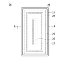
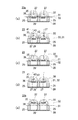
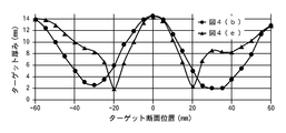
- Target apparatus and sputtering apparatus of the present invention Target device of the present invention Sectional view taken along line AA (a) to (e): drawings for explaining the positional relationship between the high permeability plate, the outer magnet, and the inner magnet Drawing for explaining a magnet device having no high permeability plate Graphs showing the magnetic field strength and width in FIGS. Graph showing the relationship between target position and thickness
- a sputtering apparatus 11 of FIG. 1 is an example of the present invention, and has a vacuum chamber 12.
- a target device 14 of the present invention is disposed inside the vacuum chamber 12.
- a plan view of the target device 14 is shown in FIG. 2, and a cross-sectional view taken along line AA is shown in FIG.
- the target device 14 has a plate-like backing plate 21, and a sputtering target 22 is disposed on one side of the backing plate 21.
- a substrate holder 17 is disposed at a position opposite to the target device 14 inside the vacuum chamber 12.
- a sputtering surface 24 that is one surface of the sputtering target 22 is exposed inside the vacuum chamber 12, and when the substrate 18 is disposed on the substrate holder 17, the film-forming surface 19 of the substrate 18 is parallel to the sputtering surface 24. Face to face.
- a vacuum exhaust device 13 and a gas supply device 16 are connected to the vacuum chamber 12. After the vacuum exhaust device 13 evacuates the inside of the vacuum chamber 12 and a vacuum atmosphere is formed inside the vacuum chamber 12. Then, sputtering gas is supplied from the gas supply device 16 to the inside of the vacuum chamber 12, and a sputtering gas atmosphere that is a vacuum state containing the sputtering gas is formed inside the vacuum chamber 12.
- a magnet device 23 is disposed near the surface of the backing plate 21 opposite to the surface on which the sputtering target 22 is disposed.
- the magnet device 23 is located on the back surface side opposite to the sputtering surface 24 of the sputtering target 22.
- the magnet device 23 is disposed on one side where a magnetically permeable material having a magnetic permeability is formed into a flat plate shape, an inner magnet 26 disposed on one side of the yoke 28, and an inner magnet 26.
- the inner magnet 26 has the first magnetic pole disposed at the end directed toward the yoke 28, and the yoke A second magnetic pole is arranged at the end facing away from 28, and the outer magnet 25 is opposite to the inner magnet 26, with the second magnetic pole at the end facing toward the yoke 28. Is disposed, and the first magnetic pole is disposed at the end facing the side opposite to the yoke 28.
- the magnetic poles there are cases where the first magnetic pole is an N pole and the second magnetic pole is an S pole, and where the first magnetic pole is an S pole and the second magnetic pole is an N pole.
- the sputtering target 22 is located via the backing plate 21 near the ends of the inner magnet 26 and the outer magnet 25 that face the opposite side of the yoke 28.
- the backing plate 21 is made of copper whose permeability is close to a vacuum value, and here, the sputtering target 22 is also made of a material close to a vacuum value.
- the magnetic field lines emitted from the N pole of the magnet device 23 penetrate the backing plate 21 and the sputtering target 22, leak onto the sputtering surface 24, bend on the sputtering surface 24, and cause the sputtering target 22 and the backing plate 21 to It penetrates and enters the south pole of the magnet device 23.
- the backing plate 21 is connected to the sputtering power source 34.
- a voltage is applied to the backing plate 21 by the sputtering power source 34 in a state where the sputtering atmosphere is formed, electrons are emitted from the surface of the cathode electrode (here, the target 22).
- the electrons emitted from the cathode electrode spirally move along the lines of magnetic force on the sputtering surface 24, generate plasma in the vicinity of the sputtering surface 24 by interaction with the sputtering gas, and the sputtering surface 24 is sputtered.
- the part where the magnetic component in the vertical direction is zero that is, the part of the magnetic force lines leaked onto the sputter surface 24 that extends in a direction parallel to the sputter surface 24.
- the plasma immediately below has a high density, and a portion of the sputtering surface 24 that comes into contact with the high density plasma is sputtered in a large amount.
- a resin 29 is disposed between the outer magnet 25 and the inner magnet 26, and the outer magnet 25 and the inner magnet 26 are separated from each other by the resin 29. It is fixed in the state.
- a ring-shaped high permeability plate 27 surrounding the inner magnet 26 is disposed, and there are many magnetic lines extending in parallel with the sputtering surface 24 as described later.
- FIG. 5 shows a magnet device 33 d in which the high permeability plate 27 is not disposed, and the magnetic lines of force 30 formed by the magnet device 33 d are curved so as to have a maximum value at a substantially intermediate position between the outer magnet 25 and the inner magnet 26. In the magnetic field lines 30, there are few portions extending in parallel with the sputtering surface 24.
- the magnet devices 23, 33a, and 33b in FIGS. 4 (a) to 4 (e) have a high permeability plate 27, and the resin 29 is not shown.
- a gap is provided between the outer periphery of the high permeability plate 27 and the inner periphery of the outer magnet 25, and between the inner periphery of the high permeability plate 27 and the outer periphery of the inner magnet 26, and the high permeability.
- the plate 27 is made non-contact with the outer magnet 25 and is also made non-contact with the inner magnet 26 so that excessive magnetic lines 30 do not pass through the high permeability plate 27 and the shape of the magnetic lines 30 is biased. There has been no such thing.
- the upper end of the outer magnet 25 and the upper end of the inner magnet 26 are located on the same magnet plane 31 in parallel with the sputtering surface 24 of the sputtering target 22 that has not yet been sputtered.
- the high magnetic permeability plate 27 is made of a material having a magnetic permeability larger than that of the backing plate 21 and has a magnetic permeability larger than that of vacuum or air, so that the gap between the outer magnet 25 and the inner magnet 26 is high.
- some of the magnetic field lines 30 enter the inside of the high magnetic permeability plate 27 from either the vicinity of the outer periphery or the inner periphery of the high permeability plate 27, and the inside of the high permeability plate 27. Through the other side.
- the high permeability plate 27 includes a surface 33 of the high permeability plate 27 that coincides with the magnet plane 31 and is opposite to the surface 33 of the high permeability plate 27. 4 is disposed farther from the sputtering target 22 than the magnet plane 31, and in the magnet device 23 of FIG. 4C, the surface 33 of the high permeability plate 27 is sputtered from the magnet plane 31.
- the back surface 32 located near the target 22 and opposite to the surface 33 of the high permeability plate 27 is disposed so as to be located farther from the sputtering target 22 than the magnet plane 31.
- the high magnetic permeability plate 27 is disposed so that the back surface 32 of the high magnetic permeability plate 27 coincides with the magnet plane 31.
- the magnetic line 30 formed between the upper end of the outer magnet 25 and the upper end of the inner magnet 25 is referred to as an upper magnetic line 35.
- the magnetic field lines 30 formed between the vicinity of the outer edge of the inner magnet 26 and the vicinity of the inner periphery of the outer magnet 25 are referred to as lower magnetic field lines 36, sputtering is performed at a predetermined distance from the upper end of the outer magnet 25 and the upper end of the inner magnet 26.
- the upper magnetic field line 35 leaks in a semi-annular manner and winds electrons, while the lower magnetic field line 36 does not leak on the sputtering surface 24, but the high magnetic permeability plate 27 is not provided.
- the lower magnetic force line 36 pushes up the central portion of the upper magnetic force line 35, so that the upper magnetic force line 35 is curved on the sputter surface 24 and flat with the sputter surface 24.
- the portion of the magnetic field lines 30 extending to decrease.
- the magnet devices 23, 33a and 33b shown in FIGS. 4 (a) to 4 (e) having the high permeability plate 27 the magnet devices shown in FIGS. 4 (b), (c) and (d) used in the present invention.
- a part of the lower magnetic force line 36 enters the high permeability plate 27 from one of the vicinity of the outer periphery or the inner periphery of the high permeability plate 27, passes through the high permeability plate 27, It leaks out of the high permeability plate 27 from the other vicinity.
- the lower magnetic field lines 36 passing outside the high magnetic permeability plate 27 are reduced, so that the central part of the upper magnetic field line 35 is not pressed from below and extends parallel to the sputtering surface 24.
- the area increases and the area to be sputtered increases.
- the second line segment 42 of the magnet device 23 in FIG. It extends from the inner periphery of the upper end to the outer edge of the upper end of the inner magnet 26, and in FIGS. 4 (b) and 4 (d), the singular point 43 is formed near the upper magnetic field line 35 and the lower magnetic field line 36. I understand.
- the left vertical axis indicates the horizontal magnetic field strength at the singular point
- the right vertical axis indicates the width of the magnetic field lines having a magnetic field strength of ⁇ 5 G in the horizontal direction at the singular point (parallel to the magnet plane 31).
- 6 is a straight line direction in a straight plane and is a length in a straight line direction perpendicular to the straight line indicating the distance between the outer magnet 25 and the inner magnet 26).
- the magnetic device 23 in FIGS. 4B, 4 ⁇ / b> C, and 4 ⁇ / b> D has a magnetic field strength within a range of 140 G or more and 230 G or less.
- the width of the magnetic field lines having a magnetic field strength of ⁇ 5 G exceeds 10 mm in any of the magnet devices 23, 33a, 33b, and a wide sputter region can be obtained. That is, since the magnet device 23 shown in FIGS. 4B, 4C, and 4D does not greatly reduce the semicircular magnetic field lines on the sputtering surface 24, the thick sputtering target 22 can be sputtered uniformly. it can.
- the horizontal magnetic field strength at the singular point 43 was 208 G, and the width of the magnetic field lines having a magnetic field strength of ⁇ 5 G was 13 mm.
- the horizontal magnetic field strength at the singular point is 119G, and the width of the magnetic field lines having a magnetic field strength of ⁇ 5G is 15 mm.
- the magnetic field strength is 119G, which is smaller than 140G. For this reason, the discharge is not stable, the magnetic field lines are concentrated, and the discharge is concentrated on the central side where the magnetic field is relatively strong. It is considered that the amount sputtered due to this has been biased.
- the magnetic field strength is 208 G, which falls within the range of 140 G to 230 G, and the width of the magnetic field lines is as wide as 13 mm. It is considered that a wide sputter region can be obtained even after the progress.
- the thickness of the high magnetic permeability plate 27 is about several mm, and a plate made of stainless steel, iron, permalloy in a flat plate shape, or a plate made of other magnetic permeability material can be used.
- the magnetic permeability ⁇ (H / m) of copper constituting the backing plate is 1.26 ⁇ 10 ⁇ 6
- the material constituting the high magnetic permeability plate 27 of the present invention is martensitic stainless steel (annealed: 9.42).
Landscapes
- Chemical & Material Sciences (AREA)
- Engineering & Computer Science (AREA)
- Chemical Kinetics & Catalysis (AREA)
- Materials Engineering (AREA)
- Mechanical Engineering (AREA)
- Metallurgy (AREA)
- Organic Chemistry (AREA)
- Physics & Mathematics (AREA)
- Plasma & Fusion (AREA)
- Analytical Chemistry (AREA)
- Physical Vapour Deposition (AREA)
Abstract
Priority Applications (3)
| Application Number | Priority Date | Filing Date | Title |
|---|---|---|---|
| JP2018524025A JP6612448B2 (ja) | 2016-06-21 | 2017-06-16 | ターゲット装置、スパッタリング装置 |
| KR1020187035177A KR20190003747A (ko) | 2016-06-21 | 2017-06-16 | 타겟 장치, 스퍼터링 장치 |
| CN201780038787.2A CN109312450B (zh) | 2016-06-21 | 2017-06-16 | 靶材装置、溅射装置 |
Applications Claiming Priority (2)
| Application Number | Priority Date | Filing Date | Title |
|---|---|---|---|
| JP2016-123050 | 2016-06-21 | ||
| JP2016123050 | 2016-06-21 |
Publications (1)
| Publication Number | Publication Date |
|---|---|
| WO2017221821A1 true WO2017221821A1 (fr) | 2017-12-28 |
Family
ID=60784109
Family Applications (1)
| Application Number | Title | Priority Date | Filing Date |
|---|---|---|---|
| PCT/JP2017/022263 Ceased WO2017221821A1 (fr) | 2016-06-21 | 2017-06-16 | Dispositif cible et appareil de pulvérisation |
Country Status (5)
| Country | Link |
|---|---|
| JP (1) | JP6612448B2 (fr) |
| KR (1) | KR20190003747A (fr) |
| CN (1) | CN109312450B (fr) |
| TW (1) | TW201812065A (fr) |
| WO (1) | WO2017221821A1 (fr) |
Families Citing this family (2)
| Publication number | Priority date | Publication date | Assignee | Title |
|---|---|---|---|---|
| JP2019183192A (ja) * | 2018-04-03 | 2019-10-24 | 株式会社アルバック | スパッタリング装置 |
| JP6982597B2 (ja) * | 2019-06-26 | 2021-12-17 | 株式会社アルバック | スパッタリング装置 |
Citations (7)
| Publication number | Priority date | Publication date | Assignee | Title |
|---|---|---|---|---|
| JPH02277772A (ja) * | 1989-01-30 | 1990-11-14 | Mitsubishi Kasei Corp | マグネトロンスパッタ装置 |
| JPH0445267A (ja) * | 1990-06-12 | 1992-02-14 | Matsushita Electric Ind Co Ltd | スパッタリング装置 |
| JPH04501585A (ja) * | 1988-11-14 | 1992-03-19 | ハウザー インダストリーズ ビーヴイ | 改良されたマグネトロンスパッタリング陰極 |
| JPH07188918A (ja) * | 1993-12-27 | 1995-07-25 | Sumitomo Metal Mining Co Ltd | マグネトロンスパッタ装置 |
| JPH11500490A (ja) * | 1993-10-22 | 1999-01-12 | マンリー,ケリー | 磁性ターゲット材料のスパッタ方法及び装置 |
| JP2005008917A (ja) * | 2003-06-17 | 2005-01-13 | Nitto Denko Corp | マグネトロンスパッタ装置用カソード |
| WO2012035603A1 (fr) * | 2010-09-13 | 2012-03-22 | 株式会社シンクロン | Dispositif de production de champ magnétique, cathode de magnétron, et dispositif de pulvérisation cathodique |
-
2017
- 2017-06-16 WO PCT/JP2017/022263 patent/WO2017221821A1/fr not_active Ceased
- 2017-06-16 CN CN201780038787.2A patent/CN109312450B/zh active Active
- 2017-06-16 KR KR1020187035177A patent/KR20190003747A/ko not_active Ceased
- 2017-06-16 JP JP2018524025A patent/JP6612448B2/ja active Active
- 2017-06-20 TW TW106120611A patent/TW201812065A/zh unknown
Patent Citations (7)
| Publication number | Priority date | Publication date | Assignee | Title |
|---|---|---|---|---|
| JPH04501585A (ja) * | 1988-11-14 | 1992-03-19 | ハウザー インダストリーズ ビーヴイ | 改良されたマグネトロンスパッタリング陰極 |
| JPH02277772A (ja) * | 1989-01-30 | 1990-11-14 | Mitsubishi Kasei Corp | マグネトロンスパッタ装置 |
| JPH0445267A (ja) * | 1990-06-12 | 1992-02-14 | Matsushita Electric Ind Co Ltd | スパッタリング装置 |
| JPH11500490A (ja) * | 1993-10-22 | 1999-01-12 | マンリー,ケリー | 磁性ターゲット材料のスパッタ方法及び装置 |
| JPH07188918A (ja) * | 1993-12-27 | 1995-07-25 | Sumitomo Metal Mining Co Ltd | マグネトロンスパッタ装置 |
| JP2005008917A (ja) * | 2003-06-17 | 2005-01-13 | Nitto Denko Corp | マグネトロンスパッタ装置用カソード |
| WO2012035603A1 (fr) * | 2010-09-13 | 2012-03-22 | 株式会社シンクロン | Dispositif de production de champ magnétique, cathode de magnétron, et dispositif de pulvérisation cathodique |
Also Published As
| Publication number | Publication date |
|---|---|
| KR20190003747A (ko) | 2019-01-09 |
| CN109312450A (zh) | 2019-02-05 |
| CN109312450B (zh) | 2021-01-12 |
| TW201812065A (zh) | 2018-04-01 |
| JP6612448B2 (ja) | 2019-11-27 |
| JPWO2017221821A1 (ja) | 2018-08-02 |
Similar Documents
| Publication | Publication Date | Title |
|---|---|---|
| US10134557B2 (en) | Linear anode layer slit ion source | |
| CN102725435B (zh) | 磁场产生装置、磁控管阴极及溅射装置 | |
| CN103168338B (zh) | 具有大靶的用于高压溅射的溅射源和溅射方法 | |
| CN103562433B (zh) | 跑道形状的磁控溅射用磁场产生装置 | |
| US8778150B2 (en) | Magnetron sputtering cathode, magnetron sputtering apparatus, and method of manufacturing magnetic device | |
| CN101519769A (zh) | 一种改善磁场分布的平面磁控溅射靶 | |
| JP6612448B2 (ja) | ターゲット装置、スパッタリング装置 | |
| JP2010248576A (ja) | マグネトロンスパッタリング装置 | |
| TW201941241A (zh) | 離子槍 | |
| JP5080294B2 (ja) | イオンガン及び成膜装置 | |
| JP2002088466A (ja) | 真空アーク蒸発装置 | |
| JPH0159351B2 (fr) | ||
| KR101629131B1 (ko) | 아크식 증발원 | |
| JP2007291477A (ja) | スパッタリング装置 | |
| JP5124317B2 (ja) | シートプラズマ成膜装置、及びシートプラズマ調整方法 | |
| JP2008025001A (ja) | マグネトロンスパッタリング装置 | |
| JP2604442B2 (ja) | マグネトロンスパッタ装置 | |
| JP4219925B2 (ja) | マグネトロンスパッタ装置 | |
| JP2005290442A (ja) | Ecrスパッタリング装置 | |
| JP2016023329A (ja) | マグネトロンスパッタリング装置、バッキングプレート、ターゲット組立体、及びマグネトロンスパッタリング方法 | |
| JP5561948B2 (ja) | イオン源 | |
| TWM588132U (zh) | 輔助陽極與濺鍍設備 | |
| JPWO2015076162A1 (ja) | プラズマ電極、プラズマ処理電極、cvd電極、プラズマcvd装置及び薄膜付基材の製造方法 | |
| JP2011044415A (ja) | 板状陰極表面処理装置 | |
| CN101570852A (zh) | 一种用于溅射镀膜的阴极 |
Legal Events
| Date | Code | Title | Description |
|---|---|---|---|
| ENP | Entry into the national phase |
Ref document number: 2018524025 Country of ref document: JP Kind code of ref document: A |
|
| 121 | Ep: the epo has been informed by wipo that ep was designated in this application |
Ref document number: 17815289 Country of ref document: EP Kind code of ref document: A1 |
|
| ENP | Entry into the national phase |
Ref document number: 20187035177 Country of ref document: KR Kind code of ref document: A |
|
| NENP | Non-entry into the national phase |
Ref country code: DE |
|
| 122 | Ep: pct application non-entry in european phase |
Ref document number: 17815289 Country of ref document: EP Kind code of ref document: A1 |