WO2017221992A1 - 電波吸収シート - Google Patents
電波吸収シート Download PDFInfo
- Publication number
- WO2017221992A1 WO2017221992A1 PCT/JP2017/022912 JP2017022912W WO2017221992A1 WO 2017221992 A1 WO2017221992 A1 WO 2017221992A1 JP 2017022912 W JP2017022912 W JP 2017022912W WO 2017221992 A1 WO2017221992 A1 WO 2017221992A1
- Authority
- WO
- WIPO (PCT)
- Prior art keywords
- radio wave
- wave absorption
- layer
- absorption layer
- sheet
- Prior art date
- Legal status (The legal status is an assumption and is not a legal conclusion. Google has not performed a legal analysis and makes no representation as to the accuracy of the status listed.)
- Ceased
Links
Images


Classifications
-
- H—ELECTRICITY
- H01—ELECTRIC ELEMENTS
- H01Q—ANTENNAS, i.e. RADIO AERIALS
- H01Q17/00—Devices for absorbing waves radiated from an antenna; Combinations of such devices with active antenna elements or systems
- H01Q17/004—Devices for absorbing waves radiated from an antenna; Combinations of such devices with active antenna elements or systems using non-directional dissipative particles, e.g. ferrite powders
-
- B—PERFORMING OPERATIONS; TRANSPORTING
- B32—LAYERED PRODUCTS
- B32B—LAYERED PRODUCTS, i.e. PRODUCTS BUILT-UP OF STRATA OF FLAT OR NON-FLAT, e.g. CELLULAR OR HONEYCOMB, FORM
- B32B15/00—Layered products comprising a layer of metal
- B32B15/04—Layered products comprising a layer of metal comprising metal as the main or only constituent of a layer, which is next to another layer of the same or of a different material
- B32B15/08—Layered products comprising a layer of metal comprising metal as the main or only constituent of a layer, which is next to another layer of the same or of a different material of synthetic resin
-
- H—ELECTRICITY
- H01—ELECTRIC ELEMENTS
- H01F—MAGNETS; INDUCTANCES; TRANSFORMERS; SELECTION OF MATERIALS FOR THEIR MAGNETIC PROPERTIES
- H01F1/00—Magnets or magnetic bodies characterised by the magnetic materials therefor; Selection of materials for their magnetic properties
- H01F1/01—Magnets or magnetic bodies characterised by the magnetic materials therefor; Selection of materials for their magnetic properties of inorganic materials
- H01F1/03—Magnets or magnetic bodies characterised by the magnetic materials therefor; Selection of materials for their magnetic properties of inorganic materials characterised by their coercivity
- H01F1/12—Magnets or magnetic bodies characterised by the magnetic materials therefor; Selection of materials for their magnetic properties of inorganic materials characterised by their coercivity of soft-magnetic materials
- H01F1/34—Magnets or magnetic bodies characterised by the magnetic materials therefor; Selection of materials for their magnetic properties of inorganic materials characterised by their coercivity of soft-magnetic materials non-metallic substances, e.g. ferrites
-
- H—ELECTRICITY
- H01—ELECTRIC ELEMENTS
- H01F—MAGNETS; INDUCTANCES; TRANSFORMERS; SELECTION OF MATERIALS FOR THEIR MAGNETIC PROPERTIES
- H01F1/00—Magnets or magnetic bodies characterised by the magnetic materials therefor; Selection of materials for their magnetic properties
- H01F1/01—Magnets or magnetic bodies characterised by the magnetic materials therefor; Selection of materials for their magnetic properties of inorganic materials
- H01F1/03—Magnets or magnetic bodies characterised by the magnetic materials therefor; Selection of materials for their magnetic properties of inorganic materials characterised by their coercivity
- H01F1/12—Magnets or magnetic bodies characterised by the magnetic materials therefor; Selection of materials for their magnetic properties of inorganic materials characterised by their coercivity of soft-magnetic materials
- H01F1/34—Magnets or magnetic bodies characterised by the magnetic materials therefor; Selection of materials for their magnetic properties of inorganic materials characterised by their coercivity of soft-magnetic materials non-metallic substances, e.g. ferrites
- H01F1/342—Oxides
-
- H—ELECTRICITY
- H05—ELECTRIC TECHNIQUES NOT OTHERWISE PROVIDED FOR
- H05K—PRINTED CIRCUITS; CASINGS OR CONSTRUCTIONAL DETAILS OF ELECTRIC APPARATUS; MANUFACTURE OF ASSEMBLAGES OF ELECTRICAL COMPONENTS
- H05K9/00—Screening of apparatus or components against electric or magnetic fields
-
- H—ELECTRICITY
- H05—ELECTRIC TECHNIQUES NOT OTHERWISE PROVIDED FOR
- H05K—PRINTED CIRCUITS; CASINGS OR CONSTRUCTIONAL DETAILS OF ELECTRIC APPARATUS; MANUFACTURE OF ASSEMBLAGES OF ELECTRICAL COMPONENTS
- H05K9/00—Screening of apparatus or components against electric or magnetic fields
- H05K9/0073—Shielding materials
- H05K9/0075—Magnetic shielding materials
-
- B—PERFORMING OPERATIONS; TRANSPORTING
- B32—LAYERED PRODUCTS
- B32B—LAYERED PRODUCTS, i.e. PRODUCTS BUILT-UP OF STRATA OF FLAT OR NON-FLAT, e.g. CELLULAR OR HONEYCOMB, FORM
- B32B2307/00—Properties of the layers or laminate
- B32B2307/40—Properties of the layers or laminate having particular optical properties
- B32B2307/416—Reflective
Definitions
- the present disclosure relates to a radio wave absorbing sheet that absorbs radio waves, and in particular, radio waves that can absorb radio waves having a frequency ranging from several tens of gigahertz (GHz) to several hundred gigahertz (GHz) to 3 terahertz (THz). It relates to an absorbent sheet.
- GHz gigahertz
- GHz gigahertz
- THz terahertz
- Radio waves called centimeter waves having a frequency band of several gigahertz (GHz) are used in mobile communications such as mobile phones, wireless LANs, automatic toll collection systems (ETC), and the like.
- Patent Document 1 As a radio wave absorbing sheet that absorbs such a centimeter wave, a laminate sheet in which a rubbery radio wave absorbing sheet and a paper-like sheet material such as cardboard are laminated has been proposed (see Patent Document 1). In addition, radio wave absorption with stable radio wave absorption characteristics regardless of the radio wave incident direction by laminating thin sheets containing anisotropic graphite and binder alternately in the H and Y directions and adjusting their thickness A sheet has been proposed (see Patent Document 2).
- radio waves in a frequency band of 20 GHz or higher can be absorbed.
- An electromagnetic wave absorbing sheet has been proposed (see Patent Document 3).
- a radio wave absorbing sheet that is indispensable for preventing leaked radio waves as one of radio wave utilization technologies is limited to a frequency corresponding to a frequency of about 20 GHz up to several tens of GHz at the present time.
- a radio wave absorbing sheet that can absorb radio waves in the entire millimeter wave band of gigahertz or higher frequency bands up to 3 terahertz has not been realized.
- the present disclosure aims to solve the above-described conventional problems and to realize a radio wave absorbing sheet that can absorb radio waves having a high frequency of a millimeter wave band or higher and that can be easily handled.
- a radio wave absorption sheet disclosed in the present application is a radio wave absorption sheet provided with a flexible radio wave absorption layer including a particulate radio wave absorption material and a resin binder, and the radio wave absorption material Is magnetic iron oxide that magnetically resonates in a frequency band greater than or equal to the millimeter wave band.
- the radio wave absorption sheet disclosed in the present application includes magnetic iron oxide that magnetically resonates in a high frequency band of millimeter waves or more as a radio wave absorption material in a radio wave absorption layer. Can be converted. Further, since the radio wave absorption layer includes a resin binder, it can be realized as a flexible radio wave absorption sheet that absorbs radio waves in a high frequency band.
- the radio wave absorption sheet disclosed in the present application is a radio wave absorption sheet including a flexible radio wave absorption layer including a particulate radio wave absorption material and a resin binder, and the radio wave absorption material has a millimeter wave band or more. It is magnetic iron oxide that magnetically resonates in the frequency band.
- the radio wave absorption sheet disclosed in the present application can absorb radio waves in a high frequency band of 30 GHz or more, which is a millimeter wave band, by magnetic resonance of the radio wave absorbing material.
- a flexible radio wave absorbing sheet can be realized by using a particulate radio wave absorbing material and a resin binder. For this reason, it is possible to provide a radio wave absorbing sheet that is easy to handle and can be used for high frequency radio waves in the future, such as millimeter wave radar and communication at high frequencies of several tens of gigahertz.
- the radio wave absorption sheet disclosed in the present application preferably further includes a dispersant for dispersing the radio wave absorption material in the radio wave absorption layer.
- the dispersant is preferably a phosphoric acid compound.
- the radio wave absorbing material is epsilon iron oxide.
- epsilon iron oxide as a radio wave absorber that absorbs radio waves having a frequency higher than 30 GHz as a radio wave absorbing material, a radio wave absorbing sheet that absorbs radio waves of high frequency can be realized.
- a part of the Fe site of the epsilon iron oxide is substituted with a trivalent metal atom.
- a radio wave absorbing sheet that absorbs radio waves in a desired frequency band can be realized by taking advantage of the characteristics of epsilon magnetic iron oxide having different magnetic resonance frequencies depending on the material replacing the Fe site.
- the volume content of the magnetic iron oxide in the radio wave absorbing layer is preferably 30% or more.
- the resin binder preferably contains at least one of a sulfonic acid group and a carboxyl group and is halogen-free.
- the radio wave absorption layer may have a thickness of 1 mm or less.
- a reflection layer made of a metal plate, a metal foil, or a metal vapor deposition film is formed in contact with one surface of the radio wave absorption layer.
- the reflective layer and the radio wave absorption layer are sequentially laminated on a resin base material, and an adhesive layer is provided on the surface of the base material opposite to the side where the radio wave absorption layer is disposed. Is preferably formed.
- FIG. 1 is a cross-sectional view illustrating a configuration of a radio wave absorbing sheet according to the present embodiment.
- FIG. 1 is a figure described in order to make it easy to understand the configuration of the radio wave absorption sheet according to the present embodiment, and the size and thickness of the members shown in the figure are represented in reality. It is not a thing.
- the radio wave absorption sheet exemplified in this embodiment includes a radio wave absorption layer 1 including a particulate radio wave absorption material 1a and a resin binder 1b.
- a reflective layer 2 made of a metal material is formed on the back side (lower side in FIG. 1) of the radio wave absorption layer 1, and a laminate of the radio wave absorption layer 1 and the reflective layer 2 is formed.
- the base film 3 is a resin base material.
- an adhesive layer 4 is formed on the side (lower side in FIG. 1) opposite to the side (upper side in FIG. 1) on which the radio wave absorbing layer 1 is disposed.
- the radio wave absorption sheet according to the present embodiment absorbs a radio wave that is an electromagnetic wave by converting it into heat energy by magnetic loss when the radio wave absorption material 1a included in the radio wave absorption layer 1 causes magnetic resonance to absorb the radio wave. Only the absorption layer 1 can absorb radio waves. For this reason, as a non-resonant type (transmission type) radio wave absorption sheet provided with only the radio wave absorption layer 1, it is possible to adopt a mode of absorbing transmitted radio waves.
- radio waves are incident from one side of the radio wave absorption layer 1, and the reflective layer 2 is a metal layer on the other side of the radio wave absorption layer 1, that is, the back side with respect to the radio wave incidence side.
- the radio wave incident on the radio wave absorption layer 1 is reliably shielded, and the radio wave absorption layer 1 absorbs the radio wave and is emitted as a reflected wave.
- the intensity of radio waves can be reduced.
- the radio wave absorption sheet of the present embodiment impedance matching is performed to adjust the thickness of the radio wave absorption layer 1 based on the frequency of the radio wave to be absorbed.
- the radio wave absorbing layer 1 is a non-resonant type that does not include a reflective layer, and has a reflective layer 2 with a thickness of 3 mm or less.
- the resonance type a thin sheet having a thickness of 1 mm or less is obtained.
- the base film 3 which is a resin base material having a predetermined thickness
- it is easy to handle as a radio wave absorption sheet. Can be improved.
- the base film 3 is not required.
- the radio wave absorbing sheet according to the present embodiment is often used by being attached to the surface of a member around a high frequency radio wave generation source, by laminating the adhesive layer 4 on the base film 3, the radio wave absorbing sheet can be further increased. The ease of handling of the absorbent sheet is improved.
- the adhesive layer 4 can be laminated on the radio wave absorption layer 1 and the reflective layer 2.
- radio wave absorbing material In the radio wave absorbing sheet according to this embodiment, magnetic iron oxide powders such as epsilon iron oxide magnetic powder, barium ferrite magnetic powder, and strontium ferrite magnetic powder can be used as the particulate radio wave absorbing material.
- epsilon iron oxide has a high precession frequency when the electrons of the iron atom spin, and has a high effect of absorbing radio waves having a high frequency of 30 to 300 gigahertz or more in the millimeter wave band. Therefore, it is particularly suitable as a radio wave absorbing material.
- Epsilon iron oxide ( ⁇ -Fe 2 O 3 ) is used between ferric oxide (Fe 2 O 3 ) and between alpha phase ( ⁇ -Fe 2 O 3 ) and gamma phase ( ⁇ -Fe 2 O 3 ). It is a magnetic material that appears in a single-phase state by a nanoparticle synthesis method that combines a reverse micelle method and a sol-gel method.
- Epsilon iron oxide is a fine particle with an average particle diameter of several nanometers to several tens of nanometers, and has the largest coercive force as a metal oxide of about 20 kOe at room temperature. Furthermore, natural magnetism due to a gyromagnetic effect based on precession Resonance occurs in a so-called millimeter-wave frequency band of several tens of gigahertz or more.
- epsilon iron oxide is a crystal in which part of the Fe site of the crystal is replaced with a trivalent metal element such as aluminum (Al), gallium (Ga), rhodium (Rh), or indium (In).
- the magnetic resonance frequency that is, the frequency of radio waves absorbed when used as a radio wave absorbing material can be varied.
- FIG. 2 shows the relationship between the coercive force Hc of epsilon iron oxide and the natural resonance frequency f when the metal element substituted for the Fe site is different. Note that the natural resonance frequency f matches the frequency of the radio wave to be absorbed.
- the natural resonance frequency of epsilon iron oxide in which a part of the Fe site is substituted differs depending on the type of the substituted metal element and the amount of substitution. Moreover, it turns out that the coercive force of the said epsilon iron oxide becomes large, so that the value of the natural resonance frequency becomes high.
- a frequency band from about 30 GHz to about 150 GHz is obtained.
- aluminum-substituted epsilon iron oxide having an absorption peak that is, ⁇ -Al x Fe 2-x O 3
- the frequency band of about 100 to 190 GHz can be adjusted by adjusting the substitution amount “x”. Has an absorption peak.
- the type of element to be replaced with the Fe site of epsilon iron oxide is determined so that the natural resonance frequency of the frequency to be absorbed by the radio wave absorbing sheet is obtained, and further, the amount of substitution with Fe is adjusted to be absorbed.
- the frequency of the radio wave can be set to a desired value.
- the frequency band of radio waves to be absorbed is shifted in a higher direction from 180 GHz or more. Is possible.
- Epsilon iron oxide can be purchased including those in which some Fe sites are substituted with metal.
- the radio wave absorbing material 1a has an average particle size. ⁇ -Al x Fe 2-x O 3 particles having a substantially spherical shape or a short rod shape (rod shape) of about 30 nm were obtained.
- Radio wave absorption layer (binder) As the resin binder 1b used for the radio wave absorption layer 1, a resin material such as an epoxy resin, a polyester resin, a polyurethane resin, an acrylic resin, a phenol resin, a melamine resin, or a rubber resin is used. it can.
- a compound obtained by epoxidizing hydroxyl groups at both ends of bisphenol A can be used as the epoxy resin.
- the polyester resin include polyethylene terephthalate, polytrimethylene terephthalate, polybutylene terephthalate, polyethylene naphthalate, and polybutylene naphthalate.
- polyurethane resin a polyester urethane resin, a polyether urethane resin, a polycarbonate urethane resin, an epoxy urethane resin, or the like can be used.
- Acrylic resins include methacrylic resins, alkyl acrylates and / or methacrylic acid alkyl esters in which the alkyl group has 2 to 18 carbon atoms, functional group-containing monomers, and if necessary, these A functional group-containing methacrylic polymer or the like obtained by copolymerizing with another modifying monomer that can be copolymerized with the monomer can be used.
- SIS styrene-isobrene block copolymer
- SBS styrene-butadiene block copolymer
- EPDM ethylene propylene Diene / rubber
- acrylic rubber and silicon rubber can be used as a binder.
- halogen-free resin that does not contain halogen as the resin used as the binder. Since these resin materials are general materials as binder materials for resin sheets, they can be easily obtained.
- the radio wave absorption layer 1 of the radio wave absorption sheet Since it is composed of the particulate magnetic iron oxide that is the radio wave absorber 1a and the resin binder 1b, the radio wave absorption layer 1 of the radio wave absorption sheet according to the present embodiment has a flexible sheet shape. It can be. In the present specification, having flexibility indicates a state in which the radio wave absorption layer 1 can be bent to a certain degree. For example, in the case of a radio wave absorption layer having a thickness of several hundreds of ⁇ m using “Byron UR8700” (trade name, Byron is a registered trademark), a polyester urethane resin manufactured by Toyobo Co., Ltd. as a binder, the diameter is several Even when the sheet is rolled so as to have a cylindrical shape of about 10 mm to 10 mm, the sheet returns to a flat sheet without causing plastic deformation such as fracture when the curved state is released.
- Radio wave absorption layer (dispersant) In the radio wave absorption layer 1 of the radio wave absorption sheet according to the present embodiment, epsilon iron oxide is used as the radio wave absorption material 1a.
- the epsilon iron oxide has fine nanoparticles having an average particle diameter of several nanometers to several tens of nanometers as described above. Therefore, it is important to disperse well in the binder 1b when the radio wave absorption layer 1 is formed.
- the radio wave absorption sheet according to the present embodiment it is preferable to include a dispersant in the radio wave absorption layer 1.
- a compound having a polar group such as a phosphoric acid group, a sulfonic acid group, or a carboxy group
- a phosphate compound having a phosphate group in the molecule it is preferable to use.
- phosphoric acid compounds include aryl sulfonic acids such as phenylphosphonic acid and phenylphosphonic dichloride, alkylphosphonic acids such as methylphosphonic acid, ethylphosphonic acid, octylphosphonic acid, and propylphosphonic acid, or hydroxyethanediphosphonic acid, nitrotris. It contains phosphoric acid compounds such as polyfunctional phosphonic acids such as methylenephosphonic acid. Since these phosphoric acid compounds have flame retardancy and function as a dispersant for fine magnetic iron oxide powder, the epsilon iron oxide particles in the binder can be well dispersed.
- phenylphosphonic acid (PPA) manufactured by Wako Pure Chemical Industries, Ltd. or Nissan Chemical Industry Co., Ltd.
- JP-502 phosphoric acid phosphate ester manufactured by Johoku Chemical Industry Co., Ltd.
- the composition of the radio wave absorption layer 1 is 2 to 50 parts of resin binder and 0.1 to 15 parts of phosphate compound with respect to 100 parts (parts by mass) of epsilon iron oxide powder. It can be. If the resin binder is less than 2 parts, the magnetic iron oxide cannot be dispersed well. In addition, the shape as a radio wave absorbing sheet cannot be maintained. When the amount is more than 50 parts, the volume content of magnetic iron oxide in the radio wave absorbing sheet is reduced and the magnetic permeability is lowered, so that the effect of radio wave absorption is reduced.
- the content of the phosphoric acid compound is less than 0.1 part, the magnetic iron oxide cannot be well dispersed using the resin binder.
- the amount is more than 15 parts, the effect of satisfactorily dispersing magnetic iron oxide is saturated.
- the volume content of magnetic iron oxide is reduced, and the magnetic permeability is lowered, so that the effect of radio wave absorption is reduced.
- caprylic acid for example, caprylic acid, capric acid, lauric acid, myristic acid, palmitic acid, stearin may be included in the radio wave absorption layer of the radio wave absorption sheet according to the present embodiment.
- Fatty acids having 12 to 18 carbon atoms such as acid, behenic acid, oleic acid, elaidic acid, linoleic acid, linolenic acid, stearolic acid (RCOOH (where R is an alkyl or alkenyl group having 11 to 17 carbon atoms)), and Metal soap made of alkali metal or alkaline earth metal of fatty acid, fluorine-containing compound of fatty acid ester, amide of fatty acid; polyalkylene oxide alkyl phosphate ester, lecithin, trialkylpolyolefinoxy quaternary ammonium salt ( Alkyl has 1 to 5 carbon atoms, olefin is ethylene, And the like can be used Ren, etc.) copper phthalocyanine. Furthermore, a silane coupling agent etc. can be used as a dispersing agent. These dispersants may be used alone or in combination.
- the wettability of the surface of the radio wave absorbing material 1a is improved by including the dispersant in the radio wave absorbing layer 1, and the surface of the radio wave absorbing material 1a of the resin binder 1b is improved.
- the electromagnetic wave absorbing material can be uniformly dispersed.
- An electromagnetic wave absorbing sheet having flexibility can be formed.
- the change in flexibility depending on the presence or absence of the dispersant and the type of the dispersant contained therein was measured.
- the flexibility evaluation value F described below was used.
- FIG. 3 is a diagram for explaining a state in which the flexibility evaluation value F of the radio wave absorption sheet is measured, which conditions the flexibility of the radio wave absorption sheet of the present embodiment.
- a ribbon-shaped electromagnetic wave absorbing sheet having a length of 100 mm and a width of 20 mm is used.
- the flexibility of only the radio wave absorption layer is evaluated in consideration of being applied to a non-resonant radio wave absorption sheet that does not include a reflective layer. And as shown in FIG. 3, it curves so that the both ends of a length direction may overlap centering on the intermediate part in the longitudinal direction of a ribbon-shaped electromagnetic wave absorption layer, and the external force which maintains this state is calculated
- the flexibility evaluation value F of the electromagnetic wave absorption sheet to be measured can be obtained by dividing the obtained external force by the cross-sectional area of the radio wave absorption layer.
- a radio wave absorption layer to be measured is placed on a measuring table 31 of an electronic balance, and the weight of the radio wave absorption layer 1 in a state where no external force is applied is measured. Thereafter, the weight applied to the electronic balance in the deformed state by applying an external force is measured, and the weight of the weight of the radio wave absorption layer 1 is removed from the obtained measurement result. ) Becomes necessary to maintain a curved state.
- a plate member 32 as shown in FIG. 3 is arranged on the upper side of the radio wave absorption layer 1, and a vertical lower side with respect to the plate member 32.
- the value obtained by measuring the magnitude of the external force 13 at 20 mm as a weight and dividing the value by the cross-sectional area D (unit: mm 2 ) of the radio wave absorption layer 1 is the flexibility evaluation value F (g / mm 2 ).
- this numerical value is in the range of 1.0 or more and 3.5 or less, it can be said that the electromagnetic wave absorbing sheet has more preferable characteristics in that both self-supporting property and flexibility are provided. .
- the measurement target radio wave absorption sheet is in the elastic deformation region. That is, when the plate member 12 on the sheet is removed after measuring the flexibility evaluation value F, it is important that the radio wave absorbing sheet returns to the initial shape. Even if the plate member 12 is removed, plastic deformation occurs due to the applied external force and the sheet does not return to the initial shape, or when an abnormal appearance such as a crack occurs in the outer portion of the curved portion of the sheet, It is determined that the radio wave absorbing sheet does not have a predetermined flexibility evaluation value.
- Example 1 Magnetic iron oxide powder Epsilon iron oxide magnetic powder 100 parts Resin binder Polyurethane 29 parts Dispersant Phenylphosphonic acid (PPA) 3 parts Solvent Methyl ethyl ketone (MEK) 71 parts
- Example 2 Magnetic iron oxide powder Epsilon iron oxide magnetic powder 100 parts Resin binder Polyurethane 29 parts Dispersant Stearic acid (SA) 3 parts Solvent Methyl ethyl ketone (MEK) 71 parts
- Example 3 Magnetic iron oxide powder Epsilon iron oxide magnetic powder 100 parts Resin binder Polyurethane 29 parts Solvent Methyl ethyl ketone (MEK) 70 parts
- the resin binder is a polyester urethane resin manufactured by Toyobo Co., Ltd. Byron UR8700 "(trade name, Byron is a registered trademark) was used.
- the radio wave absorption layer of Example 1 using a phenylphosphonic acid dispersant and the stearic acid dispersant were used. It can be seen that both of the radio wave absorption layers of Example 2 have higher flexibility as the value of the flexibility evaluation value F becomes smaller.
- the flexibility evaluation value F is Since it falls within the range of 1 to 3.5, any of them can be evaluated as a radio wave absorption layer having flexibility and good self-supporting property.
- a radio wave absorption layer is prepared by preparing a magnetic paint containing at least magnetic iron oxide powder and a resin binder, applying it to a predetermined thickness, drying, and calendering it. 1 is formed.
- the magnetic paint can be obtained by obtaining a kneaded product of epsilon iron oxide powder and a phosphoric acid compound as a dispersant and a resin binder, diluting it, further dispersing it, and filtering it with a filter.
- the kneaded product can be obtained by kneading with a pressure batch kneader.
- distribution of a kneaded material can be obtained as a dispersion liquid using the sand mill filled with beads, such as a zirconia, as an example.
- a crosslinking agent can be mix
- the obtained magnetic paint is applied to a support having releasability, for example, a sheet of polyethylene terephthalate (PET) having a thickness of 38 ⁇ m that has been peeled off by a silicon coat, using a table coater or a bar coater.
- a support having releasability for example, a sheet of polyethylene terephthalate (PET) having a thickness of 38 ⁇ m that has been peeled off by a silicon coat, using a table coater or a bar coater.
- PET polyethylene terephthalate
- the wet-state magnetic paint is dried at 80 ° C., and further subjected to calendering treatment at a predetermined temperature using a calender device, whereby a radio wave absorption layer can be formed on the support.
- the thickness after drying can be set to 400 ⁇ m
- the thickness of the radio wave absorption layer after calendering can be set to 300 ⁇ m. It was.
- the radio wave absorption layer 1 in a state where fine epsilon iron oxide of nm order used as the radio wave absorption material 1a was well dispersed in the resin binder 1b.
- a magnetic paint component As a magnetic paint component, at least magnetic iron oxide powder, a phosphoric acid compound as a dispersant, and a binder resin are mixed at high speed with a high-speed stirrer, and then a mixture is prepared.
- the magnetic paint can also be obtained by dispersing the obtained mixture with a sand mill.
- the dispersant may not necessarily be uniformly adsorbed on the surface of the magnetic iron oxide powder in the magnetic coating obtained, and the radio wave absorption in the radio wave absorption layer 1 that has been dried and calendered after application.
- the degree of dispersion of the material 1a is inferior to the case of obtaining the above-described magnetic iron oxide powder kneaded product.
- the obtained radio wave absorption layer can exhibit the predetermined radio wave absorption characteristics depending on the type, size, shape, and other conditions of the magnetic iron oxide as the radio wave absorption material, a simple manufacturing method is adopted. By doing so, the radio wave absorption layer can be more easily formed.
- the radio wave absorbing layer can be formed without using a phosphate compound as a dispersant.
- the thickness of the radio wave absorption layer is a major factor that affects the radio wave absorption characteristics.
- the thickness of the radio wave absorption layer will be described in detail later.
- a reflective layer 2 is formed on the back side of the radio wave absorbing layer 1.
- the reflection layer 2 may be a metal layer formed in close contact with the back surface of the radio wave absorption layer 1 (the lower surface in FIG. 1). Specifically, the reflection layer 2 is configured as a metal plate disposed in close contact with the back side of the radio wave absorption layer 1 and as a metal foil disposed in close contact with the back side of the radio wave absorption layer 1. Can do. Further, the reflection layer 2 is a metal-deposited film deposited on the back surface of the radio wave absorption layer 1 or a non-metal sheet or plate-shaped radio wave absorption layer 1 disposed on the back side of the radio wave absorption layer 1. It can implement
- metal materials can be used including metal materials normally used with electronic components, such as aluminum, copper, and chromium, but electrical resistance It is more preferable to use a metal that is as small as possible and has high corrosion resistance.
- the radio wave absorption sheet according to the present embodiment by providing the reflection layer 2 on the back surface of the radio wave absorption layer 1, it is possible to reliably avoid a situation in which radio waves penetrate the radio wave absorption sheet, and in particular, it is driven at a high frequency. It is possible to realize a radio wave absorbing sheet that prevents leakage of radio waves emitted from an electric circuit component or the like to the outside.
- a reflective layer 2 is formed on the back surface of the radio wave absorbing layer 1 so that, for example, a part that attenuates radio waves is penetrated in addition to a usage form that reliably prevents transmission of radio waves.
- a usage form such as using a radio wave absorbing sheet as an isolator based on the above is conceivable.
- the reflective layer 2 made of a metal film on the back side of the radio wave absorption layer 1 as described above.
- the thickness of the radio wave absorption layer 1 may not be determined only from the viewpoints of strength as a radio wave absorption sheet and ease of handling.
- FIG. 2 it is preferable to laminate a base film 3 which is a resin base material on the back side of the reflective layer 2.
- the base film 3 can be configured using various resin films such as a PET film, paper members such as rubber and Japanese paper. Since the material and thickness of the base film 3 do not affect the radio wave absorption characteristics of the radio wave absorption sheet according to the present embodiment, from the practical viewpoint of the radio wave absorption sheet, an appropriate material and an appropriate thickness are used.
- the base film 3 to be can be selected.
- the adhesive layer 4 is formed on the surface of the base film 3 opposite to the side where the radio wave absorption layer 1 is formed.
- the laminated body composed of the reflective layer 2 and the radio wave absorbing layer 1 laminated on the base film 3 can be formed on the inner surface of the housing that houses the electric circuit, or on the inner surface or outer surface of the electric device. Can be attached to the position.
- the radio wave absorption sheet of this embodiment since the radio wave absorption layer 1 is flexible, it can be easily attached on a curved surface, and the handling ease of the radio wave absorption sheet is improved. .
- the adhesive layer 4 a known material used as an adhesive layer such as an adhesive tape, an acrylic adhesive, a rubber adhesive, a silicone adhesive, or the like can be used. Moreover, a tackifier and a crosslinking agent can also be used in order to adjust the adhesive force to the adherend and reduce adhesive residue.
- the adhesive strength with respect to the adherend is preferably 5 N / 10 mm to 12 N / 10 mm. When the adhesive strength is less than 5 N / 10 mm, the radio wave absorbing sheet may be easily peeled off from the adherend or may be displaced. On the other hand, when the adhesive strength is greater than 12 N / 10 mm, it is difficult to peel the radio wave absorbing sheet from the adherend.
- the thickness of the adhesive layer is preferably 20 ⁇ m to 100 ⁇ m.
- the thickness of the pressure-sensitive adhesive layer is less than 20 ⁇ m, the pressure-sensitive adhesive strength is reduced, and the radio wave absorbing sheet may be easily peeled off or displaced from the adherend.
- the thickness of the adhesive layer is larger than 100 ⁇ m, it is difficult to peel the radio wave absorbing sheet from the adherend.
- the cohesive force of the adhesive layer is small, adhesive residue may be generated on the adherend when the radio wave absorbing sheet is peeled off.
- the adhesive layer may be an adhesive layer that cannot be peeled off or an adhesive layer that can be peeled off.
- the radio wave absorption sheet is provided with the adhesive layer 4. It is possible to attach a radio wave absorbing sheet to a predetermined part using a double-sided tape or an adhesive. In this respect, it is clear that the adhesive layer 4 is not an essential constituent element in the radio wave absorbing sheet shown in the present embodiment.
- the radio wave absorption sheet according to the present embodiment can be realized only as the radio wave absorption layer 1 or as a laminate of the radio wave absorption layer 1 and the reflection layer 2, but an adhesive layer is provided on these radio wave absorption sheets.
- the provided form can be adopted.
- FIG. 4 is a diagram for explaining impedance matching of the radio wave absorption layer.
- the radio wave absorbing sheet of the present embodiment includes a base film 3 and an adhesive layer 4 on the back side of the reflective layer 2, and these base film 3 and adhesive layer 4 are Since it is irrelevant in considering impedance matching, the description in FIG. 4 is omitted.
- the radio wave 11 absorbed by the radio wave absorption sheet travels through the air and enters the radio wave absorption layer 1 perpendicularly.
- the radio wave incident on the radio wave absorption layer 1 is absorbed by magnetic resonance of epsilon iron oxide which is a radio wave absorption material in the radio wave absorption layer 3 (not shown in FIG. 4), and the greatly attenuated radio wave is reflected by the reflective layer 2 on the back surface. Then, the reflected wave 12 is radiated forward.
- the degree of radio wave absorption in the radio wave absorbing sheet can be grasped.
- the impedance Z in of the radio wave absorption layer 1 of the radio wave absorption sheet is expressed as the following mathematical formula (1).
- ⁇ r is the complex permeability of the radio wave absorption layer 1
- ⁇ r is the complex dielectric constant of the radio wave absorption layer 1
- ⁇ is the wavelength of the incident radio wave
- d is the thickness of the radio wave absorption layer 1. That's it.
- Z 0 is an impedance value in a vacuum state, which is about 377 ⁇ , which is almost equal to the impedance in air. Therefore, by equalizing the value of Z in the Z 0, and impedance matching between the in the air wave absorbing layer 1, a radio wave which has transmitted through the air wave absorber sheet wave absorbing layer 1 Without being reflected or scattered by the surface of the radio wave absorption layer 1 as it is. In this way, by performing impedance matching of the radio wave absorption layer 1 and reducing the reflection of radio waves on the surface of the radio wave absorption layer 1 and making it incident as it is, the radio wave absorption layer 1 itself has the maximum radio wave absorption characteristics. Can be made.
- the value of the thickness d of the radio wave absorbing layer 1 in order to equalize the value of Z in the Z 0 is the value of the thickness d of the radio wave absorbing layer 1 if Sadamare the value of the wavelength ⁇ of the radio wave may be set to a predetermined value I understand. That is, when the frequency of the radio wave absorbed by the radio wave absorption layer 1 is determined, the optimum thickness d of the radio wave absorption layer 1 is determined.
- Fig. 5 schematically shows the measurement state based on the free space method.
- the radio wave absorption sheet used for the measurement includes epsilon iron oxide having an average particle diameter of 30 nm as a radio wave absorption layer as a radio wave absorption material, “Byron UR8700” (trade name) manufactured by Toyobo Co., Ltd. as a binder, and dispersion A PPA made by Nissan Chemical Industries, Ltd. was used as an agent, and a square having a side of 120 mm was prepared.
- This radio wave absorption layer was sandwiched and fixed between an aluminum plate having a thickness of 5 mm disposed on the back surface and an aluminum plate having an opening having a diameter of 100 mm disposed on the front side.
- the measurement is performed using a vector network analyzer MS4647Bbor (ME7838A) 21 manufactured by Anritsu Co., Ltd.
- MS4647Bbor ME7838A 21 manufactured by Anritsu Co., Ltd.
- an input wave 11 having a predetermined frequency is transmitted from the transmission / reception antenna 22 to the radio wave absorption sheet via the dielectric lens 23.
- the reflected wave 12 from the radio wave absorbing sheet is measured, the intensity of the input wave 11 and the intensity of the reflected wave 12 are compared, and the return attenuation rate RL (Return Loss) which is the degree of attenuation ) In dB.
- RL Return Loss
- FIG. 6 is a diagram showing the degree of attenuation in the reflected wave from the radio wave absorption layers formed in different thicknesses.
- reference numeral 51 denotes an RL when the thickness d of the radio wave absorption layer is 50 ⁇ m
- reference numeral 52 denotes an RL having a thickness d of 196 ⁇ m
- reference numeral 53 denotes an RL having a thickness d of 251 ⁇ m
- reference numeral 54 Denotes an RL having a thickness d of 326 ⁇ m
- 55 denotes an RL having a thickness d of 404 ⁇ m
- 56 denotes an RL having a thickness d of 519 ⁇ m
- 57 denotes an RL having a thickness d of 603 ⁇ m.
- the return loss RL in each case has the largest return loss value when the frequency is 77.5 GHz, and the radio wave absorption absorbed by the thickness d of the radio wave absorption layer. It can be confirmed that there is no difference in frequency. This is a natural result because the radio wave absorption sheet of the present embodiment uses radio wave absorption by magnetic resonance of epsilon iron oxide used as the radio wave absorption material 1a.
- the RL of the radio wave increases as the thickness d increases.
- the RL becomes ⁇ 15 dB.
- the RL is as small as ⁇ 11 dB. Therefore, in the radio wave absorption layer used in the experiment, when the thickness d is around 520 ⁇ m, the value of Z in is almost equal to the value of Z 0 and the impedance is matched. It can be seen that it exhibits radio wave absorption characteristics.
- the electromagnetic wave absorbing sheet described in this embodiment in response to the frequency of the radio wave absorbing selecting the thickness d of the radio wave absorbing layer, so that the input impedance Z in is matched to the impedance Z 0 of the air
- higher radio wave absorption characteristics can be obtained.
- the input impedance (Z in ) of the radio wave absorption layer is not matched with the impedance (Z 0 ) in the air, many radio waves are reflected on the surface of the radio wave absorption layer and input to the radio wave absorption layer. Therefore, even if the radio wave absorption layer is formed using epsilon iron oxide having a high radio wave absorption efficiency, the effect is not sufficiently exhibited.
- the absorption rate of the radio wave absorption layer is 90% or more, that is, when the attenuation rate RL is larger than ⁇ 15 dB, the impedance matching is performed. Can be considered.
- the radio wave is absorbed by the magnetic resonance of the radio wave absorption material of the radio wave absorption layer. Therefore, when the permeability of the radio wave absorption layer is increased, the characteristic of absorbing the radio wave is improved.
- the permeability of the radio wave absorbing material is determined by the material itself, but since the radio wave absorbing layer is composed of the radio wave absorbing material and a resin binder, the content of the radio wave absorbing material in the radio wave absorbing layer changes.
- the magnetic permeability of the radio wave absorption layer changes and affects the radio wave absorption characteristics. That is, the larger the volume content of the radio wave absorbing material in the radio wave absorbing layer, the higher the magnetic permeability of the radio wave absorbing layer, so that radio waves can be absorbed more efficiently.
- FIG. 7 shows a permeability real part ⁇ ′ (symbol 61) and a permeability imaginary part ⁇ ′′ (symbol 62) and a permeability real part ⁇ with respect to a change in the volume content of the magnetic iron oxide powder in the radio wave absorption layer. It is a figure which shows the change of the value of tan-delta (code
- FIG. 7 shows a simulation result in the case where epsilon iron oxide is used as the radio wave absorbing material.
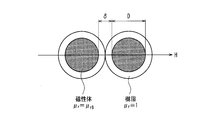
- FIG. 8 shows a simulation model for which the result is shown in FIG.
- the magnetic permeability mu r of the entire radio wave absorbing layer can be expressed by the following equation (3).
- the volume content of the magnetic powder shown in the radio wave absorption layer can be expressed as the above formula (4) from the relationship between the diameter D and ⁇ .
- Expression (5) can be derived from Expression (3) and Expression (4), the magnetic permeability real part ⁇ ′ and the magnetic permeability imaginary part ⁇ ′′ are obtained using Expression (5), respectively. This is shown in FIG.
- the volume content of epsilon iron oxide is preferably 30% or more in order to achieve a radio wave absorption degree of -15 dB or more and a radio wave absorption ratio of 90% or more. Further, it was found that if the volume content of epsilon iron oxide is 40% or more, it is preferable from the viewpoint of radio wave absorption performance, and further, if the volume content of epsilon iron oxide is 50% or more, it is more preferable.
- the radio wave absorption layer of this embodiment is formed by producing a magnetic paint as described above, applying and drying it, and then performing a calendar process.
- the volume content on the composition of the magnetic oxide at the time of production of the magnetic coating is 63.8%
- the porosity before the calendar treatment in the coated and dried state is about 27.5%
- the volume content of the actual magnetic iron oxide including the void portion as the radio wave absorption layer was 46.3%.
- the porosity was 18.6%
- the volume content of the actual magnetic iron oxide containing the voids was 51.9%.
- a radio wave absorption layer having a very high radio wave absorption level by magnetic resonance can be formed.
- the radio wave absorptivity is ⁇ 10 dB or more. If the volume content of the magnetic oxide is 30% or more, it is surely practical. A radio wave absorbing sheet having a radio wave absorption rate can be realized. Moreover, when the binder of a general material is used, if the volume content of magnetic iron oxide exceeds 80%, the flexibility as a radio wave absorbing sheet cannot be ensured.
- the volume content of the magnetic oxide in the radio wave absorption layer is preferably 30% or more, and the upper limit is about 80%. Further, it can be said that the volume content of the magnetic oxide in the radio wave absorption layer is more preferably 50% or more.
- the formation of the radio wave absorption layer is not limited to the above method using a solvent, and a method of forming a radio wave absorption material by dispersing and mixing it in a binder without using a solvent can be considered.
- a method of forming a radio wave absorption material by dispersing and mixing it in a binder without using a solvent can be considered.
- the gap of the radio wave absorption layer is smaller than that of the radio wave absorption layer produced using a solvent, even if the volume content of the radio wave absorption material contained in the radio wave absorption layer is small, good radio wave absorption characteristics Is believed to be secured.
- radio wave absorption sheet by using epsilon iron oxide that performs magnetic resonance in a high frequency band equal to or higher than the millimeter wave band as the radio wave absorbing material, frequencies from the millimeter wave band to 1 terahertz are used.
- a radio wave absorbing sheet that absorbs radio waves in a band can be realized.
- the radio wave absorbing material contained in the radio wave absorbing layer is described as an example using epsilon iron oxide.
- epsilon iron oxide it is possible to form a radio wave absorbing sheet that absorbs radio waves in the millimeter wave band of 30 GHz to 300 GHz, and further, rhodium as a metal material that replaces the Fe site.
- a radio wave absorbing sheet that absorbs 1 terahertz radio wave, which is the highest frequency defined as radio waves.
- the magnetic iron oxide used as the radio wave absorbing material of the radio wave absorbing layer is not limited to epsilon iron oxide.
- Hexagonal ferrite as a ferrite-based electromagnetic absorber exhibits radio wave absorption characteristics in the 76 gigahertz band, and strontium ferrite also exhibits radio wave absorption characteristics in the tens of gigahertz band.
- a radio wave absorption layer is formed by using magnetic iron oxide particles having radio wave absorption characteristics in such a millimeter wave band of 30 GHz to 300 GHz and a resin binder.
- a radio wave absorbing sheet that absorbs radio waves in the millimeter wave band can be realized.
- the hexagonal ferrite particles have an average particle size as large as about 10 ⁇ m as compared with the epsilon iron oxide particles exemplified in the above embodiment, and the particle shape is not substantially spherical but is a plate or needle. Crystal.
- the use of a dispersant and the conditions for kneading with the binder are adjusted so that the magnetic coating is applied as uniformly as possible in the electromagnetic wave absorption layer. It is preferable to adjust so that the porosity is as small as possible while the iron oxide powder is dispersed.
- magnetic iron oxide powder, a binder, and a dispersant as necessary are blended in advance, and these blended materials are supplied into a plastic cylinder from a resin supply port of an extruder.
- an extrusion molding machine a normal extrusion machine including a plastic cylinder, a die provided at the tip of the plastic cylinder, a screw rotatably disposed in the plastic cylinder, and a drive mechanism for driving the screw.
- a molding machine can be used.
- the molten material plasticized by the band heater of the extrusion molding machine is fed forward by the rotation of the screw and extruded from the tip into a sheet shape.
- a radio wave absorption layer having a predetermined thickness can be obtained by subjecting the extruded material to drying, pressure molding, calendering, and the like.
- the radio wave absorption sheet having a single radio wave absorption layer has been described.
- a radio wave absorption layer in which a plurality of layers are stacked can be used.
- the radio wave absorption sheet according to the present embodiment can further improve the radio wave absorption characteristics by adjusting the thickness of the radio wave absorption layer and matching the impedance with the impedance in the air.
- the radio wave absorption layer having a predetermined thickness cannot be formed by a single layer due to the characteristics of the radio wave absorption material or the binder forming the radio wave absorption layer, it is effective to form the radio wave absorption layer as a laminate.
- the radio wave absorption sheet disclosed in the present application is useful as a radio wave absorption sheet that absorbs radio waves in a high frequency band equal to or higher than the millimeter wave band.
- Radio wave absorption layer 1a Epsilon iron oxide (radio wave absorption material) 1b Binder 2 Reflecting layer 3 Base film (base material) 4 Adhesive layer
Landscapes
- Engineering & Computer Science (AREA)
- Chemical & Material Sciences (AREA)
- Dispersion Chemistry (AREA)
- Power Engineering (AREA)
- Microelectronics & Electronic Packaging (AREA)
- Shielding Devices Or Components To Electric Or Magnetic Fields (AREA)
- Soft Magnetic Materials (AREA)
- Laminated Bodies (AREA)
Priority Applications (3)
| Application Number | Priority Date | Filing Date | Title |
|---|---|---|---|
| US16/312,831 US20190215994A1 (en) | 2016-06-22 | 2017-06-21 | Electric wave absorption sheet |
| EP17815460.5A EP3478046A4 (de) | 2016-06-22 | 2017-06-21 | Elektrowellenabsorptionsfolie |
| JP2018502027A JP6764465B2 (ja) | 2016-06-22 | 2017-06-21 | 電波吸収シート |
Applications Claiming Priority (2)
| Application Number | Priority Date | Filing Date | Title |
|---|---|---|---|
| JP2016-123493 | 2016-06-22 | ||
| JP2016123493 | 2016-06-22 |
Publications (1)
| Publication Number | Publication Date |
|---|---|
| WO2017221992A1 true WO2017221992A1 (ja) | 2017-12-28 |
Family
ID=60783451
Family Applications (1)
| Application Number | Title | Priority Date | Filing Date |
|---|---|---|---|
| PCT/JP2017/022912 Ceased WO2017221992A1 (ja) | 2016-06-22 | 2017-06-21 | 電波吸収シート |
Country Status (4)
| Country | Link |
|---|---|
| US (1) | US20190215994A1 (de) |
| EP (1) | EP3478046A4 (de) |
| JP (2) | JP6764465B2 (de) |
| WO (1) | WO2017221992A1 (de) |
Cited By (8)
| Publication number | Priority date | Publication date | Assignee | Title |
|---|---|---|---|---|
| WO2019176612A1 (ja) * | 2018-03-12 | 2019-09-19 | マクセルホールディングス株式会社 | 電磁波吸収体用組成物、電磁波吸収体三次元造形物、それを用いた電子部品及び電子機器、並びにその電子部品及び電子機器の製造方法 |
| WO2019188351A1 (ja) * | 2018-03-28 | 2019-10-03 | マクセルホールディングス株式会社 | 電磁波吸収体 |
| JPWO2021029249A1 (de) * | 2019-08-09 | 2021-02-18 | ||
| EP3754673A4 (de) * | 2018-02-15 | 2021-12-08 | The University of Tokyo | Magnetisches material, verfahren zur herstellung davon und folie zur absorption elektromagnetischer wellen |
| JP2022058813A (ja) * | 2018-03-12 | 2022-04-12 | マクセル株式会社 | 実時間送受信装置 |
| WO2022168885A1 (ja) | 2021-02-04 | 2022-08-11 | マクセル株式会社 | 電波吸収体、および電波吸収装置 |
| JP2023132076A (ja) * | 2022-03-10 | 2023-09-22 | 国立研究開発法人情報通信研究機構 | 電波吸収体 |
| RU2836317C1 (ru) * | 2024-06-07 | 2025-03-12 | Общество с ограниченной ответственностью "Завод герметизирующих материалов" | Радиопоглощающий материал |
Families Citing this family (15)
| Publication number | Priority date | Publication date | Assignee | Title |
|---|---|---|---|---|
| EP3537861B1 (de) * | 2016-11-04 | 2022-03-30 | Maxell, Ltd. | Folie zum absorbieren elektromagnetischer wellen |
| WO2019077808A1 (ja) * | 2017-10-19 | 2019-04-25 | 関西ペイント株式会社 | ミリ波帯域用電波吸収シート及びミリ波電波吸収方法 |
| JP6461416B1 (ja) * | 2018-06-21 | 2019-01-30 | 清二 加川 | 電磁波吸収複合シート |
| JP6404522B1 (ja) * | 2018-07-03 | 2018-10-10 | 清二 加川 | 電磁波吸収複合シート |
| WO2020044706A1 (ja) | 2018-08-28 | 2020-03-05 | 富士フイルム株式会社 | マグネトプランバイト型六方晶フェライトの粉体及びその製造方法、並びに電波吸収体 |
| JP7496816B2 (ja) | 2019-05-14 | 2024-06-07 | 富士フイルム株式会社 | 電波吸収体及びコンパウンド |
| WO2020230680A1 (ja) | 2019-05-14 | 2020-11-19 | 富士フイルム株式会社 | 電波吸収体 |
| CN113812043B (zh) * | 2019-05-14 | 2023-12-01 | 富士胶片株式会社 | 电波吸收体 |
| EP3972402B1 (de) * | 2019-05-14 | 2025-04-09 | FUJIFILM Corporation | Funkwellenabsorber |
| JP2022536110A (ja) * | 2019-06-05 | 2022-08-12 | ビーエーエスエフ ソシエタス・ヨーロピア | 電磁波透過低減材料 |
| CN114271041B (zh) | 2019-08-09 | 2024-08-13 | 富士胶片株式会社 | 电波吸收性组合物及电波吸收体 |
| KR102705189B1 (ko) * | 2019-09-30 | 2024-09-11 | 후지필름 가부시키가이샤 | 전파 흡수체 및 전파 흡수성 조성물 |
| US12187459B2 (en) * | 2019-11-05 | 2025-01-07 | Institute For Q-Shu Pioneers Of Space, Inc. | Spacecraft |
| CN113321963A (zh) * | 2021-06-04 | 2021-08-31 | 宋京忠 | 一种飞机防雷达隐身材料及其制备方法 |
| CN113571919B (zh) * | 2021-07-07 | 2023-06-16 | 佛山(华南)新材料研究院 | 一种吸波器件及其制备方法 |
Citations (10)
| Publication number | Priority date | Publication date | Assignee | Title |
|---|---|---|---|---|
| JP2006080352A (ja) | 2004-09-10 | 2006-03-23 | Hitachi Chem Co Ltd | 電波吸収シート |
| JP2006332260A (ja) * | 2005-05-25 | 2006-12-07 | Hajime Murazaki | 電磁波遮蔽材及び電磁波遮蔽構造体 |
| JP2007193323A (ja) * | 2005-12-22 | 2007-08-02 | Fujifilm Corp | 反射防止フィルム、及びそれを用いたプラズマディスプレイパネル用前面板、プラズマディスプレイパネル表示装置、画像表示装置 |
| JP2008060484A (ja) | 2006-09-01 | 2008-03-13 | Univ Of Tokyo | 電波吸収性磁性結晶および電波吸収体 |
| JP2009059752A (ja) * | 2007-08-30 | 2009-03-19 | Hitachi Chem Co Ltd | 難燃化ノイズ抑制シート |
| JP2011181679A (ja) * | 2010-03-01 | 2011-09-15 | Tdk Corp | 電磁波吸収シート及びその製造方法 |
| JP2011233834A (ja) | 2010-04-30 | 2011-11-17 | Shachihata Inc | 電波吸収体 |
| JP2012071596A (ja) * | 2010-09-02 | 2012-04-12 | Nippon Steel Corp | 導電性、耐食性に優れる塗装金属板 |
| JP2015198163A (ja) | 2014-04-01 | 2015-11-09 | 株式会社リケン | 近傍界用電波吸収シート |
| JP2016111341A (ja) * | 2014-12-03 | 2016-06-20 | 国立大学法人 東京大学 | 電磁波吸収体及び膜形成用ペースト |
Family Cites Families (11)
| Publication number | Priority date | Publication date | Assignee | Title |
|---|---|---|---|---|
| JP4790892B2 (ja) * | 2000-04-27 | 2011-10-12 | ポリマテック株式会社 | 電波吸収体 |
| JP2006032929A (ja) * | 2004-06-14 | 2006-02-02 | Nitta Ind Corp | 電磁干渉抑制体、これを用いる電磁障害抑制方法、およびrf‐idデバイス |
| JP2006156561A (ja) * | 2004-11-26 | 2006-06-15 | Komatsu Seiren Co Ltd | 電磁波シールド材及びその製造方法 |
| JP2006310575A (ja) * | 2005-04-28 | 2006-11-09 | Konica Minolta Photo Imaging Inc | 電磁波吸収転写箔及び電磁波吸収転写箔の付与方法 |
| JP4859791B2 (ja) * | 2006-09-01 | 2012-01-25 | 国立大学法人 東京大学 | 電波吸収材料用の磁性結晶および電波吸収体 |
| WO2010150853A1 (ja) * | 2009-06-24 | 2010-12-29 | 国立大学法人東京大学 | 磁性薄膜の製造方法、磁性薄膜及び磁性体 |
| JP6089625B2 (ja) * | 2011-11-30 | 2017-03-08 | 東レ株式会社 | 電波吸収体用シート材およびこれを用いた電波吸収体 |
| US9411076B2 (en) * | 2012-09-14 | 2016-08-09 | Ppg Industries Ohio, Inc. | Pigmented polymerizable compositions and optical articles prepared therefrom |
| JP2014192327A (ja) * | 2013-03-27 | 2014-10-06 | Riken Corp | 近傍界用電波吸収シートおよびその製造方法 |
| JP2015220259A (ja) * | 2014-05-14 | 2015-12-07 | Tdk株式会社 | 磁気抑制シート及びその製造方法 |
| EP3029771B1 (de) * | 2014-12-03 | 2019-10-16 | The University of Tokyo | Absorber für elektromagnetische wellen und filmbildende paste |
-
2017
- 2017-06-21 EP EP17815460.5A patent/EP3478046A4/de not_active Withdrawn
- 2017-06-21 JP JP2018502027A patent/JP6764465B2/ja active Active
- 2017-06-21 WO PCT/JP2017/022912 patent/WO2017221992A1/ja not_active Ceased
- 2017-06-21 US US16/312,831 patent/US20190215994A1/en not_active Abandoned
-
2019
- 2019-07-01 JP JP2019122904A patent/JP2019195083A/ja active Pending
Patent Citations (10)
| Publication number | Priority date | Publication date | Assignee | Title |
|---|---|---|---|---|
| JP2006080352A (ja) | 2004-09-10 | 2006-03-23 | Hitachi Chem Co Ltd | 電波吸収シート |
| JP2006332260A (ja) * | 2005-05-25 | 2006-12-07 | Hajime Murazaki | 電磁波遮蔽材及び電磁波遮蔽構造体 |
| JP2007193323A (ja) * | 2005-12-22 | 2007-08-02 | Fujifilm Corp | 反射防止フィルム、及びそれを用いたプラズマディスプレイパネル用前面板、プラズマディスプレイパネル表示装置、画像表示装置 |
| JP2008060484A (ja) | 2006-09-01 | 2008-03-13 | Univ Of Tokyo | 電波吸収性磁性結晶および電波吸収体 |
| JP2009059752A (ja) * | 2007-08-30 | 2009-03-19 | Hitachi Chem Co Ltd | 難燃化ノイズ抑制シート |
| JP2011181679A (ja) * | 2010-03-01 | 2011-09-15 | Tdk Corp | 電磁波吸収シート及びその製造方法 |
| JP2011233834A (ja) | 2010-04-30 | 2011-11-17 | Shachihata Inc | 電波吸収体 |
| JP2012071596A (ja) * | 2010-09-02 | 2012-04-12 | Nippon Steel Corp | 導電性、耐食性に優れる塗装金属板 |
| JP2015198163A (ja) | 2014-04-01 | 2015-11-09 | 株式会社リケン | 近傍界用電波吸収シート |
| JP2016111341A (ja) * | 2014-12-03 | 2016-06-20 | 国立大学法人 東京大学 | 電磁波吸収体及び膜形成用ペースト |
Non-Patent Citations (1)
| Title |
|---|
| See also references of EP3478046A4 |
Cited By (14)
| Publication number | Priority date | Publication date | Assignee | Title |
|---|---|---|---|---|
| EP3754673A4 (de) * | 2018-02-15 | 2021-12-08 | The University of Tokyo | Magnetisches material, verfahren zur herstellung davon und folie zur absorption elektromagnetischer wellen |
| JP7141444B2 (ja) | 2018-03-12 | 2022-09-22 | マクセル株式会社 | 電磁波吸収体用組成物、電磁波吸収体三次元造形物、それを用いた電子部品及び電子機器、並びにその電子部品及び電子機器の製造方法 |
| TWI843719B (zh) * | 2018-03-12 | 2024-06-01 | 日商麥克賽爾股份有限公司 | 電磁波吸收體用組成物、電磁波吸收體三維造形物、使用其的電子部件及電子機器、以及其電子部件及電子機器的製造方法 |
| WO2019176612A1 (ja) * | 2018-03-12 | 2019-09-19 | マクセルホールディングス株式会社 | 電磁波吸収体用組成物、電磁波吸収体三次元造形物、それを用いた電子部品及び電子機器、並びにその電子部品及び電子機器の製造方法 |
| JPWO2019176612A1 (ja) * | 2018-03-12 | 2021-03-25 | マクセルホールディングス株式会社 | 電磁波吸収体用組成物、電磁波吸収体三次元造形物、それを用いた電子部品及び電子機器、並びにその電子部品及び電子機器の製造方法 |
| JP2022058813A (ja) * | 2018-03-12 | 2022-04-12 | マクセル株式会社 | 実時間送受信装置 |
| WO2019188351A1 (ja) * | 2018-03-28 | 2019-10-03 | マクセルホールディングス株式会社 | 電磁波吸収体 |
| WO2021029249A1 (ja) * | 2019-08-09 | 2021-02-18 | 富士フイルム株式会社 | 電波吸収性組成物および電波吸収体 |
| JPWO2021029249A1 (de) * | 2019-08-09 | 2021-02-18 | ||
| WO2022168885A1 (ja) | 2021-02-04 | 2022-08-11 | マクセル株式会社 | 電波吸収体、および電波吸収装置 |
| EP4290995A4 (de) * | 2021-02-04 | 2025-01-01 | Maxell, Ltd. | Funkwellenabsorber und funkwellenabsorbervorrichtung |
| JP2023132076A (ja) * | 2022-03-10 | 2023-09-22 | 国立研究開発法人情報通信研究機構 | 電波吸収体 |
| RU2836317C1 (ru) * | 2024-06-07 | 2025-03-12 | Общество с ограниченной ответственностью "Завод герметизирующих материалов" | Радиопоглощающий материал |
| RU2846079C1 (ru) * | 2025-03-17 | 2025-08-29 | Общество с ограниченной ответственностью "Завод герметизирующих материалов" | Эластомерный радиопоглощающий материал |
Also Published As
| Publication number | Publication date |
|---|---|
| JP2019195083A (ja) | 2019-11-07 |
| JP6764465B2 (ja) | 2020-09-30 |
| JPWO2017221992A1 (ja) | 2018-09-27 |
| US20190215994A1 (en) | 2019-07-11 |
| EP3478046A1 (de) | 2019-05-01 |
| EP3478046A4 (de) | 2020-02-19 |
Similar Documents
| Publication | Publication Date | Title |
|---|---|---|
| JP2019195083A (ja) | 電波吸収シート | |
| JP7688754B2 (ja) | 電磁波吸収体、および電磁波吸収体の製造方法 | |
| JP6445741B2 (ja) | 電磁波吸収シート | |
| JP6454445B2 (ja) | 電磁波吸収シート | |
| JPWO2018235952A1 (ja) | 電磁波吸収性組成物、電磁波吸収シート | |
| JP2018056492A (ja) | 電波吸収シート | |
| JP7751708B2 (ja) | 電磁波吸収体 | |
| JP2023067902A (ja) | 電磁波吸収体用組成物、および、電磁波吸収体 | |
| TWI787517B (zh) | 電磁波吸收體及電磁波吸收體用組成物 | |
| WO2022168885A1 (ja) | 電波吸収体、および電波吸収装置 |
Legal Events
| Date | Code | Title | Description |
|---|---|---|---|
| ENP | Entry into the national phase |
Ref document number: 2018502027 Country of ref document: JP Kind code of ref document: A |
|
| 121 | Ep: the epo has been informed by wipo that ep was designated in this application |
Ref document number: 17815460 Country of ref document: EP Kind code of ref document: A1 |
|
| NENP | Non-entry into the national phase |
Ref country code: DE |
|
| ENP | Entry into the national phase |
Ref document number: 2017815460 Country of ref document: EP Effective date: 20190122 |