WO2018010180A1 - Oscillateur - Google Patents
Oscillateur Download PDFInfo
- Publication number
- WO2018010180A1 WO2018010180A1 PCT/CN2016/090223 CN2016090223W WO2018010180A1 WO 2018010180 A1 WO2018010180 A1 WO 2018010180A1 CN 2016090223 W CN2016090223 W CN 2016090223W WO 2018010180 A1 WO2018010180 A1 WO 2018010180A1
- Authority
- WO
- WIPO (PCT)
- Prior art keywords
- mos transistor
- capacitor
- unit
- oscillator
- pole
- Prior art date
- Legal status (The legal status is an assumption and is not a legal conclusion. Google has not performed a legal analysis and makes no representation as to the accuracy of the status listed.)
- Ceased
Links
Images




Classifications
-
- H—ELECTRICITY
- H03—ELECTRONIC CIRCUITRY
- H03K—PULSE TECHNIQUE
- H03K3/00—Circuits for generating electric pulses; Monostable, bistable or multistable circuits
- H03K3/02—Generators characterised by the type of circuit or by the means used for producing pulses
- H03K3/023—Generators characterised by the type of circuit or by the means used for producing pulses by the use of differential amplifiers or comparators, with internal or external positive feedback
- H03K3/0233—Bistable circuits
- H03K3/02335—Bistable circuits provided with means for increasing reliability; for protection; for ensuring a predetermined initial state when the supply voltage has been applied; for storing the actual state when the supply voltage fails
-
- H—ELECTRICITY
- H03—ELECTRONIC CIRCUITRY
- H03B—GENERATION OF OSCILLATIONS, DIRECTLY OR BY FREQUENCY-CHANGING, BY CIRCUITS EMPLOYING ACTIVE ELEMENTS WHICH OPERATE IN A NON-SWITCHING MANNER; GENERATION OF NOISE BY SUCH CIRCUITS
- H03B5/00—Generation of oscillations using amplifier with regenerative feedback from output to input
- H03B5/08—Generation of oscillations using amplifier with regenerative feedback from output to input with frequency-determining element comprising lumped inductance and capacitance
- H03B5/12—Generation of oscillations using amplifier with regenerative feedback from output to input with frequency-determining element comprising lumped inductance and capacitance active element in amplifier being semiconductor device
- H03B5/1237—Generation of oscillations using amplifier with regenerative feedback from output to input with frequency-determining element comprising lumped inductance and capacitance active element in amplifier being semiconductor device comprising means for varying the frequency of the generator
- H03B5/124—Generation of oscillations using amplifier with regenerative feedback from output to input with frequency-determining element comprising lumped inductance and capacitance active element in amplifier being semiconductor device comprising means for varying the frequency of the generator the means comprising a voltage dependent capacitance
- H03B5/1243—Generation of oscillations using amplifier with regenerative feedback from output to input with frequency-determining element comprising lumped inductance and capacitance active element in amplifier being semiconductor device comprising means for varying the frequency of the generator the means comprising a voltage dependent capacitance the means comprising voltage variable capacitance diodes
-
- H—ELECTRICITY
- H03—ELECTRONIC CIRCUITRY
- H03B—GENERATION OF OSCILLATIONS, DIRECTLY OR BY FREQUENCY-CHANGING, BY CIRCUITS EMPLOYING ACTIVE ELEMENTS WHICH OPERATE IN A NON-SWITCHING MANNER; GENERATION OF NOISE BY SUCH CIRCUITS
- H03B5/00—Generation of oscillations using amplifier with regenerative feedback from output to input
- H03B5/08—Generation of oscillations using amplifier with regenerative feedback from output to input with frequency-determining element comprising lumped inductance and capacitance
- H03B5/12—Generation of oscillations using amplifier with regenerative feedback from output to input with frequency-determining element comprising lumped inductance and capacitance active element in amplifier being semiconductor device
- H03B5/1206—Generation of oscillations using amplifier with regenerative feedback from output to input with frequency-determining element comprising lumped inductance and capacitance active element in amplifier being semiconductor device using multiple transistors for amplification
- H03B5/1212—Generation of oscillations using amplifier with regenerative feedback from output to input with frequency-determining element comprising lumped inductance and capacitance active element in amplifier being semiconductor device using multiple transistors for amplification the amplifier comprising a pair of transistors, wherein an output terminal of each being connected to an input terminal of the other, e.g. a cross coupled pair
-
- H—ELECTRICITY
- H03—ELECTRONIC CIRCUITRY
- H03B—GENERATION OF OSCILLATIONS, DIRECTLY OR BY FREQUENCY-CHANGING, BY CIRCUITS EMPLOYING ACTIVE ELEMENTS WHICH OPERATE IN A NON-SWITCHING MANNER; GENERATION OF NOISE BY SUCH CIRCUITS
- H03B5/00—Generation of oscillations using amplifier with regenerative feedback from output to input
- H03B5/08—Generation of oscillations using amplifier with regenerative feedback from output to input with frequency-determining element comprising lumped inductance and capacitance
- H03B5/12—Generation of oscillations using amplifier with regenerative feedback from output to input with frequency-determining element comprising lumped inductance and capacitance active element in amplifier being semiconductor device
- H03B5/1206—Generation of oscillations using amplifier with regenerative feedback from output to input with frequency-determining element comprising lumped inductance and capacitance active element in amplifier being semiconductor device using multiple transistors for amplification
- H03B5/1212—Generation of oscillations using amplifier with regenerative feedback from output to input with frequency-determining element comprising lumped inductance and capacitance active element in amplifier being semiconductor device using multiple transistors for amplification the amplifier comprising a pair of transistors, wherein an output terminal of each being connected to an input terminal of the other, e.g. a cross coupled pair
- H03B5/1215—Generation of oscillations using amplifier with regenerative feedback from output to input with frequency-determining element comprising lumped inductance and capacitance active element in amplifier being semiconductor device using multiple transistors for amplification the amplifier comprising a pair of transistors, wherein an output terminal of each being connected to an input terminal of the other, e.g. a cross coupled pair the current source or degeneration circuit being in common to both transistors of the pair, e.g. a cross-coupled long-tailed pair
-
- H—ELECTRICITY
- H03—ELECTRONIC CIRCUITRY
- H03B—GENERATION OF OSCILLATIONS, DIRECTLY OR BY FREQUENCY-CHANGING, BY CIRCUITS EMPLOYING ACTIVE ELEMENTS WHICH OPERATE IN A NON-SWITCHING MANNER; GENERATION OF NOISE BY SUCH CIRCUITS
- H03B5/00—Generation of oscillations using amplifier with regenerative feedback from output to input
- H03B5/08—Generation of oscillations using amplifier with regenerative feedback from output to input with frequency-determining element comprising lumped inductance and capacitance
- H03B5/12—Generation of oscillations using amplifier with regenerative feedback from output to input with frequency-determining element comprising lumped inductance and capacitance active element in amplifier being semiconductor device
- H03B5/1228—Generation of oscillations using amplifier with regenerative feedback from output to input with frequency-determining element comprising lumped inductance and capacitance active element in amplifier being semiconductor device the amplifier comprising one or more field effect transistors
-
- H—ELECTRICITY
- H03—ELECTRONIC CIRCUITRY
- H03B—GENERATION OF OSCILLATIONS, DIRECTLY OR BY FREQUENCY-CHANGING, BY CIRCUITS EMPLOYING ACTIVE ELEMENTS WHICH OPERATE IN A NON-SWITCHING MANNER; GENERATION OF NOISE BY SUCH CIRCUITS
- H03B5/00—Generation of oscillations using amplifier with regenerative feedback from output to input
- H03B5/08—Generation of oscillations using amplifier with regenerative feedback from output to input with frequency-determining element comprising lumped inductance and capacitance
- H03B5/12—Generation of oscillations using amplifier with regenerative feedback from output to input with frequency-determining element comprising lumped inductance and capacitance active element in amplifier being semiconductor device
- H03B5/1237—Generation of oscillations using amplifier with regenerative feedback from output to input with frequency-determining element comprising lumped inductance and capacitance active element in amplifier being semiconductor device comprising means for varying the frequency of the generator
- H03B5/1262—Generation of oscillations using amplifier with regenerative feedback from output to input with frequency-determining element comprising lumped inductance and capacitance active element in amplifier being semiconductor device comprising means for varying the frequency of the generator the means comprising switched elements
- H03B5/1265—Generation of oscillations using amplifier with regenerative feedback from output to input with frequency-determining element comprising lumped inductance and capacitance active element in amplifier being semiconductor device comprising means for varying the frequency of the generator the means comprising switched elements switched capacitors
-
- H—ELECTRICITY
- H03—ELECTRONIC CIRCUITRY
- H03B—GENERATION OF OSCILLATIONS, DIRECTLY OR BY FREQUENCY-CHANGING, BY CIRCUITS EMPLOYING ACTIVE ELEMENTS WHICH OPERATE IN A NON-SWITCHING MANNER; GENERATION OF NOISE BY SUCH CIRCUITS
- H03B7/00—Generation of oscillations using active element having a negative resistance between two of its electrodes
- H03B7/02—Generation of oscillations using active element having a negative resistance between two of its electrodes with frequency-determining element comprising lumped inductance and capacitance
- H03B7/06—Generation of oscillations using active element having a negative resistance between two of its electrodes with frequency-determining element comprising lumped inductance and capacitance active element being semiconductor device
-
- H—ELECTRICITY
- H03—ELECTRONIC CIRCUITRY
- H03K—PULSE TECHNIQUE
- H03K3/00—Circuits for generating electric pulses; Monostable, bistable or multistable circuits
- H03K3/01—Details
- H03K3/011—Modifications of generator to compensate for variations in physical values, e.g. voltage, temperature
-
- H—ELECTRICITY
- H03—ELECTRONIC CIRCUITRY
- H03K—PULSE TECHNIQUE
- H03K3/00—Circuits for generating electric pulses; Monostable, bistable or multistable circuits
- H03K3/01—Details
- H03K3/012—Modifications of generator to improve response time or to decrease power consumption
-
- H—ELECTRICITY
- H03—ELECTRONIC CIRCUITRY
- H03K—PULSE TECHNIQUE
- H03K3/00—Circuits for generating electric pulses; Monostable, bistable or multistable circuits
- H03K3/01—Details
- H03K3/013—Modifications of generator to prevent operation by noise or interference
-
- H—ELECTRICITY
- H03—ELECTRONIC CIRCUITRY
- H03L—AUTOMATIC CONTROL, STARTING, SYNCHRONISATION OR STABILISATION OF GENERATORS OF ELECTRONIC OSCILLATIONS OR PULSES
- H03L7/00—Automatic control of frequency or phase; Synchronisation
- H03L7/06—Automatic control of frequency or phase; Synchronisation using a reference signal applied to a frequency- or phase-locked loop
- H03L7/08—Details of the phase-locked loop
- H03L7/099—Details of the phase-locked loop concerning mainly the controlled oscillator of the loop
-
- H—ELECTRICITY
- H04—ELECTRIC COMMUNICATION TECHNIQUE
- H04B—TRANSMISSION
- H04B5/00—Near-field transmission systems, e.g. inductive or capacitive transmission systems
- H04B5/20—Near-field transmission systems, e.g. inductive or capacitive transmission systems characterised by the transmission technique; characterised by the transmission medium
- H04B5/24—Inductive coupling
-
- H—ELECTRICITY
- H03—ELECTRONIC CIRCUITRY
- H03B—GENERATION OF OSCILLATIONS, DIRECTLY OR BY FREQUENCY-CHANGING, BY CIRCUITS EMPLOYING ACTIVE ELEMENTS WHICH OPERATE IN A NON-SWITCHING MANNER; GENERATION OF NOISE BY SUCH CIRCUITS
- H03B2200/00—Indexing scheme relating to details of oscillators covered by H03B
- H03B2200/0002—Types of oscillators
- H03B2200/0008—Colpitts oscillator
-
- H—ELECTRICITY
- H03—ELECTRONIC CIRCUITRY
- H03B—GENERATION OF OSCILLATIONS, DIRECTLY OR BY FREQUENCY-CHANGING, BY CIRCUITS EMPLOYING ACTIVE ELEMENTS WHICH OPERATE IN A NON-SWITCHING MANNER; GENERATION OF NOISE BY SUCH CIRCUITS
- H03B2200/00—Indexing scheme relating to details of oscillators covered by H03B
- H03B2200/003—Circuit elements of oscillators
- H03B2200/004—Circuit elements of oscillators including a variable capacitance, e.g. a varicap, a varactor or a variable capacitance of a diode or transistor
-
- H—ELECTRICITY
- H03—ELECTRONIC CIRCUITRY
- H03B—GENERATION OF OSCILLATIONS, DIRECTLY OR BY FREQUENCY-CHANGING, BY CIRCUITS EMPLOYING ACTIVE ELEMENTS WHICH OPERATE IN A NON-SWITCHING MANNER; GENERATION OF NOISE BY SUCH CIRCUITS
- H03B2200/00—Indexing scheme relating to details of oscillators covered by H03B
- H03B2200/003—Circuit elements of oscillators
- H03B2200/005—Circuit elements of oscillators including measures to switch a capacitor
-
- H—ELECTRICITY
- H03—ELECTRONIC CIRCUITRY
- H03B—GENERATION OF OSCILLATIONS, DIRECTLY OR BY FREQUENCY-CHANGING, BY CIRCUITS EMPLOYING ACTIVE ELEMENTS WHICH OPERATE IN A NON-SWITCHING MANNER; GENERATION OF NOISE BY SUCH CIRCUITS
- H03B2200/00—Indexing scheme relating to details of oscillators covered by H03B
- H03B2200/003—Circuit elements of oscillators
- H03B2200/0058—Circuit elements of oscillators with particular transconductance characteristics, e.g. an operational transconductance amplifier
-
- H—ELECTRICITY
- H03—ELECTRONIC CIRCUITRY
- H03B—GENERATION OF OSCILLATIONS, DIRECTLY OR BY FREQUENCY-CHANGING, BY CIRCUITS EMPLOYING ACTIVE ELEMENTS WHICH OPERATE IN A NON-SWITCHING MANNER; GENERATION OF NOISE BY SUCH CIRCUITS
- H03B2200/00—Indexing scheme relating to details of oscillators covered by H03B
- H03B2200/006—Functional aspects of oscillators
- H03B2200/0062—Bias and operating point
-
- H—ELECTRICITY
- H03—ELECTRONIC CIRCUITRY
- H03B—GENERATION OF OSCILLATIONS, DIRECTLY OR BY FREQUENCY-CHANGING, BY CIRCUITS EMPLOYING ACTIVE ELEMENTS WHICH OPERATE IN A NON-SWITCHING MANNER; GENERATION OF NOISE BY SUCH CIRCUITS
- H03B2200/00—Indexing scheme relating to details of oscillators covered by H03B
- H03B2200/006—Functional aspects of oscillators
- H03B2200/0088—Reduction of noise
- H03B2200/009—Reduction of phase noise
-
- H—ELECTRICITY
- H04—ELECTRIC COMMUNICATION TECHNIQUE
- H04W—WIRELESS COMMUNICATION NETWORKS
- H04W88/00—Devices specially adapted for wireless communication networks, e.g. terminals, base stations or access point devices
- H04W88/08—Access point devices
Definitions
- Embodiments of the present invention relate to the field of electronic technologies, and in particular, to an oscillator.
- the oscillator has a wide range of applications.
- the power consumption and phase noise of the oscillator are the main parameters for measuring the performance of the oscillator, so oscillators with low power consumption and low phase noise have been the subject of long-term research.
- the oscillator includes a resonant unit 10 and a cross-complementary active connected to the resonant unit 10.
- Unit 11 the resonance unit 10 is for generating an oscillation signal having a certain oscillation frequency; the cross-complementary active unit 11 is for compensating for the energy consumption of the resonance unit 10, so that the resonance unit 10 outputs a stable oscillation signal.
- phase noise calculation formula of the oscillator is:
- ⁇ represents the frequency offset of the carrier processed or generated by the oscillator
- q max represents the maximum amount of charge of the current noise source.
- ⁇ ( ⁇ t) is ISF (Impulse Sensitivity Function), ⁇ ( ⁇ t) is NMF (Noise-modulating Function) whose phase changes with time.
- ISF describes that at some point in time, at some point The degree of shift in the phase of the output signal caused by the injection of a unit pulse current on each node. Since the waveform of the oscillating signal generated by the Cross-coupled negative-resistance oscillator shown in FIG. 1a is a sine wave, the unit pulse current is injected into the Cross-coupled negative-resistance oscillator at different time points, and then simulation is performed.
- Figure 1b shows the ISF eff of the Cross-coupled negative-resistance oscillator (ie, ⁇ eff ( ⁇ t) in equation (2)). It can be seen from Fig. 1b that the value of ISF eff is only ⁇ /2 time period (ie 3 ⁇ /2 to 2 ⁇ ) in one oscillation period (2 ⁇ ) is 0, and the remaining 3 ⁇ /2 time period (ie 0 to 3 ⁇ /2) None are 0. Therefore, combining equations (1) and (2), the phase noise of the Cross-coupled negative-resistance oscillator is relatively large in one oscillation period. Therefore, the phase noise performance of the Cross-coupled negative-resistance oscillator is relatively poor.
- Embodiments of the present invention provide an oscillator capable of achieving performance requirements of low power consumption.
- an embodiment of the present invention provides a low power consumption low phase noise oscillator, including: a resonant unit, a cross-coupled current source unit, and a positive feedback unit coupled between the current source unit and the resonant unit; a resonant unit for generating a differential oscillating signal having a first oscillating frequency; the positive feedback unit for receiving the differential oscillating signal, and performing gain enhancement on the differential oscillating signal to obtain a differential output oscillating signal; and a current source unit for An adjustable bias current is provided for the resonant unit and the positive feedback unit described above.
- Embodiments of the present invention provide an oscillator, wherein a current source unit can provide a tunable bias current for a positive feedback unit and a resonance unit, and a Gm-boosted structure with a positive feedback unit, so that the positive feedback unit can
- the gain enhancement is performed on the received differential oscillating signal to obtain a differential output oscillating signal. Therefore, the power consumption of the oscillator provided by the embodiment of the present invention can be reduced by reducing the bias current under the condition that the oscillator is normally started.
- the foregoing resonating unit is further configured to output a differential oscillating signal to the current source unit via a positive feedback unit; the current source unit is further configured to be used according to the resonating unit
- the differential oscillating signal is output, and the bias current is adjusted by controlling the magnitude of the bias voltage to adjust the amplitude of the differential output oscillating signal.
- the foregoing positive feedback unit includes: a first MOS (metal oxide semiconductor, Metal-Oxide- a transistor, a second MOS transistor, a first capacitor, a second capacitor, a third capacitor, and a fourth capacitor; wherein the first pole of the first MOS transistor As a first output node, respectively connected to the resonant unit and one end of the first capacitor, the second pole of the first MOS transistor is respectively connected to the other end of the first capacitor and one end of the third capacitor, the gate of the first MOS transistor and the first The gates of the two MOS transistors are connected to the first constant voltage source, and the first poles of the second MOS transistors are respectively connected as the second output node to one ends of the resonant unit and the second capacitor, and the second poles of the second MOS transistors are respectively The other end of the second capacitor is connected to one end of the fourth capacitor, the other end of the fourth capacitor is connected
- a forward differential signal output end is disposed between one end of the three capacitor and the third output node of the current source unit, and a negative differential signal output end is disposed between one end of the fourth capacitor and the fourth output node of the current source unit . This can reduce the effect of the output load on the forward differential oscillating signal and the negative differential oscillating signal.
- the first constant voltage source is a first power source.
- the resonating unit includes: a first inductor, a second An inductor and a switched capacitor array; wherein one end of the first inductor is connected to one end of the second inductor, and the other end of the first inductor is respectively connected to one end of the switched capacitor array and the first output node of the positive feedback unit; One end is respectively connected to the other end of the switched capacitor array and the second output node of the positive feedback unit, and one end of the first inductor and one end of the second inductor are connected to the first constant voltage node.
- the frequency value of the oscillator can be changed by opening or closing the switch in the array of capacitive switches.
- the current source unit includes: a third MOS transistor, a fourth MOS transistor, a fifth capacitor, and a sixth capacitor a first resistor and a second resistor; wherein a gate of the third MOS transistor is respectively connected to one end of the sixth capacitor and one end of the first resistor, and the drain of the third MOS transistor serves as a third output node and a fifth capacitor respectively One end is connected to one end of the third capacitor; the gate of the fourth MOS transistor is respectively connected to the other end of the fifth capacitor and one end of the second resistor, and the drain of the fourth MOS transistor serves as a fourth output node and a sixth capacitor respectively The other end of the fourth capacitor is connected to one end of the fourth capacitor; the other end of the first resistor and the other end of the second resistor are connected to an adjustable power supply for providing an adjustable bias voltage, current for the current source unit Source unit Specifically, the tunable bias current is provided to the resonant
- the third MOS transistor and the fourth MOS transistor in the oscillator are adjusted to different working modes, which can effectively reduce the first MOS transistor, the second MOS transistor, and the third in the oscillator.
- the MOS transistor and the fourth MOS transistor are turned on, when the startup gain in the oscillator is constant, since the on-times of the first MOS transistor, the second MOS transistor, the third MOS transistor, and the fourth MOS transistor become smaller, The current value in one oscillation period is reduced, and since the power consumption is proportional to the current, the power consumption of the oscillator is reduced.
- the third MOS transistor and the fourth MOS transistor are In the NMOS transistor, the first pole of the first MOS transistor and the first pole of the second MOS transistor are both drains, and the second pole of the first MOS transistor and the second pole of the second MOS transistor are both sources;
- the first constant voltage node is the first power source and the second constant voltage node is the ground.
- a seventh possible implementation manner of the first aspect when the first MOS transistor and the second MOS transistor are a PMOS transistor, a third MOS transistor, and a fourth MOS transistor
- the first pole of the first MOS transistor and the first pole of the second MOS transistor are both drains, and the second pole of the first MOS transistor and the second pole of the second MOS transistor are both sources
- the first constant voltage node is ground and the second constant voltage node is the first power source.
- the third MOS transistor and the fourth MOS transistor are In the NMOS transistor, the first pole of the first MOS transistor and the first pole of the second MOS transistor are both sources, and the second pole of the first MOS transistor and the second pole of the second MOS transistor are both drains;
- the constant voltage node is the first power source and the second constant voltage node is the ground.
- the first MOS transistor and the second MOS transistor are an NMOS transistor, a third MOS transistor, and a fourth
- the MOS transistor is a PMOS transistor
- the first pole of the first MOS transistor and the first pole of the second MOS transistor are both a source, a second pole of the first MOS transistor and a second pole of the second MOS transistor All are drains; the first constant voltage node is ground, and the second constant voltage node is a first power source.
- the switched capacitor The array includes at least one capacitive switch branch; any of the capacitive switch branches includes a seventh capacitor, a switch, and an eighth capacitor, wherein one end of the seventh capacitor is connected to the other end of the first inductor and the first output node of the positive feedback unit, The other end of the eighth capacitor is connected to the second output node of the positive feedback unit and the other end of the second inductor.
- the seventh capacitor and the eighth capacitor are adjustable capacitors.
- the embodiment of the present invention provides a terminal, where the terminal includes at least the short-distance communication device and the oscillation described in any one of the possible implementation manners of the first aspect to the eleventh possible implementation manner of the first aspect.
- the oscillator is used to provide a local carrier signal for the short-range communication device described above.
- an embodiment of the present invention provides a base station, where the base station includes at least a transceiver and a phase-locked loop circuit, and the first aspect of the phase-locked loop circuit is any one of the eleventh possible implementation manners of the first aspect.
- a possible implementation is the oscillator described to provide a local carrier signal for the transceiver described above.
- 1a is a schematic structural diagram of a Cross-coupled negative resistance oscillator provided in the prior art
- 1b is a graph showing a simulated ISF function of a Cross-coupled negative-resistance oscillator provided in the prior art
- FIG. 2 is a schematic structural diagram 1 of an oscillator according to an embodiment of the present invention.
- FIG. 3 is a schematic structural diagram 2 of an oscillator according to an embodiment of the present invention.
- 4a is a schematic structural diagram 3 of an oscillator according to an embodiment of the present invention.
- 4b is a current waveform diagram of a MOS transistor in a Cross-coupled negative-resistance oscillator provided by the prior art
- 4c is a current waveform diagram of a MOS transistor in an oscillator according to an embodiment of the present invention.
- FIG. 5 is a schematic structural diagram 4 of an oscillator according to an embodiment of the present disclosure.
- FIG. 6 is a schematic structural diagram 5 of an oscillator according to an embodiment of the present disclosure.
- FIG. 7 is a schematic structural diagram 6 of an oscillator according to an embodiment of the present disclosure.
- FIG. 8 is a schematic structural diagram 7 of an oscillator according to an embodiment of the present disclosure.
- FIG. 9 is a schematic structural diagram 10 of an oscillator according to an embodiment of the present disclosure.
- FIG. 10 is a schematic structural diagram 11 of an oscillator according to an embodiment of the present invention.
- FIG. 11 is a graph showing a simulated ISF function of an oscillator according to an embodiment of the present invention.
- Each of the MOS tubes in any embodiment or the accompanying drawings may be a single MOS tube that satisfies the required starting gain or the required on-current.
- the MOS tube combination that needs to meet the required starting gain or the required on-current according to the parallel combination of the plurality of MOS tubes, that is, the sum of the starting gains of each of the plurality of MOS tubes is greater than or equal to
- Each of the capacitors in the embodiment of the present invention may be a capacitor that satisfies a required capacitance value, or a capacitor combination that is composed of a plurality of capacitors in parallel or in series to satisfy a required capacitance value, that is, The plurality of capacitors are connected in series or in parallel, and the corresponding capacitor value is equal to the required capacitor value.
- Each inductor in the embodiment of the present invention may be an inductor that satisfies the required inductor value, or may be connected by multiple inductors in series or in
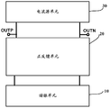
- an embodiment of the present invention provides an oscillator including a resonating unit 10, a cross-coupled current source unit 30, and a positive feedback unit 20 coupled between the current source unit 30 and the resonating unit 10;
- the resonant unit 10 is configured to generate a first oscillation frequency
- the differential oscillating signal 20 is configured to receive the differential oscillating signal and perform gain enhancement on the differential oscillating signal to obtain a differential output oscillating signal;
- the current source unit 30 is configured to provide an adjustable tunable unit 10 and the positive feedback unit 20 Bias current.
- a differential oscillation signal output terminal ie, a forward differential oscillation signal output terminal OUTP and a negative differential oscillation signal output terminal OUTN shown in FIG.
- the current source unit 30 provides the tunable bias current to the resonant unit 10 through the positive feedback unit 20.
- the embodiment of the invention provides an oscillator, wherein the current source unit can provide a tunable bias current for the positive feedback unit and the resonance unit, and form a Gm-boosted structure with the positive feedback unit, so that the positive feedback unit can
- the gain enhancement is performed on the received differential oscillating signal to obtain a differential output oscillating signal. Therefore, the power consumption of the oscillator provided by the embodiment of the present invention can be reduced by reducing the bias current under the condition that the oscillator is normally started.
- the resonant unit 10 is further configured to output the differential oscillating signal to the current source unit 30 via the positive feedback unit 20; the current source unit 30 is further configured to control the bias according to the differential oscillating signal output by the resonant unit 10.
- the magnitude of the voltage adjusts the bias current to adjust the amplitude of the differential output oscillating signal.
- the amplitude of the differential oscillating signal output by the resonant unit 10 in the oscillator is equal to the bias current provided by the current source unit 30 in the oscillator for the resonant unit 10 and the positive feedback unit 20 and the resistance in the oscillator (ie, the oscillator)
- the product of the equivalent impedance of all devices, and the value of the resistor in the oscillator is almost constant, so the amplitude of the differential oscillating signal is proportional to the bias current provided by the current source unit, and because of the bias current
- the size is proportional to the magnitude of the bias voltage, and thus embodiments of the present invention can vary the magnitude of the bias current in the oscillator by adjusting the magnitude of the bias voltage.
- the bias voltage can be reduced to reduce the bias current, thereby reducing the oscillator output.
- the amplitude of the differential oscillating signal if the amplitude of the differential oscillating signal output by the oscillator is too small, the bias voltage can be controlled to be large, and the bias current is increased to increase the amplitude of the differential oscillating signal output by the oscillator, and finally the oscillation Differential oscillation signal The magnitude of the number is stable.
- the positive feedback unit 20 includes: a first metal oxide semiconductor MOS transistor M1, a second MOS transistor M2, a first capacitor C1, a second capacitor C2, a third capacitor C3, and a first a fourth capacitor C4; wherein the first pole 101 of the first MOS transistor M1 is connected as a first output node to the first end of the resonant unit 10 and one end of the first capacitor C1, respectively, and the second pole 102 of the first MOS transistor M1 is respectively Connected to the other end of the first capacitor C1 and one end of the third capacitor C3, the gate of the first MOS transistor M1 and the gate of the second MOS transistor M2 are both connected to the first constant voltage source 103, and the second MOS transistor M2
- the first pole 201 is connected to the second end of the resonant unit 10 and one end of the second capacitor C2 as a second output node
- the second pole 202 of the second MOS transistor M2 is respectively connected to the other end of the second capacitor
- One end of the C4 is connected, the other end of the fourth capacitor C4 is connected to the other end of the third capacitor C3, and one end of the third capacitor C3 and one end of the fourth capacitor C4 are connected to the current source unit 30 at one end of the third capacitor C3.
- a forward differential signal output terminal OUTP is disposed between the third output node of the current source unit 30,
- a negative differential signal output terminal OUTN is provided between one end of the fourth capacitor C4 and the fourth output node of the current source unit 30.
- the first MOS transistor M1 and the second MOS transistor M2 in the positive feedback unit 20 provide a startup gain when the oscillator oscillates, and pass through the first capacitor C1, the first MOS transistor M1 and the third capacitor C3,
- the second capacitor C2, the second MOS transistor M2 and the fourth capacitor C4 form an alternating current positive feedback, and the device noise in the oscillator is amplified, so that the oscillator maintains an oscillating state, and passes through the forward differential signal output terminal OUTP and the negative direction.
- the differential signal output terminal OUTN outputs a differential output oscillation signal.
- the gates of the first MOS transistor M1 and the second MOS transistor M2 are connected to the first constant voltage source 103, and the first pole 101 and the second pole 102 of the first MOS transistor M1 are respectively connected to one end of the first capacitor C1.
- the first pole 201 and the second pole 202 of the second MOS transistor are respectively connected to one end and the other end of the second capacitor C2, so that only when the voltage of the differential output oscillating signal is smaller than the voltage of the first constant voltage source 103
- the ON time of the first MOS transistor M1 and the second MOS transistor M2 in one oscillation period is shortened, that is, the current source unit 30 and the positive during one oscillation period.
- the time during which the feedback unit 20 injects current noise into the resonance unit 10 becomes shorter, so that the phase noise (converted from current noise) in the oscillator is lower in one oscillation period than in the prior art.
- the first constant voltage source 103 may be a first power source or other constant voltage source.
- the embodiment of the present invention does not limit this, and may be selected as needed.
- the oscillator provided by the embodiment of the present invention has a phase shift characteristic of the first capacitor C1 and the second capacitor C2 such that a waveform of a voltage of the differential oscillation signal and a waveform of the current have a phase shift characteristic of 90 degrees.
- ⁇ ( ⁇ t) is the NMF whose phase changes with time, and the value of ISF eff can be reduced in one oscillation period, thereby further reducing the phase noise of the oscillator provided by the embodiment of the present invention.
- the current source unit 30 can provide the tunable bias current for the positive feedback unit 20 and the resonance unit 10, and form a Gm-boosted structure with the positive feedback unit 20, the oscillator can be guaranteed to be normal. Under the condition of startup, the power consumption of the oscillator provided by the embodiment of the present invention can be reduced by reducing the bias current.
- the current source unit 30 in the embodiment of the present invention includes: a third MOS transistor M3, a fourth MOS transistor M4, a fifth capacitor C5, a sixth capacitor C6, and a first a resistor R1 and a second resistor R2; wherein a gate of the third MOS transistor M3 is respectively connected to one end of the sixth capacitor C6 and one end of the first resistor R1, and the drain of the third MOS transistor M3 serves as a third output node respectively One end of the fifth capacitor C5 and one end of the third capacitor C3 are connected; the gate of the fourth MOS transistor M4 is respectively connected to the other end of the fifth capacitor C5 and one end of the second resistor R2, and the drain of the fourth MOS transistor M4 As the fourth output node, respectively connected to the other end of the sixth capacitor C6 and one end of the fourth capacitor C4; the other end of the first resistor R1 and the other end of the second resistor R2 are connected to the adjustable power source V
- the current source unit 30 is specifically configured to provide the tunable bias current for the resonant unit 10 and the positive feedback unit 20 through the adjustable power supply Vb; the third MOS transistor M3 The source and the source of the fourth MOS transistor M4 are connected to the second constant voltage node 104.
- the third MOS transistor M3 and the fourth MOS transistor M4 are PMOS transistors.
- the current source unit 30 operates similarly to a Colpitts oscillator.
- the third MOS transistor M3 and the fourth MOS transistor M4 are NMOS (Negative Channel Metal Oxide Semiconductor) tubes
- the source of the third MOS transistor and the fourth MOS transistor The sources are all grounded.
- the first MOS transistor M1 and the second MOS transistor M2 may be an NMOS transistor or a PMOS transistor.
- the third MOS transistor M3 and the fourth MOS transistor M4 are PMOS (Positive Channel Metal Oxide Semiconductor) tubes
- the source of the third MOS transistor and the fourth MOS The source of the tube is connected to the first power source.
- the first MOS transistor M1 and the second MOS transistor M2 may be a PMOS transistor or an NMOS transistor.
- the oscillator provided by the embodiment of the present invention includes four MOS transistors, namely, a first MOS transistor M1, a second MOS transistor M2, a third MOS transistor M3, and a fourth MOS transistor M4.
- the MOS transistors together form a Gm-boosted structure.
- the power consumption can be higher under the same conditions, and on the other hand, the same startup gain can be obtained.
- Power consumption while the prior art (such as the Cross-coupled negative-resistance oscillator shown in Figure 1a) has only two MOS transistors, M1 and M2 as shown in Figure 1a, as shown in Figure 4a and Figure 1a.
- the Cross-coupled negative-resistance oscillator shown in FIG. 1a needs to consume more current to satisfy the above-mentioned startup gain. Since the power consumption of the oscillator is proportional to the current, the present invention The power consumption of implementing an oscillator such as that shown in Figure 4a is lower than in the prior art.
- the fifth capacitor C5 and the sixth capacitor C6 mainly function to output the gate DC voltage of the third MOS transistor M3 and the fourth MOS transistor M4 and the positive feedback unit 20.
- the DC voltage is isolated to prevent the DC voltage output from the positive feedback unit 20 from affecting the third MOS transistor M3 and the fourth MOS transistor M4.
- the third MOS transistor M3 and the fourth MOS transistor M4 can be adjusted to different operating modes by controlling the voltage magnitude of the output of the adjustable power supply Vb, for example, The operating modes of the three MOS transistors M3 and the fourth MOS transistor M4 are adjusted from the current operating mode to the first operating mode such that the current source unit 30 provides the tunable bias current for the resonant unit 10 and the positive feedback unit 20.
- the first working mode includes, but is not limited to, a class A working mode (also referred to as a class A working mode) and a class B (class B) working mode (also referred to as a class B working mode).
- Class C (Class C) working mode also known as Class C working mode
- D Class (Class D) working mode also known as D-class working mode
- Class E (Class E) working mode in addition to the above five working modes, the first working mode may be another working mode that satisfies the use requirement, for example, a Class AB working mode (also referred to as A and B). Class working mode).
- the first working mode in the embodiment of the present invention is a class A working mode
- the third MOS transistor M3 and the fourth MOS transistor M4 in the current source unit 30 operate in the class A working mode, in one During the oscillation period, the third MOS transistor M3 and the fourth MOS transistor M4 in the current source unit 30 are both turned on, but since the gate of the first MOS transistor is connected to the first constant voltage source 103, the gate of the second MOS transistor is connected.
- the first constant voltage source being an adjustable power supply, only when the absolute value of the gate-source voltage difference between the first MOS transistor M1 and the second MOS transistor M2 is greater than the first MOS transistor M1 and the second MOS transistor
- the threshold voltage of M2 that is, the absolute value of the turn-on voltage UGS(th)
- the first MOS transistor M1 and the second MOS transistor M2 are turned on, that is, the amplitude of the forward differential output oscillating signal output by the positive feedback unit.
- the first MOS transistor M1 and the second MOS transistor M2 are turned on, In the embodiment of the invention, therefore, when both the third MOS transistor M3 and the fourth MOS transistor M4 are turned on in one oscillation period, the first MOS transistor M1
- the working state of the second MOS transistor M2 is in the C-type working mode or the working mode deeper than the C-type working mode (for example, the D-type working mode, the E-type working mode).
- the first working mode in the embodiment of the present invention is a class B working mode, that is, the third MOS transistor M3 and the fourth MOS transistor M4 in the current source unit 30 operate in the class B working mode, before an oscillation period.
- the third MOS transistor M3 is turned on, and since the source of the second MOS transistor is connected to the gate of the third MOS transistor, when the absolute value of the gate-source voltage difference of the second MOS transistor M2 is greater than the second
- the MOS transistor M2 has a threshold voltage
- the second MOS transistor M2 is turned on, and when the absolute value of the gate-source voltage difference of the second MOS transistor M2 is smaller than the threshold voltage of the second MOS transistor M2, the second MOS transistor M2 is turned off;
- the fourth MOS transistor M4 is turned off, the first MOS transistor M1 is turned off; in the second 1/2 period of the oscillation period, the third MOS transistor M3 is turned off, the second MOS transistor M2 is turned off; the fourth MOS transistor M4 is turned on
- the fourth MOS transistor M4 is turned on during the first 1/2 period of an oscillation period.
- the first MOS transistor M1 is turned on.
- the third MOS transistor M3 is turned off, and the second MOS transistor M2 is turned off.
- the fourth MOS transistor M4 is turned off, the first MOS transistor M1 is turned off, and the third MOS transistor M3 is turned on.
- the second MOS transistor M2 is turned on.
- the first working mode in the embodiment of the present invention is the C-type working mode
- the third MOS transistor M3 and the fourth MOS transistor M4 in the current source unit 30 operate in the C-type working mode, before one oscillation period In the 1/3 period, the third MOS transistor M3 is turned on, and since the source of the second MOS transistor M2 is connected to the gate of the third MOS transistor M3, when the absolute value of the gate-source voltage difference of the second MOS transistor is greater than When the threshold voltage of the second MOS transistor M2 is reached, the second MOS transistor M2 is turned on, and the fourth MOS transistor M4 is turned off.
- the first MOS transistor M1 Since the source of the first MOS transistor M1 is connected to the gate of the fourth MOS transistor M4, the first MOS transistor M1 is turned off; in the second 2/3 cycle of the oscillation period, the third MOS transistor M3 is turned off, and since the source of the second MOS transistor M2 is connected to the gate of the third MOS transistor M3, when the third MOS transistor M3 When the second MOS is turned off, the fourth MOS transistor M4 is turned on, and since the source of the second MOS transistor is connected to the gate of the fourth MOS transistor, when the absolute value of the gate-source voltage difference of the first MOS transistor M1 is greater than When the threshold voltage of the first MOS transistor M1 is reached, the first MOS transistor M1 is turned on.
- the fourth MOS transistor M4 is turned on, and when the absolute value of the gate-source voltage difference of the first MOS transistor M1 is greater than the threshold voltage of the first MOS transistor M1, the first MOS The tube M1 is turned on; the third MOS transistor M3 is turned off, and the second MOS transistor M2 is turned off; in the second 2/3 period of the oscillation period, the fourth MOS transistor M4 is turned off, the first MOS transistor M1 is turned off, and the third MOS transistor M3 is turned off. Turning on, when the absolute value of the gate-source voltage difference of the second MOS transistor M2 is greater than the threshold voltage, the second MOS transistor M2 is turned on.
- the first working mode in the embodiment of the present invention is the D-type working mode
- the third MOS transistor M3 and the fourth MOS transistor M4 in the current source unit 30 operate in the D-type working mode, before an oscillation period In the 1/4 cycle
- the fourth MOS transistor M4 is turned off, the first MOS transistor is turned off, and the third MOS transistor M3 is turned on.
- the second MOS transistor M2 is on; 3/4 weeks after the oscillation period During the period, the third MOS transistor M3 is turned off, the second MOS transistor M2 is turned off, and the fourth MOS transistor M4 is turned on.
- the first MOS transistor M1 When the absolute value of the gate-source voltage difference of the first MOS transistor M1 is greater than the threshold voltage of the first MOS transistor M1, The first MOS transistor M1 is turned on. Or in the first quarter cycle of an oscillation period, the third MOS transistor M3 is turned off, the second MOS transistor M2 is turned off, and the fourth MOS transistor M4 is turned on, when the gate-source voltage of the first MOS transistor M1 is larger than the first MOS transistor When the threshold voltage of M1 is reached, the first MOS transistor M1 is turned on; in the last 3/4 period of the oscillation period, the fourth MOS transistor M4 is turned off, the first MOS transistor M1 is turned off, and the third MOS transistor M3 is turned on. When the absolute value of the gate-source voltage difference of the second MOS transistor M2 is greater than the threshold voltage of the second MOS transistor M2, the second MOS transistor M2 is turned on.
- the first working mode in the embodiment of the present invention is the E-type working mode
- the third MOS transistor M3 and the fourth MOS transistor M4 in the current source unit 30 operate in the E-type working mode, before an oscillation period In the 1/5 cycle, the fourth MOS transistor M4 is turned off, the first MOS transistor M1 is turned off, and the third MOS transistor M3 is turned on.
- the second MOS transistor M2 When the absolute value of the gate-source voltage difference of the second MOS transistor M2 is greater than the threshold of the second MOS transistor M2 When the voltage is applied, the second MOS transistor M2 is turned on; during the last 4/5 cycles of the oscillation period, the third MOS transistor M3 is turned off, the second MOS transistor M1 is turned off, and the fourth MOS transistor M4 is turned on, when the first MOS transistor is turned on.
- the absolute value of the gate-source voltage difference of M1 is larger than the threshold voltage of the first MOS transistor M1, the first MOS transistor M1 is turned on.
- the third MOS transistor M3 is turned off, the second MOS transistor M2 is turned off, and the fourth MOS transistor M4 is turned on, when the absolute value of the gate-source voltage difference of the first MOS transistor M1 is greater than When the threshold voltage of the first MOS transistor M1 is reached, the first MOS transistor M1 is turned on; during the last 4/5 cycles of the oscillation period, the fourth MOS transistor M4 is turned off, the first MOS transistor M1 is turned off, and the third MOS transistor M3 is turned on.
- the second MOS transistor M2 is turned on.
- the first working mode in the embodiment of the present invention is the above-described work of the class A working mode, the class B working mode, the class C working mode, the class D working mode, and the class E working mode
- the fourth MOS transistor M4 is turned off, the first MOS transistor M1 is turned off, and the third MOS transistor M3 is turned on, when the gate of the second MOS transistor M2 is turned on.
- the second MOS transistor M2 When the absolute value of the source voltage difference is greater than the threshold voltage of the second MOS transistor M2, the second MOS transistor M2 is turned on; after the oscillation period (M-1) /M cycles, the third MOS transistor M3 is turned off, the second MOS transistor M2 is turned off, and the fourth MOS transistor M4 is turned on, when the absolute value of the gate-source voltage difference of the first MOS transistor M1 is greater than the threshold voltage of the first MOS transistor M1 At the time, the first MOS transistor M1 is turned on.
- the third MOS transistor M3 is turned off, the second MOS transistor M2 is turned off, and the fourth MOS transistor M4 is turned on, when the absolute value of the gate-source voltage difference of the first MOS transistor M1 is greater than When the threshold voltage of the first MOS transistor M1 is reached, the first MOS transistor M1 is turned on; after (M-1)/M cycles of the oscillation period, the fourth MOS transistor M4 is turned off, and the first MOS transistor M1 is turned off, and the third The MOS transistor M3 is turned on, and when the absolute value of the gate-source voltage difference of the second MOS transistor M2 is greater than the threshold voltage of the second MOS transistor M2, the second MOS transistor M2 is turned on.
- the first MOS tube M1 and the second MOS tube in the positive feedback unit 20 need to have a higher cross.
- the first MOS transistor M1 and the second MOS transistor M2 need to consume more current, so that the power consumption of the oscillator is relatively large.
- the working modes of the third MOS transistor and the fourth MOS transistor may be set to the C-type working mode or ratio by adjusting the magnitude of the bias voltage Vb.
- the C mode of operation has a deeper working mode (ie, the conduction time of the third MOS transistor and the fourth MOS transistor is smaller than the conduction time of the third MOS transistor and the fourth MOS transistor in the C mode of operation), so that the current source unit
- the positive feedback unit 20 and the resonant unit 10 in the oscillator provided by the embodiment of the present invention provide a bias current and a starting gain.
- the first MOS transistor M1 and the second MOS transistor M2 in the positive feedback unit 20 provide a startup gain when the oscillator oscillates, and pass through the first capacitor C1, the first MOS transistor M1 and the third capacitor C3,
- the second capacitor C2, the second MOS transistor M2 and the fourth capacitor C4 form an alternating current positive feedback, the device noise in the oscillator is amplified, so that the oscillator maintains an oscillating state to output a differential oscillating signal; and because the first MOS transistor And a second constant voltage source connected to the gate of the second MOS transistor, and the first pole 101 and the second of the first MOS transistor M1
- the poles 102 are respectively connected to one end and the other end of the first capacitor C1, and the first pole 201 and the second pole 202 of the second MOS transistor M2 are respectively connected to one end and the other end of the second capacitor C2, and therefore, only when the forward difference is The absolute value of the voltage of the oscillating signal and the gate-source voltage difference of the first
- the oscillator provided by the embodiment of the present invention has a phase shift characteristic of the first capacitor C1 and the second capacitor C2 such that a waveform of a voltage of the differential oscillation signal and a waveform of the current have a phase shift characteristic of 90 degrees, thereby
- FIG. 4b is a current waveform diagram of a Cross-coupled negative-resistance oscillator provided in the prior art
- FIG. 4c is a third MOS transistor and a fourth MOS according to an embodiment of the present invention.
- the broken line represents the current waveform of the MOS transistor M102 in the prior art Cross-coupled negative-resistance oscillator
- the solid line represents the current waveform of the MOS transistor M101 in the prior art Cross-coupled negative-resistance oscillator.
- FIG. 4b is a current waveform diagram of a Cross-coupled negative-resistance oscillator provided in the prior art
- FIG. 4c is a third MOS transistor and a fourth MOS according to an embodiment of the present invention.
- the broken line represents the current waveform of the MOS transistor M102 in the prior art Cross-coupled negative-
- the broken line represents the current waveform diagram of the bias current when the operation mode of the fourth MOS transistor M4 is the C-type operation mode
- the solid line represents the bias mode when the operation mode of the third MOS transistor M3 is the C-type operation mode.
- Current waveform of the current As can be seen from FIG. 4c, in the first 1/3 cycle of one oscillation period, the third MOS transistor M3 is turned on, and the fourth MOS transistor M4 is turned off, and the third MOS transistor M3 is in the second 2/3 cycle of one oscillation period. At the end, the fourth MOS transistor M4 is turned on, but the current waveform diagram of the Cross coupled negative resistance oscillator shown in FIG. 4b is before an oscillation period.
- the MOS transistor M101 in the cross-complementary active cell is turned on, and the MOS transistor M102 is turned off.
- the MOS transistor M101 is turned off, and the MOS transistor M102 is turned on. Therefore, the present invention is implemented.
- the active devices in the oscillator provided by the example for example, the third MOS transistor, the fourth MOS transistor, and the first MOS transistor and the second MOS transistor) have a short on-time and a small RMS current in one oscillation period, which saves The advantages of power consumption.
- the bias voltage Vb may be less than or equal to the voltage of the first power source VCC.
- the resonant unit 10 includes: a first inductor L1, a second inductor L2, and a switched capacitor array; wherein, one end and the second of the first inductor L1 One end of the inductor L2 is connected, and the other end of the first inductor L1 is respectively connected to one end of the switched capacitor array and the first output node of the positive feedback unit 20; the other end of the second inductor L2 is respectively connected to the other end of the switched capacitor array and positive feedback
- the second output node of the unit 20 is connected, and one end of the first inductor L1 and one end of the second inductor L2 are connected to the first constant voltage node.
- the embodiment of the present invention does not limit the specific structure of the capacitor switch array, and may be an array formed by combining a plurality of capacitors and a plurality of switches by a specific series or parallel connection. By controlling the on or off of the plurality of switches, the connection relationship of the plurality of capacitors is variable to cause the capacitance value to be adjustable.
- the capacitive switch array includes at least one capacitive switch branch, and any one of the capacitive switch branches includes at least one capacitor and a switch K connected in series with the capacitor.
- the capacitive switch branch The circuit includes a seventh capacitor C7, an eighth capacitor C8, and a switch K.
- One end of the seventh capacitor C7 is connected to the other end of the first inductor L1 and the first output node of the positive feedback unit 20, and the other end of the eighth capacitor C8 is connected with positive feedback.
- the other end of the seventh capacitor C7 is connected to the other end of the first inductor L1 and the first output node of the positive feedback unit 20, and the other end of the eighth capacitor C8 is connected to the second output node of the positive feedback unit 20 and the second inductor L2. another side.
- any two or more of the at least one capacitive switch branch may be connected in series or in parallel, and the capacitance in each of the capacitive switch branches may be a tunable capacitor or may be a constant capacitor, so that Change by adjusting the capacitance of each capacitor
- the oscillation frequency of the oscillator can also be changed by changing the value of the capacitance value in the resonance unit 10 by controlling the opening or closing of the switch in each of the capacitance switch branches (the corresponding state is off or on).
- an output terminal OUTP of the oscillator forward differential signal is disposed on a line connecting one end of the third capacitor C3 and one end of the fifth capacitor C5, and the other end of the fourth capacitor C4 and the sixth capacitor C6 are
- the output terminal OUTN of the oscillator negative differential signal is provided on the line connected at one end.
- OUTP and OUTN are the two output ends of the oscillator, and the phases of the oscillation signals outputted by OUTP and OUTN are opposite, so the two outputs
- the output oscillating signal is also called a differential oscillating signal.
- the OUTP is disposed between the third MOS transistor M3 of the current source unit 30 and the first MOS transistor M1 of the positive feedback unit 20.
- the OUTN is disposed between the fourth MOS transistor M4 of the current source unit 30 and the second MOS transistor M2 of the positive feedback unit 20, so that the first MOS transistor and the second MOS transistor can oscillate the forward differential oscillating signal and the negative differential.
- the signal is isolated from the load, which reduces the effect of the load on the forward differential oscillating signal and the negative differential oscillating signal, thus reducing the sensitivity of the oscillator's oscillating frequency to the output load, thereby further improving phase noise performance. .
- the first MOS transistor M1 and the second MOS transistor M2 may both be P-type MOS transistors or N-type MOS transistors; the third MOS transistor M2 and the fourth MOS transistor M4 may be Both are P-type MOS transistors, and they can all be N-type MOS transistors, but the circuit connections are adjusted as the transistor type changes.
- An exemplary description will be made below with reference to FIGS. 6-7.
- the difference between FIG. 6 and FIG. 5 is that when the first MOS transistor M1, the second MOS transistor M2, the third MOS transistor M3, and the fourth MOS transistor M4 are all N-type MOS transistors, the present invention
- the sources of the third MOS transistor and the fourth MOS transistor M4 are grounded (ie, The second constant voltage node 104 is ground), one end of the first inductor L1 and one end of the second inductor L2 are connected to the first power source VCC (ie, the first constant voltage node 105 is the first power source), and the first MOS transistor M1 is connected.
- the first pole 101 is a drain
- the second pole 102 of the first MOS transistor M1 is a source
- the first pole 201 of the second MOS transistor M2 is a drain
- the second pole 202 of the second MOS transistor M2 is a source.
- the first pole 101 of the first MOS transistor M1 (the first output node of the positive feedback unit) is connected to one end of the seventh capacitor C7
- the second pole 202 of the second MOS transistor is connected to the other end of the eighth capacitor C8 (positive feedback unit)
- the second output node of 20 is connected to one end of the seventh capacitor C7
- the second pole 202 of the second MOS transistor is connected to the other end of the eighth capacitor C8 (positive feedback unit)
- the second output node of 20 is a drain
- the second pole 102 of the first MOS transistor M1 is a source
- the first pole 201 of the second MOS transistor M2 is a drain
- the second pole 202 of the second MOS transistor M2 is a source.
- the difference between FIG. 7 and FIG. 5 is that when the first MOS transistor M1, the second MOS transistor M2, the third MOS transistor M3, and the fourth MOS transistor M4 are both P-type MOS transistors,
- the source of the third MOS transistor M3 and the source of the fourth MOS transistor M4 are both connected to the first power source VCC (ie, the second constant voltage node 104 is the first power source VCC), one end of the first inductor L1 and the second inductor L2 One end is connected to the ground (ie, the first constant voltage node 105 is ground), the first pole 101 of the first MOS transistor M1 is a drain, the second extreme source of the first MOS transistor M1, and the second MOS transistor M1
- the first pole 201 is a drain, the second pole source of the second MOS transistor M2, the first pole 101 of the first MOS transistor M1 (the first output node of the positive feedback unit) is connected to one end of the seventh capacitor C7, and the second MOS
- the first pole 201
- the difference between FIG. 8 and FIG. 5 is that when the first MOS transistor and the second MOS transistor are N-type MOS transistors, and the third MOS transistor and the fourth MOS transistor are P-type MOS transistors
- the sources of the third MOS transistor M3 and the fourth MOS transistor M4 are connected to the first power source (ie, the second constant voltage node 104 is the first power source), and one end of the first inductor L1 and one end of the second inductor L2 are connected to the ground ( That is, the first constant voltage node 105 is ground), the first pole 101 of the first MOS transistor M1 is the source, the second pole 102 of the first MOS transistor M1 is the drain; the first pole 201 of the second MOS transistor M2 is The source, the second extreme drain of the second MOS transistor M2.
- the difference between FIG. 9 and FIG. 5 is that when the first MOS transistor and the second MOS transistor are P-type MOS transistors, and the third MOS transistor and the fourth MOS transistor are N-type MOS transistors
- the source of the third MOS transistor M3 and the fourth MOS transistor M4 is grounded, the first pole 101 of the first MOS transistor is a source, the second pole 102 of the first MOS transistor M1 is a drain, and the second MOS transistor M2
- the first pole 201 is a source, and the second pole 202 of the second MOS transistor M2 is a drain pole.
- the circuit principle of the oscillator provided by the embodiment of the present invention shown in FIG. 6 to FIG. 9 shown above is the same as that of the circuit shown in FIG. 2, FIG. 3, FIG. 4a and FIG. 5.
- FIG. 2 and FIG. 3 the circuit principle shown in FIG. 4a and FIG. 5, which will not be described herein again.
- the third MOS transistor M3, the fourth MOS transistor M4, the first resistor R1, the second resistor R2, the fifth capacitor C5, and the sixth capacitor C6 constitute a DC bias adjustable current.
- the source unit 30, the current source unit 30 provides current I+ and I- (I+ and I- are equal-sized but opposite-phase currents) for the two side branches, the first MOS transistor M1, the second MOS transistor M2, and the first capacitor C1
- the second capacitor C2, the third capacitor C3 and the fourth capacitor C4 form a positive feedback unit 20, and the resonant unit composed of L1, L2, the seventh capacitor C7 and the eighth capacitor C8 generates differential oscillating signals V+ and V-, and
- the differential oscillating signals V+ and V- are gain-enhanced by the positive feedback unit 20 to obtain a forward differential output oscillating signal and a negative differential output oscillating signal, and feed back the forward differential output oscillating signal and the negative differential output oscillating signal to the third When the amplitudes of the forward
- the first MOS transistor and the second MOS transistor may cause the forward differential oscillation signal and the negative differential oscillation signal to be loaded with the oscillator ( That is, the device that the oscillator provides the oscillating signal is isolated, which can reduce the influence of the load of the oscillator on the forward differential oscillating signal and the negative differential oscillating signal, and thus can make the oscillation frequency of the oscillator and the load of the oscillator The sensitivity is reduced to further improve phase noise performance.
- the oscillator of the low-power low-phase noise shown in FIG. 6 to FIG. 10 is simulated to obtain an ISF eff function curve simulation diagram as shown in FIG. 11 , and the oscillator provided by the embodiment of the present invention is further described.
- the ISF eff function of the low power consumption low phase noise oscillator provided by the embodiment of the present invention obtained by simulation calculation when the current pulse is injected into the differential output oscillating signal outputted by the oscillator shown in FIG.
- FIG. 11 is a block diagram of FIG. 11 (the 0 line in FIG.
- phase noise ISF eff value is in a stationary period according to an embodiment of the present invention, and the embodiment of the present invention and the auxiliary The values of the phase noise ISF eff curve, ISF curve and NMF curve of the tangent line are recorded as 0. In the actual simulation process, the values of the phase noise ISF eff curve, ISF curve and NMF curve are all greater than 0).
- ⁇ is the frequency offset of the carrier processed or generated by the oscillator
- ⁇ eff ( ⁇ t) function Represents the rms value of the ⁇ eff ( ⁇ t) function
- q max represents the maximum amount of charge of the current noise source.
- ⁇ eff ( ⁇ t) ⁇ ( ⁇ t) ⁇ ( ⁇ t) (4)
- ⁇ ( ⁇ t) is an ISF (Impulse Sensitivity Function) function
- ⁇ ( ⁇ t) is a function of phase with time.
- NMF Noise-modulating Function
- the oscillator provided by the embodiment of the present invention provides a startup gain when the oscillator is oscillated by the first MOS transistor and the second MOS transistor in the positive feedback unit 20, and the device noise in the oscillator.
- Amplifying and is constituted by the first capacitor C1 and the third capacitor C3, the second capacitor C2 and the fourth capacitor C4, so that the oscillator maintains an oscillation state to output a differential oscillation signal; and because the first MOS transistor M1 and the second MOS
- the gate of the tube M2 is connected to the first power source VCC, and the first pole 101 and the second pole 102 of the first MOS transistor M1 are respectively connected to one end and the other end of the first capacitor C1, and the first pole 201 of the second MOS transistor
- the second pole 202 is respectively connected to one end and the other end of the second capacitor C2.
- Time variation of current noise injected into unit 10 Therefore, when a current pulse is injected into the oscillator provided by the embodiment of the present invention at different time points, the time in which the noise current in the current source unit 30 and the positive feedback unit 20 is injected into the resonant unit becomes shorter, that is, the oscillation provided by the embodiment of the present invention.
- the time value of the NMF of the device is 0, so that the value of the ISF eff of the low power low phase noise oscillator provided by the embodiment of the present invention has 1/2 cycle in one oscillation period (for example, as shown in FIG.
- the value of ISF eff can be reduced in one oscillation period, thereby reducing The phase noise of the oscillator provided by the embodiment of the present invention. Therefore, the value of the remaining period ISF eff is smaller than the value of the Cross-coupled negative-resistance oscillator ISF eff shown in FIG. 1a. Therefore, it can be seen that the value of the ISF eff of the oscillator provided by the embodiment of the present invention is smaller than that of FIG. 1a in one oscillation period. The value of the crossed-coupled negative-resistance oscillator ISF eff is shown. Therefore, the oscillator provided by the embodiment of the present invention has lower phase noise and better phase noise performance than the prior art.
- the oscillator and the Cross-coupled oscillator provided by the embodiments of the present invention are simulated under the same process conditions, and the oscillation frequency is 16 GHz.
- the simulation data is statistically calculated to obtain parameters such as phase noise and power consumption of the oscillator and the Cross-coupled oscillator provided by the embodiments of the present invention, as shown in Table 1.
- the power consumption of the oscillator provided by the embodiment of the present invention is 20.5 mW under the same process condition, and the power consumption value thereof is lower than that of the Cross-coupled oscillator, and the embodiment of the present invention
- the oscillator has a relatively large adjustment range, and under the same conditions, the phase noise of the oscillator provided by the embodiment of the present invention is -122.1 dBc/Hz, which is lower than that of the Cross-coupled oscillator, and has a compared with the Cross-coupled oscillator. Better phase noise performance.
- the oscillator provided by the embodiment of the present invention has a high FOM (Figure of Merit) and a FOMT ( Figure of Merit with Tuning Range).
- the embodiment of the present invention further provides a terminal, where the terminal includes at least a short-range communication device and an oscillator provided by the embodiment of the present invention, and the oscillator is configured to provide a local carrier signal for the short-range communication device.
- the short-range communication device may be any one or combination of the following: a Bluetooth module in the terminal, a WIFI (Wireless Fidelity) module, or any device that requires a local carrier signal.
- the short-range communication device in the terminal may be a Bluetooth module and WIFI (Wireless Fidelity), or may be a Bluetooth module or WIFI (Wireless Fidelity).
- the embodiment of the present invention further provides a base station, where the base station includes at least a transceiver and a phase-locked loop circuit, and the phase-locked loop circuit includes the low-power low-phase noise oscillator provided by the embodiment of the present invention.
- the low power, low phase noise oscillator is used to provide a local carrier signal to the transceiver of the base station.
- the foregoing terminal and the base station are only products that illustrate the low power consumption low phase noise oscillator provided by the embodiment of the present invention, and cannot constitute the low power consumption low phase noise oscillator provided by the embodiment of the present invention.
- the limitations of the application, the low power consumption low phase noise oscillator provided by the embodiments of the present invention can be applied to any low power or low phase noise performance requirements, and any low power or low phase noise performance requirements.
Landscapes
- Engineering & Computer Science (AREA)
- Power Engineering (AREA)
- Computer Networks & Wireless Communication (AREA)
- Signal Processing (AREA)
- Inductance-Capacitance Distribution Constants And Capacitance-Resistance Oscillators (AREA)
Abstract
Priority Applications (6)
| Application Number | Priority Date | Filing Date | Title |
|---|---|---|---|
| KR1020187035111A KR20190004332A (ko) | 2016-07-15 | 2016-07-15 | 발진기 |
| CN201680002584.3A CN108141177B (zh) | 2016-07-15 | 2016-07-15 | 一种振荡器 |
| CN202111584503.4A CN114430263A (zh) | 2016-07-15 | 2016-07-15 | 一种振荡器 |
| PCT/CN2016/090223 WO2018010180A1 (fr) | 2016-07-15 | 2016-07-15 | Oscillateur |
| EP16908505.7A EP3444945B1 (fr) | 2016-07-15 | 2016-07-15 | Oscillateur |
| US16/232,726 US10622943B2 (en) | 2016-07-15 | 2018-12-26 | Oscillator |
Applications Claiming Priority (1)
| Application Number | Priority Date | Filing Date | Title |
|---|---|---|---|
| PCT/CN2016/090223 WO2018010180A1 (fr) | 2016-07-15 | 2016-07-15 | Oscillateur |
Related Child Applications (1)
| Application Number | Title | Priority Date | Filing Date |
|---|---|---|---|
| US16/232,726 Continuation US10622943B2 (en) | 2016-07-15 | 2018-12-26 | Oscillator |
Publications (1)
| Publication Number | Publication Date |
|---|---|
| WO2018010180A1 true WO2018010180A1 (fr) | 2018-01-18 |
Family
ID=60951903
Family Applications (1)
| Application Number | Title | Priority Date | Filing Date |
|---|---|---|---|
| PCT/CN2016/090223 Ceased WO2018010180A1 (fr) | 2016-07-15 | 2016-07-15 | Oscillateur |
Country Status (5)
| Country | Link |
|---|---|
| US (1) | US10622943B2 (fr) |
| EP (1) | EP3444945B1 (fr) |
| KR (1) | KR20190004332A (fr) |
| CN (2) | CN108141177B (fr) |
| WO (1) | WO2018010180A1 (fr) |
Cited By (1)
| Publication number | Priority date | Publication date | Assignee | Title |
|---|---|---|---|---|
| CN111162736A (zh) * | 2019-03-14 | 2020-05-15 | 奉加微电子(上海)有限公司 | 压控振荡器 |
Families Citing this family (5)
| Publication number | Priority date | Publication date | Assignee | Title |
|---|---|---|---|---|
| CN109742737B (zh) * | 2019-03-19 | 2023-10-03 | 无锡麟力科技有限公司 | 基于固定周期开关电源的过流保护电路 |
| CN112671400A (zh) * | 2020-12-11 | 2021-04-16 | 苏州裕太微电子有限公司 | 一种压控/数控振荡器的使能控制电路 |
| CN112886927B (zh) * | 2021-01-11 | 2022-12-06 | 西安电子科技大学 | 宽频带注入锁定分频器 |
| CN113098507B (zh) * | 2021-04-01 | 2025-01-28 | 瑞萨集成电路设计(北京)有限公司 | 压控振荡器及锁相环频率合成器 |
| US11309836B1 (en) * | 2021-08-02 | 2022-04-19 | Realtek Semiconductor Corp. | Differential crystal oscillator with large voltage swing |
Citations (8)
| Publication number | Priority date | Publication date | Assignee | Title |
|---|---|---|---|---|
| CN101295962A (zh) * | 2007-04-25 | 2008-10-29 | 联发科技股份有限公司 | 振荡装置及降低振荡装置产生的振荡信号的相位噪声方法 |
| US20090134944A1 (en) * | 2007-11-27 | 2009-05-28 | Electronics And Telecommunications Research Institute | Capacitive-degeneration double cross-coupled voltage-controlled oscillator |
| CN101834561A (zh) * | 2010-04-08 | 2010-09-15 | 上海复控华龙微系统技术有限公司 | 一种晶体振荡器电路结构 |
| CN102118162A (zh) * | 2009-12-31 | 2011-07-06 | 复旦大学 | 一种低相位噪声宽带正交压控振荡器 |
| CN102904527A (zh) * | 2011-07-25 | 2013-01-30 | 杭州中科微电子有限公司 | 一种电压转换频率线性度补偿的lc振荡器 |
| CN104242924A (zh) * | 2013-07-26 | 2014-12-24 | 西安电子科技大学 | 具有自动频率校准功能的多频带电感-电容压控振荡器 |
| CN104270100A (zh) * | 2014-08-28 | 2015-01-07 | 中国科学技术大学 | 一种采用正反馈技术和有源跨导增强技术的低功耗低噪声放大器 |
| US20160036382A1 (en) * | 2014-07-30 | 2016-02-04 | Texas Instruments Incorporated | Low power wide tuning range oscillator |
Family Cites Families (14)
| Publication number | Priority date | Publication date | Assignee | Title |
|---|---|---|---|---|
| EP1496609A1 (fr) | 2003-07-07 | 2005-01-12 | Dialog Semiconductor GmbH | Architectures améliorées des oscillateurs commandé en tension à une seule inductance |
| US7075377B2 (en) * | 2004-06-10 | 2006-07-11 | Theta Microeletronics, Inc. | Quadrature voltage controlled oscillators with phase shift detector |
| CN101273523B (zh) * | 2005-09-27 | 2015-04-22 | 艾利森电话股份有限公司 | 振荡器电路 |
| TWI321909B (en) * | 2006-11-17 | 2010-03-11 | Sunplus Technology Co Ltd | Switch capacitance and varactor bank applied to voltage controlled oscillator having constant kvco |
| EP2063634A1 (fr) * | 2007-11-26 | 2009-05-27 | Alcor Micro, Corp. | Synthétiseur de fréquence appliqué à un syntoniseur de télévision numérique |
| US8159308B1 (en) | 2009-04-20 | 2012-04-17 | Marvell International Ltd. | Low power voltage controlled oscillator (VCO) |
| US8081039B1 (en) | 2009-06-03 | 2011-12-20 | Marvell International Ltd. | High efficiency harmonic voltage controlled oscillator (VCO) |
| US20110043293A1 (en) * | 2009-08-19 | 2011-02-24 | Gerhard Knoblinger | DeMOS VCO |
| US8217728B2 (en) * | 2009-12-21 | 2012-07-10 | Electronics And Telecommunications Research Institute | LC voltage-controlled oscillator |
| JP2011244086A (ja) | 2010-05-14 | 2011-12-01 | Renesas Electronics Corp | 発振回路 |
| US20120249250A1 (en) * | 2011-03-31 | 2012-10-04 | Agency For Science, Technology And Research | Quadrature Voltage Controlled Oscillator |
| US9197221B2 (en) | 2012-09-16 | 2015-11-24 | Technische Universiteit Delft | Class-F CMOS oscillator incorporating differential passive network |
| CN104272583B (zh) | 2013-02-15 | 2017-07-14 | 华为技术有限公司 | 一种具有尾电流源和基于变压器的振荡回路的电感电容振荡器 |
| WO2016054617A2 (fr) * | 2014-10-03 | 2016-04-07 | Zaretsky, Howard | Réseau d'adaptation d'impédance basé sur un transformateur et amplificateur de puissance associé, adpll et émetteur basé sur cette adpll |
-
2016
- 2016-07-15 WO PCT/CN2016/090223 patent/WO2018010180A1/fr not_active Ceased
- 2016-07-15 CN CN201680002584.3A patent/CN108141177B/zh active Active
- 2016-07-15 KR KR1020187035111A patent/KR20190004332A/ko not_active Ceased
- 2016-07-15 EP EP16908505.7A patent/EP3444945B1/fr active Active
- 2016-07-15 CN CN202111584503.4A patent/CN114430263A/zh active Pending
-
2018
- 2018-12-26 US US16/232,726 patent/US10622943B2/en active Active
Patent Citations (8)
| Publication number | Priority date | Publication date | Assignee | Title |
|---|---|---|---|---|
| CN101295962A (zh) * | 2007-04-25 | 2008-10-29 | 联发科技股份有限公司 | 振荡装置及降低振荡装置产生的振荡信号的相位噪声方法 |
| US20090134944A1 (en) * | 2007-11-27 | 2009-05-28 | Electronics And Telecommunications Research Institute | Capacitive-degeneration double cross-coupled voltage-controlled oscillator |
| CN102118162A (zh) * | 2009-12-31 | 2011-07-06 | 复旦大学 | 一种低相位噪声宽带正交压控振荡器 |
| CN101834561A (zh) * | 2010-04-08 | 2010-09-15 | 上海复控华龙微系统技术有限公司 | 一种晶体振荡器电路结构 |
| CN102904527A (zh) * | 2011-07-25 | 2013-01-30 | 杭州中科微电子有限公司 | 一种电压转换频率线性度补偿的lc振荡器 |
| CN104242924A (zh) * | 2013-07-26 | 2014-12-24 | 西安电子科技大学 | 具有自动频率校准功能的多频带电感-电容压控振荡器 |
| US20160036382A1 (en) * | 2014-07-30 | 2016-02-04 | Texas Instruments Incorporated | Low power wide tuning range oscillator |
| CN104270100A (zh) * | 2014-08-28 | 2015-01-07 | 中国科学技术大学 | 一种采用正反馈技术和有源跨导增强技术的低功耗低噪声放大器 |
Cited By (2)
| Publication number | Priority date | Publication date | Assignee | Title |
|---|---|---|---|---|
| CN111162736A (zh) * | 2019-03-14 | 2020-05-15 | 奉加微电子(上海)有限公司 | 压控振荡器 |
| CN111162736B (zh) * | 2019-03-14 | 2021-06-01 | 奉加微电子(上海)有限公司 | 压控振荡器 |
Also Published As
| Publication number | Publication date |
|---|---|
| CN114430263A (zh) | 2022-05-03 |
| US20190131930A1 (en) | 2019-05-02 |
| EP3444945A1 (fr) | 2019-02-20 |
| KR20190004332A (ko) | 2019-01-11 |
| CN108141177B (zh) | 2022-01-14 |
| EP3444945A4 (fr) | 2019-04-24 |
| US10622943B2 (en) | 2020-04-14 |
| CN108141177A (zh) | 2018-06-08 |
| EP3444945B1 (fr) | 2026-04-22 |
Similar Documents
| Publication | Publication Date | Title |
|---|---|---|
| JP4889761B2 (ja) | 電圧制御発振器 | |
| WO2018010180A1 (fr) | Oscillateur | |
| CN100479323C (zh) | 振荡器、通信装置 | |
| CN108199687B (zh) | 跨导线性化宽带lc型压控振荡器及可调电容阵列电路 | |
| CN106026923B (zh) | 一种近阈值低功耗正交压控振荡器 | |
| US10355643B2 (en) | Differential Colpitts voltage-controlled oscillator | |
| CN103731140B (zh) | 一种具有低相位噪声的高频压控振荡器 | |
| CN103219945A (zh) | 一种带有奇次谐波抑制机制的注入锁定二倍频器 | |
| CN105281760B (zh) | 一种基于偶次非线性幅度反馈的压控振荡器 | |
| CN107623492A (zh) | 一种高频宽带压控振荡器及其运作方法 | |
| CN111147021A (zh) | 一种压控振荡器 | |
| US7375596B2 (en) | Quadrature voltage controlled oscillator | |
| US8264290B2 (en) | Dual positive-feedbacks voltage controlled oscillator | |
| US20080129392A1 (en) | Colpitts quadrature voltage controlled oscillator | |
| CN106209086A (zh) | 电压控制环形振荡器 | |
| CN102332910A (zh) | 一种环形压控振荡器及锁相环电路 | |
| US7355489B2 (en) | High gain, high frequency CMOS oscillator circuit and method | |
| CN207269218U (zh) | 一种高频宽带压控振荡器 | |
| CN115001403A (zh) | 一种输出振荡信号幅度稳定的lc压控振荡器 | |
| Parisi et al. | Self-biasing dynamic startup circuit for current-biased class-C oscillators | |
| US7928810B2 (en) | Oscillator arrangement and method for operating an oscillating crystal | |
| CN103684258A (zh) | 一种集成低噪声压控振荡器 | |
| CN118282326A (zh) | 一种振荡器及具有振荡器的装置 | |
| Lai | Chip design of a high output quadrature phase ring voltage controlled oscillator with noise reduction for communication applications | |
| CN103684441A (zh) | 一种低噪声压控振荡器 |
Legal Events
| Date | Code | Title | Description |
|---|---|---|---|
| WWE | Wipo information: entry into national phase |
Ref document number: 2016908505 Country of ref document: EP |
|
| ENP | Entry into the national phase |
Ref document number: 2016908505 Country of ref document: EP Effective date: 20181116 |
|
| ENP | Entry into the national phase |
Ref document number: 20187035111 Country of ref document: KR Kind code of ref document: A |
|
| 121 | Ep: the epo has been informed by wipo that ep was designated in this application |
Ref document number: 16908505 Country of ref document: EP Kind code of ref document: A1 |
|
| NENP | Non-entry into the national phase |
Ref country code: DE |
|
| WWG | Wipo information: grant in national office |
Ref document number: 2016908505 Country of ref document: EP |