WO2018012034A1 - Capteur de courant - Google Patents
Capteur de courant Download PDFInfo
- Publication number
- WO2018012034A1 WO2018012034A1 PCT/JP2017/009967 JP2017009967W WO2018012034A1 WO 2018012034 A1 WO2018012034 A1 WO 2018012034A1 JP 2017009967 W JP2017009967 W JP 2017009967W WO 2018012034 A1 WO2018012034 A1 WO 2018012034A1
- Authority
- WO
- WIPO (PCT)
- Prior art keywords
- magnetic field
- electric wire
- magnetic
- magnetic sensor
- sensor
- Prior art date
- Legal status (The legal status is an assumption and is not a legal conclusion. Google has not performed a legal analysis and makes no representation as to the accuracy of the status listed.)
- Ceased
Links
Images









Classifications
-
- G—PHYSICS
- G01—MEASURING; TESTING
- G01R—MEASURING ELECTRIC VARIABLES; MEASURING MAGNETIC VARIABLES
- G01R15/00—Details of measuring arrangements of the types provided for in groups G01R17/00 - G01R29/00, G01R33/00 - G01R33/26 or G01R35/00
- G01R15/14—Adaptations providing voltage or current isolation, e.g. for high-voltage or high-current networks
- G01R15/20—Adaptations providing voltage or current isolation, e.g. for high-voltage or high-current networks using galvano-magnetic devices, e.g. Hall-effect devices, i.e. measuring a magnetic field via the interaction between a current and a magnetic field, e.g. magneto resistive or Hall effect devices
Definitions
- the present invention relates to a current sensor.
- Patent Document 1 when an electric wire that is not a measurement object is arranged adjacent to the electric wire that is a measurement object, the magnetic sensor is affected by a magnetic field generated from the electric wire that is not the measurement object. In order to reduce the influence of the electric wire outside the measurement target, it is conceivable to make the direction of the sensitivity axis of the magnetic sensor orthogonal to the direction of the magnetic field generated from the electric wire outside the measurement target, as described in Patent Document 1. However, the method of Patent Document 1 has a disadvantage that the magnetic sensor must be accurately arranged at a very limited position.
- an annular core is arranged so as to surround the electric wire, and the magnetic sensor is arranged at the core cut formed in the magnetic path, thereby affecting the influence of the positional deviation of the magnetic sensor.
- the magnetic sensor is arranged at the core cut formed in the magnetic path, thereby affecting the influence of the positional deviation of the magnetic sensor.
- the present invention has been made in view of such circumstances, and an object of the present invention is to provide a current sensor capable of detecting a magnetic field with high accuracy while minimizing the size and suppressing the influence of displacement.
- the magnetic field shaping member is a plate-like member that extends substantially parallel to a plane orthogonal to the second direction, and the magnetic field shaping member faces the magnetic sensor.
- the outer surface and the direction of the sensitivity axis of the magnetic sensor are substantially parallel to the first direction, and the fixing member is the same side in the second direction with respect to the first electric wire.
- fix it closely Member, spaced apart and fixed to a position that overlaps at least a portion of the second direction of at least a portion and the magnetic field forming member at least a portion and the magnetic sensor of the first electric wire is a current sensor.
- the magnetic field shaping member stabilizes the magnetic flux vector in the vicinity of the magnetic sensor, and the magnetic sensor and the magnetic field shaping member fixed to each other are slightly positioned with respect to the first electric wire and the second electric wire. Even in the case of deviation, the magnetic flux vector in the vicinity of the magnetic sensor is unlikely to change.
- the magnetic flux generated by the current flowing through the second electric wire is close to the normal direction of the first outer surface in the vicinity of the magnetic field forming member, even when the magnetic sensor is displaced from the center of the second electric wire in the z direction, 2 Not easily affected by the magnetic flux generated by the wires. Therefore, it is possible to detect the magnetic field with high accuracy while reducing the size as compared with the case of using the core and suppressing the influence of the positional deviation.
- the magnetic sensor is arranged at the approximate center of the magnetic field shaping member in the first direction, the magnetic sensor is arranged at a position where there are many magnetic flux components parallel to the direction of the sensitivity axis.
- a change in sensitivity of the magnetic sensor due to a positional deviation between the first electric wire and the magnetic sensor can be suppressed as compared with the case where the magnetic sensor is disposed at another position.
- the width of the magnetic field forming member in the first direction is larger than the thickness of the first electric wire in the first direction.
- the width of the magnetic field shaping member in the first direction is larger than the thickness of the first electric wire in the first direction, and if there is no magnetic field shaping member, the first electric wire and the magnetic sensor are displaced in the first direction. Even when the influence of the magnetic sensor is large, the magnetic field forming member can suppress the change in sensitivity of the magnetic sensor due to the positional deviation between the first electric wire and the magnetic sensor.
- the magnetic field forming member is located between the first electric wire and the magnetic sensor.
- the magnetic field forming member is located between the first electric wire and the magnetic sensor, the magnetic flux density in the vicinity of the magnetic sensor is smaller than when there is no magnetic field forming member, and a large current is generated by the magnetic sensor. Can be measured.
- the magnetic sensor is located between the first electric wire and the magnetic field forming member.
- the magnetic field shaping member is disposed at the same position and the magnetic field shaping member is disposed between the first electric wire and the magnetic sensor. Compared to the case of arrangement, the size can be reduced. Further, since the magnetic field is not easily blocked by the magnetic field shaping member, the signal-to-noise ratio can be reduced, and a small magnetic field change can be easily detected by the magnetic sensor.
- the current sensor of the present invention includes two magnetic field shaping members, and the magnetic sensor is located between one magnetic field shaping member and the other one magnetic field shaping member.
- the magnetic field forming member is located between the first electric wire and the magnetic sensor, the magnetic flux density in the vicinity of the magnetic sensor is smaller than when there is no magnetic field forming member, and a large current is generated by the magnetic sensor. Further, since the magnetic field forming members are arranged on both sides of the magnetic sensor, the change in the vector of the magnetic flux in the vicinity of the magnetic sensor with respect to the positional deviation is small as compared with the case where there is one magnetic field forming member.
- the fixing member includes a first substrate and a second substrate, the magnetic field forming member is fixed to the first substrate, and the magnetic sensor is fixed to the second substrate.
- the first substrate and the second substrate are fixed to each other by thermal welding.
- the degree of freedom in design is high compared to the case where it is fixed to one substrate, Since the first substrate and the second substrate are fixed by thermal welding, the magnetic field forming member and the magnetic sensor can be fixed with high positional accuracy.
- the present invention it is possible to detect the magnetic field with high accuracy while reducing the size and suppressing the influence of the positional deviation.
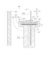
- FIG. 2 is a cross-sectional view of the current sensor taken along line 2-2 in FIG.
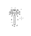
- FIG. 2 is the schematic which shows the relationship between the vector of magnetic flux, and a magnetic sensor when the center of an electric wire and the center of a magnetic sensor are substantially in agreement.
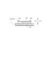
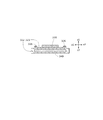
- FIG. 2 it is the schematic which shows the relationship between the vector of magnetic flux, and a magnetic sensor when the center of an electric wire and the center of a magnetic sensor have shifted
- FIG. 1 is a perspective view of a current sensor 100 of the present embodiment.
- FIG. 2 is a cross-sectional view of the current sensor 100 taken along a line 2-2 in FIG. 1 and parallel to the xz plane.
- the x direction, the y direction, and the z direction orthogonal to each other are defined.
- the x direction is expressed without distinguishing the x1 direction and the x2 direction that are opposite to each other.
- the y direction represents the y1 direction and the y2 direction that are opposite to each other without distinction.
- the z direction represents the z1 direction and the z2 direction that are opposite to each other without distinction.
- the current sensor 100 is a magnetic sensor that detects a magnetic field generated by a current flowing through the first electric wire 110, the fixing member 120, and the first electric wire 110 having a width in the z direction larger than the thickness in the x direction. 130, a magnetic field forming member 140 that includes a soft magnetic body and forms a magnetic field, and a second electric wire 180 (also referred to as an adjacent electric wire) having a width in the z direction larger than a thickness in the x direction.
- the fixing member 120 fixes the first electric wire 110, the magnetic sensor 130, and the magnetic field forming member 140.
- the second electric wire 180 is fixed to the first electric wire 110, the magnetic sensor 130, and the magnetic field forming member 140 by a fixing member (not shown).
- FIG. 13 is a schematic diagram showing the relationship between the magnetic flux vector generated by the current flowing through the second electric wire 180 and the magnetic sensor 130 and the first electric wire 110 in the case of the comparative example.
- magnetic flux lines are also formed around the second electric wire 180 in an elliptical shape.
- the magnetic field by the second electric wire 180 is substantially parallel to the z direction at a position facing the center in the z direction of the second electric wire 180 in the x direction.
- the magnetic field shaping member 140 stabilizes the magnetic flux vector in the vicinity of the magnetic sensor 130, and the magnetic sensor 130 and the magnetic field shaping member 140 fixed to each other are connected to the first first electric wire 110 and the second electric wire. Even when the position is slightly shifted from 180, the magnetic flux vector in the vicinity of the magnetic sensor 130 is unlikely to change. In particular, since the magnetic flux generated by the current flowing through the second electric wire 180 is close to the normal direction of the first outer surface 141 near the magnetic field forming member 140, the magnetic sensor 130 is shifted from the center of the second electric wire 180 in the z direction. Even if it exists, it is hard to receive the influence of the magnetic flux which the 2nd electric wire 180 generate
- the magnetic field forming member 140 is located between the first electric wire 110 and the magnetic sensor 130, the magnetic flux density near the magnetic sensor 130 is smaller than when the magnetic field forming member 140 is not provided.
- the magnetic sensor 130 can measure up to a large current.
- the first substrate 122 to which the magnetic field forming member 140 is fixed and the second substrate 123 to which the magnetic sensor 130 is fixed are prepared separately, so that the design of the first substrate 122 and the magnetic sensor 130 can be improved as compared with the case of fixing to one substrate. Since the first substrate 122 and the second substrate 123 are fixed by heat welding with a high degree of freedom, the magnetic field forming member 140 and the magnetic sensor 130 can be fixed with high positional accuracy.
- FIG. 8 is a partial cross-sectional view of the first modified example in the same cross section as FIG.
- the first substrate 222 and the second substrate shown in FIG. 8 respectively. 223, boss 226, magnetic sensor 230, and magnetic field forming member 240 are used.
- the magnetic sensor 130 is fixed to the z1 side of the second substrate 123, whereas in the first modification (FIG. 8), the magnetic sensor 230 is z2 of the second substrate 223. It is fixed on the side. Therefore, the boss 226 of the first modification (FIG. 8) is longer in the z direction than the boss 126 of the first embodiment (FIG. 2), and the first substrate 222 and the second substrate 223 of the first modification (FIG. 8). Is larger than the distance between the first substrate 122 and the second substrate 123 in the z direction in the first embodiment (FIG. 2). Other configurations are the same as those of the first embodiment.
- the relative positional relationship between the magnetic field forming member 240 and the magnetic sensor 230 shown in FIG. 8 and the first electric wire 110 and the second electric wire 180 shown in FIG. 2 is the same as that in the first embodiment. Therefore, the same effect as the first embodiment can be obtained.
- FIG. 9 is a partial cross-sectional view of the second modified example in the same cross section as FIG.
- a locking claw 326, a magnetic sensor 330, and a magnetic field forming member 340 are used.
- the second substrate 123 is fixed to the first substrate 122 by the boss 126, whereas in the second modification (FIG. 9), the second substrate 323 is the locking claw 326.
- the first substrate 322 is fixed. Since the surface on the z1 side of the first substrate 122 and the surface on the z2 side of the second substrate 323 are in close contact, the first substrate 122 and the second substrate 323 can be more firmly fixed. Other configurations are the same as those of the first embodiment.
- the major difference between the first embodiment (FIG. 2) and the second embodiment (FIG. 10) is the position of the magnetic field forming member 440 and the magnetic sensor 430.
- the difference between the first embodiment (FIG. 2) and the second embodiment (FIG. 10) will be mainly described.
- a magnetic field forming member 440 is embedded and fixed inside the first substrate 422 of the second embodiment (FIG. 10).
- a magnetic sensor 430 is fixed to the surface on the z1 side of the second substrate 423 of the second embodiment (FIG. 10).
- the first substrate 422 of the second embodiment (FIG. 10) is located on the z1 side of the second substrate 423.
- the magnetic sensor 430 is located between the first electric wire 410 and the magnetic field forming member 440 in the z direction.
- Both the magnetic sensor 430 and the magnetic field forming member 440 are disposed at positions overlapping the second electric wire 480 in the x direction. That is, the magnetic sensor 430 and the magnetic field shaping member 440 are located on the z2 side with respect to the z1 side end of the second electric wire 480.
- the magnetic field forming member 440 Since the magnetic field forming member 440 has a strong force for forming a magnetic field, even if the magnetic sensor 430 and the magnetic field forming member 440 are slightly displaced in the z direction with respect to the second electric wire 480, the magnetic force generated by the second electric wire 480 is increased. The magnetic field near the sensor 430 does not change significantly. In the vicinity of the magnetic field forming member 440, the magnetic field generated by the second electric wire 480 is fixed substantially parallel to the z direction. Therefore, even if the magnetic sensor 430 is disposed at a position shifted in the z direction from the center in the z direction of the second electric wire 480, the magnetic sensor 430 is hardly affected by the second electric wire 480 and moves slightly in the z direction. However, the degree of influence on the measured value is difficult to change.
- the magnetic sensor 430 since the magnetic sensor 430 is located between the first electric wire 410 and the magnetic field shaping member 440, the magnetic field shaping member 440 is arranged at the same position, and the magnetic field shaping member 440 is replaced with the first electric wire 410. And the magnetic sensor 430 can be reduced in size. Further, since the magnetic field is not easily blocked by the magnetic field shaping member 440, the signal-to-noise ratio can be reduced, and the magnetic sensor 430 can easily detect a small change in the magnetic field.
- the distal second substrate 523-2, the distal boss 526-2, the distal magnetic field shaping member 540-2, the distal first outer surface 541-2, and the distal second outer surface 542 of the third embodiment (FIG. 11) -2 corresponds to the second substrate 423, the boss 426, the magnetic field forming member 440, the first outer surface 441, and the second outer surface 442 of the second embodiment (FIG. 10), respectively.
- the proximal magnetic field shaping member 540-1 and the distal magnetic field shaping member 540-2 may be referred to as the magnetic field shaping member 540 without being distinguished from each other.
- FIG. 11 has the structure which combined 1st Embodiment (FIG. 2) and 2nd Embodiment (FIG. 10).
- the current sensor 500 includes two magnetic field shaping members 540, and the magnetic sensor 530 is located between one magnetic field shaping member 540 and another magnetic field shaping member 540. This is different from the first embodiment (FIG. 2) and the second embodiment (FIG. 10).
- the current sensor 500 according to the third embodiment (FIG. 11) will be described mainly with respect to differences between the current sensor 100 according to the first embodiment (FIG. 2) and the current sensor 400 according to the second embodiment (FIG. 10). To do.
- the magnetic field vector around the magnetic field shaping member 540 of the third embodiment is the same as the magnetic field shaping member 540 in the x direction. Even if it moves slightly, it does not change greatly compared to the case where the magnetic field shaping member 540 is not provided. Since the magnetic sensor 430 is fixed in the formed magnetic field between the two magnetic field forming members 540, even if the magnetic sensor 430 moves slightly in the x direction, the magnetic flux vector near the magnetic sensor 530 changes greatly. Absent.
- the magnetic field forming member 540 is located between the first electric wire 510 and the magnetic sensor 530, the magnetic flux density near the magnetic sensor 530 is smaller than when the magnetic field forming member 540 is not provided. Since the magnetic sensor 530 can measure up to a large current, and the magnetic field forming members 540 are disposed on both sides of the magnetic sensor 530, the magnetic sensor with respect to the positional deviation compared to the case where the number of the magnetic field forming members 540 is one. The change in the magnetic flux vector near 530 is small.
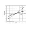
- FIG. 12 is a graph showing the relationship between the positional deviation (horizontal axis) and the adjacent influence variation (vertical axis) in the experiment.
- the positional deviation represents the deviation between the center of the magnetic sensor 130 and the center of the first electric wire 110 in the z direction in mm.
- the adjacent influence variation represents the ratio of the change amount of the measurement value to the measurement value when the positional deviation is 0 mm.
- the positional shift is positive in the z1 direction and negative in the z1 direction.
- the sign of the adjacent influence variation represents the difference in the direction of the magnetic flux vector.
- a graph 181 represents the case of the second embodiment shown in FIG.
- the width in the z direction of the narrow region 412 shown in FIG. 10 is 5 mm
- the width in the z direction of the second electric wire 480 is 12.5 mm
- the distance in the z direction between the center of the magnetic sensor 430 and the first electric wire 410 in the z direction is 3.
- the distance in the z direction between the first outer surface 441 of the magnetic field shaping member 440 and the center of the magnetic sensor 430 in the z direction was 3 mm
- the thickness in the z direction of the magnetic field shaping member 440 was 1 mm.
- Graph 182 represents the case of the third embodiment shown in FIG.
- the width in the z direction of the narrow region 512 shown in FIG. 11 is 5 mm
- the width in the z direction of the second electric wire 580 is 12.5 mm
- the distance in the z direction between the center of the magnetic sensor 530 and the first electric wire 510 in the z direction is 3.
- the spacing in the z direction between the proximal first outer surface 441-1 of the proximal magnetic field shaping member 540-1 and the center of the magnetic sensor 530 in the z direction is 1.5 mm
- the z of the proximal magnetic field shaping member 540-1 The thickness in the direction is 1 mm
- the distance in the z direction between the distal first outer surface 441-2 of the distal magnetic field shaping member 540-2 and the center of the magnetic sensor 530 in the z direction is 3 mm
- the distal magnetic field shaping member 540-2 The thickness in the z direction was 1 mm.
- Graph 183 represents a comparative example in which the magnetic field forming member 440 is not used under the same conditions as in the second embodiment shown in FIG.
- the absolute value of the adjacent influence variation increases as the positional deviation in the z direction increases (that is, the deviation from the measured value when the positional deviation is 0 mm increases).
- the change in the adjacent influence variation is smaller than that in the comparative example (graph 183). That is, in the second embodiment and the third embodiment, the influence on the measurement value due to the displacement in the z direction is smaller than in the comparative example.
- the present invention can be applied to various current sensors.
Landscapes
- Physics & Mathematics (AREA)
- General Physics & Mathematics (AREA)
- Measuring Instrument Details And Bridges, And Automatic Balancing Devices (AREA)
Abstract
Selon l'invention, un capteur magnétique (130) est disposé en une position de superposition avec un second fil électrique (180) dans une direction x, un élément de moulage de champ magnétique (140) consiste en un élément plat s'élargissant de manière sensiblement parallèle à un plan perpendiculaire à une direction z, et contient une face externe s'opposant au capteur magnétique (130). Cette face externe et la direction d'un axe de sensibilité du capteur magnétique (130) sont sensiblement parallèles dans la direction x. L'élément fixe (120) fixe le capteur magnétique (130) et l'élément de moulage de champ magnétique (140) par rapprochement d'un même côté de la direction z par rapport au premier fil électrique (110), et fixe au moins une partie du premier fil électrique (110), au moins une partie du capteur magnétique (130) et au moins une partie de l'élément de moulage de champ magnétique (140) par éloignement vers des positions se superposant dans la direction z.
Applications Claiming Priority (2)
| Application Number | Priority Date | Filing Date | Title |
|---|---|---|---|
| JP2016-140929 | 2016-07-15 | ||
| JP2016140929 | 2016-07-15 |
Publications (1)
| Publication Number | Publication Date |
|---|---|
| WO2018012034A1 true WO2018012034A1 (fr) | 2018-01-18 |
Family
ID=60951736
Family Applications (1)
| Application Number | Title | Priority Date | Filing Date |
|---|---|---|---|
| PCT/JP2017/009967 Ceased WO2018012034A1 (fr) | 2016-07-15 | 2017-03-13 | Capteur de courant |
Country Status (1)
| Country | Link |
|---|---|
| WO (1) | WO2018012034A1 (fr) |
Cited By (1)
| Publication number | Priority date | Publication date | Assignee | Title |
|---|---|---|---|---|
| WO2019117174A1 (fr) * | 2017-12-13 | 2019-06-20 | アルプスアルパイン株式会社 | Capteur de courant |
Citations (9)
| Publication number | Priority date | Publication date | Assignee | Title |
|---|---|---|---|---|
| US6734660B1 (en) * | 2002-02-07 | 2004-05-11 | Lockheed Martin Corporation | Current sensor arrangement with test current generator |
| JP2015111080A (ja) * | 2013-12-06 | 2015-06-18 | トヨタ自動車株式会社 | バスバモジュール |
| JP2015111079A (ja) * | 2013-12-06 | 2015-06-18 | トヨタ自動車株式会社 | バスバモジュール |
| JP2015152418A (ja) * | 2014-02-14 | 2015-08-24 | トヨタ自動車株式会社 | 電流センサ |
| JP2016038203A (ja) * | 2014-08-05 | 2016-03-22 | トヨタ自動車株式会社 | 電流センサ |
| WO2016098511A1 (fr) * | 2014-12-15 | 2016-06-23 | 株式会社村田製作所 | Capteur de courant |
| JP2016125907A (ja) * | 2015-01-05 | 2016-07-11 | トヨタ自動車株式会社 | 電流センサ |
| JP2016173334A (ja) * | 2015-03-18 | 2016-09-29 | トヨタ自動車株式会社 | 電流センサ |
| JP2016200436A (ja) * | 2015-04-08 | 2016-12-01 | トヨタ自動車株式会社 | 電流センサ |
-
2017
- 2017-03-13 WO PCT/JP2017/009967 patent/WO2018012034A1/fr not_active Ceased
Patent Citations (9)
| Publication number | Priority date | Publication date | Assignee | Title |
|---|---|---|---|---|
| US6734660B1 (en) * | 2002-02-07 | 2004-05-11 | Lockheed Martin Corporation | Current sensor arrangement with test current generator |
| JP2015111080A (ja) * | 2013-12-06 | 2015-06-18 | トヨタ自動車株式会社 | バスバモジュール |
| JP2015111079A (ja) * | 2013-12-06 | 2015-06-18 | トヨタ自動車株式会社 | バスバモジュール |
| JP2015152418A (ja) * | 2014-02-14 | 2015-08-24 | トヨタ自動車株式会社 | 電流センサ |
| JP2016038203A (ja) * | 2014-08-05 | 2016-03-22 | トヨタ自動車株式会社 | 電流センサ |
| WO2016098511A1 (fr) * | 2014-12-15 | 2016-06-23 | 株式会社村田製作所 | Capteur de courant |
| JP2016125907A (ja) * | 2015-01-05 | 2016-07-11 | トヨタ自動車株式会社 | 電流センサ |
| JP2016173334A (ja) * | 2015-03-18 | 2016-09-29 | トヨタ自動車株式会社 | 電流センサ |
| JP2016200436A (ja) * | 2015-04-08 | 2016-12-01 | トヨタ自動車株式会社 | 電流センサ |
Cited By (3)
| Publication number | Priority date | Publication date | Assignee | Title |
|---|---|---|---|---|
| WO2019117174A1 (fr) * | 2017-12-13 | 2019-06-20 | アルプスアルパイン株式会社 | Capteur de courant |
| JPWO2019117174A1 (ja) * | 2017-12-13 | 2020-10-01 | アルプスアルパイン株式会社 | 電流センサ |
| US11287451B2 (en) | 2017-12-13 | 2022-03-29 | Alps Alpine Co., Ltd. | Current sensor |
Similar Documents
| Publication | Publication Date | Title |
|---|---|---|
| JP6403086B2 (ja) | 電流検出構造 | |
| JP6119296B2 (ja) | 電流センサ | |
| CN205280791U (zh) | 电流传感器 | |
| JP2015137892A (ja) | 電流検出構造 | |
| JP5817508B2 (ja) | 電流検出装置 | |
| JP6327874B2 (ja) | 誘導型位置測定装置 | |
| JP2016125907A (ja) | 電流センサ | |
| KR20170124406A (ko) | 전류 센서 | |
| JP5092872B2 (ja) | 面状温度検出センサ | |
| JP2015148470A (ja) | 電流検出構造 | |
| JP6598040B2 (ja) | 電流検出構造 | |
| JP2015141121A (ja) | 磁気センサ | |
| JP3191252U (ja) | 電流センサ | |
| JP6572744B2 (ja) | 電流センサ | |
| JP6654241B2 (ja) | 電流センサ | |
| JP6560637B2 (ja) | 電流センサ、シールド、および製造方法 | |
| US11215645B2 (en) | Current sensor | |
| JP2016161529A (ja) | 電流センサ | |
| JP2015132514A (ja) | 電流検出構造 | |
| JP6626199B2 (ja) | 電流センサ | |
| WO2013108767A1 (fr) | Dispositif de détection de courant électrique | |
| JP6144597B2 (ja) | 電流センサ | |
| JP2015148469A (ja) | 電流検出構造 | |
| JP2016125991A (ja) | 電流測定装置 | |
| JP5952652B2 (ja) | 電流センサ |
Legal Events
| Date | Code | Title | Description |
|---|---|---|---|
| 121 | Ep: the epo has been informed by wipo that ep was designated in this application |
Ref document number: 17827168 Country of ref document: EP Kind code of ref document: A1 |
|
| NENP | Non-entry into the national phase |
Ref country code: DE |
|
| NENP | Non-entry into the national phase |
Ref country code: JP |
|
| 122 | Ep: pct application non-entry in european phase |
Ref document number: 17827168 Country of ref document: EP Kind code of ref document: A1 |