WO2018016181A1 - Élément de réception de lumière, procédé de fabrication d'élément de réception de lumière, appareil d'imagerie et dispositif électronique - Google Patents
Élément de réception de lumière, procédé de fabrication d'élément de réception de lumière, appareil d'imagerie et dispositif électronique Download PDFInfo
- Publication number
- WO2018016181A1 WO2018016181A1 PCT/JP2017/019731 JP2017019731W WO2018016181A1 WO 2018016181 A1 WO2018016181 A1 WO 2018016181A1 JP 2017019731 W JP2017019731 W JP 2017019731W WO 2018016181 A1 WO2018016181 A1 WO 2018016181A1
- Authority
- WO
- WIPO (PCT)
- Prior art keywords
- layer
- light
- receiving element
- photoelectric conversion
- light receiving
- Prior art date
- Legal status (The legal status is an assumption and is not a legal conclusion. Google has not performed a legal analysis and makes no representation as to the accuracy of the status listed.)
- Ceased
Links
Images














Classifications
-
- H—ELECTRICITY
- H10—SEMICONDUCTOR DEVICES; ELECTRIC SOLID-STATE DEVICES NOT OTHERWISE PROVIDED FOR
- H10F—INORGANIC SEMICONDUCTOR DEVICES SENSITIVE TO INFRARED RADIATION, LIGHT, ELECTROMAGNETIC RADIATION OF SHORTER WAVELENGTH OR CORPUSCULAR RADIATION
- H10F39/00—Integrated devices, or assemblies of multiple devices, comprising at least one element covered by group H10F30/00, e.g. radiation detectors comprising photodiode arrays
- H10F39/80—Constructional details of image sensors
- H10F39/813—Electronic components shared by multiple pixels, e.g. one amplifier shared by two pixels
-
- H—ELECTRICITY
- H10—SEMICONDUCTOR DEVICES; ELECTRIC SOLID-STATE DEVICES NOT OTHERWISE PROVIDED FOR
- H10F—INORGANIC SEMICONDUCTOR DEVICES SENSITIVE TO INFRARED RADIATION, LIGHT, ELECTROMAGNETIC RADIATION OF SHORTER WAVELENGTH OR CORPUSCULAR RADIATION
- H10F39/00—Integrated devices, or assemblies of multiple devices, comprising at least one element covered by group H10F30/00, e.g. radiation detectors comprising photodiode arrays
- H10F39/80—Constructional details of image sensors
- H10F39/805—Coatings
- H10F39/8057—Optical shielding
-
- H—ELECTRICITY
- H10—SEMICONDUCTOR DEVICES; ELECTRIC SOLID-STATE DEVICES NOT OTHERWISE PROVIDED FOR
- H10F—INORGANIC SEMICONDUCTOR DEVICES SENSITIVE TO INFRARED RADIATION, LIGHT, ELECTROMAGNETIC RADIATION OF SHORTER WAVELENGTH OR CORPUSCULAR RADIATION
- H10F39/00—Integrated devices, or assemblies of multiple devices, comprising at least one element covered by group H10F30/00, e.g. radiation detectors comprising photodiode arrays
- H10F39/011—Manufacture or treatment of image sensors covered by group H10F39/12
- H10F39/014—Manufacture or treatment of image sensors covered by group H10F39/12 of CMOS image sensors
-
- H—ELECTRICITY
- H10—SEMICONDUCTOR DEVICES; ELECTRIC SOLID-STATE DEVICES NOT OTHERWISE PROVIDED FOR
- H10F—INORGANIC SEMICONDUCTOR DEVICES SENSITIVE TO INFRARED RADIATION, LIGHT, ELECTROMAGNETIC RADIATION OF SHORTER WAVELENGTH OR CORPUSCULAR RADIATION
- H10F39/00—Integrated devices, or assemblies of multiple devices, comprising at least one element covered by group H10F30/00, e.g. radiation detectors comprising photodiode arrays
- H10F39/011—Manufacture or treatment of image sensors covered by group H10F39/12
- H10F39/024—Manufacture or treatment of image sensors covered by group H10F39/12 of coatings or optical elements
-
- H—ELECTRICITY
- H10—SEMICONDUCTOR DEVICES; ELECTRIC SOLID-STATE DEVICES NOT OTHERWISE PROVIDED FOR
- H10F—INORGANIC SEMICONDUCTOR DEVICES SENSITIVE TO INFRARED RADIATION, LIGHT, ELECTROMAGNETIC RADIATION OF SHORTER WAVELENGTH OR CORPUSCULAR RADIATION
- H10F39/00—Integrated devices, or assemblies of multiple devices, comprising at least one element covered by group H10F30/00, e.g. radiation detectors comprising photodiode arrays
- H10F39/10—Integrated devices
- H10F39/12—Image sensors
-
- H—ELECTRICITY
- H10—SEMICONDUCTOR DEVICES; ELECTRIC SOLID-STATE DEVICES NOT OTHERWISE PROVIDED FOR
- H10F—INORGANIC SEMICONDUCTOR DEVICES SENSITIVE TO INFRARED RADIATION, LIGHT, ELECTROMAGNETIC RADIATION OF SHORTER WAVELENGTH OR CORPUSCULAR RADIATION
- H10F39/00—Integrated devices, or assemblies of multiple devices, comprising at least one element covered by group H10F30/00, e.g. radiation detectors comprising photodiode arrays
- H10F39/10—Integrated devices
- H10F39/12—Image sensors
- H10F39/18—Complementary metal-oxide-semiconductor [CMOS] image sensors; Photodiode array image sensors
- H10F39/184—Infrared image sensors
-
- H—ELECTRICITY
- H10—SEMICONDUCTOR DEVICES; ELECTRIC SOLID-STATE DEVICES NOT OTHERWISE PROVIDED FOR
- H10F—INORGANIC SEMICONDUCTOR DEVICES SENSITIVE TO INFRARED RADIATION, LIGHT, ELECTROMAGNETIC RADIATION OF SHORTER WAVELENGTH OR CORPUSCULAR RADIATION
- H10F39/00—Integrated devices, or assemblies of multiple devices, comprising at least one element covered by group H10F30/00, e.g. radiation detectors comprising photodiode arrays
- H10F39/80—Constructional details of image sensors
- H10F39/805—Coatings
- H10F39/8053—Colour filters
-
- H—ELECTRICITY
- H10—SEMICONDUCTOR DEVICES; ELECTRIC SOLID-STATE DEVICES NOT OTHERWISE PROVIDED FOR
- H10F—INORGANIC SEMICONDUCTOR DEVICES SENSITIVE TO INFRARED RADIATION, LIGHT, ELECTROMAGNETIC RADIATION OF SHORTER WAVELENGTH OR CORPUSCULAR RADIATION
- H10F39/00—Integrated devices, or assemblies of multiple devices, comprising at least one element covered by group H10F30/00, e.g. radiation detectors comprising photodiode arrays
- H10F39/80—Constructional details of image sensors
- H10F39/806—Optical elements or arrangements associated with the image sensors
- H10F39/8063—Microlenses
-
- H—ELECTRICITY
- H10—SEMICONDUCTOR DEVICES; ELECTRIC SOLID-STATE DEVICES NOT OTHERWISE PROVIDED FOR
- H10F—INORGANIC SEMICONDUCTOR DEVICES SENSITIVE TO INFRARED RADIATION, LIGHT, ELECTROMAGNETIC RADIATION OF SHORTER WAVELENGTH OR CORPUSCULAR RADIATION
- H10F39/00—Integrated devices, or assemblies of multiple devices, comprising at least one element covered by group H10F30/00, e.g. radiation detectors comprising photodiode arrays
- H10F39/80—Constructional details of image sensors
- H10F39/807—Pixel isolation structures
-
- H—ELECTRICITY
- H10—SEMICONDUCTOR DEVICES; ELECTRIC SOLID-STATE DEVICES NOT OTHERWISE PROVIDED FOR
- H10F—INORGANIC SEMICONDUCTOR DEVICES SENSITIVE TO INFRARED RADIATION, LIGHT, ELECTROMAGNETIC RADIATION OF SHORTER WAVELENGTH OR CORPUSCULAR RADIATION
- H10F39/00—Integrated devices, or assemblies of multiple devices, comprising at least one element covered by group H10F30/00, e.g. radiation detectors comprising photodiode arrays
- H10F39/80—Constructional details of image sensors
- H10F39/811—Interconnections
-
- H—ELECTRICITY
- H04—ELECTRIC COMMUNICATION TECHNIQUE
- H04N—PICTORIAL COMMUNICATION, e.g. TELEVISION
- H04N25/00—Circuitry of solid-state image sensors [SSIS]; Control thereof
- H04N25/70—SSIS architectures; Circuits associated therewith
- H04N25/76—Addressed sensors, e.g. MOS or CMOS sensors
- H04N25/78—Readout circuits for addressed sensors, e.g. output amplifiers or A/D converters
Definitions
- the present disclosure relates to a light receiving element used for, for example, an infrared sensor, a manufacturing method thereof, an imaging apparatus, and an electronic apparatus.
- CMOS Complementary Metal Oxide ⁇ ⁇ Semiconductor
- Patent Document 1 discloses a structure in which a light shielding layer is disposed around each pixel on a transparent electrode layer provided on a compound semiconductor layer.
- the pixel size has been reduced, and further generation of color mixing is required to be suppressed.
- a light receiving element includes a plurality of pixels, a photoelectric conversion layer common to the plurality of pixels, a first electrode layer provided on a light incident surface side of the photoelectric conversion layer, and a first A light-shielding portion embedded between a plurality of adjacent pixels of the electrode layer.
- a method for manufacturing a light receiving element includes: forming a common photoelectric conversion layer for a plurality of pixels; and forming a first electrode layer on a light incident surface side of the photoelectric conversion layer; And forming a light shielding portion embedded between a plurality of adjacent pixels of the first electrode layer.
- the light shielding portion is embedded between the adjacent pixels of the first electrode layer provided on the light incident surface side, thereby obliquely incident. It becomes possible to reduce the incidence of light on adjacent pixels.
- An imaging device includes a plurality of pixels, a photoelectric conversion layer common to the plurality of pixels, a first electrode layer provided on a light incident surface side of the photoelectric conversion layer, and a first A light-shielding portion embedded between a plurality of adjacent pixels of the electrode layer.
- An electronic apparatus includes the imaging device according to the embodiment of the present disclosure.
- the method for manufacturing the light receiving element of one embodiment, the imaging device of one embodiment, and the electronic apparatus of one embodiment the first light provided on the light incident surface side of the photoelectric conversion layer Since the light shielding portion is embedded between adjacent pixels of one electrode layer, the incidence of oblique incident light on the adjacent pixels is reduced. Therefore, it is possible to suppress the occurrence of color mixing.
- FIG. 5C It is sectional drawing showing the process of following FIG. 5C. It is sectional drawing showing the process of following FIG. 5D. It is a cross-sectional schematic diagram explaining an example of generation
- Embodiment an example of a light receiving element in which a light shielding portion is embedded between transparent electrodes provided for each pixel
- Action / Effect Modification 3 Application example Application example 1 (example of imaging device)
- Application Example 2 Example of electronic equipment
- Application example 3 example of in-vivo information acquisition system
- Application example 4 (example of mobile control system)
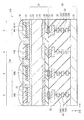
- FIG. 1 illustrates a cross-sectional configuration of a light receiving element (light receiving element 10A) according to an embodiment of the present disclosure.
- the light receiving element 10A includes, for example, a plurality of light receiving unit areas (referred to as pixels P) arranged two-dimensionally. It has a photoelectric conversion function with respect to the wavelength.
- the light receiving element 10A is applied to, for example, an infrared sensor.
- the light receiving element 10A includes, for example, a photoelectric conversion layer 22 and a cap layer 23 (second semiconductor layer) on one surface (surface opposite to the light incident surface S1 (back surface S2)) of the substrate 21 (first semiconductor layer). Are stacked in this order.
- a protective layer 24 is further provided on the cap layer 23. Inside the protective layer 24, a contact electrode 25 (second electrode) that is electrically connected to a selective region (first conductivity type region 23A) of the cap layer 23 is provided.
- the substrate 21 to the protective layer 24 having the contact electrode 25 are referred to as a semiconductor substrate 20.
- a plurality of transparent electrodes (first electrode layers) 41 formed separately for each pixel P are provided on the light incident surface S1 side of the substrate 21, and a light shielding portion 42 is provided between the plurality of transparent electrodes 41. Buried.
- a protective layer 43 is provided on the transparent electrode 41 and the light shielding portion 42, and a color filter 44 and an on-chip lens (condensing lens) 45 are further stacked in this order via the protective layer 43. Further, a multilayer wiring substrate 30 having a readout circuit is bonded to the back surface S2 side of the semiconductor substrate 20.
- the configuration of each unit will be described.
- the substrate 21 is made of, for example, an n-type or i-type (intrinsic semiconductor) III-V group semiconductor.
- the photoelectric conversion layer 22 is formed in contact with the substrate 21 on the back surface S 2 side, but another layer may be interposed between the substrate 21 and the photoelectric conversion layer 22.
- the material of the layer interposed between the substrate 21 and the photoelectric conversion layer 22 include compound semiconductors such as InAlAs, Ge, Si, GaAs, InP, InGaAsP, and AlGaAs. It is desirable to select one that lattice-matches with.
- the photoelectric conversion layer 22 includes, for example, a compound semiconductor that absorbs wavelengths in the infrared region (hereinafter referred to as infrared rays) and generates charges (electrons and holes).
- the photoelectric conversion layer 22 is continuously provided on the substrate 21 as a common layer for the plurality of pixels P (or the plurality of contact electrodes 25).
- the compound semiconductor used for the photoelectric conversion layer 22 is, for example, a group III-V semiconductor, and examples thereof include In x Ga (1-x) As (x: 0 ⁇ x ⁇ 1). However, in order to obtain more sensitivity in the infrared region, it is desirable that x ⁇ 0.4.
- the photoelectric conversion layer 22 has a pn junction or a pin junction by stacking a first conductivity type region 22A described later and a region (second conductivity type region 22B) other than the first conductivity type region 22A.
- the second conductivity type region 22B formed in the photoelectric conversion layer 22 is a region containing, for example, an n-type impurity. Examples of the n-type impurity include silicon (Si). However, the second conductivity type region 22B may be made of an intrinsic semiconductor (may be an i-type semiconductor region).
- the cap layer 23 is provided between the photoelectric conversion layer 22 and the protective layer 24 on which the contact electrode 25 is provided. Although the details will be described later, the cap layer 23 preferably has a role of electrically separating pixels or suppressing generation of dark current.
- the cap layer 23 is preferably configured to include a compound semiconductor having a larger band gap than the photoelectric conversion layer 22. Examples of large compound semiconductor bandgap than In 0.53 Ga 0.47 As (band gap 0.74 eV), InP (band gap 1.34 eV) or InAlAs and the like, for example. Note that a layer made of any one of InAlAs, Ge, Si, GaAs, InP, and the like may be further interposed between the cap layer 23 and the photoelectric conversion layer 22.
- a first conductivity type region 23A is formed in a selective region.
- the first conductivity type region 23A is formed for each pixel P.
- a plurality of first conductivity type regions 23 ⁇ / b> A are formed discretely from each other in the cap layer 23.
- the first conductivity type region 23A is, for example, a region containing a p-type impurity (p-type impurity region).
- An example of the p-type impurity is zinc (Zn).
- the first conductivity type region 23A extends from the surface of the cap layer 23 facing the multilayer wiring board 30 to a predetermined depth position, for example, a part of the first conductivity type region 23A extends into the photoelectric conversion layer 22 as shown in FIG. is doing.
- the first conductivity type region 23 ⁇ / b> A formed in the cap layer 23 is the first conductivity type region 22 ⁇ / b> A in the photoelectric conversion layer 22.
- a second conductivity type region 23B is formed adjacent to the first conductivity type region 23A.
- the p-type impurity region forming the first conductivity type region 23 ⁇ / b> A does not necessarily need to extend to the photoelectric conversion layer 22.
- the boundary of the p-type impurity region may coincide with the interface between the cap layer 23 and the photoelectric conversion layer 22, or may be formed in the layer of the cap layer 23.
- the first conductivity type region 23A and the second conductivity type region 23B are formed adjacent to each other in the lateral direction at the boundary between the first conductivity type region 23A and the second conductivity type region 23B. As a result, a pn junction interface is formed. Thereby, adjacent pixels P are electrically separated.
- the protective layer 24 is formed on the cap layer 23 and is formed using an inorganic insulating material.
- the inorganic insulating material include silicon nitride (SiN), aluminum oxide (Al 2 O 3 ), silicon oxide (SiO 2 ), and hafnium oxide (HfO 2 ).
- the protective layer 24 includes at least one of these.
- the protective layer 24 has an opening H ⁇ b> 1 (see FIG. 5B) at a position facing the first conductivity type region 23 ⁇ / b> A of the cap layer 23. That is, the first conductivity type region 23A and the opening H1 are provided for each pixel P.
- the contact electrode 25 is an electrode to which a voltage for reading out charges (for example, holes) generated in the photoelectric conversion layer 22 is supplied, and is formed for each pixel P.
- Examples of the constituent material of the contact electrode 25 include titanium (Ti), tungsten (W), titanium nitride (TiN), platinum (Pt), gold (Au), germanium (Ge), palladium (Pd), and zinc (Zn). ), Nickel (Ni) and aluminum (Al), or an alloy containing at least one of them.
- the contact electrode 25 may be a single layer film made of the above-described constituent materials, or may be formed as a laminated film in which two or more kinds are combined, for example.
- the contact electrode 25 embeds the opening H1 and is electrically connected via the first conductivity type region 22A and the first conductivity type region 23A of the photoelectric conversion layer 22.
- the contact electrode 25 fills the opening H1, and is in direct contact with the surface of the first conductivity type region 23A.
- the contact electrode 25 is provided for each pixel P, one contact electrode 25 may be arranged for one pixel P as in the present embodiment, or one pixel P A plurality of contact electrodes 25 may be arranged. When a plurality of contact electrodes 25 are arranged in one pixel P, some of them may include electrodes (dummy electrodes) that do not actually contribute to charge extraction.
- connection layer 26 that protrudes (protrudes) in the X-axis direction from the side surface of the opening H1 is provided. That is, the connection layer 26 is formed in a bowl shape on the contact electrode 25. The connection layer 26 is for electrically connecting the contact electrode 25 and the readout electrode 36.
- the multilayer wiring board 30 is provided with an interlayer insulating layer 32 on a support substrate 31 made of, for example, Si, and a readout circuit for reading signals from each pixel P is formed between the interlayer insulating layers 32. ing.
- This readout circuit is composed of, for example, a pixel circuit 35 and a wiring layer 34 having various wirings 34A, 34B, and 34C.
- the pixel circuit 35 and the various wirings 34A, 34B, and 34C are electrically connected by through electrodes 33A, 33B, 33C, and 33D, respectively.
- a readout electrode 36 is provided on the pixel circuit 35 and is electrically connected to the pixel circuit 35.
- connection layer 37 formed in a bowl shape is formed on the readout electrode 36.
- the read electrode 36 is electrically connected to the contact electrode 25 by bonding the connection layer 37 and the connection layer 26 on the semiconductor substrate 20 side. Thereby, charges (for example, holes) generated in the photoelectric conversion layer 22 can be read out for each pixel P.
- the transparent electrode 41 is individually formed for each pixel P on the light incident surface S1 of the substrate 21.
- the transparent electrode 41 is electrically connected to the substrate 21.
- the light receiving element 10 ⁇ / b> A of the present embodiment for example, when holes are read out as signal charges through the contact electrode 25 among the charges generated in the photoelectric conversion layer 22, for example, electrons are discharged through the transparent electrode 41. it can.
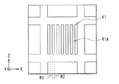
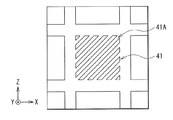
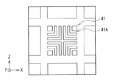
- the planar shape of the transparent electrode 41 provided for each pixel P is not particularly limited.
- the planar shape of the transparent electrode 41 may be a rectangular shape as shown in FIG. 2A, for example, or may be a shape obtained by rotating the transparent electrode 41 shown in FIG. 2A by 45 degrees as shown in FIG. 2B. .
- the transparent electrode 41 does not need to be a solid film formed uniformly for each pixel P.
- a plurality of slits 41A may be formed. .
- the transparent electrode 41 can be used as an electrode for a polarization sensor.
- the width (pitch; W1) of each slit 41A and the electrode width (line width; W2) between the slits 41A when used as an electrode for a polarization sensor are, for example, a slit width W1 of 0.2 ⁇ m and an electrode width W2.
- 0.5 ⁇ m can be mentioned.
- 2C to 2G show an example in which the transparent electrode 41 is separated into a plurality of sections by the slit 41A, but the present invention is not limited to this.
- the slit 41 ⁇ / b> A may be formed in the plane so as to leave the outer edge portion of the transparent electrode 41.
- the constituent material of the transparent electrode 41 examples include titanium (Ti), tungsten (W), titanium nitride (TiN), platinum (Pt), gold (Au), germanium (Ge), nickel (Ni), and aluminum (Al). Of any of these, or an alloy containing at least one of them.
- indium titanium oxide (ITO) has high transparency in the infrared region, and is desirable as a constituent material of the transparent electrode 41.
- the transparent electrode 41 is made of indium tin oxide (ITO), tin (Sn), tin oxide (SnO 2 ), IWO, indium-zinc composite oxide (IZO), aluminum oxide doped with zinc ( AZO), zinc-doped gallium oxide (GZO), magnesium and zinc-doped aluminum oxide (AlMgZnO), indium-gallium composite oxide (IGO), In-GaZnO 4 (IGZO), fluorine-doped indium oxide ( IFO), tin oxide doped with antimony (ATO), tin oxide doped with fluorine (FTO), zinc oxide (ZnO), ZnO doped with boron, and InSnZnO.
- ITO indium tin oxide
- Sn tin
- SnO 2 tin oxide
- IWO indium-zinc composite oxide
- IZO indium-zinc composite oxide
- AZO zinc-doped gallium oxide
- AlMgZnO aluminum
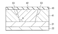
- the light-shielding portion 42 is embedded between the transparent electrodes 41 provided for each pixel P, that is, between adjacent pixels P, and prevents incident light from entering obliquely adjacent pixels.
- the side surface S3 of the light shielding portion 42 is shown to be perpendicular to the semiconductor substrate 20 in FIG. 1, it is not limited thereto.
- the semiconductor substrate 20 (substrate 21) and the side surface S3 may have a forward tapered shape with an acute angle ⁇ , or as shown in FIG. 4B, the semiconductor substrate 20 (substrate 21).
- the side surface S3 may have an inverted taper shape with an obtuse angle ⁇ .
- the side surface S3 of the light shielding portion 42 may be a curved surface.
- the side surface 3 may be convex or concave.
- the forward tapered light-shielding portion 42 is preferable because light can be easily taken into the photoelectric conversion layer 22 and light utilization efficiency can be improved.
- the width W3 in the X-axis direction of the light shielding part 42 only needs to ensure light shielding properties. Moreover, it is good also as a different width
- Examples of the constituent material of the light shielding portion 42 include titanium (Ti), tungsten (W), carbon (C), chromium oxide (Cr 2 O 3 ), an alloy of samarium (Sm) and silver (Ag), or an organic material. Is mentioned.
- the light shielding portion 42 is configured as a single layer film or a laminated film made of these materials. Specific examples of the laminated film include a metal laminated film such as Ti / W.
- the light shielding part 42 may be formed using a material containing, for example, Ti, Pt, and Au in addition to the above materials.
- the protective layer 43 is for flattening the surfaces of the transparent electrode 41 and the light shielding part 42, and is formed by using an inorganic insulating material, for example, like the protective layer 24.
- the inorganic insulating material include silicon nitride (SiN x ), silicon oxide (SiO x ), aluminum oxide (Al 2 O 3 ), and hafnium oxide (HfO 2 ).
- the protective layer 43 includes at least one of these.
- the color filter 44 is provided on the protective layer 43, and for example, any one of a red filter (44R), a green filter (44G), a blue filter (44B), and an IR filter (44I) is arranged for each pixel P. These color filters 44 are provided in a regular color arrangement (for example, a Bayer arrangement). By providing such a color filter 44, the light receiving element 10A can obtain light receiving data having a wavelength corresponding to the color arrangement.
- the on-chip lens 45 has a function of condensing light toward the photoelectric conversion layer 22.
- the lens material include an organic material and a silicon oxide film (SiO 2 ).
- the light receiving element 10A can be manufactured, for example, as follows. 5A to 5E show the manufacturing process of the light receiving element 10A in the order of steps.
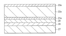
- the absorption layer 22a made of InGaAs to be the layer 22 and the diffusion layer 23a containing InP to be the cap layer 23 are epitaxially grown in sequence using, for example, metal organic chemical vapor deposition (MOCVD). In this growth process, for example, by introducing a gas containing an n-type impurity, the window layer 21a, the absorption layer 22a, and the diffusion layer 23a are formed as n-type layers, respectively.
- MOCVD metal organic chemical vapor deposition
- a film formation method other than MOCVD may be used.
- MBE Molecular Beam Epitaxy
- HVPE method hydride vapor phase epitaxy
- ALD method Atomic Layer Deposition method
- MEE migration enhanced epitaxy
- PPD method plasma assisted physical vapor deposition
- the buffer layer 28 and the etching stopper layer 29 are provided in this order between the substrate 27 and the window layer 21a.
- the buffer layer 28 is formed as a layer containing InGaAs. Further, it can also serve as an etching stopper layer, and the manufacturing process can be simplified.
- a protective layer 24 is formed on the diffusion layer 23a.
- the protective layer 24 made of the above-described material is formed by, for example, a plasma CVD (Chemical Vapor Deposition) method, a thermal CVD method, an ALD (Atomic Layer Deposition) method, or a sputtering method.
- the thickness of the protective layer 24 is not particularly limited, and is, for example, in the range of 50 nm to 100 nm.
- an opening H1 is formed in the protective layer 24 by etching using a lithography method. The opening H1 is formed for each pixel formation region (region where the pixel P is formed).
- p-type impurities for example, zinc (Zn)
- Zn zinc
- p-type impurities for example, zinc (Zn)
- a gas such as DMZn (Di-Methyl) Zinc
- the process temperature at that time can be set to about 500 ° C., for example.
- the portion of the diffusion layer 23a excluding the first conductivity type region 23A becomes the second conductivity type region 23B.
- a portion of the absorption layer 22a excluding the first conductivity type region 22A becomes the second conductivity type region 22B. That is, the photoelectric conversion layer 22 having the first conductivity type region 22A and the second conductivity type region 22B and the cap layer 23 having the first conductivity type region 23A and the second conductivity type region 23B are formed.
- the first conductivity type region 23A and the first conductivity type region 22A may be formed by, for example, solid phase diffusion or ion implantation.
- the contact electrode 25 and the connection layer 26 are formed.
- a Ti / W laminated film is formed so as to fill the opening H1 by, for example, CVD, PVD (Physical Vapor Deposition), ALD, or vapor deposition. Patterning is performed by etching using a lithography method. As a result, the resist opening Ti / W is etched by the dry process, and the contact electrode 25 is formed.
- a Cu film is formed using, for example, a vapor deposition method, a PVD method, or a plating method, and then the surface of the Cu film is polished by, for example, a CMP method. Thereby, the contact electrode 25 and the connection layer 26 are formed for each pixel P.
- region 23A for every pixel P here using vapor phase diffusion was shown, it does not restrict to this.
- the diffusion layer 23a using a p-type semiconductor in advance by epitaxial or vapor phase diffusion
- the first conductivity type region 23A can be formed for each pixel using, for example, a wet process.
- connection layer 26 on the semiconductor substrate 20 side and the connection layer 37 on the multilayer wiring board 30 side are metal-bonded and electrically connected to each other.
- the metal bonding method include plasma bonding, room temperature bonding, and thermal diffusion bonding. Or you may make it connect by a bump.
- connection layer 26 provided on the semiconductor substrate 20 side may have a damascene structure.
- connection layer 37 provided on the multilayer wiring board 30 side may have a damascene structure.
- the bonding of the semiconductor substrate 20 and the multilayer wiring substrate 30 may be a dual structure in which the connection layer 26 and the connection layer 37 formed as a damascene structure are joined.
- the connection layer 26 may be omitted, and a single structure in which the contact electrode 25 and the connection layer 37 are joined may be employed.
- connection layer 26 on the semiconductor substrate 20 side and the connection layer 37 on the multilayer wiring board 30 side are metal-bonded and electrically connected to each other.
- the metal bonding method include plasma bonding, room temperature bonding, and thermal diffusion bonding. Or you may make it connect by a bump.
- the substrate 27, the buffer layer 28, and the etching stopper layer 29 are removed, and the window layer 21a to be the substrate 21 is exposed.
- the substrate 27 and the buffer layer 28 are removed by grinding or wet etching using a solution in which hydrochloric acid, acetic acid, and water are sequentially mixed at a ratio of 1: 1: 2, for example.
- the etching stopper layer 29 is removed by wet etching using a solution in which citric acid, hydrogen peroxide, and water are sequentially mixed at a ratio of 5 g: 30 cc: 500 cc.
- a dry process dry etching
- the transparent electrode 41 is formed on the light incident surface S1 side of the substrate 21.
- an RFO (radio-frequency) sputtering method is used to deposit an ITiO film having a thickness of, for example, 50 nm, and then dry etching is performed on a predetermined region (specifically, between pixels P) by dry etching.
- a predetermined region specifically, between pixels P
- an opening H2 having a width W3 of 50 ⁇ m is provided and patterned.
- the transparent electrode 41 is formed for each pixel P.
- the metal film 42A on the transparent electrode 41 is selectively removed by dry etching or CMP. Thereby, the light shielding part 42 embedded between the transparent electrodes 41 formed for each pixel P is formed. Finally, the protective layer 43, the color filter 44, and the on-chip lens 45 are formed in this order. Thereby, the light receiving element 10A shown in FIG. 1 is completed.
- An image sensor having a photoelectric conversion function for wavelengths in the visible region to the short infrared region includes, for example, a photoelectric conversion unit made of an InGaAs material having a band gap of 0.74 eV and a readout circuit based on Si. ing.
- a transparent electrode is provided on a semiconductor substrate (photoelectric conversion unit) from which an InP substrate that absorbs a visible light component is removed, and a color filter and a condenser lens are provided on the transparent electrode. Is installed.
- a light receiving element as illustrated in FIG. 100 is considered.
- a multilayer wiring board 130 is bonded to one surface of a semiconductor substrate 120, and a transparent electrode layer 141 is provided on the surface opposite to the one surface.
- a light shielding layer 142 is disposed around the pixel on the transparent electrode layer 141.
- a highly transparent conductive film (transparent electrode layer 141) is disposed under the light shielding layer 142.
- the light L1 incident at a wide angle is absorbed by the photoelectric conversion layer 122 closer to the adjacent pixels by the thickness when passing through the transparent electrode layer 141.
- photoelectric conversion occurs in the vicinity of an adjacent pixel, and a part of the generated charge is read out as a signal charge on the adjacent pixel side, and color mixing occurs.
- the thickness of the transparent electrode layer 141 is reduced, the sheet resistance increases. As a result, there arises a problem that a potential difference is newly generated in the pixel surface and dark current unevenness occurs.
- the light L ⁇ b> 2 incident at a low angle causes multiple reflection inside the transparent electrode layer 141 and is further reflected by the bottom surface of the light shielding layer 142. Incident light enters adjacent pixels and color mixing occurs.
- the diffusion length of InGaAs capable of absorbing wavelengths in the short infrared region is, for example, 10 ⁇ m to 18 ⁇ m, or as long as about 100 ⁇ m depending on the carrier concentration and carrier mobility. Is likely to occur. For this reason, it is difficult to adopt a structure such as the light receiving element 100 for a light receiving element that absorbs different wavelengths for each pixel, particularly, a light receiving element using InGaAs.
- the transparent electrode 41 is provided for each pixel P, and the light shielding portion 42 is embedded between the transparent electrodes 41, that is, between the pixels P.
- the light shielding portion 42 is embedded between the transparent electrodes 41 provided for each pixel P, to the adjacent pixels of the wide-angle and low-angle light (L1, L2). Can be prevented. Therefore, it is possible to suppress the occurrence of color mixing.
- the occurrence of color mixing is embedded in the light shielding portion 42 between the adjacent pixels P as described above, so that the carrier concentration of the photoelectric conversion layer 22 and the thickness of each layer constituting the light receiving element 10A.
- the degree of freedom in the design of the vertical structure including and the degree of freedom in the manufacturing process are improved.
- the transparent electrode 41 is made of a material that has little reflection and absorption of wavelengths from the visible region to the infrared region, such as ITiO. be able to. Thereby, it becomes possible to improve the internal quantum efficiency in a wide wavelength band. Furthermore, since the transparent electrode 41 can be designed with a sufficient thickness, the sheet resistance can be sufficiently suppressed, and dark current unevenness can be reduced.
- the light shielding portion 42 is embedded between the transparent electrodes 41 and formed so that the transparent electrode 41 and the light shielding portion 42 have substantially the same surface.
- the degree of freedom in designing optical members such as the chip lens 45 is improved.
- the opening H ⁇ b> 2 embedded by the light shielding portion 42 does not necessarily have to penetrate the transparent electrode 41.
- the transparent electrode 41 is not necessarily formed separately for each pixel P. If the light shielding part 42 is embedded in at least a part between the pixels P of the conductive film (for example, the ITiO film) constituting the transparent electrode 41, the light shielding part 42 is embedded so as to completely separate the transparent electrode 41. Although the light shielding performance is inferior to that in the case where the light is incident, the incidence of obliquely incident light on adjacent pixels can be reduced.
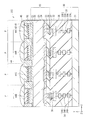
- FIG. 8 illustrates a cross-sectional configuration of a light receiving element (light receiving element 10B) according to a modification of the present disclosure.
- the light receiving element 10B of this modification includes, for example, a plurality of light receiving unit regions (referred to as pixels P) arranged two-dimensionally, for example, in the same manner as the light receiving element 10A of the above-described embodiment, for example, a visible region (for example, 380 nm or more and less than 780 nm) ) To a short infrared region (for example, 780 nm or more and less than 2400 nm) have a photoelectric conversion function.
- a visible region for example, 380 nm or more and less than 780 nm
- a short infrared region for example, 780 nm or more and less than 2400 nm
- the light receiving element 10B has a configuration in which, for example, a photoelectric conversion layer 22 and a cap layer 23 are laminated in this order on the back surface S2 side of the substrate 21 in the same manner as the light receiving element 10A.
- a protective layer 24 is further provided on the cap layer 23. Inside the protective layer 24, a contact electrode 25 electrically connected to the first conductivity type region 23A formed in the cap layer 23 is provided.
- the substrate 21 to the protective layer 24 having the contact electrode 25 are referred to as a semiconductor substrate 20.
- a plurality of transparent electrodes 41 formed separately for each pixel P are provided on the light incident surface S1 side of the substrate 21. Further, a color filter 44 and an on-chip lens 45 are further arranged in this order via a protective layer 43. Are stacked.
- a multilayer wiring substrate 30 having a readout circuit is bonded to the back surface S2 side of the semiconductor substrate 20.
- the light receiving element 10 ⁇ / b> B includes a light shielding portion 52 that separates the transparent electrode 41, the protective layer 43, and the color filter 44 between the adjacent pixels P for each pixel P.
- the light-shielding part 42 in the said embodiment and the light-shielding part 52 in a modification should just be provided at least between the adjacent pixels P, and the position of the upper end and lower end is not limited.
- the lower end of the light shielding part 52 may extend to the inside of the substrate 21. Alternatively, it may be further extended to the inside of the photoelectric conversion layer 22.
- the upper end of the light shielding portion 52 may have the same surface as the protective layer 43 without penetrating the color filter 44.
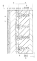
- the color filter 44 and the on-chip lens 45 are provided on the protective layer 43. However, like the light receiving element 10D shown in FIG. It can be omitted.
- FIG. 11 illustrates a functional configuration of an image pickup apparatus (image pickup element 1) using the element structure of the light receiving element 10A (or the light receiving elements 10B, 10C, and 10D) described in the above embodiments and the like.
- the imaging device 1 is, for example, an infrared image sensor, and includes, for example, a pixel unit 1a and a peripheral circuit unit 230 that drives the pixel unit 1a.
- the peripheral circuit unit 230 includes, for example, a row scanning unit 231, a horizontal selection unit 233, a column scanning unit 234, and a system control unit 232.
- the pixel unit 1a has, for example, a plurality of pixels P that are two-dimensionally arranged in a matrix.
- pixel drive lines Lread for example, row selection lines and reset control lines
- vertical signal lines Lsig are wired to the pixel columns.
- the pixel drive line Lread transmits a drive signal for reading a signal from the pixel P.
- One end of the pixel drive line Lread is connected to an output end corresponding to each row of the row scanning unit 231.
- the row scanning unit 231 includes a shift register, an address decoder, and the like, and is a pixel driving unit that drives each pixel P of the pixel unit 1a, for example, in units of rows.
- a signal output from each pixel P of the pixel row selectively scanned by the row scanning unit 231 is supplied to the horizontal selection unit 233 through each of the vertical signal lines Lsig.
- the horizontal selection unit 233 is configured by an amplifier, a horizontal selection switch, and the like provided for each vertical signal line Lsig.
- the column scanning unit 234 is configured by a shift register, an address decoder, and the like, and drives each of the horizontal selection switches of the horizontal selection unit 233 in order while scanning.
- the signal of each pixel transmitted through each of the vertical signal lines Lsig is sequentially output to the horizontal signal line 235, and is input to the signal processing unit (not shown) through the horizontal signal line 235.
- the system control unit 232 receives an externally supplied clock, data for instructing an operation mode, and the like, and outputs data such as internal information of the image sensor 1.
- the system control unit 232 further includes a timing generator that generates various timing signals, and the row scanning unit 231, the horizontal selection unit 233, the column scanning unit 234, and the like based on the various timing signals generated by the timing generator. Drive control is performed.
- FIG. 12 shows a schematic configuration of an electronic device 2 (camera) as an example.
- the electronic device 2 is a camera capable of taking a still image or a moving image, for example, and includes an image pickup device 1, an optical system (optical lens) 310, a shutter device 311, and a drive unit that drives the image pickup device 1 and the shutter device 311. 313 and a signal processing unit 312.
- the optical system 310 guides image light (incident light) from the subject to the image sensor 1.
- the optical system 310 may be composed of a plurality of optical lenses.
- the shutter device 311 controls the light irradiation period and the light shielding period to the image sensor 1.
- the drive unit 313 controls the transfer operation of the image sensor 1 and the shutter operation of the shutter device 311.
- the signal processing unit 312 performs various signal processing on the signal output from the image sensor 1.
- the video signal Dout after the signal processing is stored in a storage medium such as a memory, or is output to a monitor or the like.
- the light receiving element 10A (or the light receiving elements 10B, 10C, and 10D) described in this embodiment and the like can be applied to the following electronic devices (capsule endoscope 10100 and moving bodies such as vehicles). is there.
- FIG. 13 is a block diagram illustrating an example of a schematic configuration of an in-vivo information acquisition system for a patient using a capsule endoscope to which the technology according to the present disclosure (present technology) can be applied.
- the in-vivo information acquisition system 10001 includes a capsule endoscope 10100 and an external control device 10200.
- the capsule endoscope 10100 is swallowed by the patient at the time of examination.
- the capsule endoscope 10100 has an imaging function and a wireless communication function, and moves inside the organ such as the stomach and the intestine by peristaltic motion or the like until it is spontaneously discharged from the patient.
- Images (hereinafter also referred to as in-vivo images) are sequentially captured at predetermined intervals, and information about the in-vivo images is sequentially wirelessly transmitted to the external control device 10200 outside the body.
- the external control device 10200 comprehensively controls the operation of the in-vivo information acquisition system 10001. Further, the external control device 10200 receives information about the in-vivo image transmitted from the capsule endoscope 10100 and, based on the received information about the in-vivo image, displays the in-vivo image on the display device (not shown). The image data for displaying is generated.
- an in-vivo image obtained by imaging the inside of the patient's body can be obtained at any time in this manner until the capsule endoscope 10100 is swallowed and discharged.
- the capsule endoscope 10100 includes a capsule-type casing 10101.
- a light source unit 10111 In the casing 10101, a light source unit 10111, an imaging unit 10112, an image processing unit 10113, a wireless communication unit 10114, a power supply unit 10115, and a power supply unit 10116 and the control unit 10117 are stored.
- the light source unit 10111 includes a light source such as an LED (light-emitting diode), and irradiates the imaging field of the imaging unit 10112 with light.
- a light source such as an LED (light-emitting diode)
- the image capturing unit 10112 includes an image sensor and an optical system including a plurality of lenses provided in front of the image sensor. Reflected light (hereinafter referred to as observation light) of light irradiated on the body tissue to be observed is collected by the optical system and enters the image sensor. In the imaging unit 10112, in the imaging element, the observation light incident thereon is photoelectrically converted, and an image signal corresponding to the observation light is generated. The image signal generated by the imaging unit 10112 is provided to the image processing unit 10113.
- the image processing unit 10113 is configured by a processor such as a CPU (Central Processing Unit) or a GPU (Graphics Processing Unit), and performs various types of signal processing on the image signal generated by the imaging unit 10112.
- the image processing unit 10113 provides the radio communication unit 10114 with the image signal subjected to signal processing as RAW data.
- the wireless communication unit 10114 performs predetermined processing such as modulation processing on the image signal that has been subjected to signal processing by the image processing unit 10113, and transmits the image signal to the external control apparatus 10200 via the antenna 10114A.
- the wireless communication unit 10114 receives a control signal related to drive control of the capsule endoscope 10100 from the external control device 10200 via the antenna 10114A.
- the wireless communication unit 10114 provides a control signal received from the external control device 10200 to the control unit 10117.
- the power feeding unit 10115 includes a power receiving antenna coil, a power regeneration circuit that regenerates power from a current generated in the antenna coil, a booster circuit, and the like. In the power feeding unit 10115, electric power is generated using a so-called non-contact charging principle.
- the power supply unit 10116 is composed of a secondary battery, and stores the electric power generated by the power supply unit 10115.
- FIG. 13 in order to avoid complication of the drawing, illustration of an arrow or the like indicating a power supply destination from the power supply unit 10116 is omitted, but the power stored in the power supply unit 10116 is stored in the light source unit 10111.
- the imaging unit 10112, the image processing unit 10113, the wireless communication unit 10114, and the control unit 10117 can be used for driving them.
- the control unit 10117 includes a processor such as a CPU, and a control signal transmitted from the external control device 10200 to drive the light source unit 10111, the imaging unit 10112, the image processing unit 10113, the wireless communication unit 10114, and the power feeding unit 10115. Control accordingly.
- a processor such as a CPU
- the external control device 10200 is configured by a processor such as a CPU or GPU, or a microcomputer or a control board in which a processor and a storage element such as a memory are mounted.
- the external control device 10200 controls the operation of the capsule endoscope 10100 by transmitting a control signal to the control unit 10117 of the capsule endoscope 10100 via the antenna 10200A.
- the capsule endoscope 10100 for example, the light irradiation condition for the observation target in the light source unit 10111 can be changed by a control signal from the external control device 10200.
- an imaging condition for example, a frame rate or an exposure value in the imaging unit 10112
- a control signal from the external control device 10200 can be changed by a control signal from the external control device 10200.
- the contents of processing in the image processing unit 10113 and the conditions (for example, the transmission interval, the number of transmission images, etc.) by which the wireless communication unit 10114 transmits an image signal may be changed by a control signal from the external control device 10200. .
- the external control device 10200 performs various image processing on the image signal transmitted from the capsule endoscope 10100, and generates image data for displaying the captured in-vivo image on the display device.
- image processing for example, development processing (demosaic processing), image quality enhancement processing (band enhancement processing, super-resolution processing, NR (Noise reduction) processing and / or camera shake correction processing, etc.), and / or enlargement processing ( Various signal processing such as electronic zoom processing can be performed.
- the external control device 10200 controls driving of the display device to display an in-vivo image captured based on the generated image data.
- the external control device 10200 may cause the generated image data to be recorded on a recording device (not shown) or may be printed out on a printing device (not shown).
- the technology according to the present disclosure can be applied to, for example, the imaging unit 10112 among the configurations described above. Thereby, since a clearer surgical part image can be obtained, the accuracy of the examination is improved.
- the technology according to the present disclosure can be applied to various products.
- the technology according to the present disclosure is realized as a device that is mounted on any type of mobile body such as an automobile, an electric vehicle, a hybrid electric vehicle, a motorcycle, a bicycle, personal mobility, an airplane, a drone, a ship, and a robot. May be.
- FIG. 14 is a block diagram illustrating a schematic configuration example of a vehicle control system that is an example of a mobile control system to which the technology according to the present disclosure can be applied.
- the vehicle control system 12000 includes a plurality of electronic control units connected via a communication network 12001.
- the vehicle control system 12000 includes a drive system control unit 12010, a body system control unit 12020, a vehicle exterior information detection unit 12030, a vehicle interior information detection unit 12040, and an integrated control unit 12050.
- a microcomputer 12051, an audio image output unit 12052, and an in-vehicle network I / F (interface) 12053 are illustrated as a functional configuration of the integrated control unit 12050.
- the drive system control unit 12010 controls the operation of the device related to the drive system of the vehicle according to various programs.
- the drive system control unit 12010 includes a driving force generator for generating a driving force of a vehicle such as an internal combustion engine or a driving motor, a driving force transmission mechanism for transmitting the driving force to wheels, and a steering angle of the vehicle. It functions as a control device such as a steering mechanism that adjusts and a braking device that generates a braking force of the vehicle.
- the body system control unit 12020 controls the operation of various devices mounted on the vehicle body according to various programs.
- the body system control unit 12020 functions as a keyless entry system, a smart key system, a power window device, or a control device for various lamps such as a headlamp, a back lamp, a brake lamp, a blinker, or a fog lamp.
- the body control unit 12020 can be input with radio waves transmitted from a portable device that substitutes for a key or signals from various switches.
- the body system control unit 12020 receives input of these radio waves or signals, and controls a door lock device, a power window device, a lamp, and the like of the vehicle.
- the vehicle outside information detection unit 12030 detects information outside the vehicle on which the vehicle control system 12000 is mounted.
- the imaging unit 12031 is connected to the vehicle exterior information detection unit 12030.
- the vehicle exterior information detection unit 12030 causes the imaging unit 12031 to capture an image outside the vehicle and receives the captured image.
- the vehicle outside information detection unit 12030 may perform an object detection process or a distance detection process such as a person, a car, an obstacle, a sign, or a character on a road surface based on the received image.
- the imaging unit 12031 is an optical sensor that receives light and outputs an electrical signal corresponding to the amount of received light.
- the imaging unit 12031 can output an electrical signal as an image, or can output it as distance measurement information. Further, the light received by the imaging unit 12031 may be visible light or invisible light such as infrared rays.
- the vehicle interior information detection unit 12040 detects vehicle interior information.
- a driver state detection unit 12041 that detects a driver's state is connected to the in-vehicle information detection unit 12040.
- the driver state detection unit 12041 includes, for example, a camera that images the driver, and the vehicle interior information detection unit 12040 determines the degree of fatigue or concentration of the driver based on the detection information input from the driver state detection unit 12041. It may be calculated or it may be determined whether the driver is asleep.
- the microcomputer 12051 calculates a control target value of the driving force generator, the steering mechanism, or the braking device based on the information inside / outside the vehicle acquired by the vehicle outside information detection unit 12030 or the vehicle interior information detection unit 12040, and the drive system control unit A control command can be output to 12010.
- the microcomputer 12051 realizes ADAS (Advanced Driver Assistance System) functions including vehicle collision avoidance or impact mitigation, following traveling based on inter-vehicle distance, vehicle speed maintenance traveling, vehicle collision warning, or vehicle lane departure warning. It is possible to perform cooperative control for the purpose.
- ADAS Advanced Driver Assistance System
- the microcomputer 12051 controls the driving force generator, the steering mechanism, the braking device, and the like based on the information around the vehicle acquired by the vehicle exterior information detection unit 12030 or the vehicle interior information detection unit 12040. It is possible to perform cooperative control for the purpose of automatic driving that autonomously travels without depending on the operation.
- the microcomputer 12051 can output a control command to the body system control unit 12020 based on information outside the vehicle acquired by the vehicle outside information detection unit 12030.
- the microcomputer 12051 controls the headlamp according to the position of the preceding vehicle or the oncoming vehicle detected by the outside information detection unit 12030, and performs cooperative control for the purpose of anti-glare, such as switching from a high beam to a low beam. It can be carried out.
- the sound image output unit 12052 transmits an output signal of at least one of sound and image to an output device capable of visually or audibly notifying information to a vehicle occupant or the outside of the vehicle.
- an audio speaker 12061, a display unit 12062, and an instrument panel 12063 are illustrated as output devices.
- the display unit 12062 may include at least one of an on-board display and a head-up display, for example.
- FIG. 15 is a diagram illustrating an example of an installation position of the imaging unit 12031.
- the imaging unit 12031 includes imaging units 12101, 12102, 12103, 12104, and 12105.
- the imaging units 12101, 12102, 12103, 12104, and 12105 are provided, for example, at positions such as a front nose, a side mirror, a rear bumper, a back door, and an upper part of a windshield in the vehicle interior of the vehicle 12100.
- the imaging unit 12101 provided in the front nose and the imaging unit 12105 provided in the upper part of the windshield in the vehicle interior mainly acquire an image in front of the vehicle 12100.
- the imaging units 12102 and 12103 provided in the side mirror mainly acquire an image of the side of the vehicle 12100.
- the imaging unit 12104 provided in the rear bumper or the back door mainly acquires an image behind the vehicle 12100.
- the imaging unit 12105 provided on the upper part of the windshield in the passenger compartment is mainly used for detecting a preceding vehicle or a pedestrian, an obstacle, a traffic light, a traffic sign, a lane, or the like.
- FIG. 15 shows an example of the shooting range of the imaging units 12101 to 12104.
- the imaging range 12111 indicates the imaging range of the imaging unit 12101 provided in the front nose
- the imaging ranges 12112 and 12113 indicate the imaging ranges of the imaging units 12102 and 12103 provided in the side mirrors, respectively
- the imaging range 12114 The imaging range of the imaging part 12104 provided in the rear bumper or the back door is shown. For example, by superimposing the image data captured by the imaging units 12101 to 12104, an overhead image when the vehicle 12100 is viewed from above is obtained.
- At least one of the imaging units 12101 to 12104 may have a function of acquiring distance information.
- at least one of the imaging units 12101 to 12104 may be a stereo camera including a plurality of imaging elements, or may be an imaging element having pixels for phase difference detection.
- the microcomputer 12051 based on the distance information obtained from the imaging units 12101 to 12104, the distance to each three-dimensional object in the imaging range 12111 to 12114 and the temporal change in this distance (relative speed with respect to the vehicle 12100).
- a predetermined speed for example, 0 km / h or more
- the microcomputer 12051 can set an inter-vehicle distance to be secured in advance before the preceding vehicle, and can perform automatic brake control (including follow-up stop control), automatic acceleration control (including follow-up start control), and the like.
- automatic brake control including follow-up stop control
- automatic acceleration control including follow-up start control
- cooperative control for the purpose of autonomous driving or the like autonomously traveling without depending on the operation of the driver can be performed.
- the microcomputer 12051 converts the three-dimensional object data related to the three-dimensional object to other three-dimensional objects such as a two-wheeled vehicle, a normal vehicle, a large vehicle, a pedestrian, and a utility pole based on the distance information obtained from the imaging units 12101 to 12104. It can be classified and extracted and used for automatic avoidance of obstacles.
- the microcomputer 12051 identifies obstacles around the vehicle 12100 as obstacles that are visible to the driver of the vehicle 12100 and obstacles that are difficult to see.
- the microcomputer 12051 determines the collision risk indicating the risk of collision with each obstacle, and when the collision risk is equal to or higher than the set value and there is a possibility of collision, the microcomputer 12051 is connected via the audio speaker 12061 or the display unit 12062. By outputting an alarm to the driver and performing forced deceleration or avoidance steering via the drive system control unit 12010, driving assistance for collision avoidance can be performed.
- At least one of the imaging units 12101 to 12104 may be an infrared camera that detects infrared rays.
- the microcomputer 12051 can recognize a pedestrian by determining whether a pedestrian is present in the captured images of the imaging units 12101 to 12104. Such pedestrian recognition is, for example, whether or not the user is a pedestrian by performing a pattern matching process on a sequence of feature points indicating the outline of an object and a procedure for extracting feature points in the captured images of the imaging units 12101 to 12104 as infrared cameras. It is carried out by the procedure for determining.
- the audio image output unit 12052 When the microcomputer 12051 determines that there is a pedestrian in the captured images of the imaging units 12101 to 12104 and recognizes the pedestrian, the audio image output unit 12052 has a rectangular contour line for emphasizing the recognized pedestrian.
- the display unit 12062 is controlled so as to be superimposed and displayed.
- voice image output part 12052 may control the display part 12062 so that the icon etc. which show a pedestrian may be displayed on a desired position.
- the technique according to the present disclosure can be applied to, for example, the imaging unit 12031 among the configurations described above.
- the technique according to the present disclosure By applying the technique according to the present disclosure to the imaging unit 12031, it is possible to obtain a captured image that is easier to see, and thus it is possible to reduce driver fatigue.
- the layer configuration of the light receiving element 10A (or the light receiving elements 10B, 10C, and 10D) described in the above embodiments and the like is merely an example, and other layers may be provided.
- the material and thickness of each layer are examples, and are not limited to those described above.
- the light-shielding part 42 (and the light-shielding part 52) described in the above embodiments and the like do not necessarily have to be formed between all adjacent pixels P.
- the present invention is not limited thereto.
- the present technology can be applied to a light-receiving element configured using an organic semiconductor, and the same effects as those described in the above-described embodiment and the like can be obtained.
- the present disclosure may be configured as follows. (1) A plurality of pixels; A common photoelectric conversion layer for the plurality of pixels; A first electrode layer provided on the light incident surface side of the photoelectric conversion layer; A light-receiving element comprising: a light-shielding portion embedded between the plurality of adjacent pixels of the first electrode layer.
- the said photoelectric converting layer is a light receiving element as described in said (1) which absorbs the wavelength of an infrared region at least and generate
- the photoelectric conversion layer has a second semiconductor layer on a surface opposite to the first semiconductor layer,
- the said 2nd semiconductor layer has a 1st conductivity type area
- Light receiving element (9)
- the first conductivity type region is provided for each of the plurality of pixels, The light receiving element according to (8), wherein the plurality of adjacent pixels are electrically separated by a boundary between the first conductivity type region and the second conductivity type region.
- the second semiconductor layer has a second electrode between the multilayer wiring board, The light receiving element according to (10), wherein the first conductivity type region and the readout circuit are electrically connected via the second electrode.
- the photoelectric conversion layer is made of In x Ga (1-x) As (0 ⁇ x ⁇ 1), The light receiving element according to any one of (8) to (13), wherein the first semiconductor layer and the second semiconductor layer are made of InP or InGaAs.
- the first electrode layer includes indium titanium oxide (ITO).
- the first electrode layer has a plurality of slits in a plane.
- the protective layer is configured by a silicon nitride (SiN x ) film or a silicon oxide (SiO x ) film.
- An imaging device comprising: a light shielding portion embedded between the plurality of adjacent pixels of the first electrode layer.
Landscapes
- Solid State Image Pick-Up Elements (AREA)
- Electrodes Of Semiconductors (AREA)
- Light Receiving Elements (AREA)
- Transforming Light Signals Into Electric Signals (AREA)
Abstract
Priority Applications (6)
| Application Number | Priority Date | Filing Date | Title |
|---|---|---|---|
| US16/316,670 US10818718B2 (en) | 2016-07-20 | 2017-05-26 | Light receiving element, method of manufacturing light receiving element, imaging device, and electronic apparatus |
| EP17830701.3A EP3490001B1 (fr) | 2016-07-20 | 2017-05-26 | Élément de réception de lumière, procédé de fabrication d'élément de réception de lumière, appareil d'imagerie et dispositif électronique |
| JP2018528427A JP6943245B2 (ja) | 2016-07-20 | 2017-05-26 | 受光素子、撮像装置および電子機器 |
| CN201780038461.XA CN109314124B (zh) | 2016-07-20 | 2017-05-26 | 受光元件及其制造方法、成像器件和电子装置 |
| CN202310293532.8A CN116404020A (zh) | 2016-07-20 | 2017-05-26 | 受光元件及其制造方法、成像器件和电子装置 |
| KR1020187034997A KR102413726B1 (ko) | 2016-07-20 | 2017-05-26 | 수광 소자, 수광 소자의 제조 방법, 촬상 장치 및 전자 기기 |
Applications Claiming Priority (2)
| Application Number | Priority Date | Filing Date | Title |
|---|---|---|---|
| JP2016-142826 | 2016-07-20 | ||
| JP2016142826 | 2016-07-20 |
Publications (1)
| Publication Number | Publication Date |
|---|---|
| WO2018016181A1 true WO2018016181A1 (fr) | 2018-01-25 |
Family
ID=60992068
Family Applications (1)
| Application Number | Title | Priority Date | Filing Date |
|---|---|---|---|
| PCT/JP2017/019731 Ceased WO2018016181A1 (fr) | 2016-07-20 | 2017-05-26 | Élément de réception de lumière, procédé de fabrication d'élément de réception de lumière, appareil d'imagerie et dispositif électronique |
Country Status (6)
| Country | Link |
|---|---|
| US (1) | US10818718B2 (fr) |
| EP (1) | EP3490001B1 (fr) |
| JP (1) | JP6943245B2 (fr) |
| KR (1) | KR102413726B1 (fr) |
| CN (2) | CN109314124B (fr) |
| WO (1) | WO2018016181A1 (fr) |
Cited By (6)
| Publication number | Priority date | Publication date | Assignee | Title |
|---|---|---|---|---|
| WO2020059495A1 (fr) * | 2018-09-19 | 2020-03-26 | ソニーセミコンダクタソリューションズ株式会社 | Élément d'imagerie, élément à semi-conducteurs, et dispositif électronique |
| WO2020080124A1 (fr) * | 2018-10-16 | 2020-04-23 | ソニーセミコンダクタソリューションズ株式会社 | Élément semi-conducteur et son procédé de fabrication |
| JPWO2020137282A1 (ja) * | 2018-12-28 | 2021-11-11 | ソニーセミコンダクタソリューションズ株式会社 | 撮像素子および電子機器 |
| WO2021240998A1 (fr) * | 2020-05-26 | 2021-12-02 | ソニーセミコンダクタソリューションズ株式会社 | Élément d'imagerie à semi-conducteurs |
| WO2022249734A1 (fr) * | 2021-05-28 | 2022-12-01 | ソニーセミコンダクタソリューションズ株式会社 | Dispositif d'imagerie et appareil électronique |
| JPWO2023149195A1 (fr) * | 2022-02-01 | 2023-08-10 |
Families Citing this family (10)
| Publication number | Priority date | Publication date | Assignee | Title |
|---|---|---|---|---|
| JP6754157B2 (ja) * | 2015-10-26 | 2020-09-09 | ソニーセミコンダクタソリューションズ株式会社 | 撮像装置 |
| KR102369603B1 (ko) * | 2017-08-21 | 2022-03-02 | 양쯔 메모리 테크놀로지스 씨오., 엘티디. | 3차원 메모리 장치 및 그 형성 방법 |
| CN110098203B (zh) * | 2018-01-30 | 2024-09-24 | 维深半导体公司 | 背照式图像传感器及其制备 |
| WO2019198385A1 (fr) | 2018-04-09 | 2019-10-17 | ソニーセミコンダクタソリューションズ株式会社 | Dispositif de capture d'image, son procédé de fabrication, et dispositif électronique |
| KR102553314B1 (ko) | 2018-08-29 | 2023-07-10 | 삼성전자주식회사 | 이미지 센서 |
| CN110087005B (zh) * | 2019-04-23 | 2021-07-09 | Oppo广东移动通信有限公司 | 一种彩色偏振式cis及图像处理方法、存储介质 |
| WO2021100298A1 (fr) * | 2019-11-21 | 2021-05-27 | ソニーセミコンダクタソリューションズ株式会社 | Élément d'imagerie et dispositif d'imagerie |
| KR102812791B1 (ko) | 2020-03-02 | 2025-05-23 | 삼성전자주식회사 | 이미지 센서 |
| JP7580708B2 (ja) * | 2020-04-14 | 2024-11-12 | 株式会社ノベルクリスタルテクノロジー | 半導体膜及びその製造方法 |
| US11699768B1 (en) * | 2022-03-29 | 2023-07-11 | Visera Technologies Company Ltd. | Patterned electrode structure for image sensor |
Citations (5)
| Publication number | Priority date | Publication date | Assignee | Title |
|---|---|---|---|---|
| JPS62219567A (ja) * | 1986-03-19 | 1987-09-26 | Fujitsu Ltd | 薄膜素子 |
| JP2010067827A (ja) * | 2008-09-11 | 2010-03-25 | Fujifilm Corp | 固体撮像素子及び撮像装置 |
| JP2014060380A (ja) * | 2012-06-14 | 2014-04-03 | Rohm Co Ltd | 光電変換装置 |
| JP2015149422A (ja) * | 2014-02-07 | 2015-08-20 | ソニー株式会社 | 受光素子、撮像素子及び撮像装置 |
| JP2016058559A (ja) * | 2014-09-10 | 2016-04-21 | ソニー株式会社 | 固体撮像装置およびその駆動方法、並びに電子機器 |
Family Cites Families (10)
| Publication number | Priority date | Publication date | Assignee | Title |
|---|---|---|---|---|
| JP4122739B2 (ja) * | 2001-07-26 | 2008-07-23 | 松下電工株式会社 | 発光素子及びその製造方法 |
| CN101228631A (zh) * | 2005-06-02 | 2008-07-23 | 索尼株式会社 | 半导体图像传感器模块及其制造方法 |
| JP5196739B2 (ja) * | 2006-06-09 | 2013-05-15 | キヤノン株式会社 | 放射線撮像装置及び放射線撮像システム |
| US8207589B2 (en) * | 2007-02-15 | 2012-06-26 | Semiconductor Energy Laboratory Co., Ltd. | Photoelectric conversion device and electronic device, and method for manufacturing photoelectric conversion device |
| JP5198150B2 (ja) * | 2008-05-29 | 2013-05-15 | 株式会社東芝 | 固体撮像装置 |
| KR20090128899A (ko) * | 2008-06-11 | 2009-12-16 | 크로스텍 캐피탈, 엘엘씨 | 후면 조사 이미지 센서 및 그 제조방법 |
| JP2010232387A (ja) * | 2009-03-26 | 2010-10-14 | Panasonic Corp | 固体撮像素子 |
| JP5536488B2 (ja) * | 2010-02-22 | 2014-07-02 | ローム株式会社 | カラー用固体撮像装置 |
| US9543346B2 (en) * | 2013-03-29 | 2017-01-10 | Sony Corporation | Imaging element and imaging device |
| JP6521586B2 (ja) * | 2014-07-31 | 2019-05-29 | キヤノン株式会社 | 固体撮像素子および撮像システム |
-
2017
- 2017-05-26 US US16/316,670 patent/US10818718B2/en active Active
- 2017-05-26 WO PCT/JP2017/019731 patent/WO2018016181A1/fr not_active Ceased
- 2017-05-26 EP EP17830701.3A patent/EP3490001B1/fr not_active Not-in-force
- 2017-05-26 KR KR1020187034997A patent/KR102413726B1/ko not_active Expired - Fee Related
- 2017-05-26 CN CN201780038461.XA patent/CN109314124B/zh active Active
- 2017-05-26 JP JP2018528427A patent/JP6943245B2/ja active Active
- 2017-05-26 CN CN202310293532.8A patent/CN116404020A/zh not_active Withdrawn
Patent Citations (5)
| Publication number | Priority date | Publication date | Assignee | Title |
|---|---|---|---|---|
| JPS62219567A (ja) * | 1986-03-19 | 1987-09-26 | Fujitsu Ltd | 薄膜素子 |
| JP2010067827A (ja) * | 2008-09-11 | 2010-03-25 | Fujifilm Corp | 固体撮像素子及び撮像装置 |
| JP2014060380A (ja) * | 2012-06-14 | 2014-04-03 | Rohm Co Ltd | 光電変換装置 |
| JP2015149422A (ja) * | 2014-02-07 | 2015-08-20 | ソニー株式会社 | 受光素子、撮像素子及び撮像装置 |
| JP2016058559A (ja) * | 2014-09-10 | 2016-04-21 | ソニー株式会社 | 固体撮像装置およびその駆動方法、並びに電子機器 |
Cited By (16)
| Publication number | Priority date | Publication date | Assignee | Title |
|---|---|---|---|---|
| WO2020059495A1 (fr) * | 2018-09-19 | 2020-03-26 | ソニーセミコンダクタソリューションズ株式会社 | Élément d'imagerie, élément à semi-conducteurs, et dispositif électronique |
| JP7653788B2 (ja) | 2018-09-19 | 2025-03-31 | ソニーセミコンダクタソリューションズ株式会社 | 撮像素子および電子機器 |
| JPWO2020059495A1 (ja) * | 2018-09-19 | 2021-09-24 | ソニーセミコンダクタソリューションズ株式会社 | 撮像素子、半導体素子および電子機器 |
| US11961863B2 (en) | 2018-09-19 | 2024-04-16 | Sony Semiconductor Solutions Corporation | Imaging element, semiconductor element, and electronic apparatus |
| JP7372258B2 (ja) | 2018-10-16 | 2023-10-31 | ソニーセミコンダクタソリューションズ株式会社 | 半導体素子およびその製造方法 |
| JP2024012345A (ja) * | 2018-10-16 | 2024-01-30 | ソニーセミコンダクタソリューションズ株式会社 | 半導体素子およびその製造方法 |
| JPWO2020080124A1 (ja) * | 2018-10-16 | 2021-09-30 | ソニーセミコンダクタソリューションズ株式会社 | 半導体素子およびその製造方法 |
| US12027557B2 (en) | 2018-10-16 | 2024-07-02 | Sony Semiconductor Solutions Corporation | Semiconductor element and method of manufacturing the same |
| WO2020080124A1 (fr) * | 2018-10-16 | 2020-04-23 | ソニーセミコンダクタソリューションズ株式会社 | Élément semi-conducteur et son procédé de fabrication |
| JP7660642B2 (ja) | 2018-10-16 | 2025-04-11 | ソニーセミコンダクタソリューションズ株式会社 | 半導体素子 |
| JPWO2020137282A1 (ja) * | 2018-12-28 | 2021-11-11 | ソニーセミコンダクタソリューションズ株式会社 | 撮像素子および電子機器 |
| WO2021240998A1 (fr) * | 2020-05-26 | 2021-12-02 | ソニーセミコンダクタソリューションズ株式会社 | Élément d'imagerie à semi-conducteurs |
| US12604544B2 (en) | 2020-05-26 | 2026-04-14 | Sony Semiconductor Solutions Corporation | Solid-state imaging element |
| WO2022249734A1 (fr) * | 2021-05-28 | 2022-12-01 | ソニーセミコンダクタソリューションズ株式会社 | Dispositif d'imagerie et appareil électronique |
| JPWO2023149195A1 (fr) * | 2022-02-01 | 2023-08-10 | ||
| JP7806101B2 (ja) | 2022-02-01 | 2026-01-26 | 株式会社Magnolia White | 検出装置 |
Also Published As
| Publication number | Publication date |
|---|---|
| CN109314124B (zh) | 2023-05-12 |
| JP6943245B2 (ja) | 2021-09-29 |
| EP3490001A4 (fr) | 2019-07-03 |
| CN116404020A (zh) | 2023-07-07 |
| EP3490001B1 (fr) | 2020-07-15 |
| EP3490001A1 (fr) | 2019-05-29 |
| JPWO2018016181A1 (ja) | 2019-05-09 |
| CN109314124A (zh) | 2019-02-05 |
| KR102413726B1 (ko) | 2022-06-28 |
| US20190157324A1 (en) | 2019-05-23 |
| US10818718B2 (en) | 2020-10-27 |
| KR20190028376A (ko) | 2019-03-18 |
Similar Documents
| Publication | Publication Date | Title |
|---|---|---|
| JP6943245B2 (ja) | 受光素子、撮像装置および電子機器 | |
| US11646341B2 (en) | Light-receiving device, method of manufacturing light-receiving device, and electronic apparatus | |
| KR102400664B1 (ko) | 수광 소자, 수광 소자의 제조 방법, 촬상 소자 및 전자 기기 | |
| US12396279B2 (en) | Solid-state image pickup apparatus and electronic equipment | |
| KR102538710B1 (ko) | 수광소자, 촬상소자 및 전자기기 | |
| KR102609022B1 (ko) | 수광 소자, 수광 소자의 제조 방법, 촬상 소자 및 전자 기기 | |
| CN111433914B (zh) | 受光元件和电子装置 | |
| US11728361B2 (en) | Imaging device and manufacturing method thereof | |
| CN108475688B (zh) | 受光元件、受光元件的制造方法、成像元件以及电子设备 | |
| WO2019009024A1 (fr) | Élément imageur et dispositif imageur | |
| WO2024154646A1 (fr) | Dispositif photodétecteur et procédé de fabrication de dispositif photodétecteur | |
| CN117157763A (zh) | 光检测装置、光检测系统、电子设备和移动体 | |
| US20240395833A1 (en) | Photoelectric conversion element and imaging device | |
| WO2024135105A1 (fr) | Élément de photodétection et appareil électronique | |
| US20240136381A1 (en) | Imaging device and electronic apparatus | |
| WO2023002592A1 (fr) | Élément d'imagerie à semi-conducteurs, son procédé de fabrication et appareil électronique |
Legal Events
| Date | Code | Title | Description |
|---|---|---|---|
| ENP | Entry into the national phase |
Ref document number: 20187034997 Country of ref document: KR Kind code of ref document: A |
|
| 121 | Ep: the epo has been informed by wipo that ep was designated in this application |
Ref document number: 17830701 Country of ref document: EP Kind code of ref document: A1 |
|
| ENP | Entry into the national phase |
Ref document number: 2018528427 Country of ref document: JP Kind code of ref document: A |
|
| NENP | Non-entry into the national phase |
Ref country code: DE |
|
| ENP | Entry into the national phase |
Ref document number: 2017830701 Country of ref document: EP Effective date: 20190220 |