WO2018016430A1 - Système d'inspection combiné - Google Patents
Système d'inspection combiné Download PDFInfo
- Publication number
- WO2018016430A1 WO2018016430A1 PCT/JP2017/025676 JP2017025676W WO2018016430A1 WO 2018016430 A1 WO2018016430 A1 WO 2018016430A1 JP 2017025676 W JP2017025676 W JP 2017025676W WO 2018016430 A1 WO2018016430 A1 WO 2018016430A1
- Authority
- WO
- WIPO (PCT)
- Prior art keywords
- sample
- ray
- unit
- inspection
- inspection apparatus
- Prior art date
- Legal status (The legal status is an assumption and is not a legal conclusion. Google has not performed a legal analysis and makes no representation as to the accuracy of the status listed.)
- Ceased
Links
Images


Classifications
-
- G—PHYSICS
- G01—MEASURING; TESTING
- G01N—INVESTIGATING OR ANALYSING MATERIALS BY DETERMINING THEIR CHEMICAL OR PHYSICAL PROPERTIES
- G01N23/00—Investigating or analysing materials by the use of wave or particle radiation, e.g. X-rays or neutrons, not covered by groups G01N3/00 – G01N17/00, G01N21/00 or G01N22/00
- G01N23/20—Investigating or analysing materials by the use of wave or particle radiation, e.g. X-rays or neutrons, not covered by groups G01N3/00 – G01N17/00, G01N21/00 or G01N22/00 by using diffraction of the radiation by the materials, e.g. for investigating crystal structure; by using scattering of the radiation by the materials, e.g. for investigating non-crystalline materials; by using reflection of the radiation by the materials
- G01N23/20008—Constructional details of analysers, e.g. characterised by X-ray source, detector or optical system; Accessories therefor; Preparing specimens therefor
- G01N23/20025—Sample holders or supports therefor
-
- G—PHYSICS
- G01—MEASURING; TESTING
- G01N—INVESTIGATING OR ANALYSING MATERIALS BY DETERMINING THEIR CHEMICAL OR PHYSICAL PROPERTIES
- G01N23/00—Investigating or analysing materials by the use of wave or particle radiation, e.g. X-rays or neutrons, not covered by groups G01N3/00 – G01N17/00, G01N21/00 or G01N22/00
- G01N23/20—Investigating or analysing materials by the use of wave or particle radiation, e.g. X-rays or neutrons, not covered by groups G01N3/00 – G01N17/00, G01N21/00 or G01N22/00 by using diffraction of the radiation by the materials, e.g. for investigating crystal structure; by using scattering of the radiation by the materials, e.g. for investigating non-crystalline materials; by using reflection of the radiation by the materials
- G01N23/201—Investigating or analysing materials by the use of wave or particle radiation, e.g. X-rays or neutrons, not covered by groups G01N3/00 – G01N17/00, G01N21/00 or G01N22/00 by using diffraction of the radiation by the materials, e.g. for investigating crystal structure; by using scattering of the radiation by the materials, e.g. for investigating non-crystalline materials; by using reflection of the radiation by the materials by measuring small-angle scattering
-
- G—PHYSICS
- G01—MEASURING; TESTING
- G01N—INVESTIGATING OR ANALYSING MATERIALS BY DETERMINING THEIR CHEMICAL OR PHYSICAL PROPERTIES
- G01N23/00—Investigating or analysing materials by the use of wave or particle radiation, e.g. X-rays or neutrons, not covered by groups G01N3/00 – G01N17/00, G01N21/00 or G01N22/00
- G01N23/20—Investigating or analysing materials by the use of wave or particle radiation, e.g. X-rays or neutrons, not covered by groups G01N3/00 – G01N17/00, G01N21/00 or G01N22/00 by using diffraction of the radiation by the materials, e.g. for investigating crystal structure; by using scattering of the radiation by the materials, e.g. for investigating non-crystalline materials; by using reflection of the radiation by the materials
- G01N23/20008—Constructional details of analysers, e.g. characterised by X-ray source, detector or optical system; Accessories therefor; Preparing specimens therefor
- G01N23/20016—Goniometers
-
- G—PHYSICS
- G01—MEASURING; TESTING
- G01N—INVESTIGATING OR ANALYSING MATERIALS BY DETERMINING THEIR CHEMICAL OR PHYSICAL PROPERTIES
- G01N23/00—Investigating or analysing materials by the use of wave or particle radiation, e.g. X-rays or neutrons, not covered by groups G01N3/00 – G01N17/00, G01N21/00 or G01N22/00
- G01N23/20—Investigating or analysing materials by the use of wave or particle radiation, e.g. X-rays or neutrons, not covered by groups G01N3/00 – G01N17/00, G01N21/00 or G01N22/00 by using diffraction of the radiation by the materials, e.g. for investigating crystal structure; by using scattering of the radiation by the materials, e.g. for investigating non-crystalline materials; by using reflection of the radiation by the materials
- G01N23/203—Measuring back scattering
-
- G—PHYSICS
- G01—MEASURING; TESTING
- G01N—INVESTIGATING OR ANALYSING MATERIALS BY DETERMINING THEIR CHEMICAL OR PHYSICAL PROPERTIES
- G01N21/00—Investigating or analysing materials by the use of optical means, i.e. using sub-millimetre waves, infrared, visible or ultraviolet light
- G01N21/84—Systems specially adapted for particular applications
- G01N21/88—Investigating the presence of flaws or contamination
- G01N21/95—Investigating the presence of flaws or contamination characterised by the material or shape of the object to be examined
- G01N21/9501—Semiconductor wafers
-
- G—PHYSICS
- G01—MEASURING; TESTING
- G01N—INVESTIGATING OR ANALYSING MATERIALS BY DETERMINING THEIR CHEMICAL OR PHYSICAL PROPERTIES
- G01N2223/00—Investigating materials by wave or particle radiation
- G01N2223/045—Investigating materials by wave or particle radiation combination of at least 2 measurements (transmission and scatter)
-
- G—PHYSICS
- G01—MEASURING; TESTING
- G01N—INVESTIGATING OR ANALYSING MATERIALS BY DETERMINING THEIR CHEMICAL OR PHYSICAL PROPERTIES
- G01N2223/00—Investigating materials by wave or particle radiation
- G01N2223/05—Investigating materials by wave or particle radiation by diffraction, scatter or reflection
- G01N2223/054—Investigating materials by wave or particle radiation by diffraction, scatter or reflection small angle scatter
-
- G—PHYSICS
- G01—MEASURING; TESTING
- G01N—INVESTIGATING OR ANALYSING MATERIALS BY DETERMINING THEIR CHEMICAL OR PHYSICAL PROPERTIES
- G01N2223/00—Investigating materials by wave or particle radiation
- G01N2223/10—Different kinds of radiation or particles
- G01N2223/101—Different kinds of radiation or particles electromagnetic radiation
- G01N2223/1016—X-ray
-
- G—PHYSICS
- G01—MEASURING; TESTING
- G01N—INVESTIGATING OR ANALYSING MATERIALS BY DETERMINING THEIR CHEMICAL OR PHYSICAL PROPERTIES
- G01N2223/00—Investigating materials by wave or particle radiation
- G01N2223/30—Accessories, mechanical or electrical features
- G01N2223/304—Accessories, mechanical or electrical features electric circuits, signal processing
-
- G—PHYSICS
- G01—MEASURING; TESTING
- G01N—INVESTIGATING OR ANALYSING MATERIALS BY DETERMINING THEIR CHEMICAL OR PHYSICAL PROPERTIES
- G01N2223/00—Investigating materials by wave or particle radiation
- G01N2223/30—Accessories, mechanical or electrical features
- G01N2223/321—Accessories, mechanical or electrical features manipulator for positioning a part
-
- G—PHYSICS
- G01—MEASURING; TESTING
- G01N—INVESTIGATING OR ANALYSING MATERIALS BY DETERMINING THEIR CHEMICAL OR PHYSICAL PROPERTIES
- G01N2223/00—Investigating materials by wave or particle radiation
- G01N2223/60—Specific applications or type of materials
- G01N2223/611—Specific applications or type of materials patterned objects; electronic devices
- G01N2223/6116—Specific applications or type of materials patterned objects; electronic devices semiconductor wafer
-
- H—ELECTRICITY
- H10—SEMICONDUCTOR DEVICES; ELECTRIC SOLID-STATE DEVICES NOT OTHERWISE PROVIDED FOR
- H10P—GENERIC PROCESSES OR APPARATUS FOR THE MANUFACTURE OR TREATMENT OF DEVICES COVERED BY CLASS H10
- H10P74/00—Testing or measuring during manufacture or treatment of wafers, substrates or devices
- H10P74/20—Testing or measuring during manufacture or treatment of wafers, substrates or devices characterised by the properties tested or measured, e.g. structural or electrical properties
- H10P74/203—Structural properties, e.g. testing or measuring thicknesses, line widths, warpage, bond strengths or physical defects
Definitions
- the present invention relates to a composite inspection system suitable for a technical field of manufacturing an element having a multilayer film structure in which a large number of thin films are laminated on a substrate, such as a semiconductor manufacturing field.
- the shape of this kind of processed element is called CD (Critical Dimension) as an important numerical value to be managed in the semiconductor process.
- TEMs transmission electron microscopes
- SEMs scanning electron microscopes
- an inspection apparatus for measuring the shape of the element as described above in-line in a non-destructive manner in a semiconductor manufacturing process an inspection apparatus using a scanning electron microscope (CD-SEM: Optical Dimension-Scanning Electron Microscope), an optical technique
- CD-SEM Optical Dimension-Scanning Electron Microscope
- OCD Optical Critical Dimension
- CD-AFM Critical Dimension Atomic Force Microscope
- an X-ray nano-shape measurement device (CD-SAXS: Critical Dimension Small Angle X-ray Scattering) using small-angle X-ray scattering has been proposed as an inspection device that accurately determines repeated pattern shapes using X-rays.
- Patent Documents 1 and 2 disclose conventional examples of CD-SAXS.
- the OCD described above has advantages such as a small measurement area and high throughput due to the use of light as a probe, and features that can analyze complex three-dimensional structures of semiconductor devices using modeling and simulation. Therefore, it is effective as an inspection apparatus for in-line measurement in the semiconductor manufacturing process.
- the CD-SEM is effective as an inspection apparatus for directly observing the device surface shape using the principle of a scanning electron microscope.
- these inspection apparatuses have a limit of resolution on a scale with a pitch of 10 nm or less, and analysis becomes difficult as the semiconductor elements are miniaturized.
- CD-SAXS is effective as an inspection device that analyzes the nanometer-scale shape of the surface of an electronic device.
- a powerful X-ray source is required, and a compact high-intensity X-ray source suitable for a semiconductor in-line inspection apparatus has not been obtained.
- the present invention has been made in view of the circumstances of these prior arts, and an object thereof is to provide a composite inspection system suitable for shape analysis of an element having a multilayer film structure in which a large number of thin films are laminated on a substrate, such as a semiconductor element. .
- Non-Patent Document 1 The basic concept of this type of combined inspection system is disclosed in Non-Patent Document 1, and the present invention is embodied based on this basic concept.
- the present invention includes a first inspection apparatus that inspects a sample based on X-ray measurement data obtained by irradiating the sample with X-rays, and a second inspection that inspects the sample by a measurement technique that does not use X-rays.
- a combined inspection system comprising: One of the X-ray measurement data obtained by the first inspection apparatus and the analysis result of the X-ray measurement data is output to the second inspection apparatus, The second inspection apparatus is characterized by inspecting a sample by using one of the X-ray measurement data obtained by the first inspection apparatus and the analysis result of the X-ray measurement data.
- the first inspection apparatus is A measurement unit that irradiates the surface of the sample with X-rays and measures the scattering intensity;
- the fine structure on the surface of the sample forms a plurality of layers having different refractive indexes in a direction perpendicular to the surface, and a periodic structure in which unit structures are periodically arranged in a direction parallel to the surface in the layer.
- the scattering intensity of X-rays scattered by the fine structure was calculated, and the X-ray scattering intensity calculated by the sample model was measured.
- a fitting section for fitting to the scattering intensity A determination unit that determines an optimum value of a parameter for specifying the shape of the unit structure based on a fitting result of the fitting unit; An output unit that outputs at least part of an analysis value including an optimum value of a parameter that specifies the shape of the unit structure as an output value according to a predetermined protocol, and a second inspection apparatus,
- the second inspection apparatus can be configured to inspect the sample using the output value from the first inspection apparatus.
- the first inspection device A measurement unit that irradiates the surface of the sample with X-rays and measures the scattering intensity;
- the fine structure on the surface forms one or a plurality of layers in a direction perpendicular to the surface, and unit structures are periodically arranged in the layer in a direction parallel to the surface, and the unit structure Is assumed to have a sample model that constitutes a periodic structure that has random position fluctuations from a strict periodic position, and the position fluctuations are not dependent on mutual position differences, and are random.
- the unit structure is formed by uniform solid regions and spatial regions in the layer, the X-ray scattering intensity generated by the solid region is calculated, and the X-ray scattering intensity calculated by the sample model is measured.
- a fitting part to be fitted to A determination unit that determines an optimum value of a parameter for specifying the shape of the unit structure based on a fitting result of the fitting unit; An output unit that outputs at least part of an analysis value including an optimum value of a parameter that specifies the shape of the unit structure as an output value according to a predetermined protocol, and a second inspection apparatus,
- the second inspection apparatus may be configured to inspect the sample using an output value from the first inspection apparatus.
- position fluctuation refers to a deviation (variation) from a position (strict periodic position) where the unit structure should be.
- the “substance region” refers to a region where a substance (basically a solid) exists in the unit structure.
- the “space region” refers to a region where no substance (basically solid) exists in the unit structure. Gas is also present in the space region.
- the present invention also provides a first inspection apparatus that inspects a sample based on X-ray measurement data obtained by irradiating the sample with X-rays, and a second inspection that inspects the sample by a measurement technique that does not use X-rays.
- a combined inspection system including an inspection device, One of the measurement data obtained by the second inspection device and the analysis result of the measurement data is output to the first inspection device;
- the first inspection apparatus may be configured to inspect the sample using one of the measurement data obtained by the second inspection apparatus and the analysis result of the measurement data.
- the present invention also provides a first inspection apparatus for inspecting a sample based on X-ray measurement data obtained by irradiating the sample with X-rays, and a second inspection for inspecting the sample by a measurement technique not using X-rays.
- a combined inspection system comprising: The first inspection device A measurement unit that irradiates the surface of the sample with X-rays and measures the scattering intensity;
- the fine structure on the surface of the sample forms a plurality of layers having different refractive indexes in a direction perpendicular to the surface, and a periodic structure in which unit structures are periodically arranged in a direction parallel to the surface in the layer
- a sample model that constitutes Taking into account the effects of refraction and reflection caused by a plurality of layers formed in the sample model, the scattering intensity of X-rays scattered by the fine structure was calculated, and the X-ray scattering intensity calculated by the sample model was measured.
- a fitting section for fitting to the scattering intensity A determination unit that determines an optimum value of a parameter for specifying the shape of the unit structure based on a fitting result of the fitting unit; An output unit that outputs, as an output value, at least a part of an analysis value that includes an optimum value of a parameter that identifies the shape of the unit structure, and Using one of the X-ray measurement data obtained by the first inspection device and the analysis result of the X-ray measurement data, and one of the data obtained by the second inspection device and the analysis result of the data, It can also be set as the structure which analyzes the structure of a sample.
- the present invention provides a first inspection apparatus that inspects a sample based on X-ray measurement data obtained by irradiating the sample with X-rays, and a second inspection that inspects the sample by a measurement technique that does not use X-rays.
- a combined inspection system including an inspection device,
- the first inspection device A measurement unit that irradiates the surface of the sample with X-rays and measures the scattering intensity;
- the fine structure on the surface of the sample forms one or more layers in a direction perpendicular to the surface, and unit structures are periodically arranged in the direction parallel to the surface in the layer, and the unit
- the unit Assuming a sample model that constitutes a periodic structure in which the structure has a position fluctuation from a strict periodic position, and this position fluctuation does not depend on the position difference between each other, and is random.
- the unit structure is formed by uniform solid regions and spatial regions in the layer, the X-ray scattering intensity generated by the solid region is calculated, and the X-ray scattering intensity calculated by the sample model is measured.
- a fitting part to be fitted to A determination unit that determines an optimum value of a parameter for specifying the shape of the unit structure based on a fitting result of the fitting unit; An output unit that outputs at least a part of an analysis value including an optimum value of a parameter that specifies the shape of the unit structure according to a predetermined protocol, Using one of the X-ray measurement data obtained by the first inspection device and the analysis result of the X-ray measurement data, and one of the data obtained by the second inspection device and the analysis result of the data, It can also be set as the structure which analyzes the structure of a sample.
- the first inspection apparatus includes: A sample stage on which a sample to be inspected is placed; An image observation unit for observing an image of the sample placed on the sample stage; A positioning mechanism that is controlled based on the image observation result of the sample by the image observation unit and moves the sample stage in two directions orthogonal to each other on the horizontal plane, in the height direction, and in the in-plane rotation direction; First and second swiveling members that independently swivel around a rotation axis included in the same plane as the surface of the sample disposed on the sample stage and along a virtual plane perpendicular to the surface of the sample are included.
- Goniometer An X-ray irradiation unit that is mounted on the first turning member and collects and radiates characteristic X-rays to an inspection position set in the same plane as the surface of the sample placed on the sample stage;
- An X-ray detector mounted on the second swivel member;
- An analysis unit for digitizing and analyzing the X-ray pattern detected by the X-ray detector; It can be set as the structure provided with.
- the first inspection apparatus can be configured to measure X-rays transmitted through the sample by the X-ray detector, and measure scattered X-rays from the surface of the sample by the X-ray detector. It can also be configured. Specifically, a transmission-type small angle X-ray scattering (T-SAXS) that measures transmitted X-rays is used as the first inspection device, or the surface of the sample is smeared. A reflective small-angle X-ray scattering apparatus (GI-SAXS: Glazing Incidence-Small Angle X-ray Scattering) that measures X-rays scattered from the surface by entering X-rays at an angle can be used.
- T-SAXS transmission-type small angle X-ray scattering
- GI-SAXS Glazing Incidence-Small Angle X-ray Scattering
- GI-SAXS is suitable for measuring a line and space structure having a depth of 200 nm or less, and holes and protrusions
- T-SAXS is suitable for measuring a hole diameter of a structure having a depth of 200 nm or more, such as a hole structure.
- the first inspection apparatus may be configured to be capable of measuring both T-SAXS and GI-SAXS.
- the first inspection apparatus can be configured to include a two-dimensional X-ray detector as an X-ray detector. Thereby, quick measurement becomes possible.
- the second inspection apparatus can be constituted by, for example, an optical inspection apparatus (OCD).
- OCD optical inspection apparatus
- the second inspection apparatus may use an apparatus of another technique such as an inspection apparatus using a scanning electron microscope (CD-SEM) or an inspection apparatus using an atomic force microscope (CD-AFM). .
- CD-SEM scanning electron microscope
- CD-AFM atomic force microscope
- the analysis value output from the first inspection apparatus can be configured to include the pitch of the periodic structure in the sample model. More specifically, as the information (analysis value) transferred from the first inspection apparatus to the second inspection apparatus, various parameters can be used according to the shape of the surface. , Minimum line width (CD: Critical Dimension), height, sidewall angle (Side-Wall Angle), roundness (Roundness), etc., and variation information of each parameter is also included.
- the analysis value output from the first inspection apparatus may include the hole diameter.
- the combined inspection system of the present invention it is possible to analyze the element shape of a multilayer film structure in which a large number of thin films are stacked on a substrate, such as a semiconductor element, with high accuracy and multifaceted analysis. .
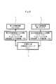
- FIG. 1 is a block diagram schematically showing a first basic configuration example and an information transmission system of a combined inspection system according to an embodiment of the present invention.
- FIG. 2 is a block diagram schematically showing a second basic configuration example and information transmission system of the combined inspection system according to the embodiment of the present invention.
- FIG. 3 is a block diagram schematically showing a third basic configuration example and an information transmission system of the combined inspection system according to the embodiment of the present invention.
- FIG. 4 is a block diagram schematically showing a fourth basic configuration example and an information transmission system of the combined inspection system according to the embodiment of the present invention.
- FIG. 5 is a block diagram schematically showing a fifth basic configuration example and information transmission system of the combined inspection system according to the embodiment of the present invention.
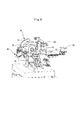
- FIG. 6 is a perspective view showing the overall structure of the first inspection apparatus according to the embodiment of the present invention.
- FIG. 7 is a front view of the first inspection apparatus shown in FIG.
- FIG. 8A is a side view schematically showing a configuration of an X-ray irradiation unit incorporated in the first inspection apparatus shown in FIG.
- FIG. 8B is a plan view of the same.
- FIG. 9 is a front view schematically showing another configuration example of the first inspection apparatus according to the embodiment of the present invention.
- FIG. 10 is a right side view schematically showing the configuration of the first inspection apparatus shown in FIG.
- FIG. 11 is a schematic diagram for explaining a measurement operation by the first inspection apparatus shown in FIG. FIG.
- FIG. 12A is a side view schematically showing the configuration of the X-ray irradiation unit incorporated in the first inspection apparatus shown in FIG.
- FIG. 12B is a plan view of the same.
- FIG. 13 is a block diagram showing a control system of the first inspection apparatus according to the embodiment of the present invention.
- FIG. 14 is a control flowchart of the first inspection apparatus according to the embodiment of the present invention.
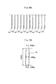
- FIG. 15A is a diagram showing parameters for analyzing the shape of the line and space pattern to be inspected.
- FIG. 15B is a diagram showing parameters for analyzing the shape of the line and space pattern created by the double exposure process.
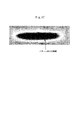
- FIG. 16A is a schematic cross-sectional view of a deep hole repeating structure to be inspected.
- FIG. 16A is a schematic cross-sectional view of a deep hole repeating structure to be inspected.
- FIG. 16B is an enlarged view of one deep hole in the schematic cross-sectional view shown in FIG. 16A.
- FIG. 17 is a diagram illustrating an example of measurement data obtained by a CD-SEM (second inspection apparatus).
- FIG. 18 is a diagram showing a usage example in which an observation image of a CD-SEM (second inspection apparatus) is fitted with a shape model of CD-SAXS (first inspection apparatus).
- FIGS. 1 to 5 are block diagrams schematically showing a basic configuration example and an information transmission system of a combined inspection system according to an embodiment of the present invention.
- the combined inspection system according to the present embodiment inspects a sample using a first inspection apparatus 1 that inspects the sample based on X-ray measurement data obtained by irradiating the sample with X-rays, and a measurement technique that does not use X-rays.
- the second inspection apparatus 2 is provided.
- the first inspection apparatus 1 for example, an X-ray nano shape measurement apparatus (CD-SAXS) is applied.
- the second inspection apparatus 2 for example, an optical inspection apparatus (OCD) or an inspection apparatus using a scanning electron microscope (CD-SEM) is applied.
- information from the first inspection apparatus 1 is output to the second inspection apparatus 2.
- information output from the first inspection apparatus 1 for example, in addition to measurement data obtained by X-ray measurement of a sample and the analysis result of the X-ray measurement data, information on the sample to be measured (Carrier, Wafer) Information).
- Carrier, Wafer information information on the sample to be measured.
- the OCD that constitutes the second inspection apparatus 2 uses light as a probe, it has advantages such as a small measurement area and a high throughput. Therefore, it is effective as an inspection device for in-line measurement in a semiconductor manufacturing process.
- OCD has a limit of resolution at a scale of 10 nm or less in pitch, and analysis becomes difficult as semiconductor elements are miniaturized.
- the CD-SAXS that constitutes the first inspection apparatus 1 is effective as an inspection apparatus that analyzes the nanometer-scale shape of the surface of the electronic device, and according to the configuration that includes an X-ray irradiation unit that will be described later, A small high-intensity X-ray source having a sufficiently powerful power for measuring a test pattern of 100 micrometers or less on the wafer surface can be obtained. Therefore, by using the information output from the first inspection apparatus 1, highly accurate analysis can be performed by the second inspection apparatus 2.
- Ethernet (Ethernet ⁇ registered trademark>) is used as a connection means
- any transmission method such as serial transmission such as RS-232C, optical transmission, or wireless transmission can be used.
- the first inspection device 1 and the second inspection device 2 are connected via the analysis server 3.
- the result of the first inspection device 1 is transmitted to the analysis server 3.
- the second inspection apparatus 2 obtains information from the analysis server 3.
- Ethernet registered trademark
- any transmission method such as serial transmission such as RS-232C, optical transmission, or wireless transmission can be used.
- the first inspection apparatus 1 and the second inspection apparatus 2 are connected via a host computer 4 (Host) that controls the process in a semiconductor factory.
- the result of the first inspection apparatus 1 is transmitted to the host computer 4 so that the second inspection apparatus 2 obtains information from the host computer 4.
- information is transmitted according to a standardized protocol called GEM300. If the host computer 4 is programmed, information transmission between the first and second inspection apparatuses 1 and 2 becomes possible.
- the first inspection device 1 and the second inspection device 2 are connected to the analysis server 3, and the analysis server 3 is further connected to the host computer 4. Yes.
- the analysis result of the first inspection device 1 and the measurement data of the second inspection device 2 are output to the analysis server 3, and the analysis server 3 outputs the analysis data from the second inspection device 2. Analysis of measurement data is executed. The analysis result is transmitted from the analysis server 3 to the host computer 4.
- information from the second inspection device 2 is output to the first inspection device 1.
- the first inspection apparatus 1 can perform highly accurate analysis.
- the first inspection device 1 and the second inspection device 2 are connected via a host computer 4 (Host) that controls the process in the semiconductor factory. Unlike the example, the result of the second inspection apparatus 2 is transmitted to the host computer 4. In a semiconductor manufacturing factory that normally uses a 300 mm wafer, information is transmitted according to a standardized protocol called GEM300. If the host computer 4 is programmed, information transmission between the first and second inspection apparatuses 1 and 2 becomes possible.
- OCD optical inspection apparatus
- the measurement / analysis procedure by OCD is as follows. First, prior to measurement, a large number of OCD-specific models into which parameters such as the detailed structure and material properties of the sample to be measured are input are created and stored as a library.
- a white light source is incident on the sample to be measured via a polarizer, light scattered by a fine pattern is detected by a spectroscope via an analyzer (spectral ellipsometer), and measurement
- a complex structure can be measured by combining several measurement techniques such as a method (reflectometer) in which light is incident directly above the target sample and the reflectance of the measurement target sample is measured.
- the spectrum waveform obtained by the measurement and the waveform calculated by the OCD model are compared, and the waveform waveform that most closely matches is determined as the shape of the measurement target sample. Based on this determination result, the shape is visualized and the dimensions of each part are output. The results obtained are fed back to model creation to improve analysis accuracy.
- OCD uses the analysis method as described above. Therefore, efficient measurement of dimensions is possible in the measurement range of the pattern that matches the model in the library, and it is applied as an in-line inspection of the semiconductor manufacturing process. Yes.
- OCD also has the following drawbacks. First, it takes a lot of time to create a library. In addition, it is necessary to prepare many actual samples for reference in order to create a library, which requires a lot of man-hours and costs.
- semiconductor miniaturization is progressing day by day, and if a fine pattern of 10 nm or less is measured, there is a limit of resolution coming from the wavelength range of incident light, and accurate dimension measurement becomes difficult.
- CD-SEM An inspection apparatus (CD-SEM) using a scanning electron microscope (SEM) is widely used in a semiconductor manufacturing line as a standard machine for measuring a two-dimensional dimension of a fine pattern in a semiconductor device.
- the measurement and analysis procedures using CD-SEM are as follows. That is, an SEM image is acquired for the measurement target sample, and the dimension of the measurement target sample is calculated from the image.
- the principle of image acquisition is the same as that of a normal SEM.
- An electron lens is used to focus an electron beam to a small diameter, scan the sample to be measured, and a secondary electron image and a reflected electron image emitted from the sample to be measured are obtained.
- An image is obtained by detection.
- the dimension calculation uses the contrast signal of the SEM image.
- the contrast distribution (line profile) of the location where the dimension is to be measured on the image is acquired, and the dimension of the measurement target sample is calculated from the line profile, the image magnification, and the number of pixels in the measurement section.
- CD-SEM has a merit that it has a deeper depth of focus than the optical type and can accurately measure the size of the bottom of the pattern.
- CD-SEM also has the following drawbacks. Depending on how the edge portion is taken from the line profile, the calculated dimension changes, so the reliability of the measurement result is low. Dimension measurement in the depth direction, where the electron beam may destroy the measurement target (especially organic matter such as resist), is not possible. Since CD-SEM has such drawbacks, there is a high possibility that it will not be able to cope with future semiconductor device manufacturing that will progress to further miniaturization and three-dimensionalization.
- FIG. 6 is a perspective view showing the entire structure of the first inspection apparatus
- FIG. 7 is a front view of the apparatus.
- the first inspection apparatus 1 includes an optical microscope 60 equipped with a sample stage 10, a positioning mechanism 20, a goniometer 30, an X-ray irradiation unit 40, an X-ray detector 50, a CCD camera, and the like.
- a semiconductor wafer (sample) to be inspected is disposed on the upper surface of the sample stage 10 and is driven by the positioning mechanism 20.
- the positioning mechanism 20 includes a horizontal movement mechanism that is movable in two perpendicular directions (X and Y directions) in a horizontal plane, a lifting mechanism that is movable in a vertical direction (Z direction) perpendicular to the horizontal plane, and an in-plane rotation mechanism.
- the sample stage 10 is moved in the X, Y, and Z directions and rotated in-plane so that an arbitrary measurement site on the semiconductor wafer disposed on the upper surface thereof is positioned in a predetermined direction to the irradiation X-ray convergence position. It has a function to do.
- the goniometer 30 includes first and second turning arms (turning members) 32 and 33 mounted on a goniometer body 31.
- the turning angle from the horizontal position of the first turning arm 32 is ⁇ S
- the turning angle from the horizontal position of the second turning arm 33 is ⁇ D
- the turning arms 32 and 33 are driven to turn.
- the first pivot arm 32 to pivot about the theta S axis, X-rays irradiation unit 40 are mounted. Further, the second pivot arm 33 to pivot about the theta D shaft are mounted the X-ray detector 50.
- the X-ray irradiation unit 40 has a function of condensing X-rays generated from the X-ray tube into characteristic X-rays having a specific wavelength and condensing them at one place.
- the position to which characteristic X-rays from the X-ray irradiation unit 40 are irradiated becomes the inspection position, and the measurement site of the sample arranged on the upper surface of the sample stage 10 is positioned to this inspection position by the positioning mechanism 20.
- the inspection position is set in the same plane as the surface of the sample placed on the sample stage 10.
- the X-ray detector 50 is used for X-ray reflectivity measurement (XRR) and small-angle X-ray scattering (SAXS) measurement.
- XRR X-ray reflectivity measurement
- SAXS small-angle X-ray scattering
- the film thickness and density are derived by measuring the interference between the reflected X-rays on the film surface and the reflected X-rays at the interface between the film and the substrate. Accuracy is obtained.
- the X-ray detector 50 for example, using a two-dimensional X-ray detector, X-ray reflectivity measurement in the TDI mode and small-angle X-ray scattering measurement in the Still mode can be performed.
- a measurement site of a sample (for example, a semiconductor wafer) arranged on the sample table 10 is arranged at a position below the optical microscope 60 by moving the sample table 10 by the positioning mechanism 20. Then, by moving in a horizontal direction from this position toward the inspection position, the measurement site of the sample (for example, a semiconductor wafer) is positioned at the inspection position.
- a sample for example, a semiconductor wafer
- FIG. 8A is a side view and FIG. 8B is a plan view.
- the X-ray irradiation unit 40 includes an X-ray tube 41, a first X-ray optical element 42, a second X-ray optical element 43, and a condensing slit 44.
- a condensing mirror having a multilayer film formed on the surface is used for the first and second X-ray optical elements 42 and 43.
- the unit body has a compact size and shape that can be mounted on the first swivel arm 32.
- the X-ray path will be described.
- the X-ray tube 41 an X-ray tube having an electron beam focal spot size on the target of ⁇ 100 ⁇ m or less, preferably 20 ⁇ m or less is used.
- the target material copper (Cu), molybdenum (Mo), silver (Ag), gold (Au), etc. can be selected, but small angle scattering having high angular resolution can be measured particularly when copper (Cu) is used. Is possible.
- X-rays emitted from the X-ray tube 41 first reach the first X-ray optical element 42. Then, the scattered X-ray 48 is condensed at the position of the X-ray detector 50 by the first X-ray optical element 42. As a result of focusing the scattered X-rays 48 on the X-ray detector 50 in this way, measurement with high angular resolution can be performed.
- the X-rays enter the second X-ray optical element 43, the light is collected in the vertical direction, and the incident X-rays 47 are collected on the surface of the sample 11. This also makes it possible to measure with high angular resolution when X-rays are grazingly incident on the surface of the sample 11 and X-ray reflectivity measurement or small-angle X-ray scattering measurement is performed.
- FIG. 9 is a front view schematically showing another configuration example of the first inspection apparatus, and FIG. 10 is a right side view of the same.
- the first inspection apparatus 1 shown in these drawings has a configuration suitable for a transmission-type small angle X-ray scattering apparatus (T-SAXS).
- the first inspection apparatus 1 shown in these drawings includes an optical microscope 60 equipped with a sample stage 10, a positioning mechanism 20, a goniometer 30, an X-ray irradiation unit 40, an X-ray detector 50, a CCD camera, and the like.
- the optical microscope 60 is omitted.
- a semiconductor wafer (sample) to be inspected is disposed on the upper surface of the sample stage 10 and is driven by the positioning mechanism 20.
- the positioning mechanism 20 includes a horizontal movement mechanism that is movable in two perpendicular directions (X and Y directions) in a horizontal plane, a lifting mechanism that is movable in a vertical direction (Z direction) perpendicular to the horizontal plane, and an in-plane rotation mechanism.
- the sample stage 10 is moved in the X, Y, and Z directions and rotated in-plane so that an arbitrary measurement site on the semiconductor wafer disposed on the upper surface thereof is positioned in a predetermined direction to the irradiation X-ray convergence position. It has a function to do.
- the goniometer 30 includes first and second turning arms (turning members) 32 and 33 mounted on a goniometer body 31.
- Each of the swivel arms 32 and 33 swivels around a virtual plane orthogonal to the upper surface of the sample table, with the axis ( ⁇ S axis, ⁇ D axis) perpendicular to the paper surface of FIG.
- the turning angle from the horizontal position of the first turning arm 32 is ⁇ S
- the turning angle from the horizontal position of the second turning arm 33 is ⁇ D
- the turning arms 32 and 33 are driven to turn.
- the first pivot arm 32 to pivot about the theta S axis, X-rays irradiation unit 40 are mounted. Further, the second pivot arm 33 to pivot about the theta D shaft are mounted the X-ray detector 50.
- the turning angle ⁇ S from the horizontal position of the first turning arm 32 can be driven to below the sample stage 10 (that is, ⁇ 90 °).
- transmission X-ray 49 as shown in FIG. 11 can be measured. Therefore, the first inspection apparatus 1 having such a configuration can be applied to a transmission-type small angle X-ray scattering apparatus (T-SAXS).
- T-SAXS transmission-type small angle X-ray scattering apparatus
- sample stage 10 and the positioning mechanism 20 need to transmit X-rays, they are formed of carbon, boron carbide, kapton, or the like having a small X-ray absorption coefficient, or as a cavity.
- FIG. 9 illustration of the positioning mechanism 20 and the support mechanism of the optical microscope 60 is omitted, but these support mechanisms are the swivel arms 32 and 33 of the goniometer, the X-ray irradiation unit 40, and the X-ray detector 50.
- the arrangement is such that it does not interfere with the surrounding components.
- FIG. 12A and 12B schematically show a configuration example of the X-ray irradiation unit 40 suitable when the first inspection apparatus 1 is configured by a transmission-type small angle X-ray scattering apparatus (T-SAXS).
- T-SAXS transmission-type small angle X-ray scattering apparatus
- the X-ray irradiation unit 40 shown in these drawings includes an X-ray tube 41, a first X-ray optical element 42, a second X-ray optical element 43, and a condensing slit 44 as constituent elements. .
- a condensing slit 44 as constituent elements.
- condensing mirrors having a multilayer film formed on the surface are used.
- These X-ray optical elements 42 and 43 have a structure enclosed in a housing not shown in order to prevent deterioration of the multilayer film.
- the housing has a mounting structure in which unnecessary stress is not applied so that the built-in X-ray optical elements 42 and 43 are not displaced or deformed.
- a position adjustment mechanism is provided so that high-precision alignment can be performed in each of the X-axis, Y-axis, and Z-axis directions.
- the X-ray tube 41 an X-ray tube having an electron beam focal spot size on the target of ⁇ 100 ⁇ m or less, preferably 20 ⁇ m or less is used.
- the target material copper (Cu), molybdenum (Mo), silver (Ag), gold (Au), etc. can be selected.
- Cu copper
- Mo molybdenum
- Au gold
- X-rays emitted from the X-ray tube 41 first reach the first X-ray optical element 42.
- the X-rays are collected in the horizontal direction (the direction parallel to the paper surface in FIG. 12B) by the first X-ray optical element 42 so that the position of the X-ray detector 50 is in focus.
- the light is condensed by the second X-ray optical element 43 in the vertical direction (in the direction parallel to the paper surface in FIG. 12A) so that the focus is similarly on the position of the X-ray detector 50.
- the condensed X-ray enters the measurement sample. X-rays are scattered by fine grooves and wirings formed in the measurement sample, pass through the sample, and reach the X-ray detector 50.
- a method of controlling the optical axis of the X-ray using the first and second X-ray optical elements 42 and 43 as described above is called a Kirkpatrick-Bayes method.
- the advantage of this method is that the two mirrors can be adjusted independently, so that the degree of freedom in controlling the shape of the focal point is high.
- this method although not shown, there is one in which two mirrors are integrated into an angle shape (L-shape), and this method may be used.
- This method of integrating two mirrors into an angle shape (L-shape) is called a side-by-side method, and it has advantages such as compactness of the optical system and easy alignment. Have.
- FIG. 13 is a block diagram showing a control system of the first inspection apparatus.
- the XG irradiation unit 40 is controlled by the XG controller 101.
- the sample image captured by the optical microscope 60 is recognized by the image recognition circuit 102.
- the optical microscope 60 and the image recognition circuit 102 constitute an image observation unit that observes an image of a sample placed on the sample stage 10. Note that the focus position of the optical microscope 60 is adjusted by the focus controller 103.
- the positioning controller 104 drives and controls the positioning mechanism 20 based on the sample image recognized by the optical microscope 60 and recognized by the image recognition circuit 102.
- the goniometer 30 is driven and controlled by the goniometer controller 106.
- the components of the XG controller 101, the image recognition circuit 102, the focus controller 103, the positioning controller 104, and the gonio controller 106 operate based on setting information sent from the central processing unit (CPU) 100, respectively.
- the setting information is stored in advance in the storage unit 110 as a recipe, and is read out by the central processing unit (CPU) 100 and output to the above-described components.
- the X-ray detector 50 is controlled by the count control circuit 107.
- the first inspection apparatus 1 also includes an operation unit 201 including a keyboard and a mouse for an operator to input various settings necessary for the operation of the apparatus. Further, the first inspection apparatus 1 includes a display unit 202 configured by a liquid crystal display or the like, and a communication unit 203 that executes data communication via a network.
- FIG. 14 is a flowchart showing an execution procedure of the X-ray thin film inspection method by the first inspection apparatus for inspecting a semiconductor wafer.
- Software for executing the X-ray thin film inspection is stored in the storage unit 110 in advance, and the central processing unit (CPU) 100 executes the following processing steps according to the software.
- the measurement site of the semiconductor wafer is positioned at the inspection position (step S1).
- unique points that can be specified by the image recognition circuit 102 based on image information from the optical microscope 60 are set in the storage unit 110 in advance as a recipe.
- the position information of the part to be measured is preset in the storage unit 110 as a recipe.
- a part that can be recognized by the image recognition circuit 102 without hesitation is set, such as a characteristic pattern shape formed on the surface of the semiconductor wafer.
- the image recognition circuit 102 recognizes and identifies the unique point set on the surface of the semiconductor wafer placed on the sample stage 10 from the image information from the optical microscope 60 based on the image information from the optical microscope 60.
- the positioning controller 104 drives and controls the positioning mechanism 20 based on the preset position information of the measurement site with the unique point recognized by the image recognition circuit 102 as a reference.
- the positioning mechanism 20 moves the sample table 10 in two horizontal directions (XY direction) and in the height direction (Z direction), and places the measured portion of the semiconductor wafer at the inspection position. If necessary, the semiconductor wafer is rotated in-plane by an in-plane rotation mechanism and arranged in a predetermined direction.
- step S2 X-ray inspection is executed (step S2), the central processing unit 100 analyzes the inspection data (step S3), and outputs the analysis result (step S2). S4).
- step S5 Each of the above steps is executed for all of the measurement sites set on the semiconductor wafer (step S5), and ends after the inspection of all the measurement sites is completed.
- GI-SAXS measurement method using the first inspection device a surface microstructure measurement method for measuring the microstructure on the sample surface when a reflective small-angle X-ray scattering device (GI-SAXS) is applied as the first inspection device 1 will be described.
- a sample is placed on a sample stage so that X-rays can enter from a direction orthogonal to the cross section to be measured.
- the measurement is performed by setting the line direction and the direction of incident X-rays in parallel.
- measurement is performed by arranging a sample so that a plurality of incident directions can be selected according to the in-plane symmetry.
- the X-ray incident angle with respect to the sample surface is set near the total reflection critical angle.
- the surface microstructure can be measured with high sensitivity.
- the X-ray diffraction pattern is recorded with a two-dimensional detector while rotating the sample in the plane.
- T-SAXS measurement method using the first inspection device Next, a surface microstructure measurement method for measuring the microstructure on the sample surface when a transmission type small angle X-ray scattering device (T-SAXS) is applied as the first inspection device 1 will be described.
- T-SAXS transmission type small angle X-ray scattering device
- the rotation angle range at that time is determined in consideration of the throughput and analysis accuracy. Here, if the sample is rotated in the cross-sectional direction of interest, data can be efficiently acquired with the minimum amount of rotation angle.
- a sample model is assumed based on parameters that specify the shape of the unit structure of the periodic structure of a predetermined sample, and the X-ray scattering intensity is calculated by simulation. That is, one or more layers are formed in the direction perpendicular to the surface due to the fine structure on the surface. In these layers, a sample model in which unit structures are periodically arranged in a direction parallel to the sample surface is assumed, and scattering of X-rays refracted and reflected by the respective interfaces is calculated. Based on the calculation result, the X-ray scattering intensity calculated by the sample model is fitted to the measured scattering intensity. Then, as a result of the fitting, the optimum value of the parameter that specifies the shape of the unit structure is determined.
- FIG. 15A is a diagram showing parameters for analyzing the shape of the line and space pattern to be inspected.
- lines 300 and spaces 301 are alternately and repeatedly formed.
- the height (Height), minimum line width (CD; CriticalCDimension), pitch (Pitch), side wall angle (Side-Wall Angle), top round (Top Round), bottom Defines round (Bottom Round).
- Arbitrary shapes can be expressed by combining geometric figures such as ellipses, straight lines, and curves according to the actual shape.
- FIG. 15B is a diagram showing parameters for analyzing the shape of the line and space pattern created by the double exposure process.
- the exposure is repeated a plurality of times. Further, a method for forming a fine structure of 10 nm or less by combining a method called self-alignment has been proposed.
- the first inspection apparatus 1 of the present invention it is possible to measure deviations of a plurality of photolithography processes in addition to a single pitch.
- FIG. 16A shows a schematic cross-sectional view of a deep hole repeating structure to be inspected.
- FIG. 16B is an enlarged view of one deep hole in the schematic cross-sectional view shown in FIG. 16A.
- the first inspection apparatus 1 can measure the hole diameter.
- FIG. 17 is a diagram illustrating an example of measurement data obtained by an inspection apparatus (CD-SEM) using a scanning electron microscope.
- an inspection apparatus CD-SEM
- a scanning electron microscope By using a CD-SEM as the second inspection apparatus 2, for example, an observation image of a pattern shape (measurement target) formed on a semiconductor substrate as shown in the figure can be obtained as measurement data.
- the OCD result is processed as an abnormal value due to disturbance. If the CD-SAXS value is also abnormal, it is processed as a shape abnormality.
- representative points may be measured in advance, or a procedure for measuring a target portion when an abnormality is found in OCD data may be used. In any case, the CD-SAXS data is used for the OCD inspection. By this method, it is possible to easily improve the inspection accuracy of OCD and identify the cause of abnormality.
- the CD-SEM calculates the CD by detecting the edge from the acquired line profile.
- the calculated dimension changes depending on how the edge portion is taken, there is a problem that the reliability of the measurement result is low. There is.
- a certain part of the target sample is measured by CD-SAXS.
- the same part is measured with a CD-SEM to obtain a line profile.
- the second inspection apparatus 2 includes the output value from the first inspection apparatus 1 (including the X-ray measurement data input from the first inspection apparatus 1 or the analysis result of the X-ray measurement data). It can also be used to verify the test results. That is, in the present invention configured to use an output value or the like from the first inspection device 1 in the second inspection device 2, the second inspection device 2 “inspects the sample” verifies the inspection result. It is a broad concept including operations (processes) such as performing.
- the contour position of the pattern shape formed on the semiconductor substrate to be measured can be estimated. Throughput can be improved.
- the first inspection apparatus 1 also uses the output value from the second inspection apparatus 2 (including the X-ray measurement data input from the second inspection apparatus 2 or the analysis result of the X-ray measurement data). Thus, the inspection result can be verified. That is, even in the present invention configured to use the output value from the second inspection apparatus 2 in the first inspection apparatus 1, “inspecting the sample” of the first inspection apparatus 1 This is a broad concept including operations (processes) such as verification.
Landscapes
- Chemical & Material Sciences (AREA)
- Biochemistry (AREA)
- Physics & Mathematics (AREA)
- Health & Medical Sciences (AREA)
- Life Sciences & Earth Sciences (AREA)
- Analytical Chemistry (AREA)
- Crystallography & Structural Chemistry (AREA)
- General Health & Medical Sciences (AREA)
- General Physics & Mathematics (AREA)
- Immunology (AREA)
- Pathology (AREA)
- Analysing Materials By The Use Of Radiation (AREA)
- Automobile Manufacture Line, Endless Track Vehicle, Trailer (AREA)
- Spectrometry And Color Measurement (AREA)
Abstract
Priority Applications (5)
| Application Number | Priority Date | Filing Date | Title |
|---|---|---|---|
| US16/205,832 US10983073B2 (en) | 2016-07-16 | 2017-07-14 | Hybrid inspection system |
| KR1020197003288A KR102232507B1 (ko) | 2016-07-16 | 2017-07-14 | 복합 검사 시스템 |
| JP2018528519A JP6942357B2 (ja) | 2016-07-16 | 2017-07-14 | 複合検査システム |
| CN201780042408.7A CN109416330B (zh) | 2016-07-16 | 2017-07-14 | 混合检查系统 |
| IL262449A IL262449B (en) | 2016-07-16 | 2018-10-17 | Hybrid inspection system |
Applications Claiming Priority (2)
| Application Number | Priority Date | Filing Date | Title |
|---|---|---|---|
| JP2016140944 | 2016-07-16 | ||
| JP2016-140944 | 2016-07-16 |
Publications (1)
| Publication Number | Publication Date |
|---|---|
| WO2018016430A1 true WO2018016430A1 (fr) | 2018-01-25 |
Family
ID=60992161
Family Applications (1)
| Application Number | Title | Priority Date | Filing Date |
|---|---|---|---|
| PCT/JP2017/025676 Ceased WO2018016430A1 (fr) | 2016-07-16 | 2017-07-14 | Système d'inspection combiné |
Country Status (7)
| Country | Link |
|---|---|
| US (1) | US10983073B2 (fr) |
| JP (1) | JP6942357B2 (fr) |
| KR (1) | KR102232507B1 (fr) |
| CN (1) | CN109416330B (fr) |
| IL (1) | IL262449B (fr) |
| TW (1) | TWI749029B (fr) |
| WO (1) | WO2018016430A1 (fr) |
Cited By (2)
| Publication number | Priority date | Publication date | Assignee | Title |
|---|---|---|---|---|
| JPWO2020194986A1 (fr) * | 2019-03-28 | 2020-10-01 | ||
| JP2024151218A (ja) * | 2023-04-11 | 2024-10-24 | トヨタ自動車株式会社 | データベース、サーバ、情報処理方法、及び情報処理プログラム |
Families Citing this family (7)
| Publication number | Priority date | Publication date | Assignee | Title |
|---|---|---|---|---|
| WO2020028412A1 (fr) * | 2018-07-31 | 2020-02-06 | Lam Research Corporation | Détermination d'un angle d'inclinaison dans des réseaux à motifs de structures à rapport d'aspect élevé |
| JP7458935B2 (ja) * | 2020-08-26 | 2024-04-01 | キオクシア株式会社 | 計測装置、及び、計測方法 |
| US11429091B2 (en) * | 2020-10-29 | 2022-08-30 | Kla Corporation | Method of manufacturing a semiconductor device and process control system for a semiconductor manufacturing assembly |
| KR20220170659A (ko) | 2021-06-23 | 2022-12-30 | 삼성전자주식회사 | 검사 장치 및 이를 이용한 검사 방법 |
| JP7600046B2 (ja) | 2021-07-13 | 2024-12-16 | キオクシア株式会社 | 形状計測方法、形状計測装置、及びプログラム |
| KR20230166404A (ko) | 2022-05-30 | 2023-12-07 | 삼성전자주식회사 | X-선 스캐터링을 이용한 반도체 소자 측정방법, 및 그 측정방법을 포함한 반도체 소자 제조방법 |
| CN121007513A (zh) * | 2024-11-08 | 2025-11-25 | 深圳中科飞测科技股份有限公司 | 一种应用于半导体关键尺寸量测的x射线量测系统 |
Citations (2)
| Publication number | Priority date | Publication date | Assignee | Title |
|---|---|---|---|---|
| JP2012237566A (ja) * | 2011-05-10 | 2012-12-06 | Hitachi High-Technologies Corp | 欠陥観察方法及びその装置 |
| WO2015066040A1 (fr) * | 2013-10-28 | 2015-05-07 | Kla-Tencor Corporation | Procédés et appareils de mesure d'alignement de dispositif à semi-conducteur faisant appel à la métrologie à rayons x |
Family Cites Families (23)
| Publication number | Priority date | Publication date | Assignee | Title |
|---|---|---|---|---|
| JPS5237186B2 (fr) | 1971-08-18 | 1977-09-20 | ||
| GB1432763A (en) | 1972-05-02 | 1976-04-22 | Dolby Laboratories Inc | Compressors expanders and noise reduction systems |
| US6891627B1 (en) * | 2000-09-20 | 2005-05-10 | Kla-Tencor Technologies Corp. | Methods and systems for determining a critical dimension and overlay of a specimen |
| FR2820822B1 (fr) * | 2001-02-14 | 2003-09-05 | Peugeot Citroen Automobiles Sa | Dispositif et procede de manipulation d'un produit et de traitement d'images radiocospiques du produit pour obtenir des coupes tomographiques et utilisations |
| JP5307503B2 (ja) * | 2008-07-01 | 2013-10-02 | 株式会社日立ハイテクサイエンス | X線分析装置及びx線分析方法 |
| DE112010001894B4 (de) | 2009-04-14 | 2023-05-04 | Rigaku Corp. | Verfahren zur Messung einer Oberflächenmikrostruktur, Verfahren zur Datenanalyse einer Oberflächenmikrostrukturmessung und Oberflächenmikrostruktur-Messsystem |
| JP5237186B2 (ja) | 2009-04-30 | 2013-07-17 | 株式会社リガク | X線散乱測定装置およびx線散乱測定方法 |
| WO2010147846A2 (fr) * | 2009-06-19 | 2010-12-23 | Kla-Tencor Technologies Corporation | Systèmes d'inspection et procédés pour détecter des défauts sur des ébauches de masque dans le domaine ultraviolet extrême |
| JP5367549B2 (ja) * | 2009-12-07 | 2013-12-11 | 株式会社東芝 | 基板計測方法 |
| JP5813923B2 (ja) * | 2010-03-15 | 2015-11-17 | 株式会社日立ハイテクサイエンス | X線透過検査装置及びx線透過検査方法 |
| JP2012154895A (ja) * | 2011-01-28 | 2012-08-16 | Hitachi High-Technologies Corp | 欠陥検査方法および欠陥検査装置 |
| US10801975B2 (en) * | 2012-05-08 | 2020-10-13 | Kla-Tencor Corporation | Metrology tool with combined X-ray and optical scatterometers |
| US20140067316A1 (en) * | 2012-08-30 | 2014-03-06 | Kabushiki Kaisha Toshiba | Measuring apparatus, detector deviation monitoring method and measuring method |
| KR102214643B1 (ko) * | 2013-07-08 | 2021-02-10 | 노바 메주어링 인스트루먼츠 엘티디. | 샘플 내 응력변형 분포 결정 방법 및 시스템 |
| GB201402318D0 (en) * | 2014-02-11 | 2014-03-26 | Oxford Instr Nanotechnology Tools Ltd | Method for materials analysis |
| WO2015146287A1 (fr) * | 2014-03-27 | 2015-10-01 | 株式会社リガク | Unité de génération de faisceau et dispositif de diffusion de rayons x à petit angle |
| JP6294130B2 (ja) * | 2014-04-04 | 2018-03-14 | 株式会社荏原製作所 | 検査装置 |
| US9640449B2 (en) * | 2014-04-21 | 2017-05-02 | Kla-Tencor Corporation | Automated inline inspection of wafer edge strain profiles using rapid photoreflectance spectroscopy |
| US9606073B2 (en) * | 2014-06-22 | 2017-03-28 | Bruker Jv Israel Ltd. | X-ray scatterometry apparatus |
| US10514345B2 (en) * | 2014-10-14 | 2019-12-24 | Rigaku Corporation | X-ray thin film inspection device |
| KR102144281B1 (ko) * | 2014-10-14 | 2020-08-13 | 가부시키가이샤 리가쿠 | X선 박막 검사 장치 |
| CN205015299U (zh) * | 2015-09-29 | 2016-02-03 | 王利晨 | X射线衍射装置 |
| US9916965B2 (en) * | 2015-12-31 | 2018-03-13 | Kla-Tencor Corp. | Hybrid inspectors |
-
2017
- 2017-07-14 WO PCT/JP2017/025676 patent/WO2018016430A1/fr not_active Ceased
- 2017-07-14 US US16/205,832 patent/US10983073B2/en active Active
- 2017-07-14 CN CN201780042408.7A patent/CN109416330B/zh active Active
- 2017-07-14 JP JP2018528519A patent/JP6942357B2/ja active Active
- 2017-07-14 KR KR1020197003288A patent/KR102232507B1/ko active Active
- 2017-07-14 TW TW106123661A patent/TWI749029B/zh active
-
2018
- 2018-10-17 IL IL262449A patent/IL262449B/en unknown
Patent Citations (2)
| Publication number | Priority date | Publication date | Assignee | Title |
|---|---|---|---|---|
| JP2012237566A (ja) * | 2011-05-10 | 2012-12-06 | Hitachi High-Technologies Corp | 欠陥観察方法及びその装置 |
| WO2015066040A1 (fr) * | 2013-10-28 | 2015-05-07 | Kla-Tencor Corporation | Procédés et appareils de mesure d'alignement de dispositif à semi-conducteur faisant appel à la métrologie à rayons x |
Cited By (13)
| Publication number | Priority date | Publication date | Assignee | Title |
|---|---|---|---|---|
| US11754515B2 (en) | 2019-03-28 | 2023-09-12 | Rigaku Corporation | Transmissive small-angle scattering device |
| WO2020194986A1 (fr) * | 2019-03-28 | 2020-10-01 | 株式会社リガク | Dispositif de diffusion à petit angle transmissif |
| KR20210144723A (ko) * | 2019-03-28 | 2021-11-30 | 가부시키가이샤 리가쿠 | 투과형 소각 산란 장치 |
| JP7210065B2 (ja) | 2019-03-28 | 2023-01-23 | 株式会社リガク | 透過型小角散乱装置 |
| JP2023033347A (ja) * | 2019-03-28 | 2023-03-10 | 株式会社リガク | 透過型小角散乱装置 |
| JP2023052136A (ja) * | 2019-03-28 | 2023-04-11 | 株式会社リガク | 透過型小角散乱装置 |
| JPWO2020194986A1 (fr) * | 2019-03-28 | 2020-10-01 | ||
| JP7401130B2 (ja) | 2019-03-28 | 2023-12-19 | 株式会社リガク | 透過型小角散乱装置 |
| JP7401131B2 (ja) | 2019-03-28 | 2023-12-19 | 株式会社リガク | 透過型小角散乱装置 |
| KR102650008B1 (ko) | 2019-03-28 | 2024-03-22 | 가부시키가이샤 리가쿠 | 투과형 소각 산란 장치 |
| US12019036B2 (en) | 2019-03-28 | 2024-06-25 | Rigaku Corporation | Transmissive small-angle scattering device |
| US12222303B2 (en) | 2019-03-28 | 2025-02-11 | Rigaku Corporation | Transmissive small-angle scattering device |
| JP2024151218A (ja) * | 2023-04-11 | 2024-10-24 | トヨタ自動車株式会社 | データベース、サーバ、情報処理方法、及び情報処理プログラム |
Also Published As
| Publication number | Publication date |
|---|---|
| CN109416330A (zh) | 2019-03-01 |
| TWI749029B (zh) | 2021-12-11 |
| US20190227006A1 (en) | 2019-07-25 |
| TW201809646A (zh) | 2018-03-16 |
| US10983073B2 (en) | 2021-04-20 |
| KR20190029627A (ko) | 2019-03-20 |
| JPWO2018016430A1 (ja) | 2019-04-25 |
| IL262449B (en) | 2022-06-01 |
| JP6942357B2 (ja) | 2021-09-29 |
| KR102232507B1 (ko) | 2021-03-26 |
| CN109416330B (zh) | 2022-09-27 |
| IL262449A (en) | 2019-03-31 |
Similar Documents
| Publication | Publication Date | Title |
|---|---|---|
| JP6942357B2 (ja) | 複合検査システム | |
| JP7001846B2 (ja) | X線計量方法 | |
| KR102550482B1 (ko) | X-선 산란계측을 이용한 깊은 구조체들에 대한 프로세스 모니터링 | |
| TWI739935B (zh) | 計量系統 | |
| JP7317849B2 (ja) | リアルタイム測定制御のための方法およびシステム | |
| TWI689702B (zh) | 用於高高寬比結構之x光散射測量計量 | |
| US10101671B2 (en) | Metrology methods, metrology apparatus and device manufacturing method | |
| KR102285100B1 (ko) | x선 기반 계측을 위한 측정 시스템 최적화 | |
| EP3548878B1 (fr) | Objectif zoom à rayons x pour diffusométrie de rayons x à petits angles | |
| CN113677983A (zh) | 结合x射线计量数据集合以改进参数评估的方法及系统 | |
| JP2020530942A (ja) | 目標物分解を使用したオンデバイス計測 | |
| KR20170139669A (ko) | 계산 효율적인 x 선 기반의 오버레이 측정 | |
| KR20230138482A (ko) | 왜곡된 형상을 갖는 심부 구조의 정확한 측정을 위한방법 및 시스템 | |
| TW201543003A (zh) | 以散射術量測為基礎之成像及關鍵尺寸度量 | |
| TW201350839A (zh) | 具有組合x光及光學散射計之計量工具 | |
| JP2007285923A (ja) | 反射モードのx線回折を用いた限界寸法の測定 | |
| JP6605276B2 (ja) | 計測装置、計測装置の校正方法および校正部材 |
Legal Events
| Date | Code | Title | Description |
|---|---|---|---|
| ENP | Entry into the national phase |
Ref document number: 2018528519 Country of ref document: JP Kind code of ref document: A |
|
| 121 | Ep: the epo has been informed by wipo that ep was designated in this application |
Ref document number: 17830949 Country of ref document: EP Kind code of ref document: A1 |
|
| NENP | Non-entry into the national phase |
Ref country code: DE |
|
| ENP | Entry into the national phase |
Ref document number: 20197003288 Country of ref document: KR Kind code of ref document: A |
|
| 122 | Ep: pct application non-entry in european phase |
Ref document number: 17830949 Country of ref document: EP Kind code of ref document: A1 |