WO2018043298A1 - Corps absorbant la lumière, bolomètre, corps absorbant les rayons infrarouges, dispositif de génération d'énergie thermique solaire, film de refroidissement rayonnant, et procédé de fabrication de corps absorbant la lumière - Google Patents
Corps absorbant la lumière, bolomètre, corps absorbant les rayons infrarouges, dispositif de génération d'énergie thermique solaire, film de refroidissement rayonnant, et procédé de fabrication de corps absorbant la lumière Download PDFInfo
- Publication number
- WO2018043298A1 WO2018043298A1 PCT/JP2017/030403 JP2017030403W WO2018043298A1 WO 2018043298 A1 WO2018043298 A1 WO 2018043298A1 JP 2017030403 W JP2017030403 W JP 2017030403W WO 2018043298 A1 WO2018043298 A1 WO 2018043298A1
- Authority
- WO
- WIPO (PCT)
- Prior art keywords
- dielectric
- thin film
- light absorber
- conductive thin
- light
- Prior art date
- Legal status (The legal status is an assumption and is not a legal conclusion. Google has not performed a legal analysis and makes no representation as to the accuracy of the status listed.)
- Ceased
Links
Images








Classifications
-
- G—PHYSICS
- G02—OPTICS
- G02B—OPTICAL ELEMENTS, SYSTEMS OR APPARATUS
- G02B5/00—Optical elements other than lenses
- G02B5/003—Light absorbing elements
-
- G—PHYSICS
- G01—MEASURING; TESTING
- G01J—MEASUREMENT OF INTENSITY, VELOCITY, SPECTRAL CONTENT, POLARISATION, PHASE OR PULSE CHARACTERISTICS OF INFRARED, VISIBLE OR ULTRAVIOLET LIGHT; COLORIMETRY; RADIATION PYROMETRY
- G01J1/00—Photometry, e.g. photographic exposure meter
- G01J1/02—Details
- G01J1/04—Optical or mechanical part supplementary adjustable parts
-
- G—PHYSICS
- G02—OPTICS
- G02B—OPTICAL ELEMENTS, SYSTEMS OR APPARATUS
- G02B5/00—Optical elements other than lenses
- G02B5/008—Surface plasmon devices
-
- G—PHYSICS
- G02—OPTICS
- G02B—OPTICAL ELEMENTS, SYSTEMS OR APPARATUS
- G02B5/00—Optical elements other than lenses
- G02B5/20—Filters
- G02B5/208—Filters for use with infrared or ultraviolet radiation, e.g. for separating visible light from infrared and/or ultraviolet radiation
-
- G—PHYSICS
- G02—OPTICS
- G02B—OPTICAL ELEMENTS, SYSTEMS OR APPARATUS
- G02B5/00—Optical elements other than lenses
- G02B5/20—Filters
- G02B5/22—Absorbing filters
-
- B—PERFORMING OPERATIONS; TRANSPORTING
- B82—NANOTECHNOLOGY
- B82Y—SPECIFIC USES OR APPLICATIONS OF NANOSTRUCTURES; MEASUREMENT OR ANALYSIS OF NANOSTRUCTURES; MANUFACTURE OR TREATMENT OF NANOSTRUCTURES
- B82Y20/00—Nanooptics, e.g. quantum optics or photonic crystals
Definitions
- the present invention relates to a light absorber, a bolometer, an infrared absorber, a solar thermal power generation device, a radiation cooling film, and a method for manufacturing the light absorber. More specifically, the present invention relates to a light absorber, a bolometer, an infrared absorber, a solar power generation device, a radiation cooling film, and a light absorber manufacturing method using surface plasmons.
- light absorber In the electromagnetic wave in the wavelength range (hereinafter referred to as “light” or “light wave”) handled in the optical field centering on visible light and infrared light, absorption is utilized for various applications. If you can design an object that absorbs light (“light absorber”) that shows good light absorption characteristics in a wide wavelength range or adjusts the value of the absorption rate for each wavelength, it can be used in a wide range of applications. Applicable and extremely useful. For example, for a thermal detection device such as a bolometer, a light absorber that replaces the current absorbing material such as gold black is required. In a solar cell, if the active layer can absorb light in a wide wavelength range of 300 nm to 2500 nm of sunlight, a great improvement in performance can be expected.
- a heat ray absorbing glass that absorbs sunlight in the infrared region has both a light transmission function and a heat ray shielding function, and can save energy such as cooling while having a normal glass function such as visible light transmission.
- Absorbers with high absorptance in the wavelength band that is the window region of the atmosphere are radiators of radiation cooling devices that efficiently release thermal energy into outer space from Kirchhoff's law where the absorptivity and emissivity are the same. Also useful. If such a good absorption characteristic can be realized in a wide wavelength region, and the wavelength region can be artificially adjusted, application in a wide variety of applications can be expected.
- Typical examples of light absorbers are pigments and dyes, which absorb light of a specific wavelength by utilizing the difference between the energy level of electrons and the vibration energy level of bonds. For this reason, in order to set the absorption wavelength range to a desired range, it is necessary to design a substance that exhibits absorption in a wavelength range depending on the chemical structure. In many cases, it is difficult to design pigments and dyes so that absorption is strengthened in one wavelength range and absorption is suppressed in another wavelength range to make it transparent, for example. In addition, pigments and dyes may cause problems in durability during long-term use.
- the absorption by surface plasmons can be adjusted by the design of the structure for supporting surface plasmons, and high durability can be expected. These properties are also important for application. For example, if absorption by surface plasmons is incorporated into an organic solar cell, a wide wavelength range can be used for power generation, and improvement in efficiency can be expected (plasmonic solar cell). As described above, when a plasmonic electrode having a plasmonic structure that supports surface plasmons is used instead of the transparent electrode that normally employs ITO in a solar cell, light absorption is enhanced by the supported surface plasmons, and photoelectric conversion is performed. Efficiency is improved. In addition, if an appropriate electrode structure is used, the enhanced light absorption exhibits almost no incident angle dependency or polarization dependency.
- Non-Patent Document 1 K. Aydin et al., Nat. Commun. 2, 517 (2011)
- Non-Patent Document 2 M. K. Hedayati et al., Adv. Mater. 23, 5410 (2011)
- a light absorber having an sandwiched MIM structure is disclosed.
- Non-Patent Document 3 (C. Ng et al., ACS Nano 10, 4704 (2016)) shows a MIM structure in which a transparent dielectric is sandwiched between a layer formed by aggregating gold nanoparticles and a thick flat gold thin film. A light absorber is disclosed.
- Non-Patent Document 1 discloses a light absorber having a metal-dielectric-metal (MIM) structure, but its absorption band is limited to 400 nm to 750 nm.
- MIM metal-dielectric-metal
- Non-Patent Document 2 discloses a light absorber having an MIM structure. Although the absorption rate is very high in the visible region, the absorption rate falls to 50% or less at 1000 nm.
- the light absorber of Non-Patent Document 3 discloses a light absorber having a MIM structure using particles. As far as the absorption rate of 350 nm to 1300 nm shown there is seen, it is 10% or less at 1300 nm in the near infrared region.
- the present invention contributes to the improvement of the performance of various products based on the principle of light absorption by developing the technology of the light absorber by providing a light absorber capable of exhibiting good absorption characteristics.
- the present inventor paid attention to a unique surface plasmon dispersion curve indicated by the MIM structure in the above-described method for improving the absorption performance by the MIM structure. Then, the present inventors completed the present invention by realizing that it is possible to achieve both high absorptivity and artificial manufacturability of the band by introducing a fine structure improved into the MIM structure to cause diffraction.
- a group of dielectric protrusions in which each dielectric protrusion protrudes from the dielectric surface at random positions along a certain dielectric surface, and each dielectric included in the group Conductive thin film disposed on or above at least part of the surface of the convex part and above or above at least part of the part of the dielectric surface where the dielectric convex part does not exist And a conductive thick film that extends away from the conductive thin film and extends along the dielectric surface.
- the dielectric convex portion in such a light absorber refers to a dielectric structure having a convex shape with at least a certain surface shape.
- the dielectric convex portion can be produced by various methods, and can be produced by an imprint technique (for example, nanoimprint) that molds a certain shape, a method using self-organization or phase separation, or the like.
- a conductive thin film is disposed in direct contact with at least a part of the surface of the dielectric convex portion and a portion of the dielectric surface where the dielectric convex portion does not exist, or via some kind of inclusion or intervening layer.
- the conductive thin film here is a film of a substance that exhibits at least some degree of conductivity in at least a certain frequency range.
- Such conductivity may be described in the present specification by the expression of metallic behavior.
- the thin film and the thick film in the conductive thin film and the conductive thick film are distinguished from each other by a thin film that uses at least a slight amount of energy transmission to light (including energy transfer by surface plasmons excited thereby).
- a film that does not expect to use transmitted light is called a thick film.
- a thick film does not mean a bulk material, and the thickness of the conductive thick film may be thinner than that of the conductive thin film.
- the term “thin film” and “thick film” are terms for distinction based only on optical transparency.
- the present invention can also be implemented by a method for manufacturing a light absorber. That is, in one aspect of the present invention, a step of forming a group of dielectric protrusions in which each dielectric protrusion protrudes from the dielectric surface at random positions along a certain dielectric surface, and included in the group Conductive thin film on or above at least a part of the surface of each dielectric protrusion and on or above at least a part of the dielectric surface where no dielectric protrusion exists. And a step of forming a conductive thick film extending away from the conductive thin film and extending along the dielectric surface is provided.
- light or light wave generally refers to electromagnetic waves in the wavelength region handled in the optical field, and particularly includes the ultraviolet, visible, near infrared, mid-infrared, and terahertz regions. Random means that the arrangement is disturbed to the extent that the regularity is broken.
- any aspect of the present invention it is possible to provide an absorber having a wider absorption band, adjustable wavelength range, and low incident angle dependency.
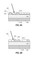
- FIG. 10A is an AFM image observed in the middle of manufacturing a light absorber sample for an example of the present invention, immediately after the formation of the conductive thin film 204 on the dielectric particles 202 (FIG. 10A), and the dielectric embedding It is the stage immediately after forming the layer 206 (FIG. 10B).
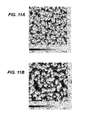
- FIGS. 11A and 11B are AFM images produced by changing the concentration of the particle dispersion for forming the dielectric particles 202 in the examples of the present invention, and having a particle dispersion concentration of 100% (FIG. 11A) and 10% (FIG. 11B).
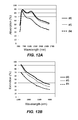
- Example of this invention it is a graph of the absorptivity spectrum (FIG. 12A) and extinction rate spectrum (FIG. 12B) of the light absorber sample produced by changing the density
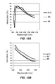
- the absorption spectrum (FIG. 15A) and the extinction coefficient spectrum (FIG. 15B) of a light absorber sample in which silver is used for the conductive thin film 204 and the thickness of the dielectric buried layer 206 is changed. It is a graph of.
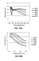
- the absorption spectrum (FIG. 16A) and the extinction ratio spectrum (FIG. 16A) of a light absorber sample in which gold is used for the conductive thin film 204 and the thickness of the dielectric buried layer 206 is changed. It is a graph of FIG. 16B).
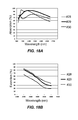
- FIG. 18 is a graph of the absorption spectrum of the light absorber sample by changing the incident angle ⁇ in the example of the embodiment of the present invention, and the incident angle ⁇ is set to 5 °, 30 °, and 70 ° in the order of FIGS. Is the case. It is a graph which shows the experimental result which confirmed that absorption in a wide band was realizable in the example in the embodiment of the present invention irrespective of the kind of conductive thin film, and made conductive thin film and conductive thickness into gold, aluminum, and silver. It is a graph of the absorptivity spectrum (FIG. 18A) and extinction rate spectrum (FIG.
- the light absorber realized in the present embodiment when properly designed, has a high absorptance in a wide wavelength range, which is dramatically different from absorption in a wavelength range of the conventional visible region and the near infrared region that is very close to the visible region.
- a high absorptance in a wide wavelength range which is dramatically different from absorption in a wavelength range of the conventional visible region and the near infrared region that is very close to the visible region.
- an absorption band extending from 400 nm to 5000 nm can be realized by designing mainly to widen the wavelength range.
- it is easy to artificially adjust the absorption band for example, to show sufficient transmittance in visible light and to have sufficient absorption in the infrared region.
- the absorption characteristics of the light absorber of the present embodiment also show a property that hardly depends on the incident angle.
- the principle of the absorber having such a high ability and the design concept thereof will be described, and a sample of the light absorber that has actually confirmed the principle
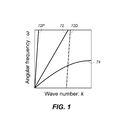
- FIG. 1 is an explanatory diagram showing the dispersion relationship between surface plasmons and light waves on a flat metal surface, and shows incident light (straight line 72) and surface plasmons (curve 74) when light is incident on a flat metal surface. Each dispersion relation is shown.
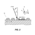
- FIG. 2 is a schematic sectional view showing a schematic configuration of a conventional absorber 70 in which a diffraction grating is formed on a metal surface to excite surface plasmons.
- the diffraction grating When a diffraction grating is present, the diffraction grating produces light in an inclined direction (for example, first-order diffracted light) that interferes with light from incident light (for example, incident light that is slightly inclined from the vertical).
- incident light for example, incident light that is slightly inclined from the vertical.
- the electric field of the diffracted light has a strong vertical component with respect to the metal surface (a plane extending in the left-right direction on the paper surface of FIG. 2).
- the problem of the incident light is the wave number component that travels parallel to the metal surface that can be coupled to the surface plasmon in the incident light. (Line 72P in FIG. 1).
- a straight line 72P represents the dispersion relation of the in-plane wave number (component parallel to the surface of the wave vector) of the incident light.
- the wave number k P of the surface plasmon coincides with the in-plane wave number (component parallel to the metal surface) k // of the incident light wave vector plus the lattice vector k G as shown in FIG. Then absorption occurs.
- FIG. 2 the wave number k P of the surface plasmon
- the straight line 72D provides an intersection where the momentum conservation law and the energy conservation law are established at the same time with respect to the curve 74 of the surface plasmon dispersion relation, so that energy transfer from light to the surface plasmon is allowed. . That is, if a diffraction grating exists, there is a possibility that surface plasmons are excited. The excited surface plasmon propagates on the metal surface and is absorbed by the metal as it propagates. This is the principle that the conventional absorber 70 having a diffraction grating gives light absorption.
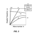
- FIG. 3 is an explanatory diagram showing the dispersion relationship of the conventional absorber 80 having the MIM structure in a graph, and the structure of the absorber 80 having the MIM structure is also added.
- the MIM structure absorber 80 provides a specific surface plasmon dispersion curve. More specifically, the curves 82 and 84 are multiplexed, and a curve 86 as another branch is also generated on the high frequency side. It should be noted that some of the curves 82 to 86 cross the straight line 72 or the straight line 72P, which is the dispersion relation of the incident light.
- the present invention proposes a new light absorber structure that expands the absorption band by incorporating randomness into the MIM structure.
- the dielectric convex portions randomly arranged in the plane along the dielectric surface are provided, and the portion of the dielectric surface where the dielectric convex portion does not exist above or above each dielectric convex portion.
- a light absorber is proposed in which a conductive thin film made of metal or the like is disposed on or above it.
- FIG. 4 is a schematic diagram showing a schematic configuration of the light absorber 100.
- FIG. 5 is an explanatory diagram showing a dispersion relation of in-plane wave numbers of diffracted light generated by dielectric particles randomly arranged in the plane.
- the light absorber 100 shown in FIG. 4 includes a group of dielectric convex portions 102, a conductive thin film 104, and a conductive thick film 108. Furthermore, the typical configuration of the light absorber 100 also includes a dielectric buried layer 106.
- the conductive thin film 104 is disposed on at least a part of the surface of each dielectric protrusion 102. Most typically, the conductive thin film 104 is formed in direct contact with the surface of each dielectric protrusion 102.
- the light to be absorbed is made incident from below on the paper surface on the side of the conductive thin film 104 in relation to the conductive thin film 104 and the conductive thick film 108 as shown by the thick solid arrow in FIG.
- FIG. Lines 12P and 12D1 in FIG. 5 indicate the dispersion relationship between the in-plane wave numbers of incident light and diffracted light when a one-dimensional diffraction grating as shown in FIG. 2 is adopted as the dielectric convex portion.
- Adopting dielectric particles as dielectric protrusions and making their positions random in the plane is equivalent to making the diffraction grating two-dimensional and breaking its regularity, and is caused by constructive interference.
- a width occurs in the direction of the diffracted light (diffraction angle), that is, a width is generated in the grating vector.
- the straight line 12D1 has a width according to the disorder of regularity, and the wave number itself of the diffracted light is broadened. Due to the randomness, a wave width of ⁇ k 1 (appended to the upper end of the graph) is generated in the wave number of diffracted light, and a width is generated at the intersections with the surface plasmon dispersion curves 22 to 26. Correspondingly, ⁇ 1 and ⁇ 2 are spread in a band for absorption, and absorption in a wide band can be expected.
- the conductive thin film 104 reflecting the shape of the dielectric convex portion 102 does not necessarily affect only the direction of the diffracted light.
- the surface plasmon dispersion curves 22 to 26 are similar to the dispersion curves 82 to 86 in FIG. 3 in FIG. 5 and the explanation based thereon, the dispersion of the surface plasmons is also influenced by the conductive thin film 104 reflecting the irregularities. receive.
- the distance to the conductive thick film 108 via the dielectric buried layer 106 has a width corresponding to the unevenness in each part of the conductive thin film 104.
- localized surface plasmons may occur due to the small size of the irregularities in the metal layer itself.
- the dispersion of the surface plasmon may have a width different from FIG.
- Such a width also has the effect of widening the band in the same manner as the wavenumber width of the diffracted light described above, and in any case, it can be said that it contributes to a wider band.
- the frequency range where the dispersion curve showing the relationship between the wave number (k) and the frequency ( ⁇ ) of the surface plasmon in the light absorber and the dispersion curve showing the relationship between the wave number and the frequency of the diffracted light are expanded. Therefore, it is possible to widen the absorption band using surface plasmons by forming a fine uneven shape having a particularly random arrangement on the metal surface.
- the light absorber 100 includes a group of dielectric protrusions 102, a conductive thin film 104, and a conductive thick film 108. Further, the typical structure of the light absorber 100 also includes a dielectric buried layer 106.
- the conductive thin film 104 is disposed on at least a part of the surface of each dielectric convex portion 102 and may cover the entire surface. In the most typical case, the conductive thin film 104 is formed in direct contact with the surface of each dielectric protrusion 102.
- a light absorber that functions in the same manner even when the conductive thin film 104 is disposed through another layer (not shown) that realizes a surface shape that is substantially a copy of the surface shape of each dielectric protrusion.
- the light absorber 100 is formed using a light-transmitting substrate such as the glass substrate 122.
- One surface 122A of the glass substrate 122 forms a dielectric surface on which the dielectric convex portion 102 is disposed. In the plane of the dielectric surface, the dielectric convex portions 102 are randomly located. This randomness gives a width to the dispersion relation of at least one of light and surface plasmon as described with reference to FIG. Note that the randomness introduced into the arrangement of the dielectric protrusions 102 in the light absorber 100 is appropriately determined according to the width of the necessary absorption band.
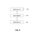
- FIG. 6 is a flowchart showing a method for manufacturing the light absorber.
- a group of dielectric convex portions 102 is formed (S02). This step includes forming a group of dielectric protrusions by any method. In that case, each dielectric convex part 102 which protrudes from the dielectric surface is arrange
- the conductive thin film 104 is disposed (S04).
- the conductive thin film 104 is formed on at least a part of the surface of each dielectric convex portion 102 included in the group of dielectric convex portions 102 or above and on one of the glass substrates 122 that is the dielectric surface.
- the surface 122A is disposed on or above at least a portion of the portion where the dielectric convex portion 102 does not exist.
- the conductive thick film 108 is formed (S06). The conductive thick film 108 is formed so as to spread along the dielectric surface at a position away from the conductive thin film 104.
- the most typical example of the light absorber 100 in this embodiment employs dielectric particles as in the light absorber 200 shown in FIG. 7A.
- dielectric particles 202 are employed as the dielectric protrusions 102 in the light absorber 100.
- the dielectric particles 202 are, for example, dielectric particles such as SiO 2 , and the particle size thereof is appropriately determined according to the purpose because it affects the absorption band as will be described later.
- the dielectric particles 202 are randomly arranged on one surface 222A of the glass substrate 222. There is no particular limitation on the shape of the dielectric particles that can be employed.
- the conductive thin film 204 is disposed at least at least a part of the surface of the glass substrate surface 222 ⁇ / b> A that is a dielectric surface where particles are not disposed, and each dielectric particle among the surfaces of the dielectric particles 202. It is at least a part of a region (upward on the paper surface) facing away from the surface 222A that is a dielectric surface arranged as viewed from 202.
- FIG. 8 is a flowchart showing a method of manufacturing a light absorber when employing dielectric particles. This flowchart corresponds to the manufacturing method shown in FIG. 6 and is a case where dielectric particles are employed.
- dielectric particles are arranged (S12) for the step of forming dielectric protrusions (S02). At this time, the dielectric particles are randomly arranged in the surface in contact with the surface of the base (for example, the glass substrate 222 having the surface 222A, FIG. 7A) having a two-dimensional surface as the dielectric surface.
- the surface of the base for example, the glass substrate 222 having the surface 222A, FIG. 7A
- Various methods can be adopted for randomly arranging the dielectric particles.
- the method includes the steps of randomly placing each dielectric particle in a plane by bringing a dispersion of dielectric particles into contact with the substrate, followed by fixing to the surface of the substrate.
- the density (surface density) of the dielectric particles arranged at random positions can be determined by the concentration of the particle dispersion. For this reason, for example, it is also preferable to set a reference value for the absorption coefficient or extinction coefficient, which is an index for determining the absorption performance, and to determine the concentration of the dispersion to obtain the reference value to some extent. At that time, a light absorber having the intended absorption can be produced with good reproducibility by reflecting fluctuations in the experiment and using a dispersion having a concentration higher than the concentration.
- the dielectric particles 202 that can be used for this purpose are, for example, silica (SiO 2 ) particles and various plastic particles such as polystyrene latex.
- the substrate described above is not made of a single material but may be made of a material having some surface layer or a thin film.
- the conductive thin film 204 is disposed on or above at least a part of the region of the dielectric layer and on or above at least a part of the part of the dielectric surface where the dielectric particles 202 are not disposed. (S14).
- the step (S16) for forming the conductive thick film is the same in this case.
- the dielectric particles 202 shown in the light absorber 200 shown in FIG. 7A can adopt various types in addition to the silica described above, and the shape, particle size, particle size distribution, There are no particular restrictions on the manufacturing method in principle. In practical terms, the material of the dielectric particles 202 may affect the randomness of the arrangement and the adhesion to the substrate and the conductive thin film. In order to select the absorption band, the shape, particle size, and particle size distribution of the dielectric particles 202 are adjusted to be appropriate. In the present embodiment, the dielectric particles cause the conductive thin film to be uneven by at least the shape of the protrusion.
- the conductive thin film 204 may have a structure shown in the light absorber 200a shown in FIG. 7B as another typical example. That is, in the step (S14) in which the conductive thin film 204 is disposed, among the surfaces of the dielectric particles 202, the conductive thin film 204 is formed on the top portion 202A, but on the lower side and the side surface 202B toward the glass substrate 222 side. May have a structure in which the conductive thin film 204 is not formed. Even if it is such, it can become a light absorber of this embodiment. In this structure, the conductive thin film 204 formed on the surface of the dielectric particles 202 is discontinuous with the conductive thin film 204 formed on the surface 222A in the recess 202R.
- the conductive thin film 204 formed on the plurality of adjacent dielectric particles 202 is such that the conductive region of the conductive thin film 204 is the dielectric particle 202 except that the dielectric particles 202 are close enough to contact each other. Each may form an isolated island.
- the conductive regions of the conductive thin film 204 of each dielectric particle 202 are continuous with each other. Shaped conductor regions may be formed. For this reason, in the light absorber 200a shown in FIG. 7B, randomness is introduced into the position of the conductor region that has an island shape, and randomness is also introduced into the size of the conductor region. Even in such a structure, it is said that the conductive thin film 204 is disposed on at least a part of the upper surface of the paper, which is the region facing the side opposite to the surface 222A, of the surface of each dielectric particle 202. sell.
- the conductive thin films 104 and 204 and the conductive thick films 108 and 208 can be made of a material that exhibits at least some conductivity.
- the metal material is selected such that it shows some response to the frequency in the wavelength range that causes absorption and does not transmit completely.
- oxide semiconductors for example, have a property that behaves metallically with respect to infrared rays. Therefore, if it is desired to cause absorption in the infrared rays, oxide semiconductors can be similarly employed.
- an oxide semiconductor that does not exhibit a metallic behavior in the visible band and exhibits a metallic behavior in the infrared band is one suitable material.
- the plasma frequency of the material can be used. That is, it is possible to select a material having a plasma frequency lower than the frequency in the wavelength range to be transmitted, and to exhibit the absorption ability in a frequency range (long wavelength range) lower than the plasma frequency. It is easy to secure a sufficient absorption bandwidth by applying the configuration of this embodiment.
- oxide semiconductor materials examples include, for example, In 2 O 3 (indium oxide), ITO (tin-doped indium oxide), Sr x Y 1-x TiO 3 (yttrium-doped strontium titanate), SnO 2 : F (fluorine-doped tin oxide), ZnO: Al or ZnO: Ga (aluminum or gallium-doped zinc oxide), TiO 2 : Nb (niobium-doped titanium oxide), Cd 2 SnO 4 (cadmium tin oxide).
- An organic conductive material such as PEDOT: PSS (poly (3,4-ethylenedioxythiophene) polystyrene sulfonate) can also be used.
- each of the conductive thin film and the conductive thick film is typically determined as follows, taking the light absorber 200 as an example. First, if the conductive thin film 204 is too thin, surface plasmons are hardly excited in the wavelength region to be absorbed, and may not function. On the other hand, if it is too thick, the light is excessively reflected, which is not preferable.
- the conductive thin film 204 can have a thickness that exhibits semi-transparency such that light passes through the wavelength band to be absorbed to some extent.
- the conductive thick film 208 is preferably thick enough to prevent transmission in the wavelength region to be absorbed. It is preferred that the thickness be sufficient to prevent the loss of absorption due to transmission.
- the thickness may be such that it reflects in the wavelength region.
- the transparency in the wavelength range to be transmitted is also considered.
- the conductive thin film is affected by the optical properties due to the presence of the dielectric convex portions 102 and the dielectric particles 202. For this reason, the light transmission itself may be different from the case where the same thickness layer is formed on a flat surface. Furthermore, due to the effect of the shape of the dielectric protrusions 102 and the dielectric particles 202, the conductive thin film may have a large number of holes, interruptions, wrinkles and steps.
- the conductive thin films are formed by the dielectric embedded layers 106 and 206, respectively. 104 and 204 are covered. The conductive thick films 108 and 208 are formed on or above the other surface of the dielectric buried layers 106 and 206.
- the dielectric buried layers 106 and 206 are preferably made of a material that can make the shapes of the dielectric convex portions 102 and the dielectric particles 202 at least to some extent.
- the shapes of the convex portions of the dielectric convex portions 102 and the dielectric particles 202 are not reflected on the conductive thick films 108 and 208 as they are. However, even if irregularities remain on the interface between the dielectric convex portions 102 and the dielectric particles 202 of the conductive thick films 108 and 208, the conductive thick films 108 and 208 operate as an absorber, so that the dielectric buried layers 106 and 206 are completely formed. Smoothness is not required.
- FIG. 9 is a schematic diagram showing a configuration in which light is incident from the same side as the protruding direction of the dielectric convex portion in the embodiment of the present invention.
- the configuration in which the dielectric convex portion is provided (FIG. 4)
- a light absorber 300 shown in FIG. 9A includes a group of dielectric convex portions 302, a conductive thin film 304, and a conductive thick film 308. Furthermore, the typical configuration of the light absorber 300 also includes a dielectric film 312 serving as a base material, and the group of dielectric convex portions 302 is positioned on at least one surface 312A side. The dielectric convex portions 302 are randomly formed in the plane along the one surface 312A.
- the conductive thick film 308 is disposed on the other surface 312B side of the dielectric film 312.
- the conductive thin film 304 is disposed at least in part or all of the portion where the dielectric convex portion is not formed on one surface 312A of the dielectric film 312 serving as the base material, and the dielectric convex portion. 302 part or all of the surface of each.
- the conductive thin film 304 is formed in direct contact with the surface of each dielectric protrusion 302.
- the light to be absorbed in this structure is incident from above on the paper surface on the dielectric convex portion 102 side due to the relationship between the conductive thin film 304 and the conductive thick film 308.
- the typical configuration of the light absorber 400 also includes a dielectric film 412 serving as a base material, and a group of dielectric particles 402 is located on at least one surface 412A side. Dielectric particles 402 are randomly formed in the plane along one surface 412A thereof.
- the conductive thick film 408 is disposed on the other surface 412B side of the dielectric film 412.
- the conductive thin film 404 is disposed at least in part or all of the portion of the dielectric surface 412A where the dielectric particles 402 are not disposed, and each dielectric particle among the surfaces of the dielectric particles 402. This is a part or all of the side (above the paper) facing away from the surface 412A, which is the dielectric surface arranged as viewed from 402.
- the conductive thin film becomes the light incident side when viewed from the conductive thick film.
- the light incident direction is reversed for the conductive thin film, and the light incident direction is reversed in view of the shape of the dielectric convex portion and the dielectric sphere.
- the operation and characteristics of the conductive thin film itself do not cause a difference that cannot be adjusted to other conditions.
- any of the light absorbers 100, 200, 300, and 400 positions that are valleys between adjacent ones of the dielectric convex portions 102 or the dielectric particles 202 (referred to as concave portions 102R and 202R for convenience).
- the conductive thin films 104 and 204 are formed.
- the material forming the concave portions 102R and 202R is affected by the arrangement density of the actual dielectric convex portions 102 and dielectric particles 202. When the density of the arrangement is high, it is a recess formed between the adjacent dielectric protrusions 102. When the density of the arrangement is low, the surface 122A is formed. Such a difference affects the light diffraction and scattering characteristics, and also affects the characteristics of the excited surface plasmon, and thus affects the absorption characteristics.
- Optical distance between the conductive thin film and the conductive thick film The width of the absorption wavelength band as the light absorber is mainly determined by the convex portions having a random arrangement introduced by the dielectric convex portions 102 and the dielectric particles 202. (FIGS. 4 and 7).
- the optical distance between the conductive thin film and the conductive thick film affects the position in the wavelength or frequency of the absorption wavelength band in addition to the influence of the materials of the conductive thin film and the conductive thick film described above. This optical distance can be easily set depending on the formation conditions of the dielectric buried layer when the dielectric buried layer is employed. In the configuration using the dielectric film shown in FIG. 9, it can be set by the thickness of the dielectric film.
- the center of the absorption wavelength is shifted to the long wavelength side, and when it is small, the center is shifted to the short wavelength side.
- the height of the dielectric protrusions and the particle size of the dielectric particles may also affect.
- a PET (polyethylene terephthalate) film having a thickness of about 1 ⁇ m or more in the infrared region can be employed.
- the light absorber of the present embodiment can be an absorber for a bolometer used as a power meter in the infrared or longer terahertz wave region.
- Preferred properties as a bolometer are sufficient sensitivity, less direction dependency of electromagnetic waves, and less change with time. Conventionally, gold black or the like is used.
- the light absorber of this embodiment can satisfy these properties.
- the performance (absorption band, etc.) of an absorber exhibiting good characteristics in the infrared region typified by the bolometer described above is determined according to the characteristics of a material such as gold black. For this reason, it is not easy to design an absorption band for a fixed application, such as a material having an absorption band matched to the atmospheric window.
- the absorber of this embodiment is suitable for such an application because the absorption band can be designed with a high degree of freedom.
- a solar thermal power generation device uses light in the entire spectral region of sunlight as a heat source.
- the light absorber of this embodiment it is possible to absorb all the energy of the entire spectrum region (0.3 ⁇ m to 2.5 ⁇ m) of sunlight, and a highly efficient light absorber can be manufactured. For this reason, what is suitable as a light absorber (photothermal converter) for solar thermal power generation can be provided by this embodiment.
- Sample Production Procedure A sample for the light absorber 200 using the dielectric particles of the above-described embodiment was produced. Taking the production of Sample 2 as an example, a 38.1 ⁇ 25.4 mm 2 glass substrate 222 (FIG. 7) is immersed in an aqueous solution of 1% volume ratio of aminopropyltrimethoxysilane for at least 1 minute, pulled up, and then watered. I did a rinse. Thereafter, baking was performed in an oven at 50 ° C. for 10 minutes.
- a glass substrate on which aminopropyltrimethoxysilane is fixed is dispersed in a 5% mass ratio of SiO 2 particles having a predetermined particle size (sample nominal value of 100 nm in sample 2) (colloidal silica microspheres, Polysciences, Inc.). Was immersed for at least 1 minute, pulled up and rinsed with water. Then, it baked for 10 minutes in 50 degreeC oven. Further, an MIM structure was formed by the following method. First, a silver thin film was deposited by a vacuum vapor deposition method under a condition that if the conductive thin film 204 was formed on a smooth surface as a conductive thin film 204 on the fixed dielectric particles 202, the film thickness should be 20 nm.
- This vapor deposition was performed at a deposition rate of 0.1 nm / s by resistance heating at a pressure of 5.0 ⁇ 10 ⁇ 4 Pa or less using a silver wire as a vapor deposition source. Thereafter, PMMA having a mass ratio of 3% in cellosolve acetate was deposited by spin coating as dielectric embedded layer 206. Usually, the film thickness is such that the light absorption effect of the present invention is obtained at 500 to 5000 rpm. Finally, a silver thin film with a thickness of 100 nm to be the conductive thick film 208 was formed by vacuum deposition.
- the conditions of the samples were changed in various ways in order to specify the relationship between the light wave absorption rate and the production conditions. Specifically, the particle diameter of the SiO 2 particles as the dielectric particles 202, the particle density of the particles, the film thickness of the conductive thin film 204, and the film thickness of the PMMA as the dielectric buried layer 206 (from the surface 222A) (Thickness) was changed. Table 1 lists the conditions of the prepared samples. For a sample different from sample 2, different conditions were adopted for the above-described manufacturing process depending on the changed conditions. Furthermore, in producing the sample of the light absorber 200 of the present embodiment, atomic force microscope (AFM) images were obtained at several stages and samples during the production.
- AFM atomic force microscope
- each column corresponds to the sample number, the particle diameter of the dielectric particle 202 (maker's nominal value), the dispersion concentration, the material of the conductive thin film 204, its thickness, the thickness of the PMMA of the dielectric buried layer 206, and so on.
- the concentration of the dispersion is a dilution ratio of the dispersion containing water having a mass ratio of 5% with water (reciprocal of the dilution ratio), and 100% means no dilution.
- the PMMA thickness of the dielectric buried layer 206 is a thickness from the surface 222A to the surface on which the conductive thick film 208 is formed, and the dielectric particles 202 and the conductive thin film 204 are embedded in the thickness range.
- the same kind of material as that of the conductive thin film 204 of the same sample was formed to a thickness sufficient to prevent transmission.
- FIG. 10 is an atomic force microscope (AFM) image in the middle of preparation of the sample 1 of the light absorber 200.
- AFM atomic force microscope
- particles having a diameter of 50 nm are formed at a dispersion concentration of 100%, and a 14.3 nm-thick aluminum layer is formed thereon as the conductive thin film 204 (FIG. 10A) and on the conductive thin film 204.
- FIG. 10B shows a stage where a PMMA layer (152 nm thickness) is formed as the dielectric buried layer 206. Note that the AFM image cannot be acquired by moving the particles only by fixing the particles, but is only after the aluminum is arranged.
- Table 2 summarizes the feature values measured from each AFM image, along with values on a surface (not shown) in which aluminum (thickness 14.3 nm) is directly formed on a glass substrate without placing particles.
- RMS root mean square roughness
- PMMA PMMA plays the role of the buried layer. This tendency was the same for other indices (average surface roughness Ra, maximum height difference between peak and valley).
- FIG. 11 is an AFM image obtained from Samples 2 and 3 prepared until the middle of the process for observation when the conditions are changed to change the particle density (FIGS. 11A and 11B in order).
- the particle size of the dielectric particles 202 is 100 nm
- the conductive thin film 204 is silver having a thickness of 20 nm.
- the AFM image cannot be obtained only with the particles before forming the conductive thin film 204, and becomes possible after forming the silver to be the conductive thin film 204. Therefore, the dielectric buried layer 206 is formed. Observed in the previous stage. As shown to FIG. 11A and B, it has confirmed that it was a structure where many dielectric particles 202 were arrange
- This extinction rate includes a decrease in light quantity due to scattering in addition to absorption.
- the wavelength range was 400 nm to 2500 nm for measurement UV / VIS, and 1250 nm to 4000 nm for FT-IR.
- sample 100 (FIG. 11A) with 100% of the particle dispersion has a clearly higher particle density than sample 3 (FIG. 11B) with the concentration of the particle dispersion of 10%.
- sample having the highest particle density was compared by changing the particle size to 100, 50, and 10 nm (FIG. 13).
- sample 12 having a particle diameter of 10 nm has a dispersion concentration of 50%, and the others are 100%.
- These samples showed no significant difference in the infrared region.
- the larger the particle size the higher the extinction rate.
- the extinction rate includes scattering, and the scattering intensity increases as the particle size increases. I don't think you can.
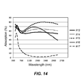
- the thickness of silver for the conductive thin film 204 was changed in the range of 10 nm to 50 nm in increments of 10 nm. Among these, 30 nm (sample 15) showed the maximum absorption in a wavelength region of 1000 nm or more. Furthermore, it was also observed that the absorptance decreased rapidly when the film thickness was 50 nm (sample 17). From this, in order to produce an absorber in a wavelength region of 1000 nm or more, for example, when silver is used as the material, it can be said that the upper limit of the thickness of the conductive thin film 204 is about 50 nm. Further, it was confirmed that the lower limit could be practical even at 10 nm in the investigated range.
- FIG. 17 is a graph of the extinction rate spectrum measured using the produced sample 20, and the incident angles ⁇ are 5 °, 30 °, and 70 ° in the order of FIGS. 17A to 17C. Although each spectrum is a separate graph, no substantial difference was found in its value, and it overlapped with a single curve on the drawing. Thereby, it was confirmed that the substantial angle dependence was not seen in the absorption rate in this embodiment. Further, regarding the dependence of the azimuth angle around the normal direction, all the light absorber samples obtained in this embodiment were isotropic (not shown). From these, it was confirmed that the light absorber sample of this embodiment does not show dependency on the incident angle.
- FIG. 18 is a graph showing the experimental results, in which gold, aluminum, and silver (samples 28, 29, and 30 in this order) are employed for the conductive thin film 204 and the conductive thick film 208, and the conductive thin film 204 and the dielectric buried layer.
- 19 is a graph of an absorptivity spectrum (FIG. 18A) and an extinction rate spectrum (FIG. 18B) of a light absorber sample in which the thickness of 206 is optimized.
- the incident angle ⁇ of the measurement is fixed at 8 °. As shown in FIG.
- 19 employs SiO 2 sphere particles having a diameter of 50 nm for the dielectric particles 202 and Au for the conductive thin film 204 and the conductive thick film 208.
- the thickness of the conductive thin film 204 is 12.2 nm. It is a SEM image which image
- the light absorber of the present embodiment exhibits a high absorption rate
- the absorption wavelength range can be designed, and the absorption characteristic does not exhibit incident angle dependency. confirmed.
- the performance of the light absorber can be further enhanced by various modifications, and more preferable characteristics can be realized depending on the application.
- the light absorber of the present embodiment includes a step of forming a group of dielectric convex portions in which each dielectric convex portion protrudes from the dielectric surface at random positions along a certain dielectric surface; A step of disposing a conductive thin film on or above at least a part of the surface of each dielectric convex portion included in the substrate, and a conductive thick film extending from the conductive thin film and extending along the dielectric surface. And a step of forming the light absorber.
- the light absorber can also be formed as a MIMIM structure, that is, a structure having three conductive layers. At that time, one or more conductive thin films having projections and depressions due to the influence of the dielectric protrusion are employed, and one conductive thick film is employed.
- the central conductive layer can be a conductive thick film, and the conductive layers on both sides of the conductive layer can be a conductive thin film having irregularities due to the influence of the dielectric convex portions.
- the light absorber having such a structure can have a desired absorption band on both sides. At that time, the absorption characteristics of each surface may be the same or may be changed.
- the light absorber of this embodiment can be used to improve performance in applications that can be used as a building material window by reducing the absorptivity in the visible light wavelength range (for example, a wavelength of 400 nm to 800 nm). It is possible to apply the disclosure of the above-described embodiment to design such that visible light has practical transmittance and the light (near-infrared) absorption rate is increased in the wavelength range of 800 nm to 2500 nm. . For this purpose, it is assumed that the oxide thin film is used for both the conductive thin film and the conductive thick film, and the absorption in the visible region of all materials located between them is suppressed.
- the conductive thick film has a thickness that does not transmit in the near-infrared region of 800 nm to 2500 nm, which increases the absorption rate. While measuring the absorption rate in that band, the thickness and material of the conductive thin film, the density of the dielectric protrusions The shape, the density and particle size of the dielectric particles, and the optical distance between the conductive thin film and the conductive thick film are adjusted. Thereby, the glass building material which has a desired heat ray prevention characteristic can be produced.
- Radiation Cooling Film If the ability to adjust the absorption rate according to the wavelength range of this embodiment is utilized, sunlight having a high absorption rate in the atmospheric window region with a wavelength of 8 ⁇ m to 13 ⁇ m and a wavelength of 0.3 ⁇ m to 2.5 ⁇ m It is possible to design a film with a high transmittance in the spectral region (“radiant cooling film”).
- This radiant cooling film can be realized, for example, by employing a polymer film for the dielectric film and using an oxide semiconductor for the conductive thin film and the conductive thick film. Since the emissivity and the absorptance are equal according to Kirchhoff's law, this radiant cooling film radiates heat into the outer space as infrared rays and gives a cooling effect.
- This radiant cooling film can be employed in any application where radiant cooling is useful.
- a radiant cooling film attached to the surface of a solar cell contributes to cooling of the solar cell. Since the photoelectric conversion efficiency increases as the temperature decreases in a silicon solar cell, improvement in power generation efficiency can be expected by attaching this radiation cooling film.
- another form similar to a radiant cooling film may be combined with reflection.
- high transmission as in solar cells is not always necessary for optical properties in the visible range. For example, if the reflectance is close to 100% in the visible range while achieving a high absorption rate in the above-described atmospheric window region, a radiation-cooling mirror that achieves both radiation cooling and reflection can be produced.
- a material having low absorption in the solar spectrum region such as silver or aluminum, is preferable.
- the light absorber of the present invention can be used for any device that utilizes light absorption.
Landscapes
- Physics & Mathematics (AREA)
- General Physics & Mathematics (AREA)
- Optics & Photonics (AREA)
- Health & Medical Sciences (AREA)
- Toxicology (AREA)
- Spectroscopy & Molecular Physics (AREA)
- Optical Filters (AREA)
- Optical Modulation, Optical Deflection, Nonlinear Optics, Optical Demodulation, Optical Logic Elements (AREA)
Abstract
Afin d'obtenir un corps absorbant la lumière dans lequel les longueurs d'onde absorbées peuvent être ajustées, un mode de réalisation de la présente invention concerne un corps d'absorption de lumière 100 pourvu d'un groupe de saillies diélectriques 102, d'un film mince conducteur 104, et d'un film épais conducteur 108. Le groupe de saillies diélectriques possédant chaque saillie diélectrique faisant saillie au niveau d'une position aléatoire sur une surface diélectrique. Un film mince diélectrique est disposé sur au moins une partie de la surface des saillies diélectriques ou au-dessus de celle-ci et sur au moins une partie de la surface diélectrique où les saillies diélectriques ne sont pas présentes ou au-dessus de celles-ci, et le film diélectrique épais s'étale le long de la surface diélectrique séparée du film mince diélectrique. Le groupe de saillies diélectriques peut être obtenu par disposition de particules diélectriques dans des positions aléatoires à l'intérieur de la surface. La présente invention concerne également un bolomètre, un corps absorbant les rayons infrarouges, un dispositif de génération d'énergie thermique solaire, et un film de refroidissement par rayonnement utilisant le corps absorbant la lumière ci-dessus, ainsi qu'un procédé de fabrication du corps absorbant la lumière.
Priority Applications (3)
| Application Number | Priority Date | Filing Date | Title |
|---|---|---|---|
| US16/329,134 US11802999B2 (en) | 2016-08-31 | 2017-08-24 | Light absorbing body, bolometer, infrared ray absorbing body, solar thermal power generating device, radiant cooling film, and method for manufacturing light absorbing body |
| JP2018537208A JP6877770B2 (ja) | 2016-08-31 | 2017-08-24 | 光吸収体、ボロメーター、赤外線吸収体、太陽熱発電装置、放射冷却フィルム、及び光吸収体の製造方法 |
| EP17846303.0A EP3508893B1 (fr) | 2016-08-31 | 2017-08-24 | Corps absorbant la lumière, bolomètre, corps absorbant les rayons infrarouges, dispositif de génération d'énergie thermique solaire, film de refroidissement rayonnant, et procédé de fabrication de corps absorbant la lumière |
Applications Claiming Priority (2)
| Application Number | Priority Date | Filing Date | Title |
|---|---|---|---|
| JP2016-169692 | 2016-08-31 | ||
| JP2016169692 | 2016-08-31 |
Publications (1)
| Publication Number | Publication Date |
|---|---|
| WO2018043298A1 true WO2018043298A1 (fr) | 2018-03-08 |
Family
ID=61301882
Family Applications (1)
| Application Number | Title | Priority Date | Filing Date |
|---|---|---|---|
| PCT/JP2017/030403 Ceased WO2018043298A1 (fr) | 2016-08-31 | 2017-08-24 | Corps absorbant la lumière, bolomètre, corps absorbant les rayons infrarouges, dispositif de génération d'énergie thermique solaire, film de refroidissement rayonnant, et procédé de fabrication de corps absorbant la lumière |
Country Status (4)
| Country | Link |
|---|---|
| US (1) | US11802999B2 (fr) |
| EP (1) | EP3508893B1 (fr) |
| JP (1) | JP6877770B2 (fr) |
| WO (1) | WO2018043298A1 (fr) |
Cited By (6)
| Publication number | Priority date | Publication date | Assignee | Title |
|---|---|---|---|---|
| CN109631416A (zh) * | 2019-01-04 | 2019-04-16 | 重庆大学 | 水气两用平板型太阳能集热和辐射制冷综合利用装置 |
| WO2020240366A1 (fr) * | 2019-05-31 | 2020-12-03 | 3M Innovative Properties Company | Film de refroidissement composite et article le comprenant |
| WO2021212538A1 (fr) * | 2020-04-20 | 2021-10-28 | 宁波瑞凌新能源科技有限公司 | Plaque métallique de réfrigération par rayonnement, son procédé de préparation et son application |
| WO2022097337A1 (fr) * | 2020-11-06 | 2022-05-12 | 国立大学法人大阪大学 | Dispositif de rayonnement, dispositif de refroidissement à rayonnement et procédé de fabrication de dispositif de rayonnement |
| US11833780B2 (en) | 2020-04-20 | 2023-12-05 | Ningbo Radi-Cool Advanced Energy Technologies Co., Ltd. | Radiative cooling metal plate, preparation method and application thereof |
| US11906252B2 (en) | 2019-05-31 | 2024-02-20 | 3M Innovative Properties Company | Composite cooling film and article including the same |
Families Citing this family (8)
| Publication number | Priority date | Publication date | Assignee | Title |
|---|---|---|---|---|
| WO2019029207A1 (fr) * | 2017-08-11 | 2019-02-14 | 中国科学院上海微系统与信息技术研究所 | Métamatériaux d'absorption électromagnétique |
| WO2020140082A1 (fr) | 2018-12-27 | 2020-07-02 | SkyCool Systems, Inc. | Système de panneau de refroidissement |
| CN113906261A (zh) | 2019-04-17 | 2022-01-07 | 天酷系统股份有限公司 | 辐射冷却系统 |
| CN112613173B (zh) * | 2020-12-18 | 2022-08-26 | 北京理工大学 | 一种金黑薄膜吸收率计算模拟方法 |
| CN115721762B (zh) * | 2021-09-01 | 2025-08-15 | 张明正 | 奈米结构光载体 |
| CN114543372B (zh) * | 2022-02-21 | 2023-11-17 | 中南大学 | 一种适用于宽温度范围的高性能太阳能光谱选择性吸热器 |
| JP2025028514A (ja) | 2023-08-18 | 2025-03-03 | 国立研究開発法人産業技術総合研究所 | 電磁波吸収体およびその製造方法 |
| CN117073242A (zh) * | 2023-08-25 | 2023-11-17 | 桂林电子科技大学 | 一种基于双层纳米圆盘阵列结构的全光谱太阳能吸收器 |
Citations (5)
| Publication number | Priority date | Publication date | Assignee | Title |
|---|---|---|---|---|
| JP2012014976A (ja) * | 2010-07-01 | 2012-01-19 | Canon Inc | 発光素子とその製造方法 |
| JP2012164980A (ja) * | 2011-01-21 | 2012-08-30 | Sumitomo Metal Mining Co Ltd | 光電変換装置とその製造方法 |
| JP2015010825A (ja) * | 2013-06-26 | 2015-01-19 | スタンレー電気株式会社 | 局在プラズモン共鳴チップ |
| WO2015011009A1 (fr) * | 2013-07-24 | 2015-01-29 | Eth Zurich | Absorbeur plasmonique à large bande et à couche mince |
| JP2015121417A (ja) * | 2013-12-20 | 2015-07-02 | 三菱電機株式会社 | 電磁波検出器 |
Family Cites Families (16)
| Publication number | Priority date | Publication date | Assignee | Title |
|---|---|---|---|---|
| US5403435A (en) * | 1992-01-23 | 1995-04-04 | Micron Technology, Inc. | Process for selectively etching integrated circuit devices having deep trenches or troughs or elevated features with re-entrant profiles |
| US6080987A (en) * | 1997-10-28 | 2000-06-27 | Raytheon Company | Infrared-sensitive conductive-polymer coating |
| JPWO2008018247A1 (ja) * | 2006-08-09 | 2009-12-24 | 日本板硝子株式会社 | 透過型偏光素子及びそれを用いた複合偏光板 |
| US8013238B2 (en) * | 2007-07-09 | 2011-09-06 | Energy Related Devices, Inc. | Micro concentrators elastically coupled with spherical photovoltaic cells |
| US9136422B1 (en) * | 2012-01-19 | 2015-09-15 | Alta Devices, Inc. | Texturing a layer in an optoelectronic device for improved angle randomization of light |
| FR2954856B1 (fr) * | 2009-12-30 | 2012-06-15 | Saint Gobain | Cellule photovoltaique organique et module comprenant une telle cellule |
| US20140154668A1 (en) * | 2010-05-21 | 2014-06-05 | The Trustees Of Princeton University | Structures for Enhancement of Local Electric Field, Light Absorption, Light Radiation, Material Detection and Methods for Making and Using of the Same. |
| US20160003744A1 (en) * | 2012-04-10 | 2016-01-07 | The Trustees Of Princeton University | Plasmonic Nanocavity Array Sensors for Analyte Detection Enhancement and Methods for Making and Using of the Same |
| US9348078B2 (en) * | 2010-06-08 | 2016-05-24 | Pacific Integrated Energy, Inc. | Optical antennas with enhanced fields and electron emission |
| EP2583317A4 (fr) * | 2010-06-18 | 2016-06-15 | Glo Ab | Structure à diodes électroluminescentes de nanofils et procédé de fabrication associé |
| EP2839540A4 (fr) | 2012-04-16 | 2015-12-16 | Univ Duke | Appareil et procédé de fourniture d'une structure à absorption sélective |
| JP6353845B2 (ja) * | 2012-10-26 | 2018-07-04 | グロ アーベーGlo Ab | ナノワイヤled構造の製造方法 |
| CA2899045A1 (fr) | 2013-02-21 | 2014-08-28 | The Governing Council Of The University Of Toronto | Dispositifs photovoltaiques comportant des nanoparticules plasmoniques |
| US20150036234A1 (en) | 2013-08-01 | 2015-02-05 | Board Of Regents, The University Of Texas System | Methods and compositions related to dielectric coated metal nanoparticles in thin-film opto-electronic conversion devices |
| FR3012363B1 (fr) * | 2013-10-30 | 2015-10-23 | Saint Gobain | Element en couches transparent |
| WO2016069083A2 (fr) * | 2014-09-09 | 2016-05-06 | The University Of North Carolina At Charlotte | Détecteur optique basé sur une surface diélectrique à structure antiréfléchissante et sur un absorbeur métallique |
-
2017
- 2017-08-24 WO PCT/JP2017/030403 patent/WO2018043298A1/fr not_active Ceased
- 2017-08-24 JP JP2018537208A patent/JP6877770B2/ja active Active
- 2017-08-24 US US16/329,134 patent/US11802999B2/en active Active
- 2017-08-24 EP EP17846303.0A patent/EP3508893B1/fr active Active
Patent Citations (5)
| Publication number | Priority date | Publication date | Assignee | Title |
|---|---|---|---|---|
| JP2012014976A (ja) * | 2010-07-01 | 2012-01-19 | Canon Inc | 発光素子とその製造方法 |
| JP2012164980A (ja) * | 2011-01-21 | 2012-08-30 | Sumitomo Metal Mining Co Ltd | 光電変換装置とその製造方法 |
| JP2015010825A (ja) * | 2013-06-26 | 2015-01-19 | スタンレー電気株式会社 | 局在プラズモン共鳴チップ |
| WO2015011009A1 (fr) * | 2013-07-24 | 2015-01-29 | Eth Zurich | Absorbeur plasmonique à large bande et à couche mince |
| JP2015121417A (ja) * | 2013-12-20 | 2015-07-02 | 三菱電機株式会社 | 電磁波検出器 |
Non-Patent Citations (9)
| Title |
|---|
| C. NG ET AL., ACS NANO, vol. 10, 2016, pages 4704 |
| C. NG ET AL.: "Hot Carrier Extraction with Plasmonic Broadband Absorbers", ACS NANO, vol. 10, no. 4, 16 March 2016 (2016-03-16), pages 4704 - 4711, XP055584909 * |
| C. NG ET AL.: "Hot Carrier Extraction with Plasmonic Broadband Absorbers", ACS NANO, vol. 10, no. 4, 2016, pages 4704 - 4711 |
| K. AYDIN ET AL., NAT. COMMUN., vol. 2, 2011, pages 517 |
| K. AYDIN ET AL.: "Broadband polarization- independent resonant light absorption using ultrathin plasmonic super absorbers", NATURE COMMUNICATIONS, vol. 2, no. 517, 1 November 2011 (2011-11-01), pages 1 - 7, XP055057355 * |
| K. AYDIN ET AL.: "Broadband polarization-independent resonant light absorption using ultrathin plasmonic super absorbers", NAT. COMMUN., vol. 2, 2011, pages 517, XP055057355, DOI: doi:10.1038/ncomms1528 |
| K. HEDAYATI ET AL.: "Design of a Perfect Black Absorber at Visible Frequencies Using Plasmonic Metamaterials", ADV. MATER., vol. 23, no. 45, 2011, pages 5410 - 5414 |
| M. K. HEDAYATI ET AL., ADV. MATER., vol. 23, 2011, pages 5410 |
| M. K. HEDAYATI ET AL.: "Design of a Perfect Black Absorber at Visible Frequencies Using Plasmonic Metamaterials", ADVANCED MATERIALS, vol. 23, no. 45, 14 October 2011 (2011-10-14), pages 5410 - 5414, XP055584905 * |
Cited By (9)
| Publication number | Priority date | Publication date | Assignee | Title |
|---|---|---|---|---|
| CN109631416A (zh) * | 2019-01-04 | 2019-04-16 | 重庆大学 | 水气两用平板型太阳能集热和辐射制冷综合利用装置 |
| WO2020240366A1 (fr) * | 2019-05-31 | 2020-12-03 | 3M Innovative Properties Company | Film de refroidissement composite et article le comprenant |
| CN113874213A (zh) * | 2019-05-31 | 2021-12-31 | 3M创新有限公司 | 复合冷却膜和包括该复合冷却膜的制品 |
| CN113874213B (zh) * | 2019-05-31 | 2022-07-01 | 3M创新有限公司 | 复合冷却膜和包括该复合冷却膜的制品 |
| US11906252B2 (en) | 2019-05-31 | 2024-02-20 | 3M Innovative Properties Company | Composite cooling film and article including the same |
| US12339471B2 (en) | 2019-05-31 | 2025-06-24 | 3M Innovative Properties Company | Composite cooling film and article including the same |
| WO2021212538A1 (fr) * | 2020-04-20 | 2021-10-28 | 宁波瑞凌新能源科技有限公司 | Plaque métallique de réfrigération par rayonnement, son procédé de préparation et son application |
| US11833780B2 (en) | 2020-04-20 | 2023-12-05 | Ningbo Radi-Cool Advanced Energy Technologies Co., Ltd. | Radiative cooling metal plate, preparation method and application thereof |
| WO2022097337A1 (fr) * | 2020-11-06 | 2022-05-12 | 国立大学法人大阪大学 | Dispositif de rayonnement, dispositif de refroidissement à rayonnement et procédé de fabrication de dispositif de rayonnement |
Also Published As
| Publication number | Publication date |
|---|---|
| JP6877770B2 (ja) | 2021-05-26 |
| US11802999B2 (en) | 2023-10-31 |
| US20190391301A1 (en) | 2019-12-26 |
| EP3508893A1 (fr) | 2019-07-10 |
| EP3508893B1 (fr) | 2023-01-11 |
| EP3508893A4 (fr) | 2020-05-13 |
| JPWO2018043298A1 (ja) | 2019-07-04 |
Similar Documents
| Publication | Publication Date | Title |
|---|---|---|
| JP6877770B2 (ja) | 光吸収体、ボロメーター、赤外線吸収体、太陽熱発電装置、放射冷却フィルム、及び光吸収体の製造方法 | |
| Yang et al. | Compact multilayer film structures for ultrabroadband, omnidirectional, and efficient absorption | |
| Catchpole et al. | Design principles for particle plasmon enhanced solar cells | |
| Bossard et al. | Near-ideal optical metamaterial absorbers with super-octave bandwidth | |
| JP7203431B2 (ja) | 電界効果調整可能イプシロンニアゼロ吸収装置 | |
| Hedayati et al. | The hybrid concept for realization of an ultra-thin plasmonic metamaterial antireflection coating and plasmonic rainbow | |
| Liu et al. | Ultrathin planar broadband absorber through effective medium design | |
| Zou et al. | Broadband mid-infrared perfect absorber using fractal Gosper curve | |
| CN110196464A (zh) | 一种实现超宽带光吸收的方法以及一种复合微结构 | |
| Yin et al. | Light absorption enhancement for ultra-thin Cu (In1− xGax) Se2 solar cells using closely packed 2-D SiO2 nanosphere arrays | |
| Sun et al. | Optimized broadband metamaterial absorber for solar photothermal conversion | |
| Ma et al. | High-efficiency and ultrabroadband flexible absorbers based on transversely symmetrical multi-layer structures | |
| CN112909565A (zh) | 一种混合图案化金属-石墨烯超表面的多波带吸收器 | |
| Qian et al. | A broadband and polarization-independent metasurface perfect absorber for hot-electron photoconversion | |
| Yang et al. | Light trapping enhancement in a thin film with 2D conformal periodic hexagonal arrays | |
| Matsui et al. | Assembled films of Sn-doped In2O3 plasmonic nanoparticles on high-permittivity substrates for thermal shielding | |
| Hakamada et al. | Carbon‐coated moth‐eye structure: An ultrabroadband THz‐DUV near‐perfect absorber | |
| CN110703371A (zh) | 半导体超表面电磁波吸收器及其制备方法 | |
| US10935707B1 (en) | Optical coating for spectral conversion | |
| Jin et al. | Ultrahigh omnidirectional, broadband, and polarization-independent optical absorption over the visible wavelengths by effective dispersion engineering | |
| Jalali | Impact of one-dimensional photonic crystal back reflector in thin-film c-Si solar cells on efficiency: Impact of one-dimensional photonic crystal | |
| Guillén et al. | Plasmonic characteristics of Ag and ITO/Ag ultrathin films as-grown by sputtering at room temperature and after heating | |
| CN113325495A (zh) | 一种基于三重米氏共振的超宽带超表面完美吸收器 | |
| Guo et al. | Impact of interface roughness on the performance of broadband blackbody absorber based on dielectric-metal film multilayers | |
| KR102955700B1 (ko) | 엡실론-근사-제로 물질의 제조 방법 |
Legal Events
| Date | Code | Title | Description |
|---|---|---|---|
| 121 | Ep: the epo has been informed by wipo that ep was designated in this application |
Ref document number: 17846303 Country of ref document: EP Kind code of ref document: A1 |
|
| ENP | Entry into the national phase |
Ref document number: 2018537208 Country of ref document: JP Kind code of ref document: A |
|
| NENP | Non-entry into the national phase |
Ref country code: DE |
|
| ENP | Entry into the national phase |
Ref document number: 2017846303 Country of ref document: EP Effective date: 20190401 |