WO2018047501A1 - 貼り合わせ用基板の表面欠陥の評価方法 - Google Patents
貼り合わせ用基板の表面欠陥の評価方法 Download PDFInfo
- Publication number
- WO2018047501A1 WO2018047501A1 PCT/JP2017/027102 JP2017027102W WO2018047501A1 WO 2018047501 A1 WO2018047501 A1 WO 2018047501A1 JP 2017027102 W JP2017027102 W JP 2017027102W WO 2018047501 A1 WO2018047501 A1 WO 2018047501A1
- Authority
- WO
- WIPO (PCT)
- Prior art keywords
- polycrystalline silicon
- silicon layer
- substrate
- defects
- bonding
- Prior art date
- Legal status (The legal status is an assumption and is not a legal conclusion. Google has not performed a legal analysis and makes no representation as to the accuracy of the status listed.)
- Ceased
Links
Images
Classifications
-
- H—ELECTRICITY
- H10—SEMICONDUCTOR DEVICES; ELECTRIC SOLID-STATE DEVICES NOT OTHERWISE PROVIDED FOR
- H10P—GENERIC PROCESSES OR APPARATUS FOR THE MANUFACTURE OR TREATMENT OF DEVICES COVERED BY CLASS H10
- H10P90/00—Preparation of wafers not covered by a single main group of this subclass, e.g. wafer reinforcement
- H10P90/19—Preparing inhomogeneous wafers
- H10P90/1904—Preparing vertically inhomogeneous wafers
- H10P90/1906—Preparing SOI wafers
- H10P90/1914—Preparing SOI wafers using bonding
-
- G—PHYSICS
- G01—MEASURING; TESTING
- G01N—INVESTIGATING OR ANALYSING MATERIALS BY DETERMINING THEIR CHEMICAL OR PHYSICAL PROPERTIES
- G01N21/00—Investigating or analysing materials by the use of optical means, i.e. using sub-millimetre waves, infrared, visible or ultraviolet light
- G01N21/84—Systems specially adapted for particular applications
- G01N21/88—Investigating the presence of flaws or contamination
- G01N21/95—Investigating the presence of flaws or contamination characterised by the material or shape of the object to be examined
- G01N21/956—Inspecting patterns on the surface of objects
-
- G—PHYSICS
- G01—MEASURING; TESTING
- G01N—INVESTIGATING OR ANALYSING MATERIALS BY DETERMINING THEIR CHEMICAL OR PHYSICAL PROPERTIES
- G01N1/00—Sampling; Preparing specimens for investigation
- G01N1/28—Preparing specimens for investigation including physical details of (bio-)chemical methods covered elsewhere, e.g. G01N33/50, C12Q
- G01N1/32—Polishing; Etching
-
- G—PHYSICS
- G01—MEASURING; TESTING
- G01N—INVESTIGATING OR ANALYSING MATERIALS BY DETERMINING THEIR CHEMICAL OR PHYSICAL PROPERTIES
- G01N21/00—Investigating or analysing materials by the use of optical means, i.e. using sub-millimetre waves, infrared, visible or ultraviolet light
- G01N21/84—Systems specially adapted for particular applications
- G01N21/88—Investigating the presence of flaws or contamination
- G01N21/95—Investigating the presence of flaws or contamination characterised by the material or shape of the object to be examined
- G01N21/9501—Semiconductor wafers
-
- H—ELECTRICITY
- H10—SEMICONDUCTOR DEVICES; ELECTRIC SOLID-STATE DEVICES NOT OTHERWISE PROVIDED FOR
- H10P—GENERIC PROCESSES OR APPARATUS FOR THE MANUFACTURE OR TREATMENT OF DEVICES COVERED BY CLASS H10
- H10P14/00—Formation of materials, e.g. in the shape of layers or pillars
- H10P14/20—Formation of materials, e.g. in the shape of layers or pillars of semiconductor materials
-
- H—ELECTRICITY
- H10—SEMICONDUCTOR DEVICES; ELECTRIC SOLID-STATE DEVICES NOT OTHERWISE PROVIDED FOR
- H10P—GENERIC PROCESSES OR APPARATUS FOR THE MANUFACTURE OR TREATMENT OF DEVICES COVERED BY CLASS H10
- H10P14/00—Formation of materials, e.g. in the shape of layers or pillars
- H10P14/20—Formation of materials, e.g. in the shape of layers or pillars of semiconductor materials
- H10P14/29—Formation of materials, e.g. in the shape of layers or pillars of semiconductor materials characterised by the substrates
- H10P14/2901—Materials
- H10P14/2902—Materials being Group IVA materials
- H10P14/2905—Silicon, silicon germanium or germanium
-
- H—ELECTRICITY
- H10—SEMICONDUCTOR DEVICES; ELECTRIC SOLID-STATE DEVICES NOT OTHERWISE PROVIDED FOR
- H10P—GENERIC PROCESSES OR APPARATUS FOR THE MANUFACTURE OR TREATMENT OF DEVICES COVERED BY CLASS H10
- H10P14/00—Formation of materials, e.g. in the shape of layers or pillars
- H10P14/20—Formation of materials, e.g. in the shape of layers or pillars of semiconductor materials
- H10P14/29—Formation of materials, e.g. in the shape of layers or pillars of semiconductor materials characterised by the substrates
- H10P14/2924—Structures
-
- H—ELECTRICITY
- H10—SEMICONDUCTOR DEVICES; ELECTRIC SOLID-STATE DEVICES NOT OTHERWISE PROVIDED FOR
- H10P—GENERIC PROCESSES OR APPARATUS FOR THE MANUFACTURE OR TREATMENT OF DEVICES COVERED BY CLASS H10
- H10P14/00—Formation of materials, e.g. in the shape of layers or pillars
- H10P14/20—Formation of materials, e.g. in the shape of layers or pillars of semiconductor materials
- H10P14/34—Deposited materials, e.g. layers
- H10P14/3402—Deposited materials, e.g. layers characterised by the chemical composition
- H10P14/3404—Deposited materials, e.g. layers characterised by the chemical composition being Group IVA materials
- H10P14/3411—Silicon, silicon germanium or germanium
-
- H—ELECTRICITY
- H10—SEMICONDUCTOR DEVICES; ELECTRIC SOLID-STATE DEVICES NOT OTHERWISE PROVIDED FOR
- H10P—GENERIC PROCESSES OR APPARATUS FOR THE MANUFACTURE OR TREATMENT OF DEVICES COVERED BY CLASS H10
- H10P14/00—Formation of materials, e.g. in the shape of layers or pillars
- H10P14/20—Formation of materials, e.g. in the shape of layers or pillars of semiconductor materials
- H10P14/34—Deposited materials, e.g. layers
- H10P14/3451—Structure
- H10P14/3452—Microstructure
- H10P14/3456—Polycrystalline
-
- H—ELECTRICITY
- H10—SEMICONDUCTOR DEVICES; ELECTRIC SOLID-STATE DEVICES NOT OTHERWISE PROVIDED FOR
- H10P—GENERIC PROCESSES OR APPARATUS FOR THE MANUFACTURE OR TREATMENT OF DEVICES COVERED BY CLASS H10
- H10P14/00—Formation of materials, e.g. in the shape of layers or pillars
- H10P14/20—Formation of materials, e.g. in the shape of layers or pillars of semiconductor materials
- H10P14/38—Formation of materials, e.g. in the shape of layers or pillars of semiconductor materials characterised by treatments done after the formation of the materials
-
- H—ELECTRICITY
- H10—SEMICONDUCTOR DEVICES; ELECTRIC SOLID-STATE DEVICES NOT OTHERWISE PROVIDED FOR
- H10P—GENERIC PROCESSES OR APPARATUS FOR THE MANUFACTURE OR TREATMENT OF DEVICES COVERED BY CLASS H10
- H10P74/00—Testing or measuring during manufacture or treatment of wafers, substrates or devices
- H10P74/20—Testing or measuring during manufacture or treatment of wafers, substrates or devices characterised by the properties tested or measured, e.g. structural or electrical properties
- H10P74/203—Structural properties, e.g. testing or measuring thicknesses, line widths, warpage, bond strengths or physical defects
-
- H—ELECTRICITY
- H10—SEMICONDUCTOR DEVICES; ELECTRIC SOLID-STATE DEVICES NOT OTHERWISE PROVIDED FOR
- H10P—GENERIC PROCESSES OR APPARATUS FOR THE MANUFACTURE OR TREATMENT OF DEVICES COVERED BY CLASS H10
- H10P74/00—Testing or measuring during manufacture or treatment of wafers, substrates or devices
- H10P74/23—Testing or measuring during manufacture or treatment of wafers, substrates or devices characterised by multiple measurements, corrections, marking or sorting processes
-
- H—ELECTRICITY
- H10—SEMICONDUCTOR DEVICES; ELECTRIC SOLID-STATE DEVICES NOT OTHERWISE PROVIDED FOR
- H10P—GENERIC PROCESSES OR APPARATUS FOR THE MANUFACTURE OR TREATMENT OF DEVICES COVERED BY CLASS H10
- H10P90/00—Preparation of wafers not covered by a single main group of this subclass, e.g. wafer reinforcement
- H10P90/12—Preparing bulk and homogeneous wafers
- H10P90/129—Preparing bulk and homogeneous wafers by polishing
-
- H—ELECTRICITY
- H10—SEMICONDUCTOR DEVICES; ELECTRIC SOLID-STATE DEVICES NOT OTHERWISE PROVIDED FOR
- H10W—GENERIC PACKAGES, INTERCONNECTIONS, CONNECTORS OR OTHER CONSTRUCTIONAL DETAILS OF DEVICES COVERED BY CLASS H10
- H10W10/00—Isolation regions in semiconductor bodies between components of integrated devices
- H10W10/10—Isolation regions comprising dielectric materials
- H10W10/181—Semiconductor-on-insulator [SOI] isolation regions, e.g. buried oxide regions of SOI wafers
Definitions
- the present invention relates to a method for evaluating surface defects of a bonding substrate.
- a silicon substrate having a polycrystalline silicon layer formed on the surface layer may be used as a base wafer as a bonding substrate. After this base wafer and a separate bond wafer are prepared and bonded together, the bonded wafer is thinned to produce a bonded SOI wafer.
- Patent Document 1 and Patent Document 2 both describe a method for manufacturing a bonded SOI wafer for a high-frequency device, in which a polycrystalline silicon layer is used as a carrier trap layer (also referred to as a trap-rich layer). Yes.
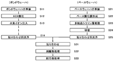
- the process flow of the manufacturing method of the bonded SOI wafer described in Patent Document 1 and Patent Document 2 is shown in FIG. As shown in FIG. 6, in these bonded SOI wafer manufacturing methods, after depositing a polycrystalline silicon layer on a base wafer (S23), the surface of the polycrystalline silicon layer is polished (S24), The pasting (S31) is described.
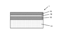
- FIG. 7 shows an example of a cross section of the bonded SOI wafer manufactured as described above. In the bonded SOI wafer 1 shown in FIG. 7, a polycrystalline silicon layer 12, a buried oxide film layer (BOX layer) 16, and an SOI layer 15 are formed in this order on a base wafer 11.
- BOX layer buried oxide film layer
- pit defects are one of the causes of void defects in bonded SOI wafers in the manufacturing process of bonded substrates. Therefore, it is required to reduce the incidence of pit defects and to detect pits with high sensitivity to prevent outflow to the bonding process.
- a defect inspection apparatus As a current method for detecting surface defects, there is a method of detecting by a defect inspection apparatus based on the detection principle of light scattering method or differential interference method.
- the size and number of standards are provided for the surface defects detected by these defect inspection apparatuses, thereby preventing outflow to the bonding process.
- the void generation rate in the bonding process can be reduced, but at the same time, the production yield of the bonding substrate is deteriorated.
- the void generation rate after bonding can be reduced. From such a background, in the manufacturing process of the bonding substrate, there has been a demand for an evaluation method for surface defects that detects only defects that cause voids with high sensitivity.
- the present invention has been made in view of the above problems, and is capable of manufacturing a bonding substrate by detecting a surface defect of a bonding substrate that causes a void defect in a bonded SOI wafer with high sensitivity. It is an object of the present invention to provide a method for evaluating surface defects of a bonding substrate that can reasonably avoid a decrease in yield and reduce the incidence of void defects after bonding.
- the present invention is a method for evaluating a surface defect of a bonding substrate, Preparing a mirror-finished silicon single crystal substrate; Inspecting the surface defects of the mirror-finished silicon single crystal substrate; Depositing a polycrystalline silicon layer on the surface of the silicon single crystal substrate for defect inspection; Performing a mirror chamfer on the silicon single crystal substrate on which the polycrystalline silicon layer is deposited; Polishing the surface of the polycrystalline silicon layer; Inspecting the surface defects of the polished polycrystalline silicon layer; The coordinates of the defects detected in the step of inspecting the surface defects of the silicon single crystal substrate and the step of inspecting the surface defects of the polycrystalline silicon layer are compared.
- a step of performing pass / fail judgment as a bonding substrate of a silicon single crystal substrate having is provided a method for evaluating a surface defect of a bonding substrate characterized by comprising:
- the bonding substrate is a base wafer of a bonded SOI wafer.
- the surface defect evaluation method of the bonding substrate of the present invention is suitable for the manufacturing process of the bonded SOI wafer for the leading-edge high-frequency device. Can be applied to.
- both the surface of the mirror-finished silicon single crystal substrate before deposition of the polycrystalline silicon layer and the surface of the polycrystalline silicon layer after polishing after deposition of the polycrystalline silicon layer are free from surface defects.
- the present inventors have found that the polycrystalline silicon layer has a PW (Polished Wafer) surface before deposition and a polycrystal silicon layer after polishing after deposition.
- PW Poly Wafer
- the present invention has been completed.
- the relationship between the defects on the PW surface and the polished polycrystalline silicon layer surface was investigated.
- the polycrystalline silicon layer is deposited with a thickness of 2 to 3 ⁇ m and then polished to 0.4 to 1 ⁇ m to reduce the surface roughness.
- the detection threshold is used. Measurement was performed at 250 nm. When the defect coordinates of both were compared and verified, it was found that a defect was present at the same position.
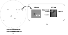
- FIG. 2 is a superposition map (FIG. 2A) of the surface LPD before and after deposition of the polycrystalline silicon layer and a surface SEM / cross-sectional TEM image (FIG. 2B) of the defect detected at the same position.
- FIG. 2A the position of surface defects before the deposition of the polycrystalline silicon layer and the position of surface defects after the deposition of the polycrystalline silicon layer often coincide.
- FIG. 2B shows an example of a result obtained by analyzing a surface defect in which these positions coincide with each other using a surface SEM (Scanning Electron Microscope) and a cross-sectional TEM (Transmission Electron Microscope). From the analysis by the cross-sectional TEM, it was found that the defects on the PW surface were pits, and the defects on the surface of the polycrystalline silicon layer were also pits.
- a bonded SOI wafer was manufactured using this bonding substrate, the entire surface of the wafer was scanned with a bright field optical microscope, an image was captured, and a void defect was extracted by comparing the contrast of the image. Thereafter, the void defect coordinates were further superimposed on the above-described overlay map. The results are shown in FIG. As shown in the overlay map of FIG. 4, it was found that defects detected at the same position before and after the deposition of the polycrystalline silicon layer become 100% voids after bonding.
- this discovery can be said to be the discovery of an evaluation method that can detect only defects that cause voids in bonded SOI wafers with high sensitivity.
- this evaluation method By incorporating this evaluation method into the manufacturing process of the bonding substrate, only wafers having defects that cause voids can be selectively made defective, resulting in a manufacturing yield loss of the bonding substrate. (Excessive production yield reduction) can be reasonably avoided.
- the standard for determining the quality of a bonded substrate was set only by the number of surface defects of the polycrystalline silicon layer.
- a wafer having only defects that do not cause voids may be made defective, so that the production yield of the bonding substrate is unnecessarily lowered. It was.
- a mirror-finished silicon single crystal substrate (PW: Polished Wafer) is prepared (step A).
- PW Polished Wafer
- a general method for producing a silicon single crystal substrate can be used. Specifically, single crystal pulling, cylindrical grinding, notching, slicing, chamfering, lapping, etching, A silicon single crystal substrate that has undergone double-side polishing, mirror chamfering, finish polishing, or the like can be used.
- the surface defect of the mirror-finished silicon single crystal substrate is inspected (step B).
- the surface defect inspection is preferably performed on the surface of the silicon single crystal substrate that has been subjected to final cleaning after finish polishing.
- the detection threshold for detecting a pit in question is preferably 250 nm or more.
- coordinate data of all detected defects are acquired and recorded. The coordinate data can be acquired as a KLARF file if the defect detector is Surfscan SPX manufactured by KLA-Tencor.
- the standard in this step is not set at all or is set to be extremely loose.
- a polycrystalline silicon layer is deposited on the surface of the silicon single crystal substrate subjected to defect inspection (step C).
- the deposition of the polycrystalline silicon layer can be performed according to the technique described in Patent Document 2, for example.
- the film thickness of the polycrystalline silicon layer is, for example, 1 to 5 ⁇ m, preferably 2 to 3 ⁇ m, considering the subsequent polishing allowance.
- hydrophilic surface treatment such as cleaning with SC1 (mixed aqueous solution of NH 4 OH and H 2 O 2 ) and SC2 (mixed aqueous solution of HCl and H 2 O 2 ), ozone water cleaning, and the like. It is preferable to perform washing for the purpose. By making the surface hydrophilic, adhesion of slurry burn can be prevented in the next mirror chamfering step.
- mirror chamfering is performed on the silicon single crystal substrate on which the polycrystalline silicon layer is deposited (step D).
- This mirror chamfering is a mirror chamfering process similar to that used in the manufacturing process of a mirror-finished silicon single crystal substrate in order to remove the polycrystalline silicon film grown on the wafer edge.
- a workpiece holding material called a template attached to the polishing head is used.
- the template is a composite base material of a glass epoxy resin ring and a backing pad, and the inner peripheral wall of the glass epoxy resin ring and the silicon single crystal substrate edge are always in contact during polishing.
- the mirror chamfering is performed here in order to reduce dust generation from the edge portion and sliding resistance with the inner peripheral wall of the ring.
- the surface of the polycrystalline silicon layer is polished (E process).
- surface polishing similar to that performed in the manufacturing process of the mirror-finished silicon single crystal substrate is performed on the surface of the polycrystalline silicon layer.
- the polishing allowance is preferably 0.4 ⁇ m or more for improving the surface roughness. Further, the productivity can be increased by setting the polishing allowance to 1 ⁇ m or less.
- the surface defect of the polished polycrystalline silicon layer is inspected (F process).
- measurement is performed with the same inspection tool and threshold conditions as those in the step of inspecting the surface defect of the silicon single crystal substrate (step B) on the surface of the polycrystalline silicon layer that has been subjected to final cleaning after polishing.
- the coordinate data of all detected defects is acquired and recorded in the same manner as in the B process.
- the coordinates of the defects detected in the step of inspecting the surface defect of the silicon single crystal substrate (step B) and the step of inspecting the surface defect of the polycrystalline silicon layer (step F) are compared, and the defect at the same position Whether or not a silicon single crystal substrate having a polycrystalline silicon layer is a bonding substrate is determined based on the presence or absence (G process).
- the distance between the two defects is within 500 ⁇ m, it can be regarded as the same defect. Only the bonding substrate having the defect determined to be at the same position can be determined as defective, and the others can be determined as non-defective products. Then, the bonding substrate determined to be non-defective can be put into the bonding process.
- the silicon single crystal substrate can be referred to as a bonding substrate when the deposited polycrystalline silicon layer has been polished.
- FIG. 5 shows a process flow diagram of a conventional method for evaluating surface defects of a bonding substrate.
- the steps H, J, K, and L are the same as the steps A, C, D, and E in the method for evaluating surface defects of the bonding substrate according to the present invention, and thus the description is omitted to avoid duplication. To do.
- the conventional method for evaluating surface defects of a bonding substrate has a step (step I) of inspecting a surface defect of a mirror-finished silicon single crystal substrate, but it is not necessary to record coordinates of the detected defect. Furthermore, the conventional method for evaluating the surface defect of the bonding substrate includes a step (M step) of inspecting the surface defect of the polished polycrystalline silicon layer.
- a standard for determining whether or not a bonding substrate is good is provided only for the number of defects detected in this step. Therefore, if the defect number standard is set loosely in order to increase the production yield of the bonding substrate, the void defect occurrence rate of the bonded SOI wafer increases, and conversely, the void defect occurrence rate of the bonded SOI wafer decreases. For this reason, if the above-mentioned standard for the number of defects is set strictly, the manufacturing yield of the bonding substrate is excessively lowered.
- the surface of the mirror-processed silicon single crystal substrate before the deposition of the polycrystalline silicon layer and the polycrystalline after polishing after the deposition of the polycrystalline silicon layer By conducting surface defect inspection on both surfaces of the silicon layer and making only the bonding substrate having the surface defect at the same position as a defective product, it is possible to rationally avoid a decrease in the manufacturing yield of the bonding substrate and It is possible to simultaneously reduce the void defect generation rate of the bonded SOI wafer.
- the bonding substrate used in the method for evaluating surface defects of the bonding substrate of the present invention is a base wafer of a bonded SOI wafer.
- the surface defect evaluation method of the bonding substrate of the present invention is preferably applied to the manufacturing process of the bonded SOI wafer for the high-frequency device at the tip. Can do. As a result, a high-quality bonded SOI wafer can be manufactured at low cost.
- Example 1 100 mirror-finished silicon single crystal substrates (diameter 300 mm, crystal orientation ⁇ 100>) were prepared.
- SurfScan SP2 from KLA-Tencor was used, and the defect size detection threshold was set to 250 nm. After the defect inspection, the coordinates of the detected defects were recorded.
- a polycrystalline silicon layer having a thickness of 3 ⁇ m was deposited on the surface of the silicon single crystal substrate subjected to the defect inspection, and SC1 and SC2 cleaning was performed. Thereafter, mirror chamfering was performed on a silicon single crystal substrate on which polycrystalline silicon was deposited.
- the polishing allowance was 1 ⁇ m
- the polycrystalline silicon layer was polished, and SC1 and SC2 cleaning was performed. Thereafter, the surface of the polished polycrystalline silicon layer was inspected using SurfScan SP2 under the same conditions as described above, and the coordinates of the detected defects were recorded.
- the defect coordinates on the surface of the mirror-finished silicon single crystal substrate are compared with the defect coordinates on the surface of the polished polycrystalline silicon layer. If the distance between the two defects is within 500 ⁇ m, the defect at the same position Therefore, the evaluation target bonding substrate having a defect at the same position was regarded as a defective product. The production yield of the bonding substrate at this time was 97%. Further, a non-defective bonding substrate was used as a base wafer in a bonding SOI process to manufacture a bonded SOI wafer. The voids of the bonded SOI wafer were measured by scanning the entire wafer surface with a bright-field optical microscope, capturing an image, and extracting defects by comparing the contrast of the image.
- the detection threshold at this time was 10 ⁇ m.
- the void (defect) occurrence rate (the ratio of the wafer in which the void defect occurred in the manufactured bonded SOI wafer) was 2.0%. The above results for the examples are shown in Table 1.
- Comparative Example 1 100 mirror-finished silicon single crystal substrates were prepared. For surface defect inspection of these mirror-finished silicon single crystal substrates, SurfScan SP2 from KLA-Tencor was used, and the defect size detection threshold was set to 250 nm. Here, all the substrates were treated as non-defective products without setting standards. Subsequently, a polycrystalline silicon layer having a thickness of 3 ⁇ m was deposited on the surface of the silicon single crystal substrate subjected to the defect inspection, and SC1 and SC2 cleaning was performed. Thereafter, mirror chamfering was performed on a silicon single crystal substrate on which polycrystalline silicon was deposited. Next, the polishing allowance was 1 ⁇ m, the polycrystalline silicon layer was polished, and then SC1 and SC2 cleaning was performed. Thereafter, the surface of the polished polycrystalline silicon layer was inspected under the same conditions as described above using SurfScan SP2, and the number of defects was determined. In Comparative Example 1, the defect number standard was three. The manufacturing yield of the bonding substrate at this time was 96%.
- a non-defective bonding substrate was used as a base wafer in a bonding SOI process to manufacture a bonded SOI wafer.
- the voids of the bonded SOI wafer were measured by scanning the entire surface of the wafer with a bright-field optical microscope, capturing an image, and extracting defects by comparing the contrast of the image.
- the detection threshold at this time was 10 ⁇ m.
- the void generation rate at this time was 7.2%.
- Comparative Example 2 In Comparative Example 2, the quality of the bonded substrate was determined in the same manner as in Comparative Example 1 except that the number of defects on the surface of the polished polycrystalline silicon layer was set to 2. The manufacturing yield of the bonding substrate at that time was 95%. Furthermore, when the void generation rate was determined in the same manner as in Comparative Example 1, it was 6.3%. The results of Comparative Example 2 are shown in Table 1.
- Comparative Example 3 In Comparative Example 3, whether or not the bonding substrate was good was determined in the same manner as in Comparative Example 1 except that the number of defects on the surface of the polished polycrystalline silicon layer was set to 1. The manufacturing yield of the bonding substrate at that time was 93%. Further, when the void generation rate was determined in the same manner as in Comparative Example 1, it was 3.2%. The results of Comparative Example 3 are shown in Table 1.
- the production yield of the bonding substrate was high, and the void generation rate was low.
- the void generation rate was improved instead of lowering the manufacturing yield by lowering the defect number standard of the bonding substrate.
- the present invention is not limited to the above embodiment.
- the above-described embodiment is an exemplification, and the present invention has substantially the same configuration as the technical idea described in the claims of the present invention, and any device that exhibits the same function and effect is the present invention. It is included in the technical scope of the invention.
Landscapes
- General Health & Medical Sciences (AREA)
- Health & Medical Sciences (AREA)
- Life Sciences & Earth Sciences (AREA)
- Chemical & Material Sciences (AREA)
- Analytical Chemistry (AREA)
- Biochemistry (AREA)
- Physics & Mathematics (AREA)
- General Physics & Mathematics (AREA)
- Immunology (AREA)
- Pathology (AREA)
- Testing Or Measuring Of Semiconductors Or The Like (AREA)
- Investigating Materials By The Use Of Optical Means Adapted For Particular Applications (AREA)
- Mechanical Treatment Of Semiconductor (AREA)
Abstract
本発明は、鏡面加工されたシリコン単結晶基板を準備する工程と、鏡面加工されたシリコン単結晶基板の表面欠陥を検査する工程と、シリコン単結晶基板の欠陥検査を行った表面に多結晶シリコン層を堆積する工程と、多結晶シリコン層を堆積したシリコン単結晶基板に鏡面面取りを行う工程と、多結晶シリコン層の表面を研磨する工程と、研磨された多結晶シリコン層の表面欠陥を検査する工程と、シリコン単結晶基板の表面欠陥の検査工程と多結晶シリコン層の表面欠陥の検査工程で検出された欠陥の座標を比較し、同一位置にある欠陥の有無で、多結晶シリコン層を有するシリコン単結晶基板の貼り合わせ用基板としての良否判定を行う工程とを有する貼り合わせ用基板の表面欠陥の評価方法である。これにより、貼り合わせ用基板の製造歩留の低下を合理的に回避し、貼り合せ後のボイド欠陥発生率を低減することができる貼り合わせ用基板の表面欠陥の評価方法が提供される。
Description
本発明は、貼り合わせ用基板の表面欠陥の評価方法に関する。
先端の高周波デバイス向け貼り合わせSOIウェーハプロセスでは、貼り合わせ用基板として、表層に多結晶シリコン層を形成したシリコン基板をベースウェーハとして用いることがある。このベースウェーハと別途ボンドウェーハを用意して両者を貼り合わせた後、ボンドウェーハを薄膜化することで貼り合わせSOIウェーハが作製される。
特許文献1及び特許文献2には、いずれも多結晶シリコン層をキャリアトラップ層(トラップリッチ(Trap-Rich)層とも呼ばれる。)とする、高周波デバイス向け貼り合わせSOIウェーハの製造方法が記載されている。特許文献1及び特許文献2に記載された貼り合わせSOIウェーハの製造方法の工程フローを図6に示した。図6に示すように、これらの貼り合わせSOIウェーハの製造方法では、ベースウェーハに多結晶シリコン層を堆積(S23)した後、その多結晶シリコン層の表面を研磨(S24)し、ボンドウェーハと貼り合わせる(S31)ことが記載されている。また、このようにして製造された貼り合わせSOIウェーハの断面の一例を図7に示す。図7に示した貼り合わせSOIウェーハ1では、ベースウェーハ11上に、多結晶シリコン層12、埋め込み酸化膜層(BOX層)16、及びSOI層15がこの順に形成されている。
貼り合わせSOIウェーハの主な不良項目として、ボイド欠陥と呼ばれる局所的な未接着領域が挙げられ、その改善が求められている。貼り合わせ用基板の製造工程において、ピット欠陥が貼り合わせSOIウェーハのボイド欠陥の原因の一つであることが知られている。その為、ピット欠陥発生率を低減することと、ピットを高感度で検出して貼り合わせ工程への流出を防止することが要求されている。
現在の表面欠陥の検出方法としては、光散乱法又は微分干渉法を検出原理とした欠陥検査装置によって検出する方法がある。貼り合わせウェーハの製造プロセスにおいて、これらの欠陥検査装置で検出された表面欠陥に対して、サイズと個数の規格を設けることで、貼り合せ工程への流出を防止している。個数の規格の上限を下げていくことで、貼り合わせ工程でのボイド発生率を低減できるが、同時に貼り合わせ用基板の製造歩留を悪化させてしまうという問題が生じる。この時、もしボイドの原因となる欠陥のみを効率的に検出できれば、貼り合わせ用基板の製造歩留の無用なロスを回避でき、かつ、貼り合わせ後のボイド発生率も低減可能となる。このような背景から、貼り合わせ用基板の製造工程において、ボイドの原因となる欠陥だけを高感度で検出する表面欠陥の評価方法が求められていた。
本発明は、上記問題点に鑑みてなされたものであって、貼り合わせSOIウェーハにおけるボイド欠陥の原因となる貼り合せ用基板の表面欠陥を高感度で検出することで、貼り合わせ用基板の製造歩留の低下を合理的に回避し、貼り合せ後のボイド欠陥発生率を低減することができる貼り合わせ用基板の表面欠陥の評価方法を提供することを目的とする。
上記目的を達成するために、本発明は、貼り合わせ用基板の表面欠陥の評価方法であって、
鏡面加工されたシリコン単結晶基板を準備する工程と、
前記鏡面加工されたシリコン単結晶基板の表面欠陥を検査する工程と、
前記シリコン単結晶基板の欠陥検査を行った表面に多結晶シリコン層を堆積する工程と、
前記多結晶シリコン層を堆積したシリコン単結晶基板に鏡面面取りを行う工程と、
前記多結晶シリコン層の表面を研磨する工程と、
前記研磨された多結晶シリコン層の表面欠陥を検査する工程と、
前記シリコン単結晶基板の表面欠陥を検査する工程と前記多結晶シリコン層の表面欠陥を検査する工程で検出された欠陥の座標を比較し、同一位置にある欠陥の有無で、前記多結晶シリコン層を有するシリコン単結晶基板の貼り合わせ用基板としての良否判定を行う工程と、
を有することを特徴とする貼り合わせ用基板の表面欠陥の評価方法を提供する。
鏡面加工されたシリコン単結晶基板を準備する工程と、
前記鏡面加工されたシリコン単結晶基板の表面欠陥を検査する工程と、
前記シリコン単結晶基板の欠陥検査を行った表面に多結晶シリコン層を堆積する工程と、
前記多結晶シリコン層を堆積したシリコン単結晶基板に鏡面面取りを行う工程と、
前記多結晶シリコン層の表面を研磨する工程と、
前記研磨された多結晶シリコン層の表面欠陥を検査する工程と、
前記シリコン単結晶基板の表面欠陥を検査する工程と前記多結晶シリコン層の表面欠陥を検査する工程で検出された欠陥の座標を比較し、同一位置にある欠陥の有無で、前記多結晶シリコン層を有するシリコン単結晶基板の貼り合わせ用基板としての良否判定を行う工程と、
を有することを特徴とする貼り合わせ用基板の表面欠陥の評価方法を提供する。
このように、鏡面加工されたシリコン単結晶基板の表面と、多結晶シリコン層の堆積後に研磨を行った後の多結晶シリコン層の表面の両者で表面欠陥の検査を行い、同一位置に表面欠陥を有する貼り合わせ用基板のみを不良品とすることで、貼り合わせ用基板の製造歩留の低下の合理的な回避及び貼り合わせSOIウェーハのボイド欠陥発生率低減を両立させることができる。
このとき、前記貼り合わせ用基板は、貼り合わせSOIウェーハのベースウェーハであることが好ましい。
このように、貼り合わせ用基板を貼り合わせSOIウェーハのベースウェーハとすることで、本発明の貼り合わせ用基板の表面欠陥の評価方法を、先端の高周波デバイス向け貼り合わせSOIウェーハの製造プロセスに好適に適用することができる。
本発明によれば、多結晶シリコン層堆積前の鏡面加工されたシリコン単結晶基板の表面と、多結晶シリコン層の堆積後に研磨を行った後の多結晶シリコン層の表面の両者で表面欠陥の検査を行い、同一位置に表面欠陥を有する貼り合わせ用基板のみを不良品とすることで、貼り合わせ用基板の製造歩留ロスの回避及び貼り合わせSOIウェーハのボイド欠陥発生率低減を両立させることができる。
上記のように、貼り合わせ用基板の表面欠陥の評価方法において、貼り合わせ用基板の製造歩留のロスを回避し、かつ、貼り合わせSOIウェーハのボイド欠陥発生率を低減することができる貼り合わせ用基板の表面欠陥の評価方法が求められている。
本発明者らは、上記目的を達成するために鋭意検討を行った結果、多結晶シリコン層を堆積前のPW(Polished Wafer)表面と、多結晶シリコン層の堆積後に研磨を行った後の多結晶シリコン層表面の両者で表面欠陥の検査を行い、同一位置に表面欠陥を有するウェーハのみを不良品とすることで、上記課題を解決できることを見出し、本発明を完成させた。
以下、本発明について、図を参照しながら詳細に説明するが、本発明はこれらに限定されるものではない。
まず、PW表面の欠陥と研磨された多結晶シリコン層表面の欠陥の関係について調査した。通常、上述した貼り合わせ用基板においては、多結晶シリコン層は2~3μmの厚さで堆積された後、表面粗さを低減する為に0.4~1μm研磨される。多結晶シリコン層堆積前のPW表面と、多結晶シリコン層堆積後かつ研磨後の多結晶シリコン層表面に対して、KLA-TENCOR社製のSurfScan SP2等の表面欠陥検査機を用いて、検出閾値250nmとして測定を行った。両者の欠陥座標を比較照合したところ、同一位置に欠陥が存在することが分かった。
この同一位置に存在する欠陥について詳細に解析を行った。図2は、多結晶シリコン層堆積前後の表面LPDの重ね合わせマップ(図2(a))及び同一位置に検出された欠陥の表面SEM/断面TEM像(図2(b))である。図2(a)に示したように、多結晶シリコン層堆積前の表面欠陥の位置と多結晶シリコン層堆積後の表面欠陥の位置は、一致しているものが多い。これらの位置が一致した表面欠陥を表面SEM(Scanning Electron Microscope)と断面TEM(Transmission Electron Microscope)で解析した結果の一例が図2(b)である。断面TEMによる解析から、PW表面の欠陥はピットであり、多結晶シリコン層表面の欠陥もピットであることが分かった。
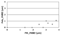
さらに評価及び解析を行ったところ、PW表面のピット深さと研磨後の多結晶シリコン層表面のピット深さは図3に示す関係にあることが分かった。
図3に示した結果から、PW表面に深さ3μm以上のピットがあると、多結晶シリコン層でそのピットを埋めることができず、研磨を行ったとしても多結晶シリコン層表面にもピットが残留してしまうことを見出した。これとは逆に、PW表面のピット深さが3μm未満であれば多結晶シリコン層で埋められるか、又は、完全に埋められなくても研磨で平坦化されるかのどちらかであることを示している。
さらに、この貼り合わせ用基板を用いて貼り合わせSOIウェーハを作製し、明視野の光学顕微鏡でウェーハ表面全面をスキャンして画像を取り込み、画像のコントラストの比較によってボイド欠陥を抽出した。その後、前述の重ね合わせマップにボイド欠陥の座標をさらに重ね合わせた。その結果を図4に示した。図4の重ね合わせマップに示すように、多結晶シリコン層堆積前後で同一位置に検出された欠陥は、貼り合わせ後に100%ボイドとなることを見出した。
この発見は視点を変えれば、貼り合わせSOIウェーハのボイドの原因となる欠陥のみを高感度に検出できる評価方法の発見であるといえる。この評価方法を貼り合せ用基板の製造プロセスに組み込むことにより、ボイドの原因となる欠陥を有するウェーハのみを選択的に不良品とすることができ、結果的に貼り合わせ用基板の製造歩留ロス(過剰な製造歩留の低下)を合理的に回避することができる。
従来の貼り合わせSOIウェーハの製造プロセスでは、多結晶シリコン層の表面欠陥個数でのみ、貼り合わせ用基板の良否判定の規格を設定していた。しかし、これでは、図4に示すように、ボイドの原因とはならない欠陥だけを有するウェーハをも不良としてしまうことがあるため、貼り合わせ用基板の製造歩留を必要以上に低下させてしまっていた。
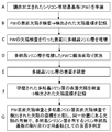
次に、図1に示した、本発明の貼り合わせ用基板の表面欠陥の評価方法の工程フロー図を参照して、本発明についてさらに詳細に説明する。
まず、鏡面加工されたシリコン単結晶基板(PW:Polished Wafer)を準備する(A工程)。準備するシリコン単結晶基板の製造には、一般的なシリコン単結晶基板の製造方法を用いることができ、具体的には、単結晶引き上げ、円筒研削、ノッチ加工、スライス、面取り、ラッピング、エッチング、両面研磨、鏡面面取り、仕上げ研磨等を経たシリコン単結晶基板を用いることができる。
次に、鏡面加工されたシリコン単結晶基板の表面欠陥を検査する(B工程)。表面欠陥の検査は、仕上げ研磨後、最終洗浄を通したシリコン単結晶基板表面に対して行うことが好ましい。表面欠陥検査ツールとして、KLA-Tencor社製のSurfscan SPX(X=1~3)を用いることができ、暗視野での散乱光をLPDとして検出する。問題となるピットを検出するための検出閾値は250nm以上とすることが好ましい。このとき、検出された全欠陥の座標データを取得、記録する。座標データは、欠陥検出機がKLA-Tencor社製のSurfscan SPXであればKLARFファイルとして取得することができる。この工程で規格を設定することも可能であるが、その後の多結晶シリコン層の堆積によりピットが完全に埋められる、又は、完全に埋められなくとも、後工程の研磨で平坦化されるほどの浅いピットとして残るかで、救済される欠陥もある。そのため、鏡面加工されたシリコン単結晶基板の製造歩留の観点からは、本工程での規格は全く設定しないか、又は、極めて緩い設定とすることが好ましい。
次に、シリコン単結晶基板の欠陥検査を行った表面に多結晶シリコン層を堆積する(C工程)。多結晶シリコン層の堆積は、例えば、特許文献2に記載の技術に従って行うことができる。多結晶シリコン層の膜厚は、後の研磨取代を考慮して、例えば1~5μm、好ましくは2~3μmとする。また、多結晶シリコン層形成後は、SC1(NH4OHとH2O2の混合水溶液)とSC2(HClとH2O2の混合水溶液)による洗浄や、オゾン水洗浄等の親水面化処理のための洗浄を行うことが好ましい。親水面化されることで、次の鏡面面取り工程で、スラリーバーンの付着を防止することができる。
その後、多結晶シリコン層を堆積したシリコン単結晶基板に鏡面面取りを行う(D工程)。この鏡面面取りは、鏡面加工されたシリコン単結晶基板の製造工程で用いられるのと同様の鏡面面取り加工を、ウェーハエッジ部に成長した多結晶シリコン膜を除去するために行うものである。その後の研磨工程では、研磨ヘッドに取り付けられたテンプレートと呼ばれるワーク保持材を用いる。テンプレートはガラスエポキシ樹脂製リングとバッキングパッドの複合基材であり、研磨中はこのガラスエポキシ樹脂製リングの内周壁とシリコン単結晶基板エッジ部が常時接触することとなる。つまり、ここで鏡面面取りを行うのは、エッジ部からの発塵やリング内周壁との摺動抵抗の低減のためである。
次に、多結晶シリコン層の表面を研磨する(E工程)。この工程では、鏡面加工されたシリコン単結晶基板の製造工程で行われるのと同様の表面研磨を多結晶シリコン層表面に対して行う。研磨取代は0.4μm以上とすることが面粗さ改善のために好ましい。また、研磨取代を1μm以下とすることで生産性を高めることができる。
次に、研磨された多結晶シリコン層の表面欠陥を検査する(F工程)。この工程では、シリコン単結晶基板の表面欠陥を検査する工程(B工程)と同様の検査ツール、閾値条件での測定を、研磨後に最終洗浄を通した多結晶シリコン層表面に対して行う。検出された全欠陥の座標データをB工程と同様に取得、記録する。
さらに、シリコン単結晶基板の表面欠陥を検査する工程(B工程)と多結晶シリコン層の表面欠陥を検査する工程(F工程)で検出された欠陥の座標を比較し、同一位置にある欠陥の有無で、多結晶シリコン層を有するシリコン単結晶基板の貼り合わせ用基板としての良否判定を行う(G工程)。ここで、欠陥測定における座標精度を考慮して、両欠陥の距離が500μm以内であれば同一の欠陥とみなすことができる。同一位置と判断された欠陥を有する貼り合わせ用基板のみを不良とし、それ以外は良品と判断することができる。そして、良品と判断された貼り合わせ用基板は貼り合わせ工程に投入することができる。尚、シリコン単結晶基板は堆積された多結晶シリコン層の研磨まで終わった段階で、貼り合わせ用基板と呼ぶことができる。
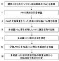
比較のために、従来の貼り合わせ用基板の表面欠陥の評価方法の工程フロー図を図5に示した。図5において、H、J、K及びL工程については、本発明の貼り合わせ用基板の表面欠陥の評価方法のA、C、D及びE工程と共通であるため、重複を避けるため説明は省略する。
従来の貼り合わせ用基板の表面欠陥の評価方法では、鏡面加工されたシリコン単結晶基板の表面欠陥を検査する工程(I工程)を有するが、検出された欠陥の座標は記録する必要がない。さらに従来の貼り合わせ用基板の表面欠陥の評価方法は、研磨された多結晶シリコン層の表面欠陥を検査する工程(M工程)を有する。従来は、この工程で検出された欠陥個数に対してのみ、貼り合わせ用基板の良否判定の規格を設けていた。そのため、貼り合わせ用基板の製造歩留を高めるために欠陥個数の規格を緩く設定すると、貼り合わせSOIウェーハのボイド欠陥発生率が高くなり、反対に、貼り合わせSOIウェーハのボイド欠陥発生率を下げるために前述の欠陥個数の規格を厳しく設定すると、貼り合わせ用基板の製造歩留を過剰に低下させてしまっていた。
本発明の貼り合わせ用基板の表面欠陥の評価方法では、多結晶シリコン層の堆積前の鏡面加工されたシリコン単結晶基板の表面と、多結晶シリコン層の堆積後に研磨を行った後の多結晶シリコン層の表面の両者で表面欠陥の検査を行い、同一位置に表面欠陥を有する貼り合わせ用基板のみを不良品とすることで、貼り合わせ用基板の製造歩留の低下の合理的な回避及び貼り合わせSOIウェーハのボイド欠陥発生率低減を両立させることができる。
また、本発明の貼り合わせ用基板の表面欠陥の評価方法で用いる貼り合わせ用基板は、貼り合わせSOIウェーハのベースウェーハであることが好ましい。貼り合わせ用基板を貼り合わせSOIウェーハのベースウェーハとすることで、本発明の貼り合わせ用基板の表面欠陥の評価方法を、先端の高周波デバイス向け貼り合わせSOIウェーハの製造プロセスに好適に適用することができる。その結果、高品質の貼り合わせSOIウェーハを安価に製造することができる。
以下、実施例及び比較例を示して本発明をより具体的に説明するが、本発明はこれらに限定されるものではない。
(実施例)
まず、鏡面加工されたシリコン単結晶基板(直径300mm、結晶方位<100>)を100枚準備した。これらの鏡面加工されたシリコン単結晶基板の表面欠陥検査にはKLA-Tencor社のSurfScan SP2を用い、欠陥サイズの検出閾値を250nmとした。欠陥検査後、検出された欠陥の座標を記録した。続いて、欠陥検査を行ったシリコン単結晶基板の表面上に膜厚3μmの多結晶シリコン層を堆積し、SC1及びSC2洗浄を行った。その後、多結晶シリコンを堆積したシリコン単結晶基板に鏡面面取りを実施した。次に、研磨取代を1μmとして、多結晶シリコン層を研磨し、SC1及びSC2洗浄を行った。その後、研磨された多結晶シリコン層の表面をSurfScan SP2を用いて前述したのと同じ条件で検査し、検出された欠陥の座標を記録した。
まず、鏡面加工されたシリコン単結晶基板(直径300mm、結晶方位<100>)を100枚準備した。これらの鏡面加工されたシリコン単結晶基板の表面欠陥検査にはKLA-Tencor社のSurfScan SP2を用い、欠陥サイズの検出閾値を250nmとした。欠陥検査後、検出された欠陥の座標を記録した。続いて、欠陥検査を行ったシリコン単結晶基板の表面上に膜厚3μmの多結晶シリコン層を堆積し、SC1及びSC2洗浄を行った。その後、多結晶シリコンを堆積したシリコン単結晶基板に鏡面面取りを実施した。次に、研磨取代を1μmとして、多結晶シリコン層を研磨し、SC1及びSC2洗浄を行った。その後、研磨された多結晶シリコン層の表面をSurfScan SP2を用いて前述したのと同じ条件で検査し、検出された欠陥の座標を記録した。
さらに、鏡面加工されたシリコン単結晶基板の表面の欠陥座標と、研磨された多結晶シリコン層の表面の欠陥座標を比較照合し、両欠陥の間の距離が500μm以内であれば同一位置の欠陥と見なし、同一位置の欠陥を有する評価対象の貼り合わせ用基板を不良品とした。このときの貼り合わせ用基板の製造歩留は97%であった。さらに、良品の貼り合せ用基板をベースウェーハとして貼り合わせSOIプロセスに投入して、貼り合わせSOIウェーハを製造した。貼り合わせSOIウェーハのボイドの測定は、明視野の光学顕微鏡でウェーハ表面全体をスキャンして画像を取り込み、画像のコントラストの比較によって欠陥を抽出することで行った。この際の検出閾値は10μmとした。このときのボイド(欠陥)発生率(製造した貼り合わせSOIウェーハ中のボイド欠陥が発生したウェーハの割合)は2.0%であった。実施例についての以上の結果を表1に示した。

(比較例1)
まず、鏡面加工されたシリコン単結晶基板を100枚準備した。これらの鏡面加工されたシリコン単結晶基板の表面欠陥検査にはKLA-Tencor社のSurfScan SP2を用い、欠陥サイズの検出閾値を250nmとした。ここでは規格を設けずに全ての基板を良品扱いとした。続いて、欠陥検査を行ったシリコン単結晶基板の表面上に膜厚3μmの多結晶シリコン層を堆積し、SC1及びSC2洗浄を行った。その後、多結晶シリコンを堆積したシリコン単結晶基板に鏡面面取りを実施した。次に、研磨取代を1μmとし、多結晶シリコン層を研磨し、次いでSC1及びSC2洗浄を行った。その後、研磨された多結晶シリコン層の表面をSurfScan SP2を用いて前述したのと同じ条件で検査し、欠陥の個数を求めた。比較例1では、欠陥の個数規格を3個とした。このときの貼り合せ用基板の製造歩留は、96%であった。
まず、鏡面加工されたシリコン単結晶基板を100枚準備した。これらの鏡面加工されたシリコン単結晶基板の表面欠陥検査にはKLA-Tencor社のSurfScan SP2を用い、欠陥サイズの検出閾値を250nmとした。ここでは規格を設けずに全ての基板を良品扱いとした。続いて、欠陥検査を行ったシリコン単結晶基板の表面上に膜厚3μmの多結晶シリコン層を堆積し、SC1及びSC2洗浄を行った。その後、多結晶シリコンを堆積したシリコン単結晶基板に鏡面面取りを実施した。次に、研磨取代を1μmとし、多結晶シリコン層を研磨し、次いでSC1及びSC2洗浄を行った。その後、研磨された多結晶シリコン層の表面をSurfScan SP2を用いて前述したのと同じ条件で検査し、欠陥の個数を求めた。比較例1では、欠陥の個数規格を3個とした。このときの貼り合せ用基板の製造歩留は、96%であった。
そして、良品の貼り合せ用基板をベースウェーハとして貼り合わせSOIプロセスに投入して、貼り合わせSOIウェーハを製造した。貼り合わせSOIウェーハのボイドの測定は、明視野の光学顕微鏡でウェーハ表面全面をスキャンして画像を取り込み、画像のコントラストの比較によって欠陥を抽出することで行った。この際の検出閾値は10μmとした。このときのボイド発生率は7.2%であった。比較例1のこれらの結果を表1に示した。
(比較例2)
比較例2では、研磨された多結晶シリコン層の表面の欠陥の個数規格を2個としたこと以外は、比較例1と同様にして、貼り合せ用基板の良否判定を行った。そのときの貼り合せ用基板の製造歩留は、95%であった。さらに、比較例1と同様にしてボイド発生率を求めたところ、6.3%であった。比較例2のこれらの結果を表1に示した。
比較例2では、研磨された多結晶シリコン層の表面の欠陥の個数規格を2個としたこと以外は、比較例1と同様にして、貼り合せ用基板の良否判定を行った。そのときの貼り合せ用基板の製造歩留は、95%であった。さらに、比較例1と同様にしてボイド発生率を求めたところ、6.3%であった。比較例2のこれらの結果を表1に示した。
(比較例3)
比較例3では、研磨された多結晶シリコン層の表面の欠陥の個数規格を1個としたこと以外は、比較例1と同様にして、貼り合せ用基板の良否判定をおこなった。そのときの貼り合せ用基板の製造歩留は、93%であった。さらに、比較例1と同様にしてボイド発生率を求めたところ、3.2%であった。比較例3のこれらの結果を表1に示した。
比較例3では、研磨された多結晶シリコン層の表面の欠陥の個数規格を1個としたこと以外は、比較例1と同様にして、貼り合せ用基板の良否判定をおこなった。そのときの貼り合せ用基板の製造歩留は、93%であった。さらに、比較例1と同様にしてボイド発生率を求めたところ、3.2%であった。比較例3のこれらの結果を表1に示した。
以上のように、実施例では貼り合わせ用基板の製造歩留は高く、また、ボイド発生率は低かった。一方、比較例1-3では貼り合わせ用基板の欠陥個数規格を下げることで製造歩留が低下するかわりに、ボイド発生率は改善していた。しかしながら、比較例では貼り合わせ用基板の高い製造歩留と貼り合わせSOIウェーハの低いボイド発生率を両立させることはできなかった。従って、本発明の有効性が示された。
なお、本発明は、上記実施形態に限定されるものではない。上記実施形態は、例示であり、本発明の特許請求の範囲に記載された技術的思想と実質的に同一な構成を有し、同様な作用効果を奏するものは、いかなるものであっても本発明の技術的範囲に包含される。
Claims (2)
- 貼り合わせ用基板の表面欠陥の評価方法であって、
鏡面加工されたシリコン単結晶基板を準備する工程と、
前記鏡面加工されたシリコン単結晶基板の表面欠陥を検査する工程と、
前記シリコン単結晶基板の欠陥検査を行った表面に多結晶シリコン層を堆積する工程と、
前記多結晶シリコン層を堆積したシリコン単結晶基板に鏡面面取りを行う工程と、
前記多結晶シリコン層の表面を研磨する工程と、
前記研磨された多結晶シリコン層の表面欠陥を検査する工程と、
前記シリコン単結晶基板の表面欠陥を検査する工程と前記多結晶シリコン層の表面欠陥を検査する工程で検出された欠陥の座標を比較し、同一位置にある欠陥の有無で、前記多結晶シリコン層を有するシリコン単結晶基板の貼り合わせ用基板としての良否判定を行う工程と、
を有することを特徴とする貼り合わせ用基板の表面欠陥の評価方法。 - 前記貼り合わせ用基板は、貼り合わせSOIウェーハのベースウェーハであることを特徴とする請求項1に記載の貼り合わせ用基板の表面欠陥の評価方法。
Priority Applications (5)
| Application Number | Priority Date | Filing Date | Title |
|---|---|---|---|
| EP17848446.5A EP3511976B1 (en) | 2016-09-07 | 2017-07-26 | Bonding substrate surface defect evaluation method |
| KR1020197006354A KR102327328B1 (ko) | 2016-09-07 | 2017-07-26 | 접합용 기판의 표면결함의 평가방법 |
| US16/327,482 US10707140B2 (en) | 2016-09-07 | 2017-07-26 | Method for evaluating surface defects of substrate to be bonded |
| CN201780051581.3A CN109643670B (zh) | 2016-09-07 | 2017-07-26 | 贴合用基板的表面缺陷的评价方法 |
| SG11201901686QA SG11201901686QA (en) | 2016-09-07 | 2017-07-26 | Method for evaluating surface defects of substrate to be bonded |
Applications Claiming Priority (2)
| Application Number | Priority Date | Filing Date | Title |
|---|---|---|---|
| JP2016175044A JP6614076B2 (ja) | 2016-09-07 | 2016-09-07 | 貼り合わせ用基板の表面欠陥の評価方法 |
| JP2016-175044 | 2016-09-07 |
Publications (1)
| Publication Number | Publication Date |
|---|---|
| WO2018047501A1 true WO2018047501A1 (ja) | 2018-03-15 |
Family
ID=61561765
Family Applications (1)
| Application Number | Title | Priority Date | Filing Date |
|---|---|---|---|
| PCT/JP2017/027102 Ceased WO2018047501A1 (ja) | 2016-09-07 | 2017-07-26 | 貼り合わせ用基板の表面欠陥の評価方法 |
Country Status (8)
| Country | Link |
|---|---|
| US (1) | US10707140B2 (ja) |
| EP (1) | EP3511976B1 (ja) |
| JP (1) | JP6614076B2 (ja) |
| KR (1) | KR102327328B1 (ja) |
| CN (1) | CN109643670B (ja) |
| SG (1) | SG11201901686QA (ja) |
| TW (1) | TWI722225B (ja) |
| WO (1) | WO2018047501A1 (ja) |
Cited By (1)
| Publication number | Priority date | Publication date | Assignee | Title |
|---|---|---|---|---|
| CN114034535A (zh) * | 2021-11-09 | 2022-02-11 | 四川华能康定水电有限责任公司 | 现场用涂层质量评估辅助方法和系统 |
Families Citing this family (5)
| Publication number | Priority date | Publication date | Assignee | Title |
|---|---|---|---|---|
| JP7172951B2 (ja) * | 2019-10-31 | 2022-11-16 | 信越半導体株式会社 | 半導体ウェーハの評価方法、半導体ウェーハの選別方法及びデバイスの製造方法 |
| US20230197533A1 (en) * | 2020-06-01 | 2023-06-22 | Shin-Etsu Handotai Co., Ltd. | Method for evaluating peripheral strain of wafer |
| US12176202B2 (en) * | 2020-10-08 | 2024-12-24 | Okmetic Oy | Manufacture method of a high-resistivity silicon handle wafer for a hybrid substrate structure |
| CN112951735B (zh) * | 2021-01-28 | 2022-11-08 | 微龛(广州)半导体有限公司 | 晶圆键合质量检测方法及系统 |
| CN114994058A (zh) * | 2022-06-09 | 2022-09-02 | 杭州利珀科技有限公司 | 硅片堆叠检测系统及方法 |
Citations (2)
| Publication number | Priority date | Publication date | Assignee | Title |
|---|---|---|---|---|
| JP2007192651A (ja) * | 2006-01-19 | 2007-08-02 | Tokyo Seimitsu Co Ltd | 半導体製造装置、半導体外観検査装置、及び外観検査方法 |
| JP2010021242A (ja) * | 2008-07-09 | 2010-01-28 | Sumco Corp | 貼り合わせ用ウェーハの欠陥検出方法 |
Family Cites Families (17)
| Publication number | Priority date | Publication date | Assignee | Title |
|---|---|---|---|---|
| JPH06252230A (ja) * | 1993-02-24 | 1994-09-09 | Hitachi Ltd | 欠陥検査方法および装置 |
| JP3633062B2 (ja) * | 1994-12-22 | 2005-03-30 | 株式会社デンソー | 研磨方法および研磨装置 |
| KR100551570B1 (ko) * | 1999-10-14 | 2006-02-13 | 주식회사 사무코 | 반도체 웨이퍼표면의 검사방법 |
| JP4104396B2 (ja) * | 2002-07-31 | 2008-06-18 | 株式会社ニデック | 外観検査装置 |
| JP4507157B2 (ja) * | 2003-06-17 | 2010-07-21 | 信越半導体株式会社 | ウエーハ製造工程の管理方法 |
| JP2005166846A (ja) | 2003-12-01 | 2005-06-23 | Sumitomo Mitsubishi Silicon Corp | Soi基板のhf欠陥の測定方法 |
| KR20080073584A (ko) * | 2007-02-06 | 2008-08-11 | 주식회사 하이닉스반도체 | 실리콘 웨이퍼의 표면 검사 방법 |
| JP5372365B2 (ja) * | 2007-12-25 | 2013-12-18 | 株式会社日立ハイテクノロジーズ | 検査装置及び検査方法 |
| KR101377240B1 (ko) * | 2009-06-26 | 2014-03-20 | 가부시키가이샤 사무코 | 실리콘 웨이퍼의 세정 방법 및, 그 세정 방법을 이용한 에피택셜 웨이퍼의 제조 방법 |
| TWI498954B (zh) * | 2009-08-21 | 2015-09-01 | 勝高股份有限公司 | 磊晶矽晶圓的製造方法 |
| US9224660B2 (en) * | 2013-08-30 | 2015-12-29 | Kla-Tencor Corp. | Tuning wafer inspection recipes using precise defect locations |
| JP6100200B2 (ja) | 2014-04-24 | 2017-03-22 | 信越半導体株式会社 | 貼り合わせsoiウェーハの製造方法 |
| JP6118757B2 (ja) | 2014-04-24 | 2017-04-19 | 信越半導体株式会社 | 貼り合わせsoiウェーハの製造方法 |
| CN104217973B (zh) * | 2014-09-02 | 2017-03-08 | 上海华力微电子有限公司 | 检测多晶硅栅极氧化层缺失的方法 |
| CN104201131B (zh) * | 2014-09-02 | 2017-03-08 | 上海华力微电子有限公司 | 评估多晶硅栅极氧化层缺失缺陷的方法 |
| JP6045542B2 (ja) * | 2014-09-11 | 2016-12-14 | 信越半導体株式会社 | 半導体ウェーハの加工方法、貼り合わせウェーハの製造方法、及びエピタキシャルウェーハの製造方法 |
| JP6179530B2 (ja) * | 2015-01-23 | 2017-08-16 | 信越半導体株式会社 | 貼り合わせsoiウェーハの製造方法 |
-
2016
- 2016-09-07 JP JP2016175044A patent/JP6614076B2/ja active Active
-
2017
- 2017-07-26 CN CN201780051581.3A patent/CN109643670B/zh active Active
- 2017-07-26 WO PCT/JP2017/027102 patent/WO2018047501A1/ja not_active Ceased
- 2017-07-26 EP EP17848446.5A patent/EP3511976B1/en active Active
- 2017-07-26 US US16/327,482 patent/US10707140B2/en active Active
- 2017-07-26 SG SG11201901686QA patent/SG11201901686QA/en unknown
- 2017-07-26 KR KR1020197006354A patent/KR102327328B1/ko active Active
- 2017-07-31 TW TW106125676A patent/TWI722225B/zh active
Patent Citations (2)
| Publication number | Priority date | Publication date | Assignee | Title |
|---|---|---|---|---|
| JP2007192651A (ja) * | 2006-01-19 | 2007-08-02 | Tokyo Seimitsu Co Ltd | 半導体製造装置、半導体外観検査装置、及び外観検査方法 |
| JP2010021242A (ja) * | 2008-07-09 | 2010-01-28 | Sumco Corp | 貼り合わせ用ウェーハの欠陥検出方法 |
Non-Patent Citations (1)
| Title |
|---|
| See also references of EP3511976A4 * |
Cited By (2)
| Publication number | Priority date | Publication date | Assignee | Title |
|---|---|---|---|---|
| CN114034535A (zh) * | 2021-11-09 | 2022-02-11 | 四川华能康定水电有限责任公司 | 现场用涂层质量评估辅助方法和系统 |
| CN114034535B (zh) * | 2021-11-09 | 2024-04-30 | 四川华能康定水电有限责任公司 | 现场用涂层质量评估辅助方法和系统 |
Also Published As
| Publication number | Publication date |
|---|---|
| KR102327328B1 (ko) | 2021-11-17 |
| EP3511976A1 (en) | 2019-07-17 |
| SG11201901686QA (en) | 2019-03-28 |
| US20190181059A1 (en) | 2019-06-13 |
| TW201820498A (zh) | 2018-06-01 |
| CN109643670B (zh) | 2022-10-11 |
| KR20190043546A (ko) | 2019-04-26 |
| CN109643670A (zh) | 2019-04-16 |
| JP2018041844A (ja) | 2018-03-15 |
| TWI722225B (zh) | 2021-03-21 |
| US10707140B2 (en) | 2020-07-07 |
| EP3511976B1 (en) | 2023-01-04 |
| JP6614076B2 (ja) | 2019-12-04 |
| EP3511976A4 (en) | 2020-04-22 |
Similar Documents
| Publication | Publication Date | Title |
|---|---|---|
| JP6614076B2 (ja) | 貼り合わせ用基板の表面欠陥の評価方法 | |
| CN104428882B (zh) | 半导体晶片的评价方法及制造方法 | |
| JP6066729B2 (ja) | Soi構造における非接合領域の幅の減少方法ならびにその方法によって製造したウエハおよびsoi構造 | |
| US8817251B2 (en) | Defect inspection method | |
| TWI400743B (zh) | Silicon wafer and its manufacturing method | |
| JP4996888B2 (ja) | 半導体ウェーハを作製する方法 | |
| JP6673122B2 (ja) | シリコンウェーハの評価方法、シリコンウェーハ製造工程の評価方法およびシリコンウェーハの製造方法 | |
| CN108140593A (zh) | 缺陷区域的判定方法 | |
| TWI907218B (zh) | 矽晶圓的邊緣缺陷的檢測方法及裝置、處理方法、產品 | |
| JP2012129416A (ja) | 半導体ウェーハ及びその製造方法 | |
| WO2018193762A1 (ja) | 半導体ウェーハの評価方法及び半導体ウェーハ製造工程の管理方法 | |
| CN108885982B (zh) | 硅晶圆的单面抛光方法 | |
| WO2006080271A1 (ja) | シリコン単結晶ウエーハの結晶欠陥の評価方法 | |
| JP2006108151A (ja) | シリコンエピタキシャルウェーハの製造方法 | |
| JP2002026096A (ja) | シリコンウエハーの品質評価方法及び再生方法 | |
| JP6809422B2 (ja) | 半導体ウェーハの評価方法 | |
| US20170040285A1 (en) | Wafer planarization method | |
| JP6536502B2 (ja) | パーティクルカウンタ校正用ウェーハの作製方法 | |
| JP2006040961A (ja) | 半導体ウェーハの検査方法、製造方法、及び管理方法 | |
| JP6493136B2 (ja) | ウェーハ検査方法およびウェーハ検査装置 | |
| JP2012099563A (ja) | ウェーハの評価方法及びサセプタの評価方法 | |
| CN1259706C (zh) | 浅沟槽隔离区的制造方法 | |
| JP2025004410A (ja) | シリコン基板の表面粗さの評価方法及びシリコンウェーハの製造工程管理方法 | |
| JP2000243699A (ja) | 半導体ウェハの製造方法および半導体装置の製造方法 | |
| JPH11330042A (ja) | シリコンウエーハ鏡面面取り部の検査方法 |
Legal Events
| Date | Code | Title | Description |
|---|---|---|---|
| 121 | Ep: the epo has been informed by wipo that ep was designated in this application |
Ref document number: 17848446 Country of ref document: EP Kind code of ref document: A1 |
|
| ENP | Entry into the national phase |
Ref document number: 20197006354 Country of ref document: KR Kind code of ref document: A |
|
| NENP | Non-entry into the national phase |
Ref country code: DE |
|
| ENP | Entry into the national phase |
Ref document number: 2017848446 Country of ref document: EP Effective date: 20190408 |