WO2018052013A1 - 半導体光変調素子 - Google Patents
半導体光変調素子 Download PDFInfo
- Publication number
- WO2018052013A1 WO2018052013A1 PCT/JP2017/033014 JP2017033014W WO2018052013A1 WO 2018052013 A1 WO2018052013 A1 WO 2018052013A1 JP 2017033014 W JP2017033014 W JP 2017033014W WO 2018052013 A1 WO2018052013 A1 WO 2018052013A1
- Authority
- WO
- WIPO (PCT)
- Prior art keywords
- power supply
- type
- electrode
- cladding layer
- layer
- Prior art date
- Legal status (The legal status is an assumption and is not a legal conclusion. Google has not performed a legal analysis and makes no representation as to the accuracy of the status listed.)
- Ceased
Links
Images




Classifications
-
- G—PHYSICS
- G02—OPTICS
- G02F—OPTICAL DEVICES OR ARRANGEMENTS FOR THE CONTROL OF LIGHT BY MODIFICATION OF THE OPTICAL PROPERTIES OF THE MEDIA OF THE ELEMENTS INVOLVED THEREIN; NON-LINEAR OPTICS; FREQUENCY-CHANGING OF LIGHT; OPTICAL LOGIC ELEMENTS; OPTICAL ANALOGUE/DIGITAL CONVERTERS
- G02F1/00—Devices or arrangements for the control of the intensity, colour, phase, polarisation or direction of light arriving from an independent light source, e.g. switching, gating or modulating; Non-linear optics
- G02F1/01—Devices or arrangements for the control of the intensity, colour, phase, polarisation or direction of light arriving from an independent light source, e.g. switching, gating or modulating; Non-linear optics for the control of the intensity, phase, polarisation or colour
- G02F1/21—Devices or arrangements for the control of the intensity, colour, phase, polarisation or direction of light arriving from an independent light source, e.g. switching, gating or modulating; Non-linear optics for the control of the intensity, phase, polarisation or colour by interference
- G02F1/212—Mach-Zehnder type
-
- G—PHYSICS
- G02—OPTICS
- G02F—OPTICAL DEVICES OR ARRANGEMENTS FOR THE CONTROL OF LIGHT BY MODIFICATION OF THE OPTICAL PROPERTIES OF THE MEDIA OF THE ELEMENTS INVOLVED THEREIN; NON-LINEAR OPTICS; FREQUENCY-CHANGING OF LIGHT; OPTICAL LOGIC ELEMENTS; OPTICAL ANALOGUE/DIGITAL CONVERTERS
- G02F1/00—Devices or arrangements for the control of the intensity, colour, phase, polarisation or direction of light arriving from an independent light source, e.g. switching, gating or modulating; Non-linear optics
- G02F1/01—Devices or arrangements for the control of the intensity, colour, phase, polarisation or direction of light arriving from an independent light source, e.g. switching, gating or modulating; Non-linear optics for the control of the intensity, phase, polarisation or colour
- G02F1/015—Devices or arrangements for the control of the intensity, colour, phase, polarisation or direction of light arriving from an independent light source, e.g. switching, gating or modulating; Non-linear optics for the control of the intensity, phase, polarisation or colour based on semiconductor elements having potential barriers, e.g. having a PN or PIN junction
- G02F1/017—Structures with periodic or quasi periodic potential variation, e.g. superlattices, quantum wells
-
- G—PHYSICS
- G02—OPTICS
- G02F—OPTICAL DEVICES OR ARRANGEMENTS FOR THE CONTROL OF LIGHT BY MODIFICATION OF THE OPTICAL PROPERTIES OF THE MEDIA OF THE ELEMENTS INVOLVED THEREIN; NON-LINEAR OPTICS; FREQUENCY-CHANGING OF LIGHT; OPTICAL LOGIC ELEMENTS; OPTICAL ANALOGUE/DIGITAL CONVERTERS
- G02F1/00—Devices or arrangements for the control of the intensity, colour, phase, polarisation or direction of light arriving from an independent light source, e.g. switching, gating or modulating; Non-linear optics
- G02F1/01—Devices or arrangements for the control of the intensity, colour, phase, polarisation or direction of light arriving from an independent light source, e.g. switching, gating or modulating; Non-linear optics for the control of the intensity, phase, polarisation or colour
- G02F1/015—Devices or arrangements for the control of the intensity, colour, phase, polarisation or direction of light arriving from an independent light source, e.g. switching, gating or modulating; Non-linear optics for the control of the intensity, phase, polarisation or colour based on semiconductor elements having potential barriers, e.g. having a PN or PIN junction
- G02F1/017—Structures with periodic or quasi periodic potential variation, e.g. superlattices, quantum wells
- G02F1/01708—Structures with periodic or quasi periodic potential variation, e.g. superlattices, quantum wells in an optical wavequide structure
-
- G—PHYSICS
- G02—OPTICS
- G02F—OPTICAL DEVICES OR ARRANGEMENTS FOR THE CONTROL OF LIGHT BY MODIFICATION OF THE OPTICAL PROPERTIES OF THE MEDIA OF THE ELEMENTS INVOLVED THEREIN; NON-LINEAR OPTICS; FREQUENCY-CHANGING OF LIGHT; OPTICAL LOGIC ELEMENTS; OPTICAL ANALOGUE/DIGITAL CONVERTERS
- G02F1/00—Devices or arrangements for the control of the intensity, colour, phase, polarisation or direction of light arriving from an independent light source, e.g. switching, gating or modulating; Non-linear optics
- G02F1/01—Devices or arrangements for the control of the intensity, colour, phase, polarisation or direction of light arriving from an independent light source, e.g. switching, gating or modulating; Non-linear optics for the control of the intensity, phase, polarisation or colour
- G02F1/015—Devices or arrangements for the control of the intensity, colour, phase, polarisation or direction of light arriving from an independent light source, e.g. switching, gating or modulating; Non-linear optics for the control of the intensity, phase, polarisation or colour based on semiconductor elements having potential barriers, e.g. having a PN or PIN junction
- G02F1/025—Devices or arrangements for the control of the intensity, colour, phase, polarisation or direction of light arriving from an independent light source, e.g. switching, gating or modulating; Non-linear optics for the control of the intensity, phase, polarisation or colour based on semiconductor elements having potential barriers, e.g. having a PN or PIN junction in an optical waveguide structure
Definitions
- the present invention relates to a semiconductor optical modulator with a surge bypass circuit capable of high-speed modulation.
- optical modulators using compound semiconductor materials have been actively researched and developed against the background of miniaturization and speeding up of optical modulators.
- optical modulators that use InP as a substrate material are capable of high-efficiency modulation operations utilizing the quantum confined Stark effect, etc., in the communication wavelength band, so they are promising modulator materials that can replace conventional ferroelectric materials. It is attracting attention as.
- the semiconductor optical modulator uses a hetero pin junction, and an InP / InGaAsP optical modulator in which voltage is effectively applied to the core portion of the waveguide along with light confinement, and further low voltage drive optical modulation.
- An npin-type semiconductor optical modulator structure in which both InP cladding layers are made n-type and a thin p-type semiconductor layer (p-type barrier layer) is inserted as a barrier layer for suppressing electron current in order to realize a device. It has been proposed (for example, Patent Document 1).
- This npin type does not use a p-type clad layer that causes optical loss, and therefore allows a relatively long waveguide to be used, which is advantageous in lowering the drive voltage.
- the thickness of the depletion layer can be optimally designed arbitrarily, it is easy to satisfy the matching of electrical impedance dance and the matching of electrical speed / light speed at the same time, and it is advantageous for speeding up. .
- FIG. 14 shows a top view of a conventional semiconductor optical modulator having an npin structure
- FIG. 15 shows an XV-XV section of FIG. 14
- FIG. 16 shows an XVI-XVI section of FIG. 14,
- FIG. The XVII-XVII cross section is shown.
- an n-type contact layer 302, an n-type cladding layer 303, a p-type carrier block layer 304, and a non-doped core / cladding layer 305 are sequentially stacked on an SI-InP substrate 301.
- the non-doped core / cladding layer 305 is formed so as to constitute a Mach-Zehnder interference waveguide as shown in FIG.
- the periphery of the waveguide is covered with an organic film 308 such as benzocyclobutene (BCB).
- the electrode 307 is formed on the organic film 308, and is connected to the lower n-type contact layer 302 and the upper n-type contact layer 310 exposed by etching a part of the organic film 308.
- the intermediate p-layer potential is not fixed, (2) charges are likely to accumulate at the np junction, and (3) the thin film p
- the layer has a particular problem with respect to electrical surge resistance because it easily breaks down due to the tunnel effect and the like.
- a block capacitor is mounted around the device and is electrically connected in parallel with the device to increase parasitic capacitance and improve surge resistance.
- MIM Metal-Insulator-Metal
- a pin diode structure for example, directly under a power supply pad electrode having a large area in addition to a modulation region.
- a method of providing is a method of providing.
- the pad electrode area is required to be 0.5 mm 2 or more, which is a major obstacle to miniaturization.
- the polarity of the voltage applied to the pad electrode is limited due to the diode structure, and the capacitance ratio of the modulation unit can be increased even if measures such as providing an npin structure capacitor immediately below the pad region are taken. Accordingly, although the maximum voltage value of ESD decreases, there is a problem that the failure rate cannot be greatly improved with respect to the reverse voltage ESD. That is, the fundamental solution for improving the surge resistance characteristics requires a structural measure that prevents reverse voltage due to ESD from being applied to the modulation region.
- the present invention has been made in view of such problems, and an object thereof is to reverse the pin junction structure of the modulation region by forming an additional capacitor having a thyristor structure between a plurality of power supply pad electrodes.
- An object of the present invention is to provide a highly reliable high-speed and low-loss semiconductor optical modulator that protects against directional voltage ESD.
- an embodiment of the present invention is to provide at least a first cladding layer which is an n-type or p-type cladding layer on a semi-insulating substrate, a non-doped core and a cladding layer, p-type or n-type
- a semiconductor optical modulation element in which an optical waveguide is formed in a laminated structure having pin junctions laminated in the order of a second cladding layer, which is a clad layer, and a feeding electrode installation portion formed on the laminated structure; At least two power supply electrodes formed on the power supply electrode installation part, and at least two of the power supply electrodes are connected to a modulation electrode installed on the optical waveguide, and the power supply electrode installation part is
- the second clad layer and the non-doped core and clad layer of the laminated structure are electrically separated for each of the feed electrodes so that the feed electrodes are electrically separated, and at least two The feeding electrodes are electrically connected to each other via the first clad
- a first cladding layer that is at least an n-type or p-type cladding layer, a non-doped core and cladding layer, and a second cladding that is a p-type or n-type cladding layer on a semi-insulating substrate.
- a semiconductor optical modulation device in which an optical waveguide is formed in a laminated structure having pin junctions laminated in order of layers, wherein the feeding electrode installation part is formed on the laminated structure, and is formed on the feeding electrode installation part At least two of the power supply electrodes, wherein at least two of the power supply electrodes are connected to a modulation electrode installed on the optical waveguide, at least one of the power supply electrodes is grounded, and the power supply electrode is installed
- the second clad layer of the laminated structure and the non-doped core and clad layer are electrically separated for each of the feed electrodes so that the feed electrodes are electrically separated from each other.
- the power supply electrode connected to the modulation electrode and the grounded power supply electrode are electrically connected to each other via the first cladding layer of the laminated structure, and the optical waveguide and the power supply electrode installation portion Is electrically separated with respect to the laminated structure.
- Another aspect of the present invention provides a first cladding layer that is at least an n-type or p-type cladding layer, a non-doped core and cladding layer, a p-type or n-type carrier block layer, an n-type or p-type on a semi-insulating substrate.
- a semiconductor optical modulation element in which an optical waveguide is formed in a laminated structure having a nipn junction or a pinp junction laminated in the order of a second clad layer that is a mold clad layer, and a feeding electrode formed on the laminated structure An installation section; and at least two feeding electrodes formed on the feeding electrode installation section, wherein at least two feeding electrodes are connected to a modulation electrode installed on the optical waveguide, and the feeding electrode
- the installation portion includes the second clad layer, the p-type or n-type carrier block layer, and the non-doped co-layer of the stacked structure for each of the feeding electrodes so that the feeding electrodes are electrically separated. And at least two of the feeding electrodes are electrically connected to each other via the first cladding layer of the laminated structure, and the optical waveguide and the feeding electrode installation portion Is electrically isolated with respect to the laminated structure.
- Another aspect of the present invention provides a first cladding layer that is at least an n-type or p-type cladding layer, a non-doped core and cladding layer, a p-type or n-type carrier block layer, an n-type or p-type on a semi-insulating substrate.
- a semiconductor optical modulation element in which an optical waveguide is formed in a laminated structure having nipn junctions or pinp junctions laminated in the order of a second cladding layer that is a mold clad layer, wherein a feed electrode is formed on the laminated structure And at least three power supply electrodes formed on the power supply electrode installation portion, and at least two of the power supply electrodes are connected to the modulation electrodes installed on the optical waveguide, At least one of them is grounded, and the power supply electrode installation section is configured so that the power supply electrode is electrically separated from each other, the second clad layer of the laminated structure and the p-type or n for each power supply electrode.
- a carrier block layer and the non-doped core and cladding layer are electrically separated, and the second electrode of the multilayer structure is provided between the power supply electrode connected to the modulation electrode and the grounded power supply electrode.
- the optical waveguide and the feeding electrode installation portion are electrically separated with respect to the laminated structure.
- the power supply electrode further includes a power supply pad formed in contact with the semi-insulating substrate.
- the power supply electrode connected to the modulation electrode is electrically connected to at least one different power supply electrode that is grounded via the lower cladding layer.
- the optical waveguide further constitutes a Mach-Zehnder optical interferometer.
- the modulation electrode has a capacitively loaded traveling wave electrode structure.
- the present invention can protect the pin junction structure in the modulation region from the reverse voltage ESD by forming an additional capacitor having a thyristor structure between a plurality of power supply electrode electrodes in a semiconductor modulator having a pin junction.
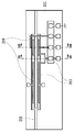
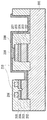
- FIG. 1 is a top view of a high-speed modulator with a surge bypass circuit according to a first embodiment of the present invention. It is the II-II cross section of FIG. 3 is a cross-sectional view taken along the line III-III in FIG. 4 is a cross-sectional view taken along the line IV-IV in FIG. It is a top view of the other high-speed modulator with a surge bypass circuit which concerns on the 1st Embodiment of this invention. It is a top view of the high-speed modulator with a surge bypass circuit according to the second embodiment of the present invention.
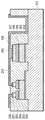
- FIG. 7 is a VII-VII cross section of FIG. 6.
- FIG. 7 is a VIII-VIII cross section of FIG. 6.
- FIG. 7 is a IX-IX cross section of FIG. 6. It is a top view of the other high-speed modulator with a surge bypass circuit which concerns on the 2nd Embodiment of this invention. It is a top view of the other high-speed modulator with a surge bypass circuit which concerns on the 2nd Embodiment of this invention.
- FIG. 12 is a cross section taken along line XII-XII in FIG. 11.
- FIG. 12 is a cross section taken along line XIII-XIII in FIG. 11.
- FIG. 15 is a cross section taken along the line XV-XV in FIG. 14.
- FIG. 15 is a cross section taken along the line XVI-XVI in FIG. 14.
- FIG. 15 is a cross section taken along the line XVII-XVII in FIG. 14.
- the forward voltage ESD having a low ESD failure rate as an ESD countermeasure (reverse voltage ESD) in the pn diode structure device. That is, by connecting a plurality of diodes in series in reverse directions as a countermeasure against ESD, even if a voltage that becomes reverse voltage ESD is applied to the modulation region in the device circuit, Since the forward voltage is applied to any of the plurality of diodes, the electric charge is consumed there. Thereby, the reverse voltage applied to the other diodes including the modulation region can be greatly reduced.
- ESD countermeasure reverse voltage ESD
- thyristor structure such as an npnp or pnpn junction in which pn junctions are connected in series in reverse directions.
- the thyristor structure has a mechanism in which a forward voltage is always applied regardless of which polarity of ESD is applied, unlike the case of a single pn junction, and as a result, there is an effect of increasing ESD resistance. Therefore, it can be said that adding an additional circuit having this thyristor structure in the device is effective as an ESD countermeasure.
- the ground electrode can be used even when ESD occurs thereafter.
- a thyristor structure can be formed between the two. Therefore, ESD tolerance can be improved in the subsequent mounting process.
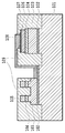
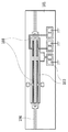
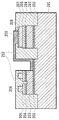
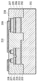
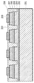
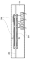
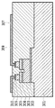
- FIG. 1 shows a top view of a high-speed modulator with a surge bypass circuit according to the first embodiment of the present invention.
- 2 shows a II-II section of FIG. 1
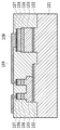
- FIG. 3 shows a III-III section of FIG. 1
- FIG. 4 shows a IV-IV section of FIG.
- the substrate 101 is, for example, an SI type InP (100) substrate as a zinc blende type compound semiconductor crystal.
- An n-type contact layer 102, an n-type cladding layer 103, an undoped core / cladding layer 104, a p-type cladding layer 106, and a p-type contact layer 107 are stacked in this order from the substrate surface by epitaxial growth.
- the core layer of the core / cladding layer 104 has a multi-quantity well structure (PL wavelength: 1. .5) having a period of InGaAsP / InGaAsP in order to efficiently use a refractive index change due to an electro-optic effect with respect to a wavelength of 1.5 ⁇ m band. 4 ⁇ m) was used.
- the composition of the cladding layer of the core / cladding layer 104 is, for example, InP having a refractive index lower than that of the core layer, and the n-type contact layer 102 and the p-type contact layer 107 are lattice-matched to InP and InGaAs having a small energy band gap is used. Using.
- the core and the clad composition only need to have a relative refractive index difference, for example, the core / clad layer 104, the n-type clad layer 103, and the p-type clad layer 106 are made of InGaAlAs having different compositions. It is clear that there is no problem.
- the wavelength is not limited to the 1.5 ⁇ m band.
- the usefulness of the present invention is not lost.
- the conductive p-type cladding layer 106 and the p-type contact layer 107 other than the modulation region and the power supply pad region are removed by dry etching and chemical etching, and then the non-doped cladding layer 105 (here) InP) is deposited by crystal regrowth and backfilled with an organic film 109 such as BCB (for example, FIG. 2).
- the modulation region is a region where the electrode 108 of the Mach-Zehnder interference waveguide is formed, and is a region where a high-frequency signal or a DC voltage is applied to the Mach-Zehnder interference waveguide.
- the core / cladding layer 104 is separated by dry etching using a SiO 2 mask to form a Mach-Zehnder interference waveguide and a plurality of power supply pad installation portions.
- the n-type contact layer 102 and the n-type cladding layer 103 are etched except for the modulation region of the Mach-Zehnder interference waveguide portion and the power supply region where a plurality of power supply pad installation portions are formed.
- the semiconductor is removed by processing to electrically separate the modulation region and the semiconductor below the power feeding region.
- the BCB 109 in a partial region for forming the electrode 108 is removed to expose the n-type contact layer 102 and the p-type contact layer 107.
- the electrode 108 is formed of Au / Ti using a plating method.
- the plurality of power supply pads are formed on the common n-type contact layer 102 and n-type clad layer 103, and a pinip junction is formed between the power supply pads.
- ESD is preferably applied to any power supply pad by first grounding at least one of the power supply pads as shown in FIG. Even if it is made, the connection including the pinip junction between the ground pads becomes possible. In addition, even when there is no power supply pad for ground connection, the order of connecting the Au wires is defined (for example, the power supply pad for the lower n-type clad is finally connected to the wire), so that the utility of the present invention is achieved. Will not be lost.
- each power supply pad electrode is electrically separated, and at least one ground power supply pad is individually formed on each power supply pad. May be.
- the layers are stacked with nip from the substrate surface, but it is clear that the usefulness of the present invention is not lost even if the layers are stacked with the pin from the substrate surface, for example.
- the electrode 108 in the modulation region of the Mach-Zehnder interference waveguide portion, is formed on both of the two arm waveguides, and three power supply pads connected to the modulation electrode are provided.
- the electrode may be formed only on at least one of the p-type contact layers 107 of the arm waveguide, and two power supply pads may be connected to the modulation electrode.
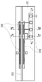
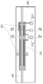
- FIG. 6 is a top view of a high-speed modulator with a surge bypass circuit according to the second embodiment of the present invention.
- 7 shows a VII-VII section of FIG. 6
- FIG. 8 shows a VIII-VIII section of FIG. 6
- FIG. 9 shows a IX-IX section of FIG.
- the semiconductor layer structure is not a general pin structure, but employs a nipn structure capable of forming a light modulator with higher speed and lower loss.
- the structure having a problem in the ESD resistance as compared with the pin structure can also improve the ESD resistance by using the thyristor structure as an additional circuit.
- the substrate 201 is, for example, an SI type InP (100) substrate as a zinc blende type compound semiconductor crystal.
- An n-type contact layer 202, an n-type cladding layer 203, a p-type carrier block layer 204, an undoped core / cladding layer 205, an n-type cladding layer 207, and an n-type contact layer 208 are stacked in this order from the substrate surface by epitaxial growth.
- the core layer of the core-cladding layer 205 has a multi-quantity well structure (PL wavelength: 1..1) having a period of InGaAsP / InGaAsP in order to efficiently use a refractive index change due to an electro-optic effect with respect to a wavelength of 1.5 ⁇ m band. 4 microns).
- the composition of the clad layer of the core / cladding layer 205 was, for example, InP having a refractive index lower than that of the core layer, and the n-type contact layers 202 and 208 used InGaAs having lattice matching with InP and having a small energy band gap.
- the core and clad composition only need to have a relative refractive index difference, there is no problem even if, for example, InGaAlAs or the like having a different composition is used for the core-clad layer 205 and the n-type clad layers 203, 207. Is clear.
- the wavelength is not limited to the 1.5 ⁇ m band.
- the usefulness of the present invention is not lost.
- the conductive n-type cladding layer 207 and the n-type contact layer 208 other than the modulation region and the power supply pad region are removed by dry etching and chemical etching, and then semi-insulating (SI)
- the cladding layer 206 (InP in this case) is deposited by crystal regrowth and backfilled (for example, FIG. 7).
- the Mach-Zehnder interference waveguide and a plurality of power supply pad installation portions are formed by separating the p-type carrier block layer 203 by dry etching using a SiO 2 mask. Thereafter, as shown in FIGS. 7 and 8, the n-type contact layer 202 and the n-type cladding layer 203 are etched except for the modulation region of the Mach-Zehnder interference waveguide portion and the power supply region where a plurality of power supply pad installation portions are formed. The semiconductor is removed by processing to electrically separate the modulation region and the semiconductor below the power feeding region.
- the BCB 210 in a part of the region where the electrode 209 is formed is removed, and the n-type contact layer 202 and the n-type contact layer 208 are exposed and electrically connected thereto.
- the electrode 209 is formed of Au / Ti using vapor deposition and plating.
- the plurality of power supply pads are formed on the common n-type contact layer 202 and the n-type cladding layer 203, and an npinipn junction including a thyristor structure is formed between the power supply pads. In ESD, a junction is formed.
- ESD is preferably applied to any power supply pad by first grounding at least one of the power supply pads as shown in FIG. Even so, a connection including a thyristor structure can be made between the ground pads. Even when the ground connection pad is not provided, the usefulness of the present invention is lost by defining the order in which the Au wires are connected (for example, the power supply pad for the lower n-type cladding is connected last). It will never be.
- each power supply pad electrode is electrically separated, and at least one ground electrode pad is individually formed on each power supply pad. May be.
- npn is stacked in order from the substrate surface.
- the usefulness of the present invention is not lost even if, for example, nnip is stacked in order from the substrate surface. it is obvious.
- the waveguide structure in the modulation region is a ridge-shaped waveguide.
- the usefulness of the present invention is not lost even if the waveguide structure has a high mesa structure, for example, as in the first embodiment. It is.
- the electrode 209 is formed on both of the two arm waveguides, and three power supply pads connected to the modulation electrode are provided.
- the electrode may be formed only on at least one of the n-type contact layers 208 of the arm waveguide, and two power supply pads may be connected to the modulation electrode.
- FIG. 11 shows a top view of another high-speed modulator with a surge bypass circuit according to the second embodiment of the present invention.
- 12 shows a cross section taken along the line XII-XII of FIG. 11
- FIG. 13 shows a cross section taken along the line XIII-XIII of FIG. 11 to 13, instead of providing the power supply pad on the semiconductor layer structure, the power supply pad may be formed so as to be in contact with the substrate 201 exposed by removing the BCB 210. Thereby, it can avoid that the pn junction part of a semiconductor layer structure is destroyed by the pressurization at the time of wire bonding.
- the power supply pad is formed on the opposite side of the Mach-Zehnder interference waveguide with the semiconductor layer structure on the power supply side interposed therebetween, but the power supply pad is formed on the Mach-Zehnder interference waveguide and the semiconductor on the power supply side. It may be formed between the layer structure.
- the configuration in which the power supply pad is formed not directly on the semiconductor layer structure but directly on the substrate 201 has been described by taking the second embodiment as an example.
- the same effect can be obtained by forming the power supply pad directly on the substrate 101 in the first embodiment. It goes without saying that can be obtained.
Landscapes
- Physics & Mathematics (AREA)
- Nonlinear Science (AREA)
- General Physics & Mathematics (AREA)
- Optics & Photonics (AREA)
- Optical Modulation, Optical Deflection, Nonlinear Optics, Optical Demodulation, Optical Logic Elements (AREA)
Abstract
Description
図1に、本発明の第1の実施形態に係るサージバイパス回路付高速変調器の上面図を示す。図2に図1のII-II断面を示し、図3に図1のIII-III断面を示し、図4に図1のIV-IV断面を示す。
図6に、本発明の第2の実施形態に係るサージバイパス回路付高速変調器の上面図を示す。図7に図6のVII-VII断面を示し、図8に図6のVIII-VIII断面を示し、図9に図6のIX-IX断面を示す。実施形態1との差異は半導体層構造が一般的なpin構造ではなく、より高速・低損失な光変調器を構成可能なnipn構造を採用している点である。前述のとおり、pin構造に比べてESD耐性に課題を有する当該構造もサイリスタ構造を付加回路として用いることでESD耐性を向上させることができる。
102、202、208 n型コンタクト層
103、203、207 n型クラッド層
104、205 ノンドープのコア・クラッド層
105 ノンドープのクラッド層
106 p型クラッド層
107 p型コンタクト層
108、209 電極
109、210 BCB
204 p型キャリアブロック層
206 SIクラッド層
301 基板
302 n型コンタクト層
303 n型クラッド層
304 p型キャリアブロック層
305 ノンドープのコア・クラッド層
306 SIクラッド層
307 電極
308 BCB
Claims (8)
- 半絶縁性基板上に少なくともn型又はp型クラッド層である第1のクラッド層、ノンドープのコア及びクラッド層、p型又はn型クラッド層である第2のクラッド層の順で積層されたpin接合を有する積層構造に光導波路が形成された半導体光変調素子であって、
前記積層構造上に形成された給電電極設置部と、
前記電極設置部上に形成された少なくとも2本の給電電極と、
を備え、少なくとも2本の前記給電電極は前記光導波路上に設置された変調電極に接続され、
前記給電電極設置部は、前記給電電極間が電気的に分離されるように前記給電電極毎に前記積層構造の前記第2のクラッド層と前記ノンドープのコア及びクラッド層とが電気的に分離され、かつ、少なくとも2本の前記給電電極間は、前記積層構造の前記第1のクラッド層を介して互いに導通され、
前記光導波路と前記給電電極設置部とは前記積層構造に関して電気的に分離されていることを特徴とする半導体光変調素子。 - 半絶縁性基板上に少なくともn型又はp型クラッド層である第1のクラッド層、ノンドープのコア及びクラッド層、p型又はn型クラッド層である第2のクラッド層の順で積層されたpin接合を有する積層構造に光導波路が形成された半導体光変調素子であって、
前記積層構造上に形成された給電電極設置部と、
前記給電電極設置部上に形成された少なくとも3本の給電電極と、
を備え、前記給電電極の少なくとも2本は前記光導波路上に設置された変調電極に接続され、前記給電電極の少なくとも1本は接地され、
前記給電電極設置部は、前記給電電極間が電気的に分離されるように前記給電電極毎に前記積層構造の前記第2のクラッド層と前記ノンドープのコア及びクラッド層とが電気的に分離され、かつ、少なくとも前記変調電極に接続された前記給電電極と接地された前記給電電極との間は、前記積層構造の前記第1のクラッド層を介して互いに導通され、
前記光導波路と前記給電電極設置部とは前記積層構造に関して電気的に分離されていることを特徴とする半導体光変調素子。 - 半絶縁性基板上に少なくともn型又はp型クラッド層である第1のクラッド層、ノンドープのコア及びクラッド層、p型又はn型キャリアブロック層、n型又はp型クラッド層である第2のクラッド層の順で積層されたnipn接合又はpinp接合を有する積層構造に光導波路が形成された半導体光変調素子であって、
前記積層構造上に形成された給電電極設置部と、
前記給電電極設置部上に形成された少なくとも2本の給電電極と、
を備え、少なくとも2本の前記給電電極は前記光導波路上に設置された変調電極に接続され、
前記給電電極設置部は、前記給電電極間が電気的に分離されるように前記給電電極毎に前記積層構造の前記第2のクラッド層と前記p型又はn型キャリアブロック層と前記ノンドープのコア及びクラッド層とが電気的に分離され、かつ、少なくとも2本の前記給電電極間は、前記積層構造の前記第1のクラッド層を介して互いに導通され、
前記光導波路と前記給電電極設置部とは前記積層構造に関して電気的に分離されていることを特徴とする半導体光変調素子。 - 半絶縁性基板上に少なくともn型又はp型クラッド層である第1のクラッド層、ノンドープのコア及びクラッド層、p型又はn型キャリアブロック層、n型又はp型クラッド層である第2のクラッド層の順に積層されたnipn接合又はpinp接合を有する積層構造に光導波路が形成された半導体光変調素子であって、
前記積層構造上に形成された給電電極設置部と、
前記給電電極設置部上に形成された少なくとも3本の給電電極と、
を備え、前記給電電極の少なくとも2本は前記光導波路上に設置された変調電極に接続され、前記給電電極の少なくとも1本は接地され、
前記給電電極設置部は、前記給電電極間が電気的に分離されるように前記給電電極毎に前記積層構造の前記第2のクラッド層と前記p型又はn型キャリアブロック層と前記ノンドープのコア及びクラッド層とが電気的に分離され、かつ、前記変調電極に接続された前記給電電極と接地された前記給電電極との間は、前記積層構造の前記第2のクラッド層を介して互いに導通され、
前記光導波路と前記給電電極設置部とは前記積層構造に関して電気的に分離されていることを特徴とする半導体光変調素子。 - 前記給電電極は、前記半絶縁性基板に接するように形成された給電パッドを有することを特徴とする請求項1乃至4のいずれかに記載の半導体光変調素子。
- 前記変調電極に接続された給電電極の各々は、接地された、異なる少なくとも1つの前記給電電極に前記第1のクラッド層を介して導通されていることを特徴とする請求項2又は4に記載の半導体光変調素子。
- 前記光導波路は、マッハ・ツェンダ型光干渉計を構成していることを特徴とする請求項1乃至6のいずれかに記載の半導体光変調素子。
- 前記変調電極は、容量装荷型の進行波電極構造を有していることを特徴とする請求項1乃至7のいずれかに記載の半導体光変調素子。
Priority Applications (5)
| Application Number | Priority Date | Filing Date | Title |
|---|---|---|---|
| US16/332,740 US11126058B1 (en) | 2016-09-13 | 2017-09-13 | Semiconductor optical modulation element |
| EP17850914.7A EP3514616B1 (en) | 2016-09-13 | 2017-09-13 | Semiconductor optical modulation element |
| CA3036468A CA3036468C (en) | 2016-09-13 | 2017-09-13 | Semiconductor optical modulation element |
| CN201780056209.1A CN109690392B (zh) | 2016-09-13 | 2017-09-13 | 半导体光调制元件 |
| JP2018539743A JP6592610B2 (ja) | 2016-09-13 | 2017-09-13 | 半導体光変調素子 |
Applications Claiming Priority (2)
| Application Number | Priority Date | Filing Date | Title |
|---|---|---|---|
| JP2016-178905 | 2016-09-13 | ||
| JP2016178905 | 2016-09-13 |
Publications (1)
| Publication Number | Publication Date |
|---|---|
| WO2018052013A1 true WO2018052013A1 (ja) | 2018-03-22 |
Family
ID=61619546
Family Applications (1)
| Application Number | Title | Priority Date | Filing Date |
|---|---|---|---|
| PCT/JP2017/033014 Ceased WO2018052013A1 (ja) | 2016-09-13 | 2017-09-13 | 半導体光変調素子 |
Country Status (7)
| Country | Link |
|---|---|
| US (1) | US11126058B1 (ja) |
| EP (1) | EP3514616B1 (ja) |
| JP (1) | JP6592610B2 (ja) |
| CN (1) | CN109690392B (ja) |
| CA (1) | CA3036468C (ja) |
| TW (1) | TWI632413B (ja) |
| WO (1) | WO2018052013A1 (ja) |
Cited By (2)
| Publication number | Priority date | Publication date | Assignee | Title |
|---|---|---|---|---|
| JP2020052361A (ja) * | 2018-09-28 | 2020-04-02 | 住友電気工業株式会社 | 半導体装置およびその製造方法 |
| JP2021033042A (ja) * | 2019-08-23 | 2021-03-01 | 住友電気工業株式会社 | 光変調器 |
Families Citing this family (5)
| Publication number | Priority date | Publication date | Assignee | Title |
|---|---|---|---|---|
| WO2020245618A2 (zh) * | 2019-05-20 | 2020-12-10 | 华为技术(美国)有限公司 | 种电光调制器、光器件及光模块 |
| WO2021013960A1 (en) * | 2019-07-24 | 2021-01-28 | Rockley Photonics Limited | Electro-optic modulator |
| US12245459B2 (en) * | 2019-08-23 | 2025-03-04 | Sharp Kabushiki Kaisha | Light-emitting device including a light-emitting diode and a protective diode and display device |
| US20220066280A1 (en) * | 2020-08-25 | 2022-03-03 | Sumitomo Electric Industries, Ltd. | Optical modulator |
| JP7632101B2 (ja) | 2021-06-11 | 2025-02-19 | 住友電気工業株式会社 | 光変調器及び光変調器の製造方法 |
Citations (6)
| Publication number | Priority date | Publication date | Assignee | Title |
|---|---|---|---|---|
| JPS5919389A (ja) * | 1982-07-24 | 1984-01-31 | Fujitsu Ltd | 半導体装置 |
| US20050018730A1 (en) * | 2003-07-25 | 2005-01-27 | The University Of Connecticut And Opel, Inc. | Semiconductor laser array device employing modulation doped quantum well structures |
| JP2005217381A (ja) * | 2004-02-02 | 2005-08-11 | Sony Corp | 半導体発光装置とその製造方法 |
| JP2007512689A (ja) * | 2003-11-28 | 2007-05-17 | オスラム オプト セミコンダクターズ ゲゼルシャフト ミット ベシュレンクテル ハフツング | 保護ダイオードを備えた発光半導体素子 |
| JP2010287604A (ja) * | 2009-06-09 | 2010-12-24 | Nec Corp | 導波路型光素子及びその製造方法 |
| JP2011197343A (ja) * | 2010-03-19 | 2011-10-06 | Nippon Telegr & Teleph Corp <Ntt> | サージ保護機能内蔵型半導体光変調器及びその製造方法 |
Family Cites Families (6)
| Publication number | Priority date | Publication date | Assignee | Title |
|---|---|---|---|---|
| JP2754957B2 (ja) * | 1991-07-10 | 1998-05-20 | 日本電気株式会社 | 半導体光制御素子およびその製造方法 |
| US5914501A (en) | 1998-08-27 | 1999-06-22 | Hewlett-Packard Company | Light emitting diode assembly having integrated electrostatic discharge protection |
| JP4047785B2 (ja) | 2003-09-24 | 2008-02-13 | Nttエレクトロニクス株式会社 | 半導体光電子導波路 |
| US7462884B2 (en) * | 2005-10-31 | 2008-12-09 | Nichia Corporation | Nitride semiconductor device |
| JP2011191343A (ja) * | 2010-03-11 | 2011-09-29 | Seiko Epson Corp | 表示シート、表示装置および電子機器 |
| JP5705786B2 (ja) | 2012-05-24 | 2015-04-22 | 日本電信電話株式会社 | 半導体光位相変調器 |
-
2017
- 2017-09-13 JP JP2018539743A patent/JP6592610B2/ja active Active
- 2017-09-13 TW TW106131436A patent/TWI632413B/zh active
- 2017-09-13 US US16/332,740 patent/US11126058B1/en active Active
- 2017-09-13 CN CN201780056209.1A patent/CN109690392B/zh active Active
- 2017-09-13 EP EP17850914.7A patent/EP3514616B1/en active Active
- 2017-09-13 CA CA3036468A patent/CA3036468C/en active Active
- 2017-09-13 WO PCT/JP2017/033014 patent/WO2018052013A1/ja not_active Ceased
Patent Citations (6)
| Publication number | Priority date | Publication date | Assignee | Title |
|---|---|---|---|---|
| JPS5919389A (ja) * | 1982-07-24 | 1984-01-31 | Fujitsu Ltd | 半導体装置 |
| US20050018730A1 (en) * | 2003-07-25 | 2005-01-27 | The University Of Connecticut And Opel, Inc. | Semiconductor laser array device employing modulation doped quantum well structures |
| JP2007512689A (ja) * | 2003-11-28 | 2007-05-17 | オスラム オプト セミコンダクターズ ゲゼルシャフト ミット ベシュレンクテル ハフツング | 保護ダイオードを備えた発光半導体素子 |
| JP2005217381A (ja) * | 2004-02-02 | 2005-08-11 | Sony Corp | 半導体発光装置とその製造方法 |
| JP2010287604A (ja) * | 2009-06-09 | 2010-12-24 | Nec Corp | 導波路型光素子及びその製造方法 |
| JP2011197343A (ja) * | 2010-03-19 | 2011-10-06 | Nippon Telegr & Teleph Corp <Ntt> | サージ保護機能内蔵型半導体光変調器及びその製造方法 |
Non-Patent Citations (1)
| Title |
|---|
| See also references of EP3514616A4 * |
Cited By (4)
| Publication number | Priority date | Publication date | Assignee | Title |
|---|---|---|---|---|
| JP2020052361A (ja) * | 2018-09-28 | 2020-04-02 | 住友電気工業株式会社 | 半導体装置およびその製造方法 |
| JP7110879B2 (ja) | 2018-09-28 | 2022-08-02 | 住友電気工業株式会社 | 半導体装置およびその製造方法 |
| JP2021033042A (ja) * | 2019-08-23 | 2021-03-01 | 住友電気工業株式会社 | 光変調器 |
| JP7404711B2 (ja) | 2019-08-23 | 2023-12-26 | 住友電気工業株式会社 | 光変調器 |
Also Published As
| Publication number | Publication date |
|---|---|
| CA3036468C (en) | 2022-05-03 |
| EP3514616A1 (en) | 2019-07-24 |
| US20210294176A1 (en) | 2021-09-23 |
| JP6592610B2 (ja) | 2019-10-16 |
| EP3514616B1 (en) | 2021-08-04 |
| JPWO2018052013A1 (ja) | 2019-02-14 |
| CN109690392A (zh) | 2019-04-26 |
| TW201825971A (zh) | 2018-07-16 |
| EP3514616A4 (en) | 2020-06-03 |
| US11126058B1 (en) | 2021-09-21 |
| CN109690392B (zh) | 2022-05-03 |
| TWI632413B (zh) | 2018-08-11 |
| CA3036468A1 (en) | 2018-03-22 |
Similar Documents
| Publication | Publication Date | Title |
|---|---|---|
| JP6592610B2 (ja) | 半導体光変調素子 | |
| EP3306381B1 (en) | Semiconductor optical modulation element | |
| CN101529313B (zh) | 半导体光调制器 | |
| US9280004B2 (en) | Method for manufacturing semiconductor modulator and semiconductor modulator | |
| US20240170914A1 (en) | Semiconductor sub-assemblies for emitting modulated light | |
| US20220066280A1 (en) | Optical modulator | |
| JP2024531669A (ja) | 電気光学変調器 | |
| US11300850B2 (en) | Mach-Zehnder modulator | |
| CN112415787A (zh) | 光调制器 | |
| US20200192132A1 (en) | Optical modulator | |
| JP7758211B2 (ja) | 光半導体装置、光半導体装置を備えた光伝送装置及び光伝送装置の製造方法 | |
| US20230352911A1 (en) | Semiconductor optical device | |
| EP3739635A1 (en) | A device comprising an active component and associated electrodes and a method of manufacturing such device | |
| US20260126679A1 (en) | Optical semiconductor device | |
| CN118511113A (zh) | 电光调制器 | |
| JP2001183612A (ja) | 光変調素子 | |
| JP2004363268A (ja) | 光半導体装置 |
Legal Events
| Date | Code | Title | Description |
|---|---|---|---|
| ENP | Entry into the national phase |
Ref document number: 2018539743 Country of ref document: JP Kind code of ref document: A |
|
| 121 | Ep: the epo has been informed by wipo that ep was designated in this application |
Ref document number: 17850914 Country of ref document: EP Kind code of ref document: A1 |
|
| ENP | Entry into the national phase |
Ref document number: 3036468 Country of ref document: CA |
|
| NENP | Non-entry into the national phase |
Ref country code: DE |
|
| ENP | Entry into the national phase |
Ref document number: 2017850914 Country of ref document: EP Effective date: 20190415 |