WO2018055902A1 - Dispositif d'affichage et dispositif électronique - Google Patents
Dispositif d'affichage et dispositif électronique Download PDFInfo
- Publication number
- WO2018055902A1 WO2018055902A1 PCT/JP2017/027160 JP2017027160W WO2018055902A1 WO 2018055902 A1 WO2018055902 A1 WO 2018055902A1 JP 2017027160 W JP2017027160 W JP 2017027160W WO 2018055902 A1 WO2018055902 A1 WO 2018055902A1
- Authority
- WO
- WIPO (PCT)
- Prior art keywords
- wiring
- wiring layer
- layer
- light emitting
- pixel
- Prior art date
- Legal status (The legal status is an assumption and is not a legal conclusion. Google has not performed a legal analysis and makes no representation as to the accuracy of the status listed.)
- Ceased
Links
Images


Classifications
-
- G—PHYSICS
- G09—EDUCATION; CRYPTOGRAPHY; DISPLAY; ADVERTISING; SEALS
- G09G—ARRANGEMENTS OR CIRCUITS FOR CONTROL OF INDICATING DEVICES USING STATIC MEANS TO PRESENT VARIABLE INFORMATION
- G09G3/00—Control arrangements or circuits, of interest only in connection with visual indicators other than cathode-ray tubes
- G09G3/20—Control arrangements or circuits, of interest only in connection with visual indicators other than cathode-ray tubes for presentation of an assembly of a number of characters, e.g. a page, by composing the assembly by combination of individual elements arranged in a matrix no fixed position being assigned to or needed to be assigned to the individual characters or partial characters
- G09G3/22—Control arrangements or circuits, of interest only in connection with visual indicators other than cathode-ray tubes for presentation of an assembly of a number of characters, e.g. a page, by composing the assembly by combination of individual elements arranged in a matrix no fixed position being assigned to or needed to be assigned to the individual characters or partial characters using controlled light sources
- G09G3/30—Control arrangements or circuits, of interest only in connection with visual indicators other than cathode-ray tubes for presentation of an assembly of a number of characters, e.g. a page, by composing the assembly by combination of individual elements arranged in a matrix no fixed position being assigned to or needed to be assigned to the individual characters or partial characters using controlled light sources using electroluminescent panels
- G09G3/32—Control arrangements or circuits, of interest only in connection with visual indicators other than cathode-ray tubes for presentation of an assembly of a number of characters, e.g. a page, by composing the assembly by combination of individual elements arranged in a matrix no fixed position being assigned to or needed to be assigned to the individual characters or partial characters using controlled light sources using electroluminescent panels semiconductive, e.g. using light-emitting diodes [LED]
- G09G3/3208—Control arrangements or circuits, of interest only in connection with visual indicators other than cathode-ray tubes for presentation of an assembly of a number of characters, e.g. a page, by composing the assembly by combination of individual elements arranged in a matrix no fixed position being assigned to or needed to be assigned to the individual characters or partial characters using controlled light sources using electroluminescent panels semiconductive, e.g. using light-emitting diodes [LED] organic, e.g. using organic light-emitting diodes [OLED]
- G09G3/3266—Details of drivers for scan electrodes
-
- H—ELECTRICITY
- H10—SEMICONDUCTOR DEVICES; ELECTRIC SOLID-STATE DEVICES NOT OTHERWISE PROVIDED FOR
- H10K—ORGANIC ELECTRIC SOLID-STATE DEVICES
- H10K59/00—Integrated devices, or assemblies of multiple devices, comprising at least one organic light-emitting element covered by group H10K50/00
- H10K59/10—OLED displays
- H10K59/12—Active-matrix OLED [AMOLED] displays
-
- H—ELECTRICITY
- H10—SEMICONDUCTOR DEVICES; ELECTRIC SOLID-STATE DEVICES NOT OTHERWISE PROVIDED FOR
- H10D—INORGANIC ELECTRIC SEMICONDUCTOR DEVICES
- H10D86/00—Integrated devices formed in or on insulating or conducting substrates, e.g. formed in silicon-on-insulator [SOI] substrates or on stainless steel or glass substrates
- H10D86/40—Integrated devices formed in or on insulating or conducting substrates, e.g. formed in silicon-on-insulator [SOI] substrates or on stainless steel or glass substrates characterised by multiple TFTs
- H10D86/441—Interconnections, e.g. scanning lines
-
- H—ELECTRICITY
- H10—SEMICONDUCTOR DEVICES; ELECTRIC SOLID-STATE DEVICES NOT OTHERWISE PROVIDED FOR
- H10D—INORGANIC ELECTRIC SEMICONDUCTOR DEVICES
- H10D86/00—Integrated devices formed in or on insulating or conducting substrates, e.g. formed in silicon-on-insulator [SOI] substrates or on stainless steel or glass substrates
- H10D86/40—Integrated devices formed in or on insulating or conducting substrates, e.g. formed in silicon-on-insulator [SOI] substrates or on stainless steel or glass substrates characterised by multiple TFTs
- H10D86/481—Integrated devices formed in or on insulating or conducting substrates, e.g. formed in silicon-on-insulator [SOI] substrates or on stainless steel or glass substrates characterised by multiple TFTs integrated with passive devices, e.g. auxiliary capacitors
-
- H—ELECTRICITY
- H10—SEMICONDUCTOR DEVICES; ELECTRIC SOLID-STATE DEVICES NOT OTHERWISE PROVIDED FOR
- H10D—INORGANIC ELECTRIC SEMICONDUCTOR DEVICES
- H10D86/00—Integrated devices formed in or on insulating or conducting substrates, e.g. formed in silicon-on-insulator [SOI] substrates or on stainless steel or glass substrates
- H10D86/40—Integrated devices formed in or on insulating or conducting substrates, e.g. formed in silicon-on-insulator [SOI] substrates or on stainless steel or glass substrates characterised by multiple TFTs
- H10D86/60—Integrated devices formed in or on insulating or conducting substrates, e.g. formed in silicon-on-insulator [SOI] substrates or on stainless steel or glass substrates characterised by multiple TFTs wherein the TFTs are in active matrices
-
- H—ELECTRICITY
- H10—SEMICONDUCTOR DEVICES; ELECTRIC SOLID-STATE DEVICES NOT OTHERWISE PROVIDED FOR
- H10K—ORGANIC ELECTRIC SOLID-STATE DEVICES
- H10K50/00—Organic light-emitting devices
- H10K50/10—OLEDs or polymer light-emitting diodes [PLED]
- H10K50/11—OLEDs or polymer light-emitting diodes [PLED] characterised by the electroluminescent [EL] layers
- H10K50/125—OLEDs or polymer light-emitting diodes [PLED] characterised by the electroluminescent [EL] layers specially adapted for multicolour light emission, e.g. for emitting white light
-
- H—ELECTRICITY
- H10—SEMICONDUCTOR DEVICES; ELECTRIC SOLID-STATE DEVICES NOT OTHERWISE PROVIDED FOR
- H10K—ORGANIC ELECTRIC SOLID-STATE DEVICES
- H10K59/00—Integrated devices, or assemblies of multiple devices, comprising at least one organic light-emitting element covered by group H10K50/00
- H10K59/10—OLED displays
- H10K59/12—Active-matrix OLED [AMOLED] displays
- H10K59/121—Active-matrix OLED [AMOLED] displays characterised by the geometry or disposition of pixel elements
- H10K59/1213—Active-matrix OLED [AMOLED] displays characterised by the geometry or disposition of pixel elements the pixel elements being TFTs
-
- H—ELECTRICITY
- H10—SEMICONDUCTOR DEVICES; ELECTRIC SOLID-STATE DEVICES NOT OTHERWISE PROVIDED FOR
- H10K—ORGANIC ELECTRIC SOLID-STATE DEVICES
- H10K59/00—Integrated devices, or assemblies of multiple devices, comprising at least one organic light-emitting element covered by group H10K50/00
- H10K59/10—OLED displays
- H10K59/12—Active-matrix OLED [AMOLED] displays
- H10K59/121—Active-matrix OLED [AMOLED] displays characterised by the geometry or disposition of pixel elements
- H10K59/1216—Active-matrix OLED [AMOLED] displays characterised by the geometry or disposition of pixel elements the pixel elements being capacitors
-
- H—ELECTRICITY
- H10—SEMICONDUCTOR DEVICES; ELECTRIC SOLID-STATE DEVICES NOT OTHERWISE PROVIDED FOR
- H10K—ORGANIC ELECTRIC SOLID-STATE DEVICES
- H10K59/00—Integrated devices, or assemblies of multiple devices, comprising at least one organic light-emitting element covered by group H10K50/00
- H10K59/10—OLED displays
- H10K59/12—Active-matrix OLED [AMOLED] displays
- H10K59/122—Pixel-defining structures or layers, e.g. banks
-
- H—ELECTRICITY
- H10—SEMICONDUCTOR DEVICES; ELECTRIC SOLID-STATE DEVICES NOT OTHERWISE PROVIDED FOR
- H10K—ORGANIC ELECTRIC SOLID-STATE DEVICES
- H10K59/00—Integrated devices, or assemblies of multiple devices, comprising at least one organic light-emitting element covered by group H10K50/00
- H10K59/10—OLED displays
- H10K59/12—Active-matrix OLED [AMOLED] displays
- H10K59/131—Interconnections, e.g. wiring lines or terminals
-
- H—ELECTRICITY
- H10—SEMICONDUCTOR DEVICES; ELECTRIC SOLID-STATE DEVICES NOT OTHERWISE PROVIDED FOR
- H10K—ORGANIC ELECTRIC SOLID-STATE DEVICES
- H10K59/00—Integrated devices, or assemblies of multiple devices, comprising at least one organic light-emitting element covered by group H10K50/00
- H10K59/60—OLEDs integrated with inorganic light-sensitive elements, e.g. with inorganic solar cells or inorganic photodiodes
- H10K59/65—OLEDs integrated with inorganic image sensors
-
- G—PHYSICS
- G09—EDUCATION; CRYPTOGRAPHY; DISPLAY; ADVERTISING; SEALS
- G09G—ARRANGEMENTS OR CIRCUITS FOR CONTROL OF INDICATING DEVICES USING STATIC MEANS TO PRESENT VARIABLE INFORMATION
- G09G2300/00—Aspects of the constitution of display devices
- G09G2300/04—Structural and physical details of display devices
- G09G2300/0421—Structural details of the set of electrodes
- G09G2300/0426—Layout of electrodes and connections
-
- G—PHYSICS
- G09—EDUCATION; CRYPTOGRAPHY; DISPLAY; ADVERTISING; SEALS
- G09G—ARRANGEMENTS OR CIRCUITS FOR CONTROL OF INDICATING DEVICES USING STATIC MEANS TO PRESENT VARIABLE INFORMATION
- G09G2320/00—Control of display operating conditions
- G09G2320/02—Improving the quality of display appearance
- G09G2320/0233—Improving the luminance or brightness uniformity across the screen
-
- G—PHYSICS
- G09—EDUCATION; CRYPTOGRAPHY; DISPLAY; ADVERTISING; SEALS
- G09G—ARRANGEMENTS OR CIRCUITS FOR CONTROL OF INDICATING DEVICES USING STATIC MEANS TO PRESENT VARIABLE INFORMATION
- G09G3/00—Control arrangements or circuits, of interest only in connection with visual indicators other than cathode-ray tubes
- G09G3/20—Control arrangements or circuits, of interest only in connection with visual indicators other than cathode-ray tubes for presentation of an assembly of a number of characters, e.g. a page, by composing the assembly by combination of individual elements arranged in a matrix no fixed position being assigned to or needed to be assigned to the individual characters or partial characters
- G09G3/22—Control arrangements or circuits, of interest only in connection with visual indicators other than cathode-ray tubes for presentation of an assembly of a number of characters, e.g. a page, by composing the assembly by combination of individual elements arranged in a matrix no fixed position being assigned to or needed to be assigned to the individual characters or partial characters using controlled light sources
- G09G3/30—Control arrangements or circuits, of interest only in connection with visual indicators other than cathode-ray tubes for presentation of an assembly of a number of characters, e.g. a page, by composing the assembly by combination of individual elements arranged in a matrix no fixed position being assigned to or needed to be assigned to the individual characters or partial characters using controlled light sources using electroluminescent panels
- G09G3/32—Control arrangements or circuits, of interest only in connection with visual indicators other than cathode-ray tubes for presentation of an assembly of a number of characters, e.g. a page, by composing the assembly by combination of individual elements arranged in a matrix no fixed position being assigned to or needed to be assigned to the individual characters or partial characters using controlled light sources using electroluminescent panels semiconductive, e.g. using light-emitting diodes [LED]
- G09G3/3208—Control arrangements or circuits, of interest only in connection with visual indicators other than cathode-ray tubes for presentation of an assembly of a number of characters, e.g. a page, by composing the assembly by combination of individual elements arranged in a matrix no fixed position being assigned to or needed to be assigned to the individual characters or partial characters using controlled light sources using electroluminescent panels semiconductive, e.g. using light-emitting diodes [LED] organic, e.g. using organic light-emitting diodes [OLED]
- G09G3/3225—Control arrangements or circuits, of interest only in connection with visual indicators other than cathode-ray tubes for presentation of an assembly of a number of characters, e.g. a page, by composing the assembly by combination of individual elements arranged in a matrix no fixed position being assigned to or needed to be assigned to the individual characters or partial characters using controlled light sources using electroluminescent panels semiconductive, e.g. using light-emitting diodes [LED] organic, e.g. using organic light-emitting diodes [OLED] using an active matrix
- G09G3/3233—Control arrangements or circuits, of interest only in connection with visual indicators other than cathode-ray tubes for presentation of an assembly of a number of characters, e.g. a page, by composing the assembly by combination of individual elements arranged in a matrix no fixed position being assigned to or needed to be assigned to the individual characters or partial characters using controlled light sources using electroluminescent panels semiconductive, e.g. using light-emitting diodes [LED] organic, e.g. using organic light-emitting diodes [OLED] using an active matrix with pixel circuitry controlling the current through the light-emitting element
-
- H—ELECTRICITY
- H10—SEMICONDUCTOR DEVICES; ELECTRIC SOLID-STATE DEVICES NOT OTHERWISE PROVIDED FOR
- H10K—ORGANIC ELECTRIC SOLID-STATE DEVICES
- H10K59/00—Integrated devices, or assemblies of multiple devices, comprising at least one organic light-emitting element covered by group H10K50/00
- H10K59/10—OLED displays
- H10K59/12—Active-matrix OLED [AMOLED] displays
- H10K59/123—Connection of the pixel electrodes to the thin film transistors [TFT]
-
- H—ELECTRICITY
- H10—SEMICONDUCTOR DEVICES; ELECTRIC SOLID-STATE DEVICES NOT OTHERWISE PROVIDED FOR
- H10K—ORGANIC ELECTRIC SOLID-STATE DEVICES
- H10K59/00—Integrated devices, or assemblies of multiple devices, comprising at least one organic light-emitting element covered by group H10K50/00
- H10K59/30—Devices specially adapted for multicolour light emission
- H10K59/35—Devices specially adapted for multicolour light emission comprising red-green-blue [RGB] subpixels
- H10K59/351—Devices specially adapted for multicolour light emission comprising red-green-blue [RGB] subpixels comprising more than three subpixels, e.g. red-green-blue-white [RGBW]
Definitions
- This disclosure relates to a display device and an electronic device.
- the display device In a display device driven by a so-called active matrix method, the display device extends along the horizontal direction of the display surface (hereinafter also referred to as the horizontal direction) and is arranged in a plurality in the vertical direction of the display surface (hereinafter also referred to as the vertical direction).
- the horizontal direction For driving the light emitting element and the light emitting element at positions corresponding to the intersections of the scanning line and the data lines (signal lines) extending in the vertical direction and arranged in the horizontal direction.
- a pixel circuit including the driving circuit is provided.
- One pixel circuit corresponds to one pixel or subpixel.
- an active element a transistor or the like
- light emission of the light emitting element in the pixel circuit is performed. Is controlled.
- a display device driven by the active matrix method for example, a display device using an organic light emitting diode (OLED) as a light emitting element (hereinafter also referred to as an organic EL (electroluminescence) display device) has been developed.
- OLED organic light emitting diode
- an organic EL electroluminescence
- a display device for example, in order to realize higher-definition display or to be mounted on a relatively small electronic device such as a wearable device, it is required to further reduce the pixel size.
- the layout of the pixel circuit is also miniaturized, which may cause the following problems. That is, the luminance uniformity is deteriorated due to noise interference between the electrodes due to the increase in parasitic capacitance between the wires, the luminance uniformity is deteriorated due to the noise resistance deterioration due to the compression of the electrode area of the capacitive element, and the pixel wiring is densely arranged.
- the present disclosure proposes a new and improved display device and electronic apparatus that can further improve reliability.
- a pixel unit configured by arranging a plurality of pixel circuits each including a light emitting element and a driving circuit for driving the light emitting element in a matrix, and a wiring connected to each of the pixel circuits A scanning line extending in a first direction corresponding to each row of the plurality of pixel circuits, and a wiring connected to each of the pixel circuits, each of the plurality of pixel circuits A signal line extending in a second direction orthogonal to the first direction corresponding to a column, and provided for one pixel circuit among the scanning line and the signal line
- the display device in which the larger number is located in a lower wiring layer, and the electrode of the capacitor element included in the drive circuit is located in the wiring layer provided with either the scanning line or the signal line Is provided.
- a display device that performs display based on a video signal
- the display device includes a pixel circuit including a light emitting element and a drive circuit for driving the light emitting element in a matrix.
- the larger number provided for one pixel circuit is located in a lower wiring layer, and the electrodes of the capacitor elements included in the driving circuit are provided. Any one of the scanning line and the signal line is provided. Situated in that the wiring layer, the electronic device is provided.
- a lower wiring layer is provided. Formed. Therefore, the wiring pattern in the upper wiring layer can be made relatively sparse.
- the electrode of the capacitor element included in the pixel circuit is formed in a wiring layer provided with one of the two types of wiring. In other words, since the electrode of the capacitor element can be provided in the wiring layer having a relatively sparse wiring pattern, the degree of freedom of arrangement of the electrode is improved and the area of the electrode can be sufficiently secured. Therefore, it is possible to solve problems caused by the relatively dense wiring pattern, problems caused by insufficiently securing the electrode area of the capacitor, and the like. Therefore, a display device with higher reliability can be realized.
- the reliability can be further improved.
- the above effects are not necessarily limited, and any of the effects shown in the present specification, or other effects that can be grasped from the present specification, together with the above effects or instead of the above effects. May be played.
- FIG. 2 is a schematic diagram illustrating the configuration of a pixel unit, a scanning unit, and a selection unit illustrated in FIG. 1 in more detail.
- FIG. 3 is a schematic diagram illustrating a configuration example of a pixel circuit illustrated in FIG. 2. It is a figure for demonstrating operation
- FIG. 8 is a diagram for comparison with the layout shown in FIG.
- FIG. 7 is a diagram showing an example of a layout when V signal lines are formed. It is a figure for demonstrating the other example of the layout of the wiring layer which concerns on this embodiment.
- FIG. 10 is a diagram for comparison with the layout shown in FIG. 9, and different wirings from the present embodiment when H scanning lines and V signal lines are formed in the first wiring layer, the second wiring layer, and the third wiring layer. It is a figure which shows one layout example at the time of forming the H scanning line and V signal line in the layer.
- the display device is an organic EL display device
- the present disclosure is not limited to this example, and the display device that is the subject of the present disclosure may be various display devices as long as the display device is driven by an active matrix driving method.
- FIG. 1 is a schematic diagram illustrating an overall configuration of a display device according to the present embodiment.
- FIG. 2 is a schematic diagram illustrating the configuration of the pixel unit, the scanning unit, and the selection unit illustrated in FIG. 1 in more detail.
- the display device 1 includes a pixel unit 20, a scanning unit 30, and a selection unit 40 arranged on a display panel 10.
- the pixel unit 20 includes a plurality of pixel circuits 210 arranged in a matrix. Note that although the pixel circuit 210 is described for convenience, the “pixel circuit 210” illustrated in FIG. 2 indicates a portion excluding the wiring layer of the pixel circuit 210, and actually, “pixel circuit 210” illustrated in FIG.
- the pixel circuit 210 may be configured by connecting each wiring (wiring extending from the scanning unit 30 and the selection unit 40 described later, a power supply line 332, and the like) to the pixel circuit 210 ”.
- these wirings can be provided in common for the plurality of pixel circuits 210, they can also form part of the pixel circuit 210. Therefore, in FIG. For the sake of convenience, the portion excluding “” is illustrated as a pixel circuit 210. In this specification, in the case where the pixel circuit 210 is described, only the portion excluding the wiring layer may be pointed out for convenience.
- One pixel circuit 210 corresponds to one subpixel.
- the display device 1 is a display device capable of color display, and one pixel as a unit for forming a color image is composed of a plurality of sub-pixels.
- one pixel includes three subpixels, a subpixel that emits red light, a subpixel that emits green light, and a subpixel that emits blue light.
- the colors (R, G, B) corresponding to the sub-pixels are described in each pixel circuit 210 as a simulation.
- a desired image is displayed on the pixel unit 20 by appropriately controlling light emission in each pixel circuit 210 (that is, each sub-pixel).
- the pixel unit 20 corresponds to the display surface in the display device 1.
- the combination of sub-pixels constituting one pixel is not limited to the combination of RGB three primary colors.
- the display device 1 may be configured such that there is no subpixel and one pixel circuit 210 corresponds to one pixel. Further alternatively, the display device 1 may not be capable of color display and may perform monochrome display.
- the scanning unit 30 is arranged on one side of the pixel unit 20 in the horizontal direction. From the scanning unit 30, a plurality of wirings arranged in the vertical direction extend in the horizontal direction toward the pixel unit 20. Specifically, as illustrated in FIG. 2, the scanning unit 30 includes a writing scanning unit 301, a first drive scanning unit 311, and a second drive scanning unit 321. A plurality of write scan lines 302 extend from the write scan unit 301 toward the respective rows of the pixel circuits 210, and a plurality of first drive lines 312 extend from the first drive scan unit 311 toward the respective rows of the pixel circuits 210. The plurality of second drive lines 322 extend from the second drive scanning unit 321 toward the respective rows of the pixel circuits 210.
- the plurality of wirings (the write scanning line 302, the first drive line 312 and the second drive line 322) are connected to the pixel circuits 210, respectively.
- the writing scanning unit 301, the first driving scanning unit 311, and the second driving scanning unit 321 appropriately change the potentials of the plurality of wirings so that a desired image can be displayed on the entire display surface. To control the operation. Details of the connection state between the writing scan line 302, the first drive line 312 and the second drive line 322, and the pixel circuit 210, and the functions of the write scan unit 301, the first drive scan unit 311 and the second drive scan unit 321. Will be described later with reference to FIG.
- the selection unit 40 is disposed on one side of the pixel unit 20 in the vertical direction. From the selection unit 40, a plurality of wirings arranged in the horizontal direction extend in the vertical direction toward the pixel unit 20. Specifically, as illustrated in FIG. 2, the selection unit 40 includes a signal output unit 401. A plurality of signal lines 402 extend from the signal output unit 401 toward the respective columns of the pixel circuits 210. The plurality of signal lines 402 are connected to the respective pixel circuits 210 in the pixel unit 20. The signal output unit 401 controls the operation of each pixel circuit 210 so that a desired image can be displayed on the entire display surface by appropriately changing the potentials of the plurality of signal lines 402. Details of the connection state between the signal line 402 and the pixel circuit 210 and the function of the signal output unit 401 will be described later with reference to FIG.
- the wiring extending in the horizontal direction from the scanning unit 30 is provided corresponding to each row of the pixel circuits 210 arranged in a matrix and is connected to each pixel circuit 210.
- wiring extending in the vertical direction from the selection unit 40 is provided corresponding to each column of the pixel circuits 210 arranged in a matrix and connected to each pixel circuit 210. The operation of each pixel circuit 210 in the pixel unit 20 is controlled by appropriately changing the potentials of the plurality of wirings by the scanning unit 30 and the selection unit 40.
- FIG. 3 is a schematic diagram showing the configuration of the pixel circuit 210 shown in FIG. 3 shows a circuit configuration of one pixel circuit 210 among the plurality of pixel circuits 210 shown in FIG. 2, and also includes a write scanning line 302, a first drive line 312, and a second drive line 322 in the pixel circuit 210. And the connection state of the signal line 402 is shown.
- the pixel circuit 210 includes an organic light emitting diode 211 that is a light emitting element, and a drive circuit that drives the organic light emitting diode 211 by passing a current through the organic light emitting diode 211.
- the driving circuit includes four transistors (a driving transistor 212, a sampling transistor 213, a light emission control transistor 214, and a switching transistor 217), which are active elements, and a capacitive element (a holding capacitor 215 and an auxiliary capacitor 216).
- the Each element (the above-described writing scanning line 302, first drive line 312, second drive line 322, signal line 402, power line 332, which will be described later) is connected to these elements, and the pixel circuit 210 is configured. Is done.
- an organic light emitting diode having a general structure can be used as the organic light emitting diode 211.
- the driving transistor 212, the sampling transistor 213, the light emission control transistor 214, and the switching transistor 217 are P-channel four-terminal (source / gate / drain / back gate) transistors formed on a semiconductor such as silicon (Si).
- the structure may be the same as that of a general P-channel four-terminal transistor. Accordingly, the detailed description of the structures of the organic light emitting diode 211, the drive transistor 212, the sampling transistor 213, the light emission control transistor 214, and the switching transistor 217 is omitted here.
- the cathode of the organic light emitting diode 211 is connected to a common power supply line 331 (potential: V CATH ) provided in common to all the pixel circuits 210 of the pixel unit 20.
- the drain electrode of the driving transistor 212 is connected to the anode of the organic light emitting diode 211.
- the source electrode of the drive transistor 212 is connected to the drain electrode of the light emission control transistor 214, and the source electrode of the light emission control transistor 214 is connected to the power supply line 332 (potential: V cc , V cc is the power supply potential).
- the gate electrode of the driving transistor 212 is connected to the drain electrode of the sampling transistor 213, and the source electrode of the sampling transistor 213 is connected to the signal line 402.
- the sampling transistor 213 when the sampling transistor 213 is turned on, a potential corresponding to the potential of the signal line 402 is applied to the gate electrode of the drive transistor 212 (the potential of the signal line 402 is written), and the drive transistor 212 is turned on. To be. At this time, the light emission control transistor 214 is turned on, so that a potential corresponding to the signal potential Vcc is applied to the source electrode of the drive transistor 212, and a drain-source current I ds is generated in the drive transistor 212. Then, the organic light emitting diode 211 is driven.
- the drain - the magnitude of the source current I ds changes according to the gate potential V g of the driving transistor 212, the gate potential V g of the drive transistor 212, i.e. signal lines written by the sampling transistor 213 402
- the light emission luminance of the organic light emitting diode 211 is controlled according to the potential.
- the drive transistor 212 has a function of driving the organic light emitting diode 211 with its drain-source current I ds .
- the sampling transistor 213 writes the potential of the signal line 402 to the pixel circuit 210 by controlling the gate voltage of the driving transistor 212 according to the potential of the signal line 402, that is, by controlling on / off of the driving transistor 212.
- a function (that is, a function of sampling the pixel circuit 210 to which the potential of the signal line 402 is written)
- the light emission control transistor 214 controls the drain-source current I ds of the drive transistor 212 by controlling the potential of the source electrode of the drive transistor 212, and controls the light emission / non-light emission of the organic light emitting diode 211.
- the storage capacitor 215 is connected between the gate electrode of the driving transistor 212 (that is, the drain electrode of the sampling transistor 213) and the source electrode of the driving transistor 212. That is, the storage capacitor 215 holds the gate-source voltage V gs of the driving transistor 212.
- the auxiliary capacitor 216 is connected to the source electrode of the driving transistor 212 and the power supply line 332. The auxiliary capacitor 216 functions to suppress a change in the source potential of the driving transistor 212 when the potential of the signal line 402 is written.
- the signal output unit 401 writes the potential of the signal line 402 to the pixel circuit 210 by appropriately controlling the potential of the signal line 402 (signal line voltage Date) (specifically, as described above, the sampling transistor 213).
- the potential of the signal line 402 is written into the pixel circuit 210 selected by (1).
- the signal output unit 401 selectively outputs the signal voltage V sig corresponding to the video signal, the first reference voltage V ref, and the second reference voltage V ofs via the signal line 402.
- the first reference voltage V ref is a reference voltage for surely quenching the organic light emitting diode 211.
- the second reference voltage V ofs is a voltage that serves as a reference for the signal voltage V sig corresponding to the video signal (for example, a voltage corresponding to the black level of the video signal). Used for.
- a write scanning line 302 is connected to the gate electrode of the sampling transistor 213.
- the writing scanning unit 301 controls on / off of the sampling transistor 213 by changing the potential of the writing scanning line 302 (scanning line voltage WS), and the potential of the signal line 402 described above (for example, a signal corresponding to the video signal).
- a process of writing the voltage V sig ) into the pixel circuit 210 is executed.
- a plurality of write scanning lines 302 are extended for each row of the plurality of pixel circuits 210 arranged in a matrix.
- the writing scanning unit 301 sequentially supplies a scanning line voltage WS having a predetermined value to the plurality of writing scanning lines 302, thereby causing each pixel circuit 210 to be supplied. Scan sequentially, line by line.
- the plurality of signal lines 402 are extended to each column of the plurality of pixel circuits 210 arranged in a matrix. ing.
- a signal voltage V sig , a first reference voltage V ref , and a second reference voltage V ofs corresponding to a video signal that is alternatively output from the signal output unit 401 are supplied to each pixel circuit 210 via a plurality of signal lines 402.
- writing is performed in units of pixel rows selected by scanning by the writing scanning unit 301. That is, the signal output unit 401 writes the potential of the signal line 402 in units of rows.
- the first drive line 312 is connected to the gate electrode of the light emission control transistor 214.
- the first drive scanning unit 311 controls on / off of the light emission control transistor 214 by changing the potential of the first drive line 312 (first drive line voltage DS), and the light emission / non-light emission of the organic light emitting diode 211 described above. A process for controlling light emission is executed.
- the plurality of first drive lines 312 are extended to the respective rows of the plurality of pixel circuits 210 arranged in a matrix.
- the first drive scanning unit 311 sequentially supplies a first drive line voltage DS having a predetermined value to the plurality of first drive lines 312 in synchronization with the scanning by the writing scan unit 301, thereby each pixel circuit 210.
- the light emission / non-light emission is appropriately controlled.
- the source electrode of the switching transistor 217 is further connected to the anode of the organic light emitting diode 211 in the pixel circuit 210.
- the drain electrode of the switching transistor 217 is connected to a ground line 333 (potentials: V ss and V ss are ground potentials). Due to the current path formed by the switching transistor 217, the current flowing through the drive transistor 212 during the non-light-emitting period of the organic light emitting diode 211 flows through the ground line 333.
- a threshold value correcting operation for correcting the threshold voltage Vth of the driving transistor 212 is performed, and the threshold value is further increased.
- a threshold correction preparation operation is performed.
- an operation of initializing the gate potential V g and the source potential V s of the drive transistor 212 is performed.
- the gate-source voltage V gs of the drive transistor 212 is changed to the drive transistor 212.
- the threshold voltage Vth is greater than 212. This is because the threshold correction operation cannot be performed normally unless the gate-source voltage V gs of the drive transistor 212 is set larger than the threshold voltage V th of the drive transistor 212. is there.
- the anode potential V of the organic light emitting diode 211 is obtained in spite of the non-light emitting period of the organic light emitting diode 211. There may occur a situation where ano exceeds the threshold voltage V tel of the organic light emitting diode 211. Then, a current flows from the driving transistor 212 to the organic light emitting diode 211, and a phenomenon occurs in which the organic light emitting diode 211 emits light despite the non-light emitting period.
- a current circuit including the switching transistor 217 described above is provided.
- the current from the driving transistor 212 does not flow into the organic light emitting diode 211, but flows into the current circuit, and unintentional light emission of the organic light emitting diode 211 can be prevented.
- a second drive line 322 is connected to the gate electrode of the switching transistor 217.
- the second drive scanning unit 321 controls on / off of the switching transistor 217 by changing the potential of the second drive line 322 (second drive line voltage AZ). Specifically, the second drive scanning unit 321 appropriately changes the second drive line voltage AZ to perform at least a threshold value correction preparation operation during the light emission period, During the period in which the gate-source voltage V gs is higher than the threshold voltage V th of the driving transistor 212, the switching transistor 217 is turned on to open the above-described current circuit.
- the plurality of second drive lines 322 are extended to the respective rows of the plurality of pixel circuits 210 arranged in a matrix.
- the second driving scanning unit 321 sequentially supplies the second driving line voltage AZ having a predetermined value to the plurality of second driving lines 322 in synchronization with the scanning by the writing scanning unit 301, so that The driving of the switching transistor 217 is appropriately controlled so that the intermediate switching transistor 217 becomes conductive.
- the writing scanning unit 301, the first driving scanning unit 311, the second driving scanning unit 321 and the signal output unit 401 use a known method by various circuits capable of realizing the above-described functions, such as a shift register circuit. Therefore, detailed description of the circuit configuration is omitted here.
- FIG. 4 is a diagram for explaining the operation of the pixel circuit 210 according to the present embodiment.
- FIG. 4 shows a timing waveform diagram of each signal related to the operation of the pixel circuit 210.
- the potential of the signal line 402 (signal line voltage Date), the potential of the writing scanning line 302 (scanning line voltage WS), and the potential of the first drive line 312 in one horizontal period (1H period).
- First drive line voltage DS potential of second drive line 322 (second drive line voltage AZ), source potential V s of drive transistor 212, and gate potential V g of drive transistor 212 are shown. ing.
- the sampling transistor 213, the light emission control transistor 214, and the switching transistor 217 are P-channel type, the scan line voltage WS, the first drive line voltage DS, and the second drive line voltage AZ are in a low potential state.
- the transistors are in an on state, that is, a conductive state, and the scanning line voltage WS, the first drive line voltage DS, and the second drive line voltage AZ are in a high potential state, and these transistors are in an off state, that is, a non-conductive state.
- the drive transistor 212 is turned on when the gate potential Vg is low, and the drive transistor 212 is turned off when the gate potential Vg is high.
- any one of the signal voltage V sig , the first reference voltage V ref , and the second reference voltage V ofs corresponding to the video signal is selected.
- V ref V cc (power supply potential).
- the scanning line voltage WS transits from a high potential to a low potential, and the sampling transistor 213 is turned on (time t 1 ).
- the signal line voltage Date is controlled to the first reference voltage V ref. Accordingly, since the scanning line voltage WS transitions from a high potential to a low potential, the gate-source voltage V gs of the driving transistor 212 becomes equal to or lower than the threshold voltage V th of the driving transistor 212. Will be cut off. When the driving transistor 212 is cut off, the current supply path to the organic light emitting diode 211 is cut off, and the anode potential Vano of the organic light emitting diode 211 gradually decreases.
- the anode potential V ano is equal to or less than the threshold voltage V thEL of the organic light emitting diode 211, the organic light emitting diode 211 is completely extinguished state (period from time t 1 ⁇ t 2: extinction period).
- a period for performing a preparatory operation (threshold correction preparatory operation) before performing a threshold correction operation described later is provided (period from time t 2 to t 3 : threshold correction preparatory period).
- a timing threshold value correction preparation period starts, when the scanning line voltage WS shifts from the high potential to the low potential, the sampling transistor 213 is turned on.
- the signal line voltage Date is controlled to the second reference voltage V ofs. In the state signal line voltage Date is the second reference voltage V ofs, by sampling transistor 213 is turned on, the gate potential V g of the drive transistor 212 becomes the second reference voltage V ofs.
- the gate-source voltage V gs of the drive transistor 212 needs to be larger than the threshold voltage V th of the drive transistor 212. Therefore, each voltage value is set so that
- the gate potential V g of the driving transistor 212 is set to the second reference voltage V ofs, and the initialization operation is to set the source voltage V s of the driving transistor 212 to the supply voltage V cc, the threshold correction This is a preparation operation. That is, the second reference voltage V ofs and the power supply voltage V cc are initialization voltages of the gate potential V g and the source potential V s of the driving transistor 212, respectively.
- a threshold correction operation for correcting the threshold voltage V th of the drive transistor 212 is performed (period from time t 3 to t 4 : threshold correction period). .
- the threshold value correction operation first, at time t 3 is a timing where the threshold voltage compensation period is started, the first driving line voltage DS changes from the low potential to the high potential, the emission control transistor 214 Becomes non-conductive. As a result, the source potential V s of the driving transistor 212 is in a floating state.
- the scanning line voltage WS is controlled to the high potential, the sampling transistor 213 is in a non-conductive state.
- the gate potential V g of the driving transistor 212 becomes a floating state
- the source electrode and the gate electrode of the driving transistor 212 is in a state of being connected to each other in a floating state, via a storage capacitor 215.
- the source potential V s and the gate potential V g of the drive transistor 212 gradually change to predetermined values according to the threshold voltage V th of the drive transistor 212.
- the threshold voltage V th of the drive transistor 212 in the floating state is based on the initialization voltage V ofs of the gate potential V g of the drive transistor 212 and the initialization voltage V cc of the source potential V s of the drive transistor 212.
- the operation of changing the source potential V s and the gate potential V g of the drive transistor 212 to a predetermined value corresponding to the threshold value is a threshold value correcting operation.
- the gate-source voltage V gs of the driving transistor 212 eventually converges to the threshold voltage V th of the driving transistor 212.
- a voltage corresponding to the threshold voltage Vth is held in the holding capacitor 215.
- the actual threshold voltage Vth of the drive transistor 212 does not necessarily match the design value due to manufacturing variations and the like.
- the threshold value correction operation as described above, the voltage corresponding to the actual threshold voltage Vth can be held in the holding capacitor 215 before the organic light emitting diode 211 emits light. .
- variations in the threshold voltage Vth of the driving transistor 212 can be canceled. Therefore, the driving of the driving transistor 212 can be controlled with higher accuracy, and a desired luminance can be obtained more suitably.
- a signal writing operation for writing the signal voltage V sig corresponding to the video signal is performed (period from time t 4 to t 5 : signal writing period).
- the signal write period at time t 4 is a timing where the signal write period is started, the scanning line voltage WS makes a transition from the high potential to the low potential, the sampling transistor 213 is rendered conductive.
- the signal line voltage Date because it is controlled by the signal voltage V sig in response to the video signal, so that the signal voltage V sig in response to the video signal to the hold capacitor 215 is written.
- the source potential V s of the drive transistor 212 varies in the auxiliary capacitor 216 connected to the source electrode of the drive transistor 212 and the power supply line 332. It plays a role of suppressing.
- the driving transistor 212 of the threshold voltage V th is canceled with the voltage corresponding to the threshold voltage V th held in the holding capacitor 215 in the threshold correction operation. That is, by performing the above threshold value correction operation, the variation in the threshold voltage Vth of the drive transistor 212 for each pixel circuit 210 is canceled.
- the scanning line voltage WS shifts from the low potential to the high potential, since the sampling transistor 213 is nonconductive, the signal writing period ends.
- the signal write period is completed, the light emitting period is started at time t 6.
- time t 6 is a timing where the light emitting period is started, since the first driving line voltage DS is changed from the high potential to the low potential, the emission control transistor 214 is rendered conductive.
- a current is supplied from the power supply line 332 having the power supply voltage Vcc to the source electrode of the drive transistor 212 via the light emission control transistor 214.
- the gate electrode of the driving transistor 212 is electrically disconnected from the signal line 402 and is in a floating state.
- the gate electrode of the driving transistor 212 is in a floating state, the gate of the driving transistor 212 - by holding capacitor 215 between the source is connected, the gate potential in conjunction with the variation of the source potential V s of the driving transistor 212 Vg also varies. That is, the source potential V s and the gate potential V g of the driving transistor 212 rise while holding the gate-source voltage V gs held in the holding capacitor 215. Then, the source potential V s of the driving transistor 212 rises to the light emission voltage V oled of the organic light emitting diode 211 corresponding to the saturation current of the transistor.
- the gate potential V g of the driving transistor 212 that the operation that varies in conjunction with the variation of the source potential V s of the bootstrap operation.
- the gate potential V g and the source potential V s of the driving transistor 212 are maintained while the gate-source voltage V gs held in the holding capacitor 215, that is, the voltage across the holding capacitor 215 is held. Is a fluctuating operation.
- the drain-source current I ds of the driving transistor 212 starts to flow through the organic light-emitting diode 211, whereby the anode potential Vano of the organic light-emitting diode 211 rises according to the drain-source current I ds .
- the anode potential V ano of the organic light emitting diode 211 exceeds the threshold voltage V thEL of the organic light emitting diode 211, the drive current starts to flow in the organic light emitting diode 211, the organic light emitting diode 211 starts emitting light.
- the operation described above is executed in each pixel circuit 210 within the 1H period.
- the switching transistor 217 prevents unintentional light emission of the organic light emitting diode 211 generated due to a current flowing from the driving transistor 212 toward the organic light emitting diode 211 during the non-light emitting period. Therefore, the second drive line voltage AZ is appropriately controlled so that the switching transistor 217 is in a conductive state during the non-light emitting period.
- the second drive line voltage AZ transitions from the high potential to the low potential, just before the time t 6 to the next light emission period is started end, a second The drive line voltage AZ transitions from a low potential to a high potential.
- the pixel circuit 210 has four transistors, but the configuration of the pixel circuit 210 is not limited to this example.
- FIG. 5 is a schematic diagram illustrating another configuration example of the pixel circuit according to the present embodiment.
- the pixel circuit 220 includes an organic light emitting diode 221, five transistors 222, 223, 224, 225, and 226, and one storage capacitor 227. Since the configuration and operation of the pixel circuit 220 are the same as the configuration and operation of a pixel circuit having five general transistors, detailed description thereof is omitted here. Thus, in this embodiment, various known configurations may be applied as the configuration of the pixel circuit.
- the gate electrode of each transistor in the pixel circuit 220 as well as in the pixel circuit 210, the gate electrode of each transistor (transistors 222, 223, 225, and 226 in the configuration example shown in FIG. Wiring extending in the direction is connected.
- these wirings are provided for each row of a plurality of pixel circuits 220 arranged in a matrix.
- the wiring provided in the horizontal direction corresponding to each row of the plurality of pixel circuits 220 is also referred to as an H scanning line.
- there are four H scanning lines 228 in one pixel circuit 220 (FIG. 5 shows the H scanning lines 228 by simulating the actual shape in the wiring layer. )
- the pixel circuit 220 is connected to a wiring (signal line) extending in the vertical direction for supplying a signal voltage corresponding to the video signal.
- a wiring signal line
- the wiring is provided for each column of the plurality of pixel circuits 220 arranged in a matrix.
- the wiring provided to extend in the vertical direction corresponding to each column of the plurality of pixel circuits 220 is also referred to as a V signal line.
- there is one V signal line 229 in one pixel circuit 220 in FIG. 5, the V signal line 229 is shown by simulating the actual shape in the wiring layer. )
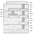
- FIG. 6 is a cross-sectional view schematically showing a stacked structure of the pixel circuit 220.
- FIG. 6 schematically shows a stacked structure from the diffusion layer to the anode of the organic light emitting diode 221 in the pixel circuit 220.
- the pixel circuit 220 includes a plurality of wiring layers 234, 237, and 240 formed on the diffusion layer 231.
- each of the transistors (transistors 222 to 226) is formed by forming an active region functioning as a source region, a drain region, and a channel region, a gate insulating film, a gate electrode, and the like on a semiconductor substrate such as Si. Is formed.
- illustration of elements formed in a diffusion layer such as a transistor is omitted.
- An insulator layer 232 (hereinafter referred to as a first insulator layer 232) is stacked on the diffusion layer 231.
- the first insulator layer 232 is formed by stacking insulators such as silicon oxide (SiO 2 ) with a predetermined thickness (a second insulator layer 235, a third insulator layer 238, and a second insulator layer described later). 4 insulator layer 241 is the same).
- the region and the upper layer are disposed at a position corresponding to a region connected to an upper wiring layer such as each electrode (source electrode, drain electrode, and gate electrode) of each transistor of the diffusion layer 231.
- a contact 233 for electrically connecting a wiring formed in a first wiring layer 234 described later is formed.
- the contact 233 is formed by forming a through hole (contact hole) in the first insulator layer 232 and then embedding a conductor such as tungsten (W) in the contact hole.
- a wiring layer 234 (hereinafter referred to as a first wiring layer 234) is formed on the first insulator layer 232 on which the contact 233 is formed.
- the first wiring layer 234 is formed by laminating a conductor such as aluminum (Al) with a predetermined thickness and then patterning the conductor film into a predetermined shape (a second wiring layer 237, which will be described later). The same applies to the third wiring layer 240).
- a conductor such as aluminum (Al)
- a second wiring layer 237 which will be described later.
- the third wiring layer 240 In the first wiring layer 234, the second wiring layer 237, and / or the third wiring layer 240, each wiring shown in FIG. 5 (various wiring including the H scanning line 228 and the V signal line 229) is formed.
- An insulator layer 235 (hereinafter referred to as a second insulator layer 235) is formed on the first wiring layer 234.
- the second insulator layer 235 is for electrically connecting a corresponding wiring formed in the lower first wiring layer 234 and a corresponding wiring formed in a second wiring layer 237 described later on the upper layer.
- a via 236 (hereinafter referred to as a first via 236) is formed.
- the first via 236 is formed by forming a through hole (via hole) in the second insulator layer 235 and then burying a conductor such as W in the via hole (second via 239 and third described later). The same applies to the via 242).
- a wiring layer 237 (hereinafter referred to as a second wiring layer 237) is formed on the second insulator layer 235 in which the first via 236 is formed.
- An insulator layer 238 (hereinafter referred to as a third insulator layer 238) is formed on the second wiring layer 237.
- the third insulator layer 238 is for electrically connecting a corresponding wiring formed in the lower second wiring layer 237 and a corresponding wiring formed in a third wiring layer 240 described later on the upper layer.
- a via 239 (hereinafter referred to as a second via 239) is formed.
- the wiring layer 240 (hereinafter referred to as the third wiring layer 240) is formed on the third insulator layer 238 in which the second via 239 is formed.
- An insulator layer 241 (hereinafter referred to as a fourth insulator layer 241) is formed on the third wiring layer 240.
- the fourth insulator layer 241 has vias 242 (hereinafter referred to as third vias 242) for electrically connecting corresponding wirings formed in the lower third wiring layer 240 and an anode 243 described later on the upper layer. ) Is formed.
- the pixel circuit 210 is manufactured by forming the organic light emitting diode 211 on the fourth insulator layer 241 in which the third via 242 is formed. Although only the anode 243 of the organic light emitting diode 211 is illustrated in FIG. 6, the organic light emitting diode 211 is formed by sequentially stacking an organic layer functioning as a light emitting layer and a cathode on the anode 243. .
- capacitive elements are formed in the second wiring layer 237 and the third wiring layer 240.
- the lower electrode (capacitor element lower electrode 251) of the capacitor element is formed on the second wiring layer 237.
- An upper electrode (capacitor element upper electrode 252) of the capacitor element is formed on the second wiring layer 237 via an insulator having a thickness corresponding to the capacitance of the capacitor element.
- the capacitive element upper electrode 252 is provided inside the third insulator layer 238. That is, although the description has been omitted above, the third insulator layer 238 is actually laminated in two stages with the capacitor element upper electrode 252 as a boundary.
- an insulator having a thickness corresponding to the capacitance of the capacitor element is laminated, and the capacitor element upper electrode 252 is formed thereon by the same method as that for the wiring layer. Thereafter, a third insulator layer 238 is formed by further laminating an insulator having a predetermined thickness.
- the second via 239 is also provided at a position corresponding to the capacitor element upper electrode 252.
- the capacitor element upper electrode 252 is electrically connected to the electrode 254 formed in the third wiring layer 240 by the second via 239.
- the electrode 254 is for extracting the potential of the capacitive element upper electrode 252 and is an electrode having the same potential as that of the capacitive element upper electrode 252. Therefore, the electrode 254 is also referred to as the capacitive element upper electrode 254 below. I will do it.
- each wiring that is, the H scanning line 228 and the V signal line 229 and the capacitor element (that is, the storage capacitor 227) included in the pixel circuit 210 will be examined.
- each of these wirings is formed in the first wiring layer 234, the second wiring layer 237, and / or the third wiring layer 240.
- the capacitive element lower electrode 251 and the capacitive element upper electrode 254 of the capacitive element are formed in the second wiring layer 237 and the third wiring layer 240, respectively.
- the capacitance element lower electrode 251 and the capacitance element upper electrode 254 of each wiring and the capacitance element can be formed in the same wiring layer.
- deterioration in luminance uniformity due to noise interference between electrodes due to increase in parasitic capacitance between wirings deterioration in luminance uniformity due to noise resistance deterioration due to pressure on the electrode area of the capacitive element
- pixel wiring is dense In other words, there are short circuit defects between wirings, wiring open defects due to skipping of a small area wiring pattern, and the like.
- the first wiring layer 234, the second wiring layer 237, and the third wiring are formed so as to prevent these problems as much as possible while keeping the pixel size small. It is important to devise the layout of the layer 240.
- the present inventors have come up with a suitable layout of the first wiring layer 234, the second wiring layer 237, and the third wiring layer 240 that can avoid the above-described problems.
- the preferred layout will be described in detail with reference to the drawings.
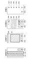
- FIG. 7 is a diagram for explaining an example of the layout of the wiring layer according to the present embodiment. 7 and FIGS. 8 to 10 described later schematically show the layout of the diffusion layer 231, the first wiring layer 234, the second wiring layer 237, and the third wiring layer 240. FIG.
- contacts and vias having “a” at the end of the reference numerals represent contacts and vias that are finally connected to the anode 243 in the upper layer. .
- contacts and vias having “b” at the end of the reference numerals represent contacts and vias that are finally connected to the capacitor lower electrode 251 in the upper layer.
- contacts and vias having “c” at the end of the reference sign represent contacts and vias that are finally connected to the V signal line 229 in the upper layer.
- contacts and vias with “d” at the end of the reference sign represent contacts and vias that are finally connected to the H scanning line 228 in the upper layer.
- the wiring related to the anode 243 (that is, the anode 243) is used for the first wiring layer 234, the second wiring layer 237, and the third wiring layer 240 for explanation.
- the wiring related to the capacitor element lower electrode 251 (that is, the capacitor element lower electrode 251 itself and the capacitor having the same potential as the capacitor element lower electrode 251) are thick solid lines and connected to the V signal line 229.
- the wiring (that is, the V signal line 229 itself and the wiring having the same potential as the V signal line 229) is a one-dot chain line, and the wiring related to the H scanning line 228 (that is, the same as the H scanning line 228 itself and the H scanning line 228).
- the potential wiring is shown by a thin solid line.
- FIG. 7 shows a layout example in the case where the H scanning line 228 and the V signal line 229 are formed in the first wiring layer 234 and the second wiring layer 237.
- the higher number of H scanning lines 228 and V signal lines 229 provided for one pixel circuit 220 is formed in the lower layer.
- the number of H scanning lines 228 provided for one pixel circuit 220 is larger than the number of V signal lines 229. Accordingly, as shown in the figure, if the H scanning line 228 and the V signal line 229 are formed in the first wiring layer 234 and the second wiring layer 237, the H scanning line 228 is formed in the first wiring layer 234. A V signal line 229 is formed in the second wiring layer 237.
- the first wiring layer 234 is connected to the H scanning line 228 and the corresponding electrode of the diffusion layer 231 to the anode 243 formed in the upper layer of the third wiring layer 240.
- Wiring (wiring indicated by a broken line in the drawing; hereinafter also referred to as connecting wiring related to the anode 243), wiring for connecting the corresponding electrode of the diffusion layer 231 to the capacitor element lower electrode 251 formed in the second wiring layer 237 (Wiring shown by a thick solid line in the figure.
- connection wiring relating to the capacitor also referred to as connection wiring relating to the capacitor
- connection wirings related to the V signal line 229 are also referred to as connection wirings related to the V signal line 229.
- connection wirings related to the capacitor element lower electrode 251 and the anode 243 are formed together with the V signal line 229.
- connection wirings related to the capacitor element upper electrode 254 and the anode 243 are formed in the third wiring layer 240. Note that one connection wiring related to the anode 243, one connection wiring related to the capacitor element, and one connection wiring related to the V signal line 229 are formed in each wiring layer.
- FIG. 8 shows a layout example of a wiring layer different from the present embodiment when the H scanning line 228 and the V signal line 229 are formed in the first wiring layer 234 and the second wiring layer 237.
- FIG. 8 is a diagram for comparison with the layout shown in FIG. 7.
- FIG. 6 is a diagram showing an example of a layout when an H scanning line 228 and a V signal line 229 are formed in different wiring layers. As shown in FIG. 8, contrary to the layout according to the present embodiment shown in FIG.
- the first wiring layer 234 includes the V signal line 229, the connection wiring related to the anode 243, the connection wiring related to the capacitor element, and the corresponding electrode of the diffusion layer 231.
- Wiring for connecting to the H scanning line 228 formed in the layer 237 (wiring shown by a thin solid line in the drawing; hereinafter also referred to as connection wiring relating to the H scanning line 228) is formed.
- the number of connection wirings related to the H scanning line 228 is formed according to the number of the H scanning lines 228.
- connection wirings related to the capacitor element lower electrode 251 and the anode 243 are formed together with the H scanning lines 228 in which a larger number exists.
- connection wirings related to the capacitor element upper electrode 254 and the anode 243 are formed in the third wiring layer 240.
- the H scanning line 228 that is a larger number of wirings is the lower first wiring layer 234. Therefore, the wiring pattern of the first wiring layer 234 is relatively dense.
- the H scanning lines 228, which are more wirings are not formed in the first wiring layer 234, but the number of connection wirings related to the H scanning lines 228 corresponds to the number of H scanning lines 228. Only the first wiring layer 234 needs to be formed. Therefore, although the connection wiring related to the H scanning line 228 has a smaller area than the H scanning line 228, as a result, the density of the wiring pattern in the first wiring layer 234 is different from the layout according to the present embodiment. It is not much smaller than that.
- the V signal line 229 which is a smaller number of wires, is formed in the second wiring layer 237, so that the wiring pattern of the second wiring layer 237 is relatively sparse. Become.
- the wiring pattern of the second wiring layer 237 is relatively dense.
- the H scanning lines 228 and the V signal lines 229 are provided on the lower layer of the H scanning lines 228 which are the wirings having a larger number provided for one pixel circuit 220.
- the layout of the first wiring layer 234 and the second wiring layer 237 so as to be formed in the one wiring layer 234, it becomes possible to make the wiring pattern in the second wiring layer 237 in a higher layer more sparse. .
- the sparser wiring pattern in the second wiring layer 237 Due to the sparser wiring pattern in the second wiring layer 237, the above-described deterioration in luminance uniformity due to the increase in the parasitic capacitance between the wirings in the second wiring layer 237, the occurrence of a short circuit failure between the wirings, and the like. It becomes possible to suppress.
- the capacitor element lower electrode 251 since the capacitor element lower electrode 251 is provided in the second wiring layer 237, the wiring pattern of the second wiring layer 237 becomes sparse, so that the flexibility of the layout of the capacitor element lower electrode 251 is increased. In addition, it is possible to secure a sufficient area for realizing the desired capacitance for the capacitor element lower electrode 251.
- FIG. 7 shows one layout example in the case where the H scanning line 228 and the V signal line 229 are formed in the first wiring layer 234 and the second wiring layer 237, respectively, but this embodiment is limited to such an example.
- the layout method according to the present embodiment (that is, a method of forming a higher number of H scanning lines 228 and V signal lines 229 for one pixel circuit 220 in a lower layer) is the H scanning line 228.
- the present invention is applicable even when the V signal line 229 is formed in another wiring layer.
- FIG. 9 is a diagram for explaining another example of the layout of the wiring layer according to the present embodiment.
- FIG. 9 shows a layout example when the H scanning line 228 and the V signal line 229 are formed in the first wiring layer 234, the second wiring layer 237, and the third wiring layer 240.
- the higher number of H scanning lines 228 and V signal lines 229 provided for one pixel circuit 220 is formed in a lower layer.
- the H scanning line 228 is formed in the first wiring layer 234 and the second wiring layer 237
- the V signal line 229 is formed in the third wiring layer 240.
- the first wiring layer 234 includes a part of the H scanning lines 228 (three in the illustrated example), a connection wiring related to the anode 243, and a connection wiring related to the capacitive element. , And a connection wiring relating to the V signal line 229 is formed.
- the remaining H scanning lines 228 are formed, as well as the capacitor element lower electrode 251, the connection wiring for the anode 243, and the connection wiring for the V signal line 229. Is done.
- connection wirings related to the capacitor element upper electrode 254 and the anode 243 are formed together with the V signal line 229.
- the plurality of H scanning lines 228 are formed in the same wiring layer. However, in this embodiment, the plurality of H scanning lines 228 are distributed and formed in different wiring layers. May be.
- FIG. 10 is different from the present embodiment in the case where the H scanning line 228 and the V signal line 229 are formed in the first wiring layer 234, the second wiring layer 237, and the third wiring layer 240.
- An example of a layout of a wiring layer is shown.
- FIG. 10 is a diagram for comparison with the layout shown in FIG. 9, in which the H scanning line 228 and the V signal line 229 are formed in the first wiring layer 234, the second wiring layer 237, and the third wiring layer 240.
- FIG. 4 is a diagram showing a layout example when the H scanning line 228 and the V signal line 229 are formed in a wiring layer different from the present embodiment. As shown in FIG. 10, contrary to the layout according to the present embodiment shown in FIG.
- the larger number of H scanning lines 228 and V signal lines 229 provided for one pixel circuit 220 is It is assumed that the upper layer is formed.
- the V signal line 229 is formed in the first wiring layer 234 and the H scanning line 228 is formed in the third wiring layer 240.
- the first wiring layer 234 is formed with the V signal line 229, the connection wiring related to the anode 243, the connection wiring related to the capacitive element, and the connection wiring related to the H scanning line 228.
- the in the second wiring layer 237 the connection wiring related to the anode 243 and the connection wiring related to the H scanning line 228 are formed together with the capacitor element lower electrode 251.
- the number of connection wirings related to the H scanning line 228 is formed according to the number of the H scanning lines 228.
- connection wirings related to the capacitor element upper electrode 254 and the anode 243 are formed together with the H scanning lines 228 in which a larger number exists.
- the layout according to the present embodiment Comparing the layout according to the present embodiment shown in FIG. 9 with the layout shown in FIG. 10, in the layout according to the present embodiment, most of the H scanning lines 228 which are more wirings are lower first wirings. Since it is formed in the layer 234, the wiring pattern of the first wiring layer 234 is relatively dense. On the other hand, in the layout shown in FIG. 8, the H scanning lines 228, which are more wirings, are not formed in the first wiring layer 234, but the number of connection wirings related to the H scanning lines 228 corresponds to the number of H scanning lines 228. Only the first wiring layer 234 needs to be formed. Therefore, although the connection wiring related to the H scanning line 228 has a smaller area than the H scanning line 228, as a result, the density of the wiring pattern in the first wiring layer 234 is different from the layout according to the present embodiment. It is not much smaller than that.
- the V signal line 229 which is a smaller number of wirings, is formed in the third wiring layer 240. Therefore, the wiring patterns of the second wiring layer 237 and the third wiring layer 240 are used. Is relatively sparse.
- the H scanning line 228, which is the wiring having a larger number of the H scanning lines 228 and the V signal lines 229 provided for one pixel circuit 220, is provided at a lower layer.
- the layout of the first wiring layer 234, the second wiring layer 237, and the third wiring layer 240 so as to be formed in the first wiring layer 234 and the second wiring layer 237, the second wiring layer of the upper layer is formed.
- the wiring patterns in 237 and the third wiring layer 240 can be made sparser. Therefore, it is possible to obtain the same effect as when the layout shown in FIG. 7 described above is applied, that is, it is possible to realize the display device 1 with higher definition and higher reliability.
- a large number of wirings are formed by the lower wiring layer, so that a large number of wirings are formed by the upper wiring layer, and the connection wiring (the above-described H scanning line described above) is isolated from the lower wiring layer.
- the wiring pattern of the lower wiring layer is not less dense.
- the wiring pattern in the lower wiring layer closer to the diffusion layer 231 in which each transistor is formed becomes dense, the light shielding effect on the transistor can be improved. Therefore, the characteristic variation of the transistor due to light exposure can be further suppressed, and the reliability of the display device 1 can be further improved.
- the wiring pattern in the upper wiring layer, particularly the uppermost wiring layer can be made relatively sparse, the anode 243 of the organic light emitting diode 221 formed further above the uppermost wiring layer.
- the flatness of the film can be improved. Thereby, the luminous efficiency of the organic light emitting diode 221 can be improved, and the display quality can be further improved.
- connection wirings related to the anode 243 formed on the third wiring layer 240 which is the uppermost wiring layer that is, The degree of freedom of the arrangement of the third via 242 connecting the connection wiring related to the anode 243 and the upper layer anode 243 is improved. This makes it easier to design the pixel layout.
- FIG. 11 is a diagram illustrating an example of the arrangement of the third vias 242 in the three subpixels when one pixel is formed by the three subpixels.
- FIG. 12 is a diagram illustrating an example of the arrangement of the third vias 242 in the four subpixels when one pixel is formed by the four subpixels.
- FIG. 11 and 12 both are top views of a configuration in which an anode 243 and an organic layer 261 (a layer functioning as a light emitting layer in the organic light emitting diode 221) corresponding to one pixel are stacked on the left side in the drawing.
- the arrangement of the third via 242 for such a configuration is schematically shown.
- the arrangement of the third via 242 for such a configuration is schematically shown.
- the configuration 262 in which the diffusion layer 231 and the wiring layer are stacked is not illustrated in detail inside each layer for the sake of simplicity.
- the structure 262 in which the organic layer 261, the diffusion layer 231 and the wiring layer are stacked has characters (R: Red, G: Green, B: representing the color of the corresponding sub-pixel). Blue, W: White) is added to the end of the code.
- RGB Red, G: Green, B: representing the color of the corresponding sub-pixel
- Blue, W White
- CF color filter
- the arrangement of the third vias 242 is substantially the same in each subpixel. Therefore, there is not much merit by improving the degree of freedom of arrangement of the third via 242.
- the arrangement of the third vias 242 is different in each subpixel. That is, it is necessary to change the arrangement of the connection wiring related to the anode 243 in the third wiring layer 240 for each subpixel.
- the layout as shown in FIG. 10 is performed, if the wiring pattern in the third wiring layer 240 is dense, the degree of freedom of arrangement of the connection wiring related to the anode 243 is low. Therefore, in order to make the arrangement of the connection wiring related to the anode 243 different for each subpixel, there is a possibility that the entire layout of the third wiring layer 240 needs to be different for each subpixel. In this case, the layout of the lower second wiring layer 237 and the first wiring layer 234 may need to be different for each sub-pixel accordingly, so that the amount of work for layout becomes enormous and a heavy burden on the designer. Become.
- the wiring pattern of the upper wiring layer can be made relatively sparse, so that the degree of freedom of the arrangement of the connection wiring related to the anode 243 in the third wiring layer 240 is increased. high. Therefore, the layout of the third wiring layer 240 can be configured so that only the arrangement of the connection wirings related to the anode 243 is different for each subpixel, and the other wirings are the same for each subpixel. In this case, regarding the layout of the lower second wiring layer 237 and the first wiring layer 234, only the arrangement of the connection wiring related to the anode 243 needs to be different for each sub-pixel, so that the difficulty in designing the layout is lowered.
- the third via 242 (that is, the uppermost wiring layer and the uppermost wiring layer) is formed for each subpixel as in the case where one pixel is formed by four subpixels.
- the arrangement of vias connecting to the anode 243 is different, there is also an effect that the difficulty of layout design of the pixel can be reduced.
- the wiring layer layout according to the present embodiment has been described above. In the above, only the two layout examples shown in FIGS. 7 and 9 are taken up. However, when the number of wiring layers is different from the three layers exemplified above (for example, when there are more than four layers), When the arrangement positions of the H scanning lines 228 and the V signal lines 229 in the wiring layer are different, when the numbers of the H scanning lines 228 and the V signal lines 229 are different (for example, when there are a plurality of both), one pixel circuit 210, Even when the magnitude relationship between the numbers of the H scanning lines 228 and the V signal lines 229 provided for 220 is opposite, the wiring layer layout method according to the present embodiment can be applied.
- the wiring layer layout method according to the present embodiment can be applied to various display devices as long as the display device is driven by an active matrix method. Regardless of the number of wiring layers and the like, the number of connection wirings related to the H scanning line 228 or V signal line 229 in the lower wiring layer is applied by applying the wiring layer layout method according to the present embodiment. As a result, the wiring pattern of the upper wiring layer can be made relatively sparse. Further, by providing a capacitor element electrode (capacitor element lower electrode 251 and / or capacitor element upper electrode 254) in a wiring layer having a relatively sparse wiring pattern, a sufficient area of the capacitor element electrode is ensured. be able to. Accordingly, as in the above-described embodiment, various effects such as improved reliability can be obtained.
- FIG. 13 is a cross-sectional view illustrating a specific configuration example of the display device 1 according to the present embodiment.
- FIG. 13 shows a partial cross-sectional view of the display device 1.
- the display device 1 is provided on a first substrate 11 with a plurality of organic light emitting diodes 211 that are light emitting elements that emit white light, and an upper layer of the organic light emitting diodes 211.
- a second substrate 34 formed of a material transparent to the light from the organic light emitting diode 211 is disposed on the CF layer 33.
- the first substrate 11 is provided with a thin film transistor (TFT) 15 for driving the organic light emitting diode 211 corresponding to each of the organic light emitting diodes 211.
- TFT thin film transistor
- the TFT 15 corresponds to each transistor (the driving transistor 212, the sampling transistor 213, the light emission control transistor 214, and the switching transistor 217) that constitutes the pixel circuit 210 described above.
- An arbitrary organic light emitting diode 211 is selectively driven by the TFT 15, and the light from the driven organic light emitting diode 211 passes through the corresponding CF so that the color is appropriately converted, and from above through the second substrate 34.
- a desired image, a character, etc. are displayed by being emitted.
- the stacking direction of the layers in the display device 1 is also referred to as the vertical direction.
- the direction in which the first substrate 11 is disposed is defined as a downward direction
- the direction in which the second substrate 34 is disposed is defined as an upward direction.
- a surface perpendicular to the vertical direction is also referred to as a horizontal plane.
- the display device 1 shown in FIG. 13 is a top emission type display device that can be displayed in color and is driven by an active matrix method.
- this embodiment is not limited to such an example, and the display device 1 according to this embodiment may be a bottom emission type display device that emits light through the first substrate 11.
- the first substrate 11 is composed of a Si substrate.
- the second substrate 34 is made of quartz glass.
- this embodiment is not limited to this example, and various known materials may be used for the first substrate 11 and the second substrate 34.
- the first substrate 11 and the second substrate 34 are a high strain point glass substrate, a soda glass (mixture of Na 2 O, CaO and SiO 2 ) substrate, a borosilicate glass (Na 2 O, B 2 O 3 and SiO 2).
- substrate 34 may be the same, and may differ. However, since the display device 1 is a top emission type as described above, the second substrate 34 is preferably formed of a material having a high transmittance that can suitably transmit the light from the organic light emitting diode 211.
- the organic light emitting diode 211 includes a first electrode 21, an organic layer 23 provided on the first electrode 21, and a second electrode 22 formed on the organic layer 23. More specifically, a second member 52 provided with an opening 25 so as to expose at least a part of the first electrode 21 is laminated on the first electrode 21, and the organic layer 23 is It is provided on the first electrode 21 exposed at the bottom of the opening 25. That is, the organic light emitting diode 211 has a configuration in which the first electrode 21, the organic layer 23, and the second electrode 22 are stacked in this order in the opening 25 of the second member 52. This stacked structure functions as the light emitting portion 24 of each pixel. That is, the portion of the organic light emitting diode 211 that contacts the opening 25 of the second member 52 is the light emitting surface.
- the second member 52 functions as a pixel definition film that is provided between the pixels and defines the area of the pixels.
- the organic layer 23 includes a light emitting layer made of an organic light emitting material and is configured to emit white light.
- the specific configuration of the organic layer 23 is not limited, and may be various known configurations.
- the organic layer 23 has a stacked structure of a hole transport layer, a light emitting layer, and an electron transport layer, a stacked structure of a hole transport layer and a light emitting layer that also serves as an electron transport layer, or a hole injection layer and a hole transport. It can be composed of a laminated structure of a layer, a light emitting layer, an electron transport layer, and an electron injection layer.
- the organic layer 23 may have a two-stage tandem structure in which a first tandem unit, a connection layer, and a second tandem unit are laminated. Good.
- the organic layer 23 may have a three or more tandem structure in which three or more tandem units are stacked.
- the organic layer 23 that emits white as a whole can be obtained by changing the luminescent color of the light emitting layer between red, green, and blue in each tandem unit.
- the organic layer 23 is formed by vacuum-depositing an organic material.
- the organic layer 23 may be formed by various known methods.
- the organic layer 23 may be formed by a physical vapor deposition method (PVD method) such as a vacuum deposition method, a printing method such as a screen printing method or an ink jet printing method, a laser absorption layer formed on a transfer substrate, and the like.
- PVD method physical vapor deposition method
- a laser transfer method in which the organic layer on the laser absorption layer is separated by irradiating a laser on the stacked structure of the organic layer and the organic layer is transferred, or various coating methods can be used.
- the first electrode 21 functions as an anode. That is, the first electrode 21 corresponds to the anode 243 shown in FIG. Since the display device 1 is a top emission type as described above, the first electrode 21 is formed of a material that can reflect light from the organic layer 23. In the illustrated configuration example, the first electrode 21 is formed of an alloy of aluminum and neodymium (Al—Nd alloy). The film thickness of the first electrode 21 is, for example, about 0.1 ⁇ m to 1 ⁇ m. However, the present embodiment is not limited to such an example, and the first electrode 21 is formed of various known materials used as a material for a light reflection side electrode that functions as an anode in a general organic EL display device. can do. Further, the film thickness of the first electrode 21 is not limited to the above example, and the first electrode 21 can be appropriately formed within a film thickness range generally employed in an organic EL display device.
- the first electrode 21 includes platinum (Pt), gold (Au), silver (Ag), chromium (Cr), tungsten (W), nickel (Ni), copper (Cu), iron (Fe), cobalt ( Co) or a metal having a high work function such as tantalum (Ta), or an alloy (for example, 0.3% by mass to 1% by mass of palladium (Pd) and 0.3% by mass to 1% by mass of silver as a main component)
- a metal having a high work function such as tantalum (Ta), or an alloy (for example, 0.3% by mass to 1% by mass of palladium (Pd) and 0.3% by mass to 1% by mass of silver as a main component)
- an Ag—Pd—Cu alloy containing 1% copper or an Al—Nd alloy for example, an Ag—Pd—Cu alloy containing 1% copper or an Al—Nd alloy.
- a conductive material having a small work function value and high light reflectance such as aluminum or an alloy containing aluminum can be used
- the first electrode 21 has a hole injection property such as an oxide of indium and tin (ITO) or an oxide of indium and zinc (IZO) on a highly reflective film such as a dielectric multilayer film or aluminum. It is also possible to have a structure in which transparent conductive materials excellent in thickness are laminated.
- ITO indium and tin
- IZO oxide of indium and zinc
- the second electrode 22 functions as a cathode.
- the second electrode 22 is formed of a material that can transmit light from the organic layer 23.
- the second electrode 22 is formed of an alloy of magnesium and silver (Mg—Ag alloy).
- the film thickness of the second electrode 22 is, for example, about 10 nm.
- the present embodiment is not limited to this example, and the second electrode 22 is formed of various known materials that are used as a material of an electrode on the light transmission side that functions as a cathode in a general organic EL display device. can do.
- the film thickness of the second electrode 22 is not limited to the above example, and the second electrode 22 can be appropriately formed within a film thickness range generally employed in an organic EL display device.
- the second electrode 22 is made of aluminum, silver, magnesium, calcium (Ca), sodium (Na), strontium (Sr), an alloy of alkali metal and silver, or an alloy of alkaline earth metal and silver (for example, magnesium). And an alloy of Mg and Ag (Mg—Ag alloy), an alloy of magnesium and calcium (Mg—Ca alloy), an alloy of aluminum and lithium (Al—Li alloy), and the like.
- the thickness of the second electrode 22 is, for example, about 4 nm to 50 nm.
- the second electrode 22 may have a structure in which the material layer described above and a transparent electrode made of, for example, ITO or IZO (for example, a thickness of about 30 nm to 1 ⁇ m) are stacked from the organic layer 23 side.
- a transparent electrode made of, for example, ITO or IZO (for example, a thickness of about 30 nm to 1 ⁇ m)
- the thickness of the material layer described above can be reduced to, for example, about 1 nm to 4 nm.
- the 2nd electrode 22 may be comprised only with a transparent electrode.
- a bus electrode (auxiliary electrode) made of a low resistance material such as aluminum, aluminum alloy, silver, silver alloy, copper, copper alloy, gold, or gold alloy is provided for the second electrode 22, and the second electrode 22 as a whole. The resistance may be reduced.
- the first electrode 21 and the second electrode 22 are formed by depositing a material by a predetermined thickness by a vacuum evaporation method and then patterning the film by an etching method.
- this embodiment is not limited to this example, and the first electrode 21 and the second electrode 22 may be formed by various known methods.
- the method for forming the first electrode 21 and the second electrode 22 include an electron beam vapor deposition method, a hot filament vapor deposition method, a vapor deposition method including a vacuum vapor deposition method, a sputtering method, a chemical vapor deposition method (CVD method), and an organic method.
- MOCVD Metal chemical vapor deposition
- various printing methods for example, screen printing, ink jet printing, or metal mask printing
- plating (electroplating) Method for example, electroless plating method, etc.
- lift-off method for example, laser ablation method, sol-gel method and the like.
- the second member 52 is formed by depositing SiO 2 to a predetermined thickness by a CVD method and then patterning the SiO 2 film using a photolithography technique and an etching technique.
- the material of the second member 52 is not limited to this example, and various materials having insulating properties can be used as the material of the second member 52.
- examples of the material constituting the second member 52 include SiO 2 , MgF, LiF, polyimide resin, acrylic resin, fluororesin, silicone resin, fluoropolymer, and silicone polymer.
- the second member 52 is formed of a material having a refractive index lower than that of the material of the first member 51.
- the first electrode 21 constituting the organic light emitting diode 211 is provided on the interlayer insulating layer 16 made of SiON.
- the interlayer insulating layer 16 covers the light emitting element driving unit formed on the first substrate 11.
- the light emitting element driving unit is composed of a plurality of TFTs 15. That is, the light emitting element driving unit corresponds to the driving circuit of the pixel circuit 210.
- the TFT 15 includes a gate electrode 12 formed on the first substrate 11, a gate insulating film 13 formed on the first substrate 11 and the gate electrode 12, and a semiconductor layer 14 formed on the gate insulating film 13.
- the TFT 15 is a bottom gate type, but the present embodiment is not limited to this example, and the TFT 15 may be a top gate type.
- An interlayer insulating layer 16 (a lower interlayer insulating layer 16A and an upper interlayer insulating layer 16B) having two layers is laminated on the upper layer of the semiconductor layer 14 by a CVD method.
- the source / drain region 14B is exposed to a portion corresponding to the source / drain region 14B of the lower interlayer insulating layer 16A using, for example, a photolithography technique and an etching technique.
- a contact hole 17 is provided in the substrate, and a wiring 18 made of aluminum is formed so as to fill the contact hole 17.
- the wiring 18 is formed by combining, for example, a vacuum deposition method and an etching method.
- the upper interlayer insulating layer 16B is laminated.
- a contact hole 19 is provided in a portion of the upper interlayer insulating layer 16B where the wiring 18 is provided so as to expose the wiring 18 by using, for example, a photolithography technique and an etching technique.
- the first electrode 21 of the organic light emitting diode 211 is formed, the first electrode 21 is formed so as to be in contact with the wiring 18 through the contact hole 19.
- the organic light emitting diode 211 has a first electrode 21 corresponding to the source / drain region 14B of the TFT 15 via the wiring 18 (in the pixel circuit example shown in FIG. ) And electrically connected.
- the interlayer insulating layer 16 is made of SiON, but the present embodiment is not limited to this example.
- the interlayer insulating layer 16 may be formed of various known materials that can be used as an interlayer insulating layer in a general organic EL display device.
- a SiO 2 material for example, SiO 2 , BPSG, PSG, BSG, AsSG, PbSG, SiON, SOG (spin on glass), low melting glass, glass paste, etc.
- SiN materials and insulating resins for example, polyimide resins, novolac resins, acrylic resins, polybenzoxazoles, etc.
- insulating resins for example, polyimide resins, novolac resins, acrylic resins, polybenzoxazoles, etc.
- the method for forming the interlayer insulating layer 16 is not limited to the above example, and the interlayer insulating layer 16 can be formed by a known method such as a CVD method, a coating method, a sputtering method, or various printing methods. .
- the wiring 18 is formed by forming and patterning aluminum by vacuum deposition and etching, but this embodiment is not limited to this example.
- the wiring 18 may be formed by forming and patterning various materials used as wiring in a general organic EL display device by various methods.
- FIG. 13 only one wiring layer is shown for simplicity. Actually, as described with reference to FIG. 6, a plurality of wiring layers may be formed on the diffusion layer on which the TFT 15 is formed, and the organic light emitting diode 211 may be further formed thereon.
- the opening 25 provided in the second member 52 of the organic light emitting diode 211 is formed such that its sidewall has a tapered shape that is inclined so that the opening area increases as it goes downward.
- the first member 51 is embedded in the opening 25. That is, the first member 51 is a layer that is provided immediately above the light emitting surface of the organic light emitting diode 211 and propagates light emitted from the light emitting element upward.
- the first member 51 has a substantially trapezoidal cross-sectional shape in the stacking direction (that is, the cross-sectional shape shown in the drawing), and a bottom surface on the upper side. Has a truncated pyramid shape.
- the first member 51 is formed by depositing Si 1-x N x by vacuum deposition so as to fill the opening 25, and then the surface of the Si 1-x N x film is formed by chemical mechanical polishing (CMP method) or the like. It is formed by flattening.
- the material of the first member 51 is not limited to this example, and as the material of the first member 51, various materials having insulating properties can be used.
- the material constituting the first member 51 includes Si 1-x N x , ITO, IZO, TiO 2 , Nb 2 O 5 , bromine-containing polymer, sulfur-containing polymer, titanium-containing polymer, or zirconium-containing polymer. Can be mentioned.
- the method for forming the first member 51 is not limited to this example, and various known methods may be used as the method for forming the first member 51.
- the refractive index n 1 of the first member 51 so that the refractive index n 2 of the second member 52 satisfies the relationship of n 1> n 2
- the first member 51 and second member 52 Materials are selected.
- the first member 51 is provided immediately above the light emitting surface of the organic light emitting diode 211 as described above. Since the first member 51 has a truncated pyramid shape with the bottom surface facing upward, the light emitted from the light emitting surface of the organic light emitting diode 211 is the interface between the first member 51 and the second member 52, that is, The light is reflected upward by the reflector 53, which is the light emission direction.
- the reflector 53 by providing the reflector 53, the extraction efficiency of the emitted light from the organic light emitting diode 211 can be improved, and the luminance of the display device 1 as a whole can be improved.
- the refractive indexes of the first member 51 and the second member 52 are n 1 ⁇ n. It is preferable to satisfy the relationship of 2 ⁇ 0.20. More preferably, it is desirable that the refractive indexes of the first member 51 and the second member 52 satisfy a relationship of n 1 ⁇ n 2 ⁇ 0.30.
- the shape of the first member 51 is such that 0.5 ⁇ R 1 / R 2 ⁇ 0.8 and 0.5 ⁇ H / It is preferable to satisfy the relationship of R 1 ⁇ 0.8.
- R 1 is the diameter of the light incident surface of the first member 51 (that is, the portion facing downward in the stacking direction and facing the light emitting surface of the organic light emitting diode 211), and R 2 is the first member.
- H is the distance (height in the stacking direction) between the bottom surface and the top surface when the first member 51 is regarded as a truncated cone. is there.
- a protective film 31 and a planarizing film 32 are stacked in this order on the planarized first member 51.
- the protective film 31 is formed, for example, by stacking Si 1-y N y by a predetermined film thickness (about 3.0 ⁇ m) by vacuum deposition.
- the planarizing film 32 is formed, for example, by laminating SiO 2 by a predetermined film thickness (about 2.0 ⁇ m) by a CVD method and planarizing the surface by a CMP method or the like.
- the material and film thickness of the protective film 31 and the planarizing film 32 are not limited to this example, and the protective film 31 and the planarizing film 32 are used as a protective film and a planarizing film for a general organic EL display device. Depending on the various known materials, it may be appropriately formed so as to have a film thickness generally employed in organic EL display devices.
- the protective film 31 has a refractive index n 3 that is equal to or smaller than the refractive index n 1 of the first member 51 or the refractive index n 1 of the first member 51. 31 materials are selected. Further, preferably, the refractive index n 3 of the protective film 31, the absolute value of the difference between the refractive index n 4 of the planarization film 32 is 0.30 or less, more preferably to be 0.20 or less, the protective film 31 and the material of the planarizing film 32 are selected.
- the light emitted from the organic light emitting diode 211 is transmitted to the interface between the first member 51 and the protective film 31, and the protective film 31 and the planarizing film 32. Can be suppressed from being reflected or scattered at the interface with the light, and the light extraction efficiency can be further improved.
- the display device 1 is a so-called on-chip color filter (OCCF) type display device in which the CF layer 33 is formed on the first substrate 11 on which the organic light emitting diode 211 is formed.
- the display device 1 is manufactured by attaching the second substrate 34 to the upper layer of the CF layer 33 via a sealing resin film 35 such as an epoxy resin.
- a sealing resin film 35 such as an epoxy resin.
- the material of the sealing resin film 35 is not limited to this example, and the material of the sealing resin film 35 is highly transmissive to the light emitted from the organic light emitting diode 211, and the CF layer 33 and the upper layer located in the lower layer.
- the display device 1 includes the first substrate 11 such that the CF layer 33 is formed on the second substrate 34 and the CF layer 33 faces the organic light emitting diode 211. It may be a so-called counter-CF display device manufactured by bonding the second substrate 34 and the second substrate 34 together.
- the CF layer 33 is formed so that each color CF having a predetermined area is provided for each of the organic light emitting diodes 211.
- the CF layer 33 can be formed, for example, by exposing and developing a resist material in a predetermined shape using a photolithography technique.
- the film thickness of the CF layer 33 is, for example, about 2 ⁇ m.
- the material, the forming method, and the film thickness of the CF layer 33 are not limited to such examples, and the CF layer 33 may be any of various known materials used as a CF layer in a general organic EL display device, and various types of materials. It may be appropriately formed by a known method so as to have a film thickness generally employed in an organic EL display device.
- the CF layer 33 is configured such that red CF33R, green CF33G, and blue CF33B each having a predetermined area are continuously distributed in a horizontal plane.
- red CF33R, green CF33G, and blue CF33B each having a predetermined area are continuously distributed in a horizontal plane.
- CF33a when it is not necessary to distinguish between CF33R, CF33G, and CF33B, one or more of them are simply referred to as CF33a.
- One sub-pixel is formed by a combination of one organic light emitting diode 211 and one CF 33a.
- the specific configuration example of the display device 1 has been described above.
- the configuration of the display device 1 described above particularly the configuration of the reflector 53, reference can be made to, for example, Japanese Patent Application Laid-Open No. 2013-191533, which is a prior application by the present applicant.
- the configuration of the display device 1 according to the present embodiment is not limited to such an example.
- the display device 1 according to the present embodiment only needs to reflect the points described in (4. Layout of wiring layers), and other points are used in a general display device.
- Various known configurations can be applied.
- FIG. 14 is a diagram illustrating an appearance of a smartphone, which is an example of an electronic device to which the display device 1 according to this embodiment can be applied.
- the smartphone 501 includes an operation unit 503 that includes buttons and receives an operation input by a user, and a display unit 505 that displays various types of information.
- the display device 1 can be applied to the display unit 505.
- FIGS. 15 and 16 are views showing the appearance of a digital camera, which is another example of an electronic apparatus to which the display device 1 according to this embodiment can be applied.
- FIG. 15 shows an appearance of the digital camera 511 viewed from the front (subject side)
- FIG. 16 shows an appearance of the digital camera 511 viewed from the rear.
- the digital camera 511 displays a main body (camera body) 513, an interchangeable lens unit 515, a grip 517 held by a user at the time of shooting, and various types of information.
- a monitor 519 and an electronic view finder (EVF) 521 that displays a through image observed by the user at the time of shooting.
- the display device 1 can be applied to the monitor 519 and the EVF 521.
- FIG. 17 is a diagram illustrating an appearance of a head mounted display (HMD), which is another example of an electronic apparatus to which the display device 1 according to the present embodiment can be applied.
- the HMD 531 includes a glasses-shaped display unit 533 that displays various types of information, and an ear hooking unit 535 that is hooked on the user's ear when worn.
- the display device 1 can be applied to the display unit 533.
- the electronic apparatus to which the display device 1 can be applied is not limited to those exemplified above, and the display device 1 may be, for example, a television device, an electronic book, a smartphone, a portable information terminal (PDA: Personal Digital Assistant), a notebook, or the like. Applicable to display devices mounted on electronic devices in all fields that display based on externally input image signals or internally generated image signals such as type PCs (Personal Computers), video cameras, or game machines Is possible.
- type PCs Personal Computers
- video cameras or game machines
- each transistor (the driving transistor 212, the sampling transistor 213, the light emission control transistor 214, and the switching transistor 217) included in the driving circuit of the pixel circuit 210 is a P-channel type.
- Such a technique is not limited to such an example.
- these transistors may be N-channel type.
- a pixel unit configured by arranging a plurality of pixel circuits each including a light emitting element and a driving circuit for driving the light emitting element in a matrix; and A wiring connected to each of the pixel circuits, the scanning line provided extending in a first direction corresponding to each row of the plurality of pixel circuits; A wiring connected to each of the pixel circuits, the signal line extending in a second direction orthogonal to the first direction corresponding to each column of the plurality of pixel circuits;
- the larger number provided for one pixel circuit is located in a lower wiring layer
- the electrode of the capacitive element included in the drive circuit is located in a wiring layer provided with either the scanning line or the signal line.
- the drive circuit has a plurality of transistors, A plurality of wiring layers in which the scanning lines, the signal lines, and the capacitor elements are formed are stacked on a diffusion layer in which a plurality of the transistors are formed.
- the light emitting element is an organic light emitting diode;
- the organic light emitting diode is located on the uppermost wiring layer;
- One subpixel is constituted by one pixel circuit, One pixel is constituted by the four sub-pixels.
- the number of scanning lines is greater than the number of signal lines, The display device according to any one of (1) to (4).
- the scanning line is a wiring extending in a horizontal direction
- the signal line is a wiring extending in the vertical direction.
- the display device according to any one of (1) to (5).
- All of the plurality of scanning lines are located in the same wiring layer, or all of the plurality of signal lines are located in the same wiring layer, The display device according to any one of (1) to (6).
- a plurality of the scanning lines are arranged in a plurality of different wiring layers, or a plurality of the signal lines are arranged in a plurality of different wiring layers.
- a display device for performing display based on a video signal With The display device A pixel unit configured by arranging a plurality of pixel circuits each including a light emitting element and a driving circuit for driving the light emitting element in a matrix; and A wiring connected to each of the pixel circuits, the scanning line provided extending in a first direction corresponding to each row of the plurality of pixel circuits; A wiring connected to each of the pixel circuits, the signal line extending in a second direction orthogonal to the first direction corresponding to each column of the plurality of pixel circuits; Have Of the scanning lines and the signal lines, the larger number provided for one pixel circuit is located in a lower wiring layer, The electrode of the capacitive element included in the drive circuit is located in a wiring layer provided with either the scanning line or the signal line. Electronics.
Landscapes
- Engineering & Computer Science (AREA)
- Microelectronics & Electronic Packaging (AREA)
- Physics & Mathematics (AREA)
- Geometry (AREA)
- Chemical & Material Sciences (AREA)
- Inorganic Chemistry (AREA)
- Theoretical Computer Science (AREA)
- General Physics & Mathematics (AREA)
- Computer Hardware Design (AREA)
- Optics & Photonics (AREA)
- Sustainable Development (AREA)
- Life Sciences & Earth Sciences (AREA)
- Electroluminescent Light Sources (AREA)
- Control Of El Displays (AREA)
- Control Of Indicators Other Than Cathode Ray Tubes (AREA)
- Devices For Indicating Variable Information By Combining Individual Elements (AREA)
Abstract
Le problème décrit par la présente invention est de rendre possible d'autres améliorations de fiabilité. La solution selon l'invention porte sur un dispositif d'affichage comprenant : une unité de pixels constituée par l'agencement d'une pluralité de circuits de pixels constitués d'éléments électroluminescents et de circuits de pilotage afin de piloter les éléments électroluminescents sous une forme de matrice ; des lignes de balayage connectées par câblage à chacun des circuits de pixels et disposées de façon à s'étendre dans une première direction correspondant à chaque rangée de la pluralité de circuits de pixels ; et des lignes de signal connectées par câblage à chacun des circuits de pixel et disposées de façon à s'étendre dans une seconde direction perpendiculaire à la première direction correspondant à chaque colonne de la pluralité de circuits de pixels. N'importe lesquelles des lignes de balayage ou des lignes de signal possédant davantage de lignes pour un seul circuit de pixels sont positionnées dans une couche de câblage inférieure et des électrodes pour des éléments de capacité compris dans les circuits de pilotage sont positionnées dans n'importe quelle couche de câblage pour les lignes de balayage ou les lignes de signal.
Priority Applications (11)
| Application Number | Priority Date | Filing Date | Title |
|---|---|---|---|
| CN201780056762.5A CN109716422B (zh) | 2016-09-21 | 2017-07-27 | 显示装置和电子设备 |
| DE112017004729.3T DE112017004729T5 (de) | 2016-09-21 | 2017-07-27 | Anzeigevorrichtung und elektronische vorrichtung |
| CN202111081274.4A CN113809137B (zh) | 2016-09-21 | 2017-07-27 | 显示装置和电子设备 |
| US16/323,616 US10839752B2 (en) | 2016-09-21 | 2017-07-27 | Display device and electronic apparatus |
| JP2018540664A JPWO2018055902A1 (ja) | 2016-09-21 | 2017-07-27 | 表示装置及び電子機器 |
| US17/067,163 US11430389B2 (en) | 2016-09-21 | 2020-10-09 | Display device and electronic apparatus |
| JP2021188563A JP7168749B2 (ja) | 2016-09-21 | 2021-11-19 | 表示装置 |
| US17/871,204 US11705072B2 (en) | 2016-09-21 | 2022-07-22 | Display device and electronic apparatus |
| US18/323,062 US11978405B2 (en) | 2016-09-21 | 2023-05-24 | Display device and electronic apparatus |
| US18/633,194 US12266314B2 (en) | 2016-09-21 | 2024-04-11 | Display device and electronic apparatus |
| US19/077,744 US20250292738A1 (en) | 2016-09-21 | 2025-03-12 | Display device and electronic apparatus |
Applications Claiming Priority (2)
| Application Number | Priority Date | Filing Date | Title |
|---|---|---|---|
| JP2016-184280 | 2016-09-21 | ||
| JP2016184280 | 2016-09-21 |
Related Child Applications (2)
| Application Number | Title | Priority Date | Filing Date |
|---|---|---|---|
| US16/323,616 A-371-Of-International US10839752B2 (en) | 2016-09-21 | 2017-07-27 | Display device and electronic apparatus |
| US17/067,163 Continuation US11430389B2 (en) | 2016-09-21 | 2020-10-09 | Display device and electronic apparatus |
Publications (1)
| Publication Number | Publication Date |
|---|---|
| WO2018055902A1 true WO2018055902A1 (fr) | 2018-03-29 |
Family
ID=61690340
Family Applications (1)
| Application Number | Title | Priority Date | Filing Date |
|---|---|---|---|
| PCT/JP2017/027160 Ceased WO2018055902A1 (fr) | 2016-09-21 | 2017-07-27 | Dispositif d'affichage et dispositif électronique |
Country Status (5)
| Country | Link |
|---|---|
| US (6) | US10839752B2 (fr) |
| JP (2) | JPWO2018055902A1 (fr) |
| CN (3) | CN109716422B (fr) |
| DE (1) | DE112017004729T5 (fr) |
| WO (1) | WO2018055902A1 (fr) |
Cited By (1)
| Publication number | Priority date | Publication date | Assignee | Title |
|---|---|---|---|---|
| JP2023534083A (ja) * | 2020-05-15 | 2023-08-08 | 京東方科技集團股▲ふん▼有限公司 | 表示パネル及びその製作方法、表示装置 |
Families Citing this family (10)
| Publication number | Priority date | Publication date | Assignee | Title |
|---|---|---|---|---|
| JP6201465B2 (ja) * | 2013-07-08 | 2017-09-27 | ソニー株式会社 | 表示装置、表示装置の駆動方法、及び、電子機器 |
| US11551611B2 (en) * | 2018-12-18 | 2023-01-10 | Samsung Display Co., Ltd. | Pixel circuit and organic light emitting display device including i he same |
| KR102845810B1 (ko) * | 2019-07-17 | 2025-08-13 | 삼성디스플레이 주식회사 | 표시 장치 |
| US11800761B2 (en) | 2019-08-01 | 2023-10-24 | V-Finity, Inc. | LED display with pixel circuitry disposed on a substrate backside |
| US11476320B2 (en) * | 2019-08-01 | 2022-10-18 | V-Finity, Inc. | Flat panel LED display |
| EP4131246A4 (fr) * | 2020-03-27 | 2023-04-26 | BOE Technology Group Co., Ltd. | Panneau d'affichage et appareil d'affichage |
| CN112614829B (zh) * | 2020-12-17 | 2024-10-29 | 深圳Tcl数字技术有限公司 | 封装载板以及显示装置 |
| US12057067B2 (en) * | 2022-03-31 | 2024-08-06 | Meta Platforms Technologies, Llc | Self-compensation of driving transistor threshold voltage using body effect |
| WO2024130510A1 (fr) * | 2022-12-19 | 2024-06-27 | 京东方科技集团股份有限公司 | Substrat d'affichage et appareil d'affichage |
| CN116312345A (zh) * | 2023-01-19 | 2023-06-23 | 京东方科技集团股份有限公司 | 显示模组、驱动方法、显示面板和显示装置 |
Citations (3)
| Publication number | Priority date | Publication date | Assignee | Title |
|---|---|---|---|---|
| JP2015111275A (ja) * | 2005-07-04 | 2015-06-18 | 株式会社半導体エネルギー研究所 | 表示装置 |
| JP2016053641A (ja) * | 2014-09-03 | 2016-04-14 | セイコーエプソン株式会社 | 有機エレクトロルミネッセンス装置および電子機器 |
| JP2016154229A (ja) * | 2015-02-12 | 2016-08-25 | 株式会社半導体エネルギー研究所 | 半導体装置、または該半導体装置を有する表示装置 |
Family Cites Families (46)
| Publication number | Priority date | Publication date | Assignee | Title |
|---|---|---|---|---|
| JP3756326B2 (ja) * | 1998-08-24 | 2006-03-15 | シャープ株式会社 | 液晶表示装置 |
| JP2002353245A (ja) * | 2001-03-23 | 2002-12-06 | Seiko Epson Corp | 電気光学基板装置及びその製造方法、電気光学装置、電子機器、並びに基板装置の製造方法 |
| JP3788916B2 (ja) * | 2001-03-30 | 2006-06-21 | 株式会社日立製作所 | 発光型表示装置 |
| CN1252525C (zh) * | 2002-07-24 | 2006-04-19 | Nec液晶技术株式会社 | 有源矩阵型液晶显示器件及其制造方法 |
| JP4042548B2 (ja) * | 2002-11-29 | 2008-02-06 | セイコーエプソン株式会社 | 電気光学装置及び電子機器 |
| JP4089544B2 (ja) * | 2002-12-11 | 2008-05-28 | ソニー株式会社 | 表示装置及び表示装置の製造方法 |
| KR100570763B1 (ko) * | 2004-04-29 | 2006-04-12 | 삼성에스디아이 주식회사 | 발광 표시 패널 및 발광 표시 장치 |
| JP2006071861A (ja) * | 2004-09-01 | 2006-03-16 | Seiko Epson Corp | 電気光学装置及び電子機器 |
| US20060139551A1 (en) * | 2004-12-27 | 2006-06-29 | Yohei Kimura | Display device |
| JP4636006B2 (ja) * | 2005-11-14 | 2011-02-23 | ソニー株式会社 | 画素回路及び画素回路の駆動方法、表示装置及び表示装置の駆動方法、並びに、電子機器 |
| JP5092306B2 (ja) * | 2006-08-02 | 2012-12-05 | ソニー株式会社 | 表示装置および画素回路のレイアウト方法 |
| JP5261900B2 (ja) * | 2006-08-23 | 2013-08-14 | ソニー株式会社 | 画素回路 |
| JP5151172B2 (ja) * | 2007-02-14 | 2013-02-27 | ソニー株式会社 | 画素回路および表示装置 |
| KR20080082400A (ko) * | 2007-03-08 | 2008-09-11 | 엘지전자 주식회사 | 전계발광소자 및 이의 제조방법 |
| JP2008233399A (ja) * | 2007-03-19 | 2008-10-02 | Sony Corp | 画素回路および表示装置、並びに表示装置の製造方法 |
| JP5056265B2 (ja) * | 2007-08-15 | 2012-10-24 | ソニー株式会社 | 表示装置および電子機器 |
| JP4582195B2 (ja) * | 2008-05-29 | 2010-11-17 | ソニー株式会社 | 表示装置 |
| JP2010113230A (ja) * | 2008-11-07 | 2010-05-20 | Sony Corp | 画素回路及び表示装置と電子機器 |
| KR101740943B1 (ko) * | 2009-09-24 | 2017-06-15 | 가부시키가이샤 한도오따이 에네루기 켄큐쇼 | 표시 장치 |
| JP6082907B2 (ja) | 2012-02-17 | 2017-02-22 | 株式会社Joled | 表示装置及び表示装置の製造方法 |
| TWI460704B (zh) * | 2012-03-21 | 2014-11-11 | Innocom Tech Shenzhen Co Ltd | 顯示器及其驅動方法 |
| JP2014013301A (ja) * | 2012-07-04 | 2014-01-23 | Seiko Epson Corp | 電気光学装置、及び電子機器 |
| JP2014048485A (ja) * | 2012-08-31 | 2014-03-17 | Sony Corp | 表示装置及び電子機器 |
| TW201426709A (zh) | 2012-12-26 | 2014-07-01 | Sony Corp | 顯示裝置、顯示裝置之驅動方法及電子機器 |
| JP2014186200A (ja) * | 2013-03-25 | 2014-10-02 | Seiko Epson Corp | 電気光学装置、及び電子機器 |
| KR102096051B1 (ko) | 2013-03-27 | 2020-04-02 | 삼성디스플레이 주식회사 | 박막 트랜지스터 어레이 기판 및 이를 포함하는 유기 발광 표시 장치 |
| JP6031650B2 (ja) * | 2013-03-29 | 2016-11-24 | 株式会社Joled | 表示装置およびその製造方法、並びに電子機器 |
| JP6186835B2 (ja) * | 2013-04-23 | 2017-08-30 | セイコーエプソン株式会社 | 電気光学装置、電気光学装置の製造方法、電子機器 |
| KR20140142002A (ko) * | 2013-06-03 | 2014-12-11 | 삼성디스플레이 주식회사 | 표시 장치 및 그 구동 방법 |
| JP6268836B2 (ja) | 2013-09-12 | 2018-01-31 | セイコーエプソン株式会社 | 発光装置および電子機器 |
| JP6179310B2 (ja) * | 2013-09-20 | 2017-08-16 | セイコーエプソン株式会社 | 発光装置および電子機器 |
| US9322869B2 (en) * | 2014-01-03 | 2016-04-26 | Pixtronix, Inc. | Display apparatus including dummy display element for TFT testing |
| JP6283522B2 (ja) * | 2014-01-29 | 2018-02-21 | 株式会社ジャパンディスプレイ | 表示装置及び反射型液晶表示装置 |
| JP2015187672A (ja) * | 2014-03-27 | 2015-10-29 | ソニー株式会社 | 表示装置、表示装置の駆動方法、及び、電子機器 |
| JP6257112B2 (ja) * | 2014-04-08 | 2018-01-10 | シャープ株式会社 | 表示装置 |
| WO2015170450A1 (fr) * | 2014-05-09 | 2015-11-12 | 株式会社Joled | Substrat de transistor à couches minces et son procédé de fabrication |
| US9934723B2 (en) * | 2014-06-25 | 2018-04-03 | Lg Display Co., Ltd. | Thin film transistor substrate, display panel including the same, and method of manufacturing the same |
| JP6432223B2 (ja) | 2014-09-03 | 2018-12-05 | セイコーエプソン株式会社 | 有機エレクトロルミネッセンス装置および電子機器 |
| JP6459316B2 (ja) * | 2014-09-03 | 2019-01-30 | セイコーエプソン株式会社 | 有機エレクトロルミネッセンス装置および電子機器 |
| JP6459317B2 (ja) | 2014-09-03 | 2019-01-30 | セイコーエプソン株式会社 | 有機エレクトロルミネッセンス装置および電子機器 |
| KR102318265B1 (ko) * | 2014-11-14 | 2021-10-27 | 삼성디스플레이 주식회사 | 유기 발광 표시 장치 |
| JP2016109772A (ja) * | 2014-12-03 | 2016-06-20 | ソニー株式会社 | 表示装置および電子機器 |
| JP2016114780A (ja) * | 2014-12-15 | 2016-06-23 | 株式会社ジャパンディスプレイ | 表示装置 |
| US10007114B2 (en) * | 2015-05-01 | 2018-06-26 | Seiko Epson Corporation | Electro-optical device, electronic apparatus, and manufacturing method of electro-optical device |
| TWI580015B (zh) * | 2015-08-24 | 2017-04-21 | 友達光電股份有限公司 | 畫素陣列 |
| JP6706971B2 (ja) * | 2016-06-02 | 2020-06-10 | 株式会社Joled | 表示装置 |
-
2017
- 2017-07-27 CN CN201780056762.5A patent/CN109716422B/zh active Active
- 2017-07-27 CN CN202111081435.XA patent/CN113809138A/zh active Pending
- 2017-07-27 DE DE112017004729.3T patent/DE112017004729T5/de active Pending
- 2017-07-27 JP JP2018540664A patent/JPWO2018055902A1/ja active Pending
- 2017-07-27 WO PCT/JP2017/027160 patent/WO2018055902A1/fr not_active Ceased
- 2017-07-27 CN CN202111081274.4A patent/CN113809137B/zh active Active
- 2017-07-27 US US16/323,616 patent/US10839752B2/en active Active
-
2020
- 2020-10-09 US US17/067,163 patent/US11430389B2/en active Active
-
2021
- 2021-11-19 JP JP2021188563A patent/JP7168749B2/ja active Active
-
2022
- 2022-07-22 US US17/871,204 patent/US11705072B2/en active Active
-
2023
- 2023-05-24 US US18/323,062 patent/US11978405B2/en active Active
-
2024
- 2024-04-11 US US18/633,194 patent/US12266314B2/en active Active
-
2025
- 2025-03-12 US US19/077,744 patent/US20250292738A1/en active Pending
Patent Citations (3)
| Publication number | Priority date | Publication date | Assignee | Title |
|---|---|---|---|---|
| JP2015111275A (ja) * | 2005-07-04 | 2015-06-18 | 株式会社半導体エネルギー研究所 | 表示装置 |
| JP2016053641A (ja) * | 2014-09-03 | 2016-04-14 | セイコーエプソン株式会社 | 有機エレクトロルミネッセンス装置および電子機器 |
| JP2016154229A (ja) * | 2015-02-12 | 2016-08-25 | 株式会社半導体エネルギー研究所 | 半導体装置、または該半導体装置を有する表示装置 |
Cited By (2)
| Publication number | Priority date | Publication date | Assignee | Title |
|---|---|---|---|---|
| JP2023534083A (ja) * | 2020-05-15 | 2023-08-08 | 京東方科技集團股▲ふん▼有限公司 | 表示パネル及びその製作方法、表示装置 |
| JP7646572B2 (ja) | 2020-05-15 | 2025-03-17 | 京東方科技集團股▲ふん▼有限公司 | 表示パネル及びその製作方法、表示装置 |
Also Published As
| Publication number | Publication date |
|---|---|
| CN113809137A (zh) | 2021-12-17 |
| US10839752B2 (en) | 2020-11-17 |
| JP7168749B2 (ja) | 2022-11-09 |
| JPWO2018055902A1 (ja) | 2019-07-11 |
| US20230410753A1 (en) | 2023-12-21 |
| US20210201811A1 (en) | 2021-07-01 |
| US12266314B2 (en) | 2025-04-01 |
| US11978405B2 (en) | 2024-05-07 |
| US20230017349A1 (en) | 2023-01-19 |
| DE112017004729T5 (de) | 2019-08-01 |
| US11705072B2 (en) | 2023-07-18 |
| JP2022024117A (ja) | 2022-02-08 |
| US20190180692A1 (en) | 2019-06-13 |
| CN109716422A (zh) | 2019-05-03 |
| CN109716422B (zh) | 2021-10-12 |
| US20250292738A1 (en) | 2025-09-18 |
| US20240347009A1 (en) | 2024-10-17 |
| CN113809137B (zh) | 2026-04-10 |
| CN113809138A (zh) | 2021-12-17 |
| US11430389B2 (en) | 2022-08-30 |
Similar Documents
| Publication | Publication Date | Title |
|---|---|---|
| US12266314B2 (en) | Display device and electronic apparatus | |
| JP7185733B2 (ja) | 表示装置及び電子機器 | |
| US10748484B2 (en) | Light-emitting element and display device | |
| US20240414953A1 (en) | Semiconductor device and display device |
Legal Events
| Date | Code | Title | Description |
|---|---|---|---|
| 121 | Ep: the epo has been informed by wipo that ep was designated in this application |
Ref document number: 17852683 Country of ref document: EP Kind code of ref document: A1 |
|
| ENP | Entry into the national phase |
Ref document number: 2018540664 Country of ref document: JP Kind code of ref document: A |
|
| 122 | Ep: pct application non-entry in european phase |
Ref document number: 17852683 Country of ref document: EP Kind code of ref document: A1 |