WO2018061966A1 - Cellule solaire, module de cellule solaire et procédé de fabrication de cellule solaire - Google Patents
Cellule solaire, module de cellule solaire et procédé de fabrication de cellule solaire Download PDFInfo
- Publication number
- WO2018061966A1 WO2018061966A1 PCT/JP2017/034056 JP2017034056W WO2018061966A1 WO 2018061966 A1 WO2018061966 A1 WO 2018061966A1 JP 2017034056 W JP2017034056 W JP 2017034056W WO 2018061966 A1 WO2018061966 A1 WO 2018061966A1
- Authority
- WO
- WIPO (PCT)
- Prior art keywords
- layer
- amorphous
- amorphous silicon
- epitaxial
- silicon substrate
- Prior art date
- Legal status (The legal status is an assumption and is not a legal conclusion. Google has not performed a legal analysis and makes no representation as to the accuracy of the status listed.)
- Ceased
Links
Images


Classifications
-
- H—ELECTRICITY
- H10—SEMICONDUCTOR DEVICES; ELECTRIC SOLID-STATE DEVICES NOT OTHERWISE PROVIDED FOR
- H10F—INORGANIC SEMICONDUCTOR DEVICES SENSITIVE TO INFRARED RADIATION, LIGHT, ELECTROMAGNETIC RADIATION OF SHORTER WAVELENGTH OR CORPUSCULAR RADIATION
- H10F77/00—Constructional details of devices covered by this subclass
- H10F77/70—Surface textures, e.g. pyramid structures
- H10F77/703—Surface textures, e.g. pyramid structures of the semiconductor bodies, e.g. textured active layers
-
- H—ELECTRICITY
- H10—SEMICONDUCTOR DEVICES; ELECTRIC SOLID-STATE DEVICES NOT OTHERWISE PROVIDED FOR
- H10F—INORGANIC SEMICONDUCTOR DEVICES SENSITIVE TO INFRARED RADIATION, LIGHT, ELECTROMAGNETIC RADIATION OF SHORTER WAVELENGTH OR CORPUSCULAR RADIATION
- H10F10/00—Individual photovoltaic cells, e.g. solar cells
- H10F10/10—Individual photovoltaic cells, e.g. solar cells having potential barriers
- H10F10/16—Photovoltaic cells having only PN heterojunction potential barriers
- H10F10/164—Photovoltaic cells having only PN heterojunction potential barriers comprising heterojunctions with Group IV materials, e.g. ITO/Si or GaAs/SiGe photovoltaic cells
- H10F10/165—Photovoltaic cells having only PN heterojunction potential barriers comprising heterojunctions with Group IV materials, e.g. ITO/Si or GaAs/SiGe photovoltaic cells the heterojunctions being Group IV-IV heterojunctions, e.g. Si/Ge, SiGe/Si or Si/SiC photovoltaic cells
- H10F10/166—Photovoltaic cells having only PN heterojunction potential barriers comprising heterojunctions with Group IV materials, e.g. ITO/Si or GaAs/SiGe photovoltaic cells the heterojunctions being Group IV-IV heterojunctions, e.g. Si/Ge, SiGe/Si or Si/SiC photovoltaic cells the Group IV-IV heterojunctions being heterojunctions of crystalline and amorphous materials, e.g. silicon heterojunction [SHJ] photovoltaic cells
-
- H—ELECTRICITY
- H10—SEMICONDUCTOR DEVICES; ELECTRIC SOLID-STATE DEVICES NOT OTHERWISE PROVIDED FOR
- H10F—INORGANIC SEMICONDUCTOR DEVICES SENSITIVE TO INFRARED RADIATION, LIGHT, ELECTROMAGNETIC RADIATION OF SHORTER WAVELENGTH OR CORPUSCULAR RADIATION
- H10F71/00—Manufacture or treatment of devices covered by this subclass
- H10F71/10—Manufacture or treatment of devices covered by this subclass the devices comprising amorphous semiconductor material
- H10F71/103—Manufacture or treatment of devices covered by this subclass the devices comprising amorphous semiconductor material including only Group IV materials
-
- H—ELECTRICITY
- H10—SEMICONDUCTOR DEVICES; ELECTRIC SOLID-STATE DEVICES NOT OTHERWISE PROVIDED FOR
- H10F—INORGANIC SEMICONDUCTOR DEVICES SENSITIVE TO INFRARED RADIATION, LIGHT, ELECTROMAGNETIC RADIATION OF SHORTER WAVELENGTH OR CORPUSCULAR RADIATION
- H10F77/00—Constructional details of devices covered by this subclass
- H10F77/30—Coatings
- H10F77/306—Coatings for devices having potential barriers
- H10F77/311—Coatings for devices having potential barriers for photovoltaic cells
- H10F77/315—Coatings for devices having potential barriers for photovoltaic cells the coatings being antireflective or having enhancing optical properties
-
- Y—GENERAL TAGGING OF NEW TECHNOLOGICAL DEVELOPMENTS; GENERAL TAGGING OF CROSS-SECTIONAL TECHNOLOGIES SPANNING OVER SEVERAL SECTIONS OF THE IPC; TECHNICAL SUBJECTS COVERED BY FORMER USPC CROSS-REFERENCE ART COLLECTIONS [XRACs] AND DIGESTS
- Y02—TECHNOLOGIES OR APPLICATIONS FOR MITIGATION OR ADAPTATION AGAINST CLIMATE CHANGE
- Y02E—REDUCTION OF GREENHOUSE GAS [GHG] EMISSIONS, RELATED TO ENERGY GENERATION, TRANSMISSION OR DISTRIBUTION
- Y02E10/00—Energy generation through renewable energy sources
- Y02E10/50—Photovoltaic [PV] energy
Definitions
- the present invention relates to a solar battery cell, a solar battery module including the solar battery cell, and a method for manufacturing the solar battery cell.
- Patent Document 1 includes a silicon substrate having a texture structure formed on the light receiving surface of a solar battery cell, and an amorphous silicon layer provided on the surface of the silicon substrate, and includes amorphous silicon in a cross-sectional view.
- a solar cell is disclosed in which the epitaxial growth region (crystal region) in the valley portion of the layer is thicker than the epitaxial growth region in the inclined portion.
- a solar cell includes a silicon substrate having a texture structure in which a plurality of pyramids are arranged two-dimensionally on a first main surface, and the first of the silicon substrates. And a first amorphous silicon layer having a concavo-convex shape reflecting the texture structure, wherein the first amorphous silicon layer is formed on the silicon substrate in the concavo-convex valley portion.
- the solar cell module according to one embodiment of the present invention includes a plurality of the above-described solar cells.
- the texture structure is reflected on the first main surface of the silicon substrate having the texture structure by a vapor deposition method using a raw material gas containing silicon.
- Forming a second amorphous layer, which is a formed amorphous silicon layer, and forming the first amorphous layer Deposition rate in degree is higher than the deposition rate in said second amorphous layer formation step.
- the curve factor and the open circuit voltage can be kept high even when the texture structure is miniaturized.
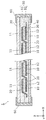
- FIG. 1 is a plan view of the solar cell module according to Embodiment 1.
- FIG. 2 is a cross-sectional view of the solar cell module taken along line II-II in FIG.
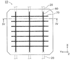
- FIG. 3 is a plan view showing an example of the solar battery cell according to Embodiment 1.
- FIG. 4 is a cross-sectional view showing an example of the solar battery cell according to Embodiment 1.
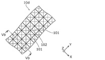
- FIG. 5A is a schematic diagram showing an enlarged plane of the texture structure formed on the silicon substrate according to the first embodiment.
- FIG. 5B is a cross-sectional view of the silicon substrate taken along line Vb-Vb in FIG. 5A.
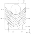
- FIG. 6A is an enlarged cross-sectional view in the broken line region of FIG. FIG.
- FIG. 6B is an enlarged cross-sectional view in the broken line region of FIG. 6A.
- FIG. 7 is a diagram for explaining a radius of curvature representing a round shape of a trough of the first amorphous silicon layer according to the first embodiment.
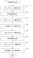
- FIG. 8A is a flowchart showing a method for manufacturing the solar battery cell according to Embodiment 1.
- FIG. 8B is a flowchart showing the method for manufacturing the amorphous silicon layer according to the first embodiment.
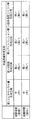
- FIG. 9 is a diagram showing film forming conditions for forming the amorphous silicon layer according to the first embodiment.
- FIG. 10 is an enlarged cross-sectional view of the solar battery cell according to Embodiment 2.
- unevenness called a texture structure is formed on the silicon substrate of the solar battery cell, and an amorphous silicon layer is formed thereon.
- the amorphous silicon layer is composed of an amorphous region (amorphous region) and an epitaxial growth region (crystal region), which are main components of the amorphous silicon layer.
- the amorphous silicon layer is formed such that the epitaxial growth region (crystal region) is thicker than the epitaxial growth region of the inclined portion.
- the epitaxial growth region is more conductive than the amorphous region. Therefore, the higher the occupation ratio of the epitaxial growth region in the amorphous silicon layer, the lower the resistance loss and the curve factor (FF) can be improved.
- the occupation ratio of the epitaxial growth region in the amorphous silicon layer increases, there is a problem that the open circuit voltage (Voc) decreases. Further, when the occupancy ratio of the amorphous region increases, the open circuit voltage increases, but the resistance loss increases and the fill factor decreases.
- the unevenness formed on the silicon substrate is preferably miniaturized (smaller diameter) from the viewpoint of power generation efficiency.
- the texture structure is made finer, the occupation ratio of the epitaxial growth region in the amorphous silicon layer increases. Thereby, since the passivation property of an amorphous silicon layer falls, the open circuit voltage of a photovoltaic cell will fall. That is, power generation efficiency is reduced.
- the film formation rate when the film formation rate is lowered, the quality of the formed film is improved (becomes denser), so that the passivation property of the amorphous silicon layer is improved.
- the film formation rate is lowered in order to form an amorphous silicon layer having high passivation properties, the film is easily affected by the crystal orientation of the silicon substrate during film formation, and epitaxial growth is promoted. That is, when the film formation rate is lowered, the passivation property of the amorphous silicon layer is lowered. Further, when the film formation rate is increased, the epitaxial growth region is not formed. In other words, it has been difficult to control the thickness of the epitaxial growth region with high accuracy in the amorphous silicon layer with high passivation.
- the inventors of the present application have examined whether the above problem can be solved by separating the epitaxial layer including the epitaxial growth region and the amorphous layer having high passivation properties (first passivation layer) and forming them in layers. .
- first passivation layer When the first passivation layer is formed directly on the epitaxial layer, the first passivation layer is epitaxially grown under the influence of the crystal region of the epitaxial layer. That is, the first passivation layer cannot have high passivation properties.
- a first passivation layer having high passivation properties can be formed by providing an amorphous layer (first intermediate layer) having no epitaxial growth region between the epitaxial layer and the first passivation layer.
- the first intermediate layer is a base layer provided so that the first passivation layer is not affected by the crystal region of the epitaxial layer, and is a layer for suppressing epitaxial growth (epitaxial growth suppressing layer).
- the fill factor can be adjusted by controlling the thickness of the epitaxial layer including the epitaxial growth region.
- the adjustment of the thickness of the epitaxial layer can be realized, for example, by managing the film formation time. Therefore, the thickness of the epitaxial layer, that is, the fill factor, can be controlled by simple management such as film formation time.
- the first passivation layer formed on the first intermediate layer is not affected by the epitaxial layer.
- a film can be formed.
- the film formation rate for forming the first passivation layer can be reduced.
- the film quality of the first passivation layer is improved. That is, a first passivation layer having high passivation properties can be formed. Therefore, the open circuit voltage can be improved. As a result, even when the concavo-convex shape of the texture structure is miniaturized, the curve factor and the open circuit voltage can be maintained high.
- the Z-axis direction is, for example, a vertical direction, which is a direction perpendicular to the main surface of the solar cell module and the main surface (surface) of the solar cell.
- the X-axis direction and the Y-axis direction are orthogonal to each other, and both are directions orthogonal to the Z-axis direction.
- “plan view” means viewing from the Z-axis direction.
- FIG. 1 is a plan view of a solar cell module 1 according to the present embodiment.
- FIG. 2 is a cross-sectional view of the solar cell module 1 taken along line II-II in FIG.
- the solar cell module 1 includes a plurality of solar cells 10, a wiring member 20, a surface protection member 30, a back surface protection member 40, a filling member 50, and a frame 60.
- the solar cell module 1 has a structure in which a plurality of solar cells 10 are sealed with a filling member 50 between a front surface protection member 30 and a back surface protection member 40.
- the planar view shape of the solar cell module 1 is, for example, a substantially rectangular shape.
- the solar cell 10 is a photoelectric conversion element (photovoltaic element) that converts light such as sunlight into electric power. As shown in FIG. 1, a plurality of solar cells 10 are arranged in a matrix (matrix shape) on the same plane. Note that the solar cells 10 may be arranged in only one row or one column on the same plane.
- the plurality of solar cells 10 arranged in a straight line form a string (cell string) by connecting two adjacent solar cells 10 with a wiring member 20.
- the plurality of solar cells 10 in one string 10S are electrically connected by the wiring member 20 and are connected in series.
- twelve solar cells 10 arranged at equal intervals along the row direction (X-axis direction) are connected by a wiring member 20 to thereby form one string 10S. Is configured.
- a plurality of strings 10S are formed.
- the plurality of strings 10S (strings) are arranged along the column direction (Y-axis direction).
- the six strings 10S are arranged at equal intervals along the column direction so as to be parallel to each other.
- Each string 10S is connected to another wiring member (not shown) via the wiring member 20.
- a plurality of strings 10S are connected in series or in parallel to form a cell array.
- two adjacent strings 10S are connected in series to form one series connection body (24 solar cells 10 connected in series), and three series connection bodies are provided. It is connected in series, and 72 solar cells are connected in series.
- the plurality of solar cells 10 are arranged with gaps between the solar cells 10 adjacent in the row direction and the column direction.
- a light reflecting member (not shown) may be disposed in the gap.
- the light incident on the gap region between the solar cells 10 is reflected on the surface of the light reflecting member.
- the reflected light is reflected again at the interface between the surface protection member 30 and the external space of the solar cell module 1 and irradiated onto the solar cells 10. Therefore, the photoelectric conversion efficiency of the entire solar cell module 1 can be improved.
- FIG. 3 is a plan view showing an example of the solar battery cell 10 according to the present embodiment.
- the planar view shape of the photovoltaic cell 10 is substantially rectangular shape.
- the solar battery cell 10 has a shape in which a 125 mm square square is missing. That is, one string 10 ⁇ / b> S is configured such that one side of two adjacent solar battery cells 10 faces each other.
- the shape of the photovoltaic cell 10 is not limited to a substantially rectangular shape.
- FIG. 4 is a cross-sectional view showing an example of the solar battery cell 10 according to the present embodiment. Specifically, FIG. 4 is a cross-sectional view of the solar battery cell 10 taken along line IV-IV in FIG. As shown in FIG. 4, the solar cell 10 has a semiconductor pn junction as a basic structure. As an example, one of an n-type single crystal silicon substrate 10d and an n-type single crystal silicon substrate 10d, which is an n-type semiconductor substrate. N-type amorphous silicon layer 10b and n-side electrode 10a sequentially formed on the main surface side of the n-type, and p-type amorphous silicon sequentially formed on the other main surface side of the n-type single crystal silicon substrate 10d.
- the layer 10f and the p-side electrode 10g are configured.
- the n-side electrode 10a and the p-side electrode 10g are, for example, transparent electrodes such as ITO (Indium Tin Oxide).
- an i-type amorphous silicon layer 10c which is a passivation layer, is provided between the n-type single crystal silicon substrate 10d and the n-type amorphous silicon layer 10b.
- An i-type amorphous silicon layer 10e which is a passivation layer, is provided between the crystalline silicon layer 10f. That is, the solar battery cell 10 is, for example, a heterojunction solar battery cell.
- the passivation layer is not limited to the i-type amorphous silicon layers 10c and 10e, and may be a silicon oxide layer, a silicon nitride layer, or the like, or may not be provided.
- the crystalline silicon substrate constituting the solar battery cell 10 is not limited to a single crystal silicon substrate (n-type single crystal silicon substrate or p-type single crystal silicon substrate), but a crystalline silicon substrate such as a polycrystalline silicon substrate. (Hereinafter referred to as a silicon substrate). In the following description, the case where the crystalline silicon substrate is an n-type single crystal silicon substrate will be described.
- the crystalline silicon substrate is simply referred to as a silicon substrate 10d.
- the one main surface of the silicon substrate 10d is the surface (the surface on the Z axis plus side) of the silicon substrate 10d on the main light receiving surface side of the solar cell module 1.
- the other main surface of the silicon substrate 10d is a surface (a surface on the negative side of the Z axis) of the silicon substrate 10d facing away from the one main surface.
- an uneven shape called a texture structure is formed on one main surface (front surface) and the other main surface (back surface) of the silicon substrate 10d.
- One main surface on which the texture structure is formed is a first main surface
- the other main surface is a second main surface.
- the amorphous silicon layers 90 and 91 and the electrodes 10a and 10g formed on the first main surface and the second main surface of the silicon substrate 10d also have an uneven shape reflecting the texture structure.
- the first main surface and the second main surface of the silicon substrate 10d have a texture structure will be described, but the present invention is not limited to this.
- only the first main surface may have the above texture structure.
- the interface between the silicon substrate 10d and the amorphous silicon layer will be described later.
- the solar cell 10 is not limited to the heterojunction type.
- the solar cell 10 may be a crystalline silicon type solar cell such as a single crystal silicon type or a polycrystalline silicon type.
- the thickness of the silicon substrate 10d is 150 ⁇ m or less.
- the solar cell 10 is arranged so that the n-side electrode 10a is on the main light receiving surface side (surface protection member 30 side) of the solar cell module 1, but the present invention is not limited to this.
- the p-side electrode 10g may be arranged on the main light receiving surface side of the solar cell module 1.
- the electrode located on the back side does not need to be transparent, for example, a reflective metal electrode. May be.
- the surface is the surface on the surface protection member 30 side
- the back surface is the surface on the back surface protection member 40 side.
- the front surface collecting electrode 11 and the back surface collecting electrode 12 are formed in the solar battery cell 10.
- the surface collection electrode 11 is electrically connected to the surface side electrode (for example, n side electrode 10a) of the photovoltaic cell 10.
- the back surface collection electrode 12 is electrically connected to the back surface side electrode (for example, p side electrode 10g) of the photovoltaic cell 10.
- Each of the front surface collecting electrode 11 and the back surface collecting electrode 12 is connected to, for example, a plurality of finger electrodes 70 formed linearly so as to be orthogonal to the extending direction of the wiring member 20, and these finger electrodes 70.
- a plurality of bus bar electrodes 80 formed linearly along a direction orthogonal to the finger electrodes 70 (extending direction of the wiring member 20).
- the number of bus bar electrodes 80 is the same as that of the wiring member 20, and is three in the present embodiment.
- the front collector electrode 11 and the rear collector electrode 12 have the same shape as each other, but are not limited thereto. As shown in FIG. 3, when the surface collector electrode 11 is configured, the wiring member 20 is bonded on each of the bus bar electrodes 80. Details of the wiring member 20 will be described later.
- the front collector electrode 11 and the rear collector electrode 12 are made of a low resistance conductive material such as silver (Ag).
- the front collector electrode 11 and the rear collector electrode 12 can be formed by screen printing a conductive paste (silver paste or the like) in which a conductive filler such as silver is dispersed in a binder resin in a predetermined pattern.
- the solar battery cell 10 configured in this way has both the front surface and the back surface as light receiving surfaces.
- carriers are generated in the photoelectric conversion part of the solar battery cell 10.
- the generated carriers are collected by the front surface collecting electrode 11 and the back surface collecting electrode 12 and flow into the wiring member 20.
- carriers generated in the solar battery cell 10 can be efficiently taken out to an external circuit.
- the wiring member 20 is a tab wiring which electrically connects two adjacent photovoltaic cells 10 in the string 10S.
- the two adjacent photovoltaic cells 10 are connected by the three wiring members 20 arrange
- Each wiring member 20 is extended along the alignment direction of the two photovoltaic cells 10 to be connected.
- one end of the wiring member 20 is disposed on the surface of one of the two adjacent solar cells 10, and the other of the wiring members 20. The end portion is disposed on the back surface of the other solar battery cell 10 of the two adjacent solar battery cells 10.
- Each wiring member 20 electrically connects the front surface collector electrode 11 of one solar cell 10 and the back surface collector electrode 12 of the other solar cell 10 in two adjacent solar cells 10.
- the wiring member 20 and the front surface collecting electrode 11 of the solar battery cell 10 and the bus bar electrode 80 of the back surface collecting electrode 12 are joined by a conductive adhesive such as a solder material or a resin adhesive.
- the resin adhesive may include conductive particles.
- the wiring member 20 is a long conductive wiring, for example, a ribbon-shaped metal foil.
- the wiring member 20 can be produced by, for example, cutting a metal foil such as a copper foil or a silver foil, which is entirely covered with solder, silver, or the like into a strip shape having a predetermined length.
- the surface protection member 30 is a member that protects the front side surface of the solar cell module 1 and protects the inside of the solar cell module 1 (solar cell 10 or the like) from an external environment such as wind and rain or external impact. As shown in FIG. 2, the surface protection member 30 is disposed on the surface side of the solar cell 10 and protects the light receiving surface on the surface side of the solar cell 10.
- the surface protection member 30 is configured by a translucent member that transmits light in a wavelength band used for photoelectric conversion in the solar battery cell 10.
- the surface protection member 30 is, for example, a glass substrate (transparent glass substrate) made of a transparent glass material, or a resin substrate made of a hard resin material having a film-like or plate-like translucency and water shielding property.
- the back surface protection member 40 is a member that protects the back surface of the solar cell module 1 and protects the inside of the solar cell module 1 from the external environment. As shown in FIG. 2, the back surface protection member 40 is disposed on the back surface side of the solar battery cell 10 and protects the light receiving surface on the back surface side of the solar battery cell 10.
- the back surface protection member 40 is a film-like or plate-like resin sheet made of a resin material such as polyethylene terephthalate (PET) or polyethylene naphthalate (PEN).
- PET polyethylene terephthalate
- PEN polyethylene naphthalate
- the back surface protection member 40 may be an opaque plate or film.
- the back surface protection member 40 is not restricted to an opaque member, and may be a transparent member such as a glass sheet or a glass substrate made of a glass material.
- a filling member 50 is filled between the front surface protection member 30 and the back surface protection member 40.
- the front surface protection member 30, the back surface protection member 40, and the solar battery cell 10 are bonded and fixed by the filling member 50.
- the filling member 50 is filled so as to fill a space between the front surface protection member 30 and the back surface protection member 40.
- the filling member 50 includes a front surface filling member 51 and a back surface filling member 52.
- Each of the surface filling member 51 and the back surface filling member 52 covers the plurality of solar cells 10 arranged in a matrix.
- the plurality of solar cells 10 are entirely covered with the filling member 50 by performing a laminating process (lamination process) while being sandwiched between, for example, a sheet-like surface filling member 51 and a back surface filling member 52.
- the plurality of strings 10S are sandwiched between the surface filling member 51 and the back surface filling member 52, and further above and below the string 10S.
- the surface protection member 30 and the back surface protection member 40 are arranged, and thermocompression bonding is performed in a vacuum at a temperature of 100 ° C. or higher, for example.
- thermocompression bonding the front surface filling member 51 and the back surface filling member 52 are heated and melted to form the filling member 50 that seals the solar battery cell 10.
- the surface filling member 51 before laminating is, for example, a resin sheet made of a resin material such as ethylene vinyl acetate (EVA) or polyolefin, and is disposed between the plurality of solar cells 10 and the surface protection member 30.
- the surface filling member 51 is mainly filled by laminating so as to fill a gap between the solar battery cell 10 and the surface protection member 30.
- the surface filling member 51 is made of a translucent material.
- a transparent resin sheet made of EVA is used as the surface filling member 51 before the lamination process.
- the back surface filling member 52 before the lamination process is a resin sheet made of a resin material such as EVA or polyolefin, and is disposed between the plurality of solar cells 10 and the back surface protection member 40.
- the back surface filling member 52 is mainly filled by laminating so as to fill a gap between the solar battery cell 10 and the back surface protection member 40.
- the solar cell module 1 in the present embodiment may be of a single-sided light receiving method, and in the case of the single-sided light receiving method, the back surface filling member 52 is not limited to a light-transmitting material, but a black material or white You may be comprised with coloring materials, such as material.
- the frame 60 is an outer frame that covers the peripheral edge of the solar cell module 1.
- the frame 60 is, for example, an aluminum frame (aluminum frame) made of aluminum. As shown in FIG. 1, four frames 60 are used, and are attached to each of the four sides of the solar cell module 1.
- the frame 60 is fixed to each side of the solar cell module 1 with an adhesive, for example.
- FIG. 5A is a schematic diagram showing an enlarged plane of the texture structure formed on the silicon substrate 10d according to the present embodiment.
- FIG. 5B is a cross-sectional view of the silicon substrate 10d taken along the line Vb-Vb in FIG. 5A.
- FIG. 5A is a schematic diagram of the texture structure on the first main surface.
- the first main surface of the silicon substrate 10d has a texture structure (unevenness) in which a plurality of pyramids are two-dimensionally arranged.
- the texture structure has a substrate pyramid 102 sandwiched between a quadrangular pyramid substrate top 101 and an adjacent substrate top 101.
- the pyramid surface between the substrate top portion 101 and the substrate valley portion 102 is a (111) plane of silicon crystal.
- the 2nd main surface may also have a texture structure similarly to the 1st main surface.
- the height from the substrate valley 102 to the substrate top 101 is, for example, 1 ⁇ m or more and 10 ⁇ m or less, and the interval between adjacent substrate tops 101 is, for example, 1 ⁇ m or more and 10 ⁇ m or less.
- the height and pitch of the substrate top portion 101 and the substrate valley portion 102 may be random or regular.
- the shape of the texture structure which the 1st main surface and the 2nd main surface of the silicon substrate 10d have may be the same, and are different. Also good. For example, since the angles of light incident on the first main surface and the second main surface are different, the shape of the texture structure may be determined according to the angle of light incident on each main surface.
- FIG. 6A is an enlarged cross-sectional view taken along a broken line area VIa in FIG.
- FIG. 6A is an enlarged cross-sectional view of the laminated structure in the vicinity of the valleys of the silicon substrate 10d, the first amorphous silicon layer 90, and the n-side electrode 10a.
- 6A shows a slope 104 (see FIG. 7) connecting the top (not shown) and the valley 103 (see FIG. 7) of the first amorphous silicon layer 90 and two slopes 104 adjacent to each other. A valley portion 103 sandwiched therebetween is shown.
- FIG. 6B is an enlarged cross-sectional view taken along broken line area VIb in FIG. 6A.
- the first amorphous silicon layer 90 includes an i-type amorphous silicon layer 10c and an n-type amorphous silicon layer 10b.
- i-type amorphous silicon layer 10c has a three-layer structure.
- the first epitaxial layer 120, the first intermediate layer 121, and the first passivation layer 122 are formed in the i-type amorphous silicon layer 10c.
- the first epitaxial layer 120 has an epitaxially grown crystal region 120a and an amorphous region 120b.
- the first intermediate layer 121 and the first passivation layer 122 are configured only by an amorphous region, and have different densities (film densities). More specifically, the density of the first intermediate layer 121 is lower than the density of the first passivation layer 122.
- the density (film density) means the mass per unit volume (for example, 1 cubic centimeter) of each layer.
- the n-type amorphous silicon layer 10b is a passivation layer composed of only an amorphous region.
- the first intermediate layer 121 and the n-type amorphous silicon layer 10b have different densities (film density). More specifically, the density of the first intermediate layer 121 is lower than the density of the n-type amorphous silicon layer 10b.
- the first amorphous silicon layer 90 includes a first epitaxial layer 120 including a crystal region 120a epitaxially grown on the silicon substrate 10d in the valley portion 103, and an amorphous silicon layer formed on the first epitaxial layer 120.
- a type amorphous silicon layer 10b is laminated in a substantially vertical direction (Z-axis plus side direction) from the first main surface of the silicon substrate 10d.
- the first amorphous silicon layer 90 has a concavo-convex shape reflecting the texture structure of the first main surface of the silicon substrate 10d. Further, the n-side electrode 10a also has an uneven shape reflecting the texture structure.
- the first epitaxial layer 120 of the i-type amorphous silicon layer 10c includes a crystalline region 120a and an amorphous (amorphous) region 120b in the valley portion 103.
- the crystal region 120a may include an epitaxial growth region or a fine crystal region reflecting the crystal orientation of the silicon substrate 10d.
- the amorphous region 120b is a region occupied by amorphous material that does not reflect the crystal orientation of the silicon substrate 10d.
- the conductivity of the first epitaxial layer 120 has a dark conductivity of 1.0 ⁇ 10 ⁇ 7 S / cm or more and 1.0 ⁇ 10 ⁇ 5 S / cm or less, and a photoconductivity of 1.0 ⁇ 10 ⁇ 5 S / cm. ⁇ 10 ⁇ 4 S / cm or more and 1.0 ⁇ 10 ⁇ 3 S / cm or less.
- the fall of a fill factor can be suppressed because the 1st epitaxial layer 120 contains the crystal region 120a. Further, the adjustment of the fill factor can be realized by adjusting the thickness of the first epitaxial layer 120. The thickness of the first epitaxial layer 120 can be adjusted by the film formation time. Therefore, even when the texture structure is miniaturized, a decrease in the fill factor can be suppressed by simple control such as adjusting the film formation time of the first epitaxial layer 120. That is, even when the texture structure is refined, the fill factor can be maintained in a high state.
- the occupation ratio of the crystal region 120a and the amorphous region 120b in the first epitaxial layer 120 is not particularly limited.
- the first epitaxial layer 120 may be composed only of the crystal region 120a.
- the first epitaxial layer 120 may be composed of only the crystal region 120a.
- the crystal region 120 a is superior in conductivity to the amorphous region 120 b that is a main component of the first epitaxial layer 120. Therefore, in the first epitaxial layer 120, the higher the occupation ratio of the crystal region 120a, the lower the resistance loss, and the curve factor can be improved.
- the occupation ratio is the ratio of the area of the crystalline region 120a or the amorphous region 120b to the area of the valley 103 of the first epitaxial layer 120 when the solar battery cell 10 is viewed in cross section (viewed from the Y-axis direction). It is.
- FIG. 6B shows an example in which the crystal region 120a passes through the first intermediate layer 121 formed on the first epitaxial layer 120, but the present invention is not limited to this.
- the crystal region 120 a may not penetrate through the first intermediate layer 121.
- the first epitaxial layer 120 includes a crystal region 120a.
- the first intermediate layer 121 is formed so as not to be affected by the crystal region 120a of the first epitaxial layer 120 when it is formed.
- the film formation rate (film formation rate) for forming the first intermediate layer 121 is set higher than the film formation rate for forming the first epitaxial layer 120.
- the film formation speed for forming the first intermediate layer 121 is three times the film formation speed for forming the first epitaxial layer 120. Thereby, the formed first intermediate layer 121 is formed without being affected by the crystal region 120 a of the first epitaxial layer 120.
- the first intermediate layer 121 is formed only of an amorphous region that does not include an epitaxial growth region. Further, since the deposition rate of the first intermediate layer 121 is high, the density of the first intermediate layer 121 is lower than the density of the first epitaxial layer 120.
- the first intermediate layer 121 is an example of a first amorphous layer.
- the first intermediate layer 121 is formed only of an amorphous region. Therefore, when forming the first passivation layer 122, the first passivation layer 122 is formed without being affected by the crystal region 120a of the first epitaxial layer 120. As a result, the first passivation layer 122 is formed only of the amorphous region.
- the first passivation layer 122 is preferably formed at a low film formation rate.
- the deposition rate for forming the first passivation layer 122 is lower than the deposition rate for forming the first epitaxial layer 120.
- the density of the first passivation layer 122 is higher than the density of the first epitaxial layer 120.
- the electrical conductivity of the 1st passivation layer 122 becomes high by making the film-forming speed
- the conductivity of the first passivation layer 122 can be increased to that of the first intermediate layer 121. It becomes higher than the conductivity.
- the first intermediate layer 121 has a dark conductivity of 1.0 ⁇ 10 ⁇ 14 S / cm or more and 1.0 ⁇ 10 ⁇ 10 S / cm or less, and a photoconductivity of 1.0 ⁇ 10 6.
- the conductivity of the first passivation layer 122 is such that the dark conductivity is 1.0 ⁇ 10 ⁇ 9 S / cm or more and 1.0 ⁇ 10 ⁇ 7 S / cm or less, and the photoconductivity is 1.0. ⁇ 10 ⁇ 7 S / cm or more and 1.0 ⁇ 10 ⁇ 4 S / cm or less. That is, by forming the first passivation layer 122, it is possible to maintain high passivation properties and to suppress a reduction in the fill factor. Therefore, even when the texture structure is miniaturized, it is possible to suppress the decrease of the fill factor and maintain the open circuit voltage at a high level.
- the first intermediate layer 121 has a lower conductivity than the first epitaxial layer 120 and the first passivation layer 122, for example. That is, the resistance loss due to the first intermediate layer 121 is large. For this reason, if the first intermediate layer 121 is thick, the fill factor of the solar battery cell 10 is reduced. Therefore, it is preferable that the first intermediate layer 121 be formed thin.
- the first intermediate layer 121 is preferably formed as thin as possible within the thickness that allows the first passivation layer 122 to be formed without being affected by the first epitaxial layer 120.
- the thickness of the first intermediate layer 121 is smaller than the thickness of the first passivation layer 122.
- the thickness of the first intermediate layer 121 is 1 nm or more and 3 nm or less. Note that the thickness can be adjusted by the time of film formation as in the case of the first epitaxial layer 120.
- the first passivation layer 122 is formed of only an amorphous region. Therefore, when the n-type amorphous silicon layer 10b is formed, the n-type amorphous silicon layer 10b is formed without being affected by the crystal region 120a of the first epitaxial layer 120. Thereby, the n-type amorphous silicon layer 10b is formed only by the amorphous region.
- the n-type amorphous silicon layer 10b is preferably formed at a low film formation rate, like the first passivation layer 122.
- the first passivation layer 122 and the n-type amorphous silicon layer 10b are examples of the second amorphous layer.
- the second amorphous layer is an amorphous silicon layer formed on the first intermediate layer. Note that the n-type amorphous silicon layer 10b may not be included in the second amorphous layer.
- the first amorphous silicon layer 90 is substantially in an amorphous state in a portion excluding the valley portion 103. That is, the n-type amorphous silicon layer 10b and the i-type amorphous silicon layer 10c (the first epitaxial layer 120, the first intermediate layer 121, and the first passivation layer 122) are substantially amorphous except for the valley portion 103. State.
- FIG. 7 is a diagram for explaining the radius of curvature representing the round shape of the valley 103 of the first amorphous silicon layer 90 according to the present embodiment.
- the valley portion 103 has a round shape reflecting the shape of the substrate valley portion 102 of the silicon substrate 10 d when the solar battery cell 10 is viewed in cross section.
- the valley portion 103 is a region sandwiched between substantially linear inclined portions 104.
- the range of the valley portion 103 is defined as a region sandwiched between points X1 to X4 where the inclination of the inclined surface of the inclined portion 104 changes, as shown in FIG.
- the curvature radius R of the valley 103 is 1 nm or more and 300 nm or less.
- the radius of curvature R of the valley 103 is defined as the radius of a circle C including the curved surface of the valley 103 sandwiched between two points X1 and X2.
- FIG. 8A is a flowchart showing a method for manufacturing solar cell 10 according to the present embodiment.
- the (100) plane of the silicon substrate 10d is anisotropically etched (S10).
- S10 anisotropically etched
- a silicon substrate 10d having a (100) plane is immersed in an etching solution.
- the etching solution contains an alkaline aqueous solution.
- the alkaline aqueous solution contains, for example, at least one of sodium hydroxide (NaOH), potassium hydroxide (KOH), and tetramethylammonium hydroxide (TMAH).
- NaOH sodium hydroxide
- KOH potassium hydroxide
- TMAH tetramethylammonium hydroxide
- a texture structure is formed on the front and back surfaces of the silicon substrate 10d, in which square pyramids having the substrate top portion 101 and the substrate valley portion 102 are two-dimensionally arranged.
- the pyramid surface of the quadrangular pyramid is the (111) plane.
- concentration of the alkaline aqueous solution contained in the etching solution is, for example, 0.1 wt% or more and 10 wt% or less.
- a recess that is recessed inside the silicon substrate 10d is defined as a trough.
- the silicon substrate 10d on which the texture structure is formed is isotropically etched (S20).
- substrate trough part 102 is processed into a round shape (refer FIG. 6A and FIG. 6B).
- This process is specifically use a mixed solution of hydrofluoric acid and (HF) and nitric acid mixed solution of (HNO 3), or hydrofluoric acid (HF) and nitric acid (HNO 3) and acetic acid (CH 3 COOH)
- Wet etching or dry etching using a mixed gas of tetrafluoromethane (CF 4 ) and oxygen (O 2 ) can be applied.
- the radius of curvature of the substrate valley 102 can be adjusted by controlling the mixing ratio of the materials and the processing time.
- the silicon substrate 10d that has undergone the isotropic etching step is immersed in a mixed solution containing hydrofluoric acid (HF) and hydrogen peroxide (H 2 O 2 ) (S30).
- a mixed solution of hydrofluoric acid and hydrogen peroxide by using a mixed solution of hydrofluoric acid and hydrogen peroxide, the surface of the valley portion 102 having a rounded shape is selectively modified.
- the concentration of hydrofluoric acid contained in the mixed solution is preferably 0.1% by weight to 5% by weight, and the concentration of hydrogen peroxide is preferably 0.1% by weight to 5% by weight. More preferably, the concentration of hydrofluoric acid contained in the mixed solution is 0.5 wt% or more and 3 wt% or less, and the concentration of hydrogen peroxide is 2 wt% or more and 4 wt% or less.
- step S30 may be omitted.
- an amorphous layer forming step of forming the first amorphous silicon layer 90 and the second amorphous silicon layer 91 on the first main surface and the second main surface of the surface-treated silicon substrate 10d (S40). Is done.
- the amorphous silicon layer having the above-described film structure in the valley portion 103 is formed only on the amorphous silicon layer 90
- the following steps are performed only on the first main surface.
- a vapor phase growth method using a raw material gas containing silicon is formed on the first main surface of the silicon substrate 10d having a texture structure in which a plurality of pyramids are two-dimensionally arranged.
- the first amorphous silicon layer 90 having an uneven shape reflecting the texture structure is formed.
- the i-type amorphous silicon layer 10c (first epitaxial layer 120, first intermediate layer 121 and first passivation layer 122), n-type amorphous silicon layer 10b, i-type amorphous silicon layer 10e, Then, the p-type amorphous silicon layer 10f is formed in this order. Note that the formation order is not limited to this. For example, after the i-type amorphous silicon layer 10c and the i-type amorphous silicon layer 10e are simultaneously formed, the n-type amorphous silicon layer 10b and the p-type amorphous silicon layer 10f may be formed in this order. Good.
- a first epitaxial layer forming step (S41) for forming the first epitaxial layer 120 on the first main surface of the silicon substrate 10d is performed.
- the first epitaxial layer 120 is formed by plasma enhanced chemical vapor deposition (PECVD), Cat-CVD (Catalytic Chemical Vapor Deposition), sputtering, or the like.
- PECVD may use any technique such as RF plasma CVD, high-frequency VHF plasma CVD, or microwave plasma CVD.
- the first epitaxial layer 120 is formed using an RF plasma CVD method.
- a gas obtained by diluting a silicon-containing gas such as silane (SiH 4 ) with hydrogen is supplied to the film-forming chamber, and RF frequency power is applied to the parallel plate electrodes disposed in the film-forming chamber. Is turned into plasma. By supplying this plasma gas to the first main surface of the silicon substrate 10d heated to 150 ° C. or higher and 250 or lower, the first epitaxial layer 120 is formed.
- the film formation rate is adjusted by, for example, the flow rate of the supplied gas. For example, when the flow rate is increased, the film formation rate can be increased.
- the method for adjusting the deposition rate is not limited to this.
- the temperature may be adjusted by the temperature of the silicon substrate 10d, the pressure in the deposition chamber, the RF power, and the like. For example, when the temperature of the silicon substrate 10d, the pressure in the deposition chamber, and the RF power are increased, the deposition rate can be increased.
- the first passivation layer 122 is formed on the first intermediate layer 121.
- a first passivation layer forming step (S43) to be formed is performed.
- the first epitaxial layer 120, the first intermediate layer 121, and the first passivation layer 122 are formed in the i-type amorphous silicon layer 10c. Therefore, in the first intermediate layer forming step for forming the first intermediate layer 121 and the first passivation layer forming step for forming the first passivation layer 122, the film forming method and the material used are the first epitaxial layer forming step. Is the same. What is different from the first epitaxial layer forming step is a film forming condition.
- the first intermediate layer forming step (S42) for forming the first intermediate layer 121 will be described.
- the film formation rate for forming the first intermediate layer 121 is increased, only an amorphous region is formed in the first intermediate layer 121.
- the film formation rate is lowered, a crystal region including an epitaxial growth region is formed in the first intermediate layer 121 due to the influence of the crystal region 120 a of the first epitaxial layer 120. Therefore, the first intermediate layer 121 is formed at a film formation rate at which only an amorphous region is formed.
- the film formation rate for forming the first intermediate layer 121 is 3 ⁇ / second or more and 5 ⁇ / second or less.
- the first intermediate layer forming step is an example of a first amorphous layer forming step.
- the first passivation layer forming step (S43) for forming the first passivation layer 122 will be described.
- the first passivation layer 122 only an amorphous region is formed regardless of the deposition rate. This is because the first passivation layer 122 is formed on the first intermediate layer 121 formed only of the amorphous region. That is, since the first intermediate layer 121 is formed, the first passivation layer 122 is formed without being affected by the crystal region 120 a of the first epitaxial layer 120. Note that a film with better film quality is formed when the film formation rate is lower, so that the film formation rate of the first passivation layer 122 is preferably lower. Thereby, the first passivation layer 122 having high passivation properties is formed.
- the deposition rate for forming the first passivation layer 122 is not less than 0.1 ⁇ / second and not more than 5 ⁇ / second.
- the density (film density) of the first passivation layer 122 formed at the film formation speed is 2.2 g / cm 3 or more and 2.4 g / cm 3 or less.
- the hydrogen concentration is 1 ⁇ 10 21 / cm 3 or more and 5 ⁇ 10 22 / cm 3 or less.
- the thickness of the first passivation layer 122 is controlled by the film formation time. By increasing the film formation time, the thickness of the first passivation layer 122 can be increased.
- the thickness of the first passivation layer 122 is not particularly limited. For example, it is formed thicker than the first intermediate layer 121.
- the film formation time for forming the first passivation layer 122 is appropriately determined according to the film formation speed for forming the first passivation layer 122 and the target thickness of the first passivation layer 122.
- the target thickness is, for example, a target value of the thickness of the first passivation layer 122 for obtaining a desired open circuit voltage.
- the thickness of the 1st passivation layer 122 is 1 nm or more and 25 nm or less, for example.
- the thickness of the first passivation layer 122 is the thickness of the first passivation layer 122 in the valley portion 103 in the Z-axis direction and corresponds to the thickness T3 shown in FIG. 6A.
- the thickness of the first intermediate layer 121 is thinner than the thickness of the first passivation layer 122 has been described.
- the present invention is not limited to this.
- the thickness of the first passivation layer 122 may be the same as or thinner than the thickness of the first intermediate layer 121 as long as a desired open circuit voltage can be obtained. That is, the thickness of the first intermediate layer 121 may be larger than the thickness of the first passivation layer 122.
- an n-type amorphous silicon layer forming step (S44) for forming the n-type amorphous silicon layer 10b on the first passivation layer 122 is performed.
- the n-type amorphous silicon layer 10b is formed by PECVD, Cat-CVD, sputtering, or the like.
- an RF plasma CVD method is applied. Specifically, a mixed gas obtained by diluting a silicon-containing gas such as silane (SiH 4 ) and an n-type dopant-containing gas such as phosphine (PH 3 ) with hydrogen is supplied to the film forming chamber, and is disposed in the film forming chamber.
- RF high frequency power is applied to the parallel plate electrodes, and the mixed gas is turned into plasma.
- the n-type amorphous silicon layer 10b is formed on the first passivation layer 122 by supplying the plasma gas to the first main surface of the silicon substrate 10d heated to 150 ° C. or more and 250 ° C. or less. It is formed.
- the n-type amorphous silicon layer 10b In the n-type amorphous silicon layer 10b, only an amorphous region is formed regardless of the deposition rate. This is because the n-type amorphous silicon layer 10b is formed on the first passivation layer 122 formed only by the amorphous region. In addition, since a film with better film quality is formed when the film formation rate is lower, it is preferable that the film formation rate of the n-type amorphous silicon layer 10b is lower. Thereby, the n-type amorphous silicon layer 10b having high passivation properties is formed. For example, the deposition rate for forming the n-type amorphous silicon layer 10b is not less than 0.1 ⁇ / second and not more than 5 ⁇ / second.
- the density (film density) of the n-type amorphous silicon layer 10b formed at the deposition rate is 2.2 g / cm 3 or more and 2.4 g / cm 3 or less.
- the hydrogen concentration is 1 ⁇ 10 21 / cm 3 or more and 5 ⁇ 10 22 / cm 3 or less.
- the thickness of the n-type amorphous silicon layer 10b is controlled by the film formation time. By increasing the deposition time, the thickness of the n-type amorphous silicon layer 10b can be increased.
- the thickness of the n-type amorphous silicon layer 10b is not particularly limited.
- the first passivation layer 122 is formed with the same thickness.
- the film formation time for forming the n-type amorphous silicon layer 10b depends on the film formation speed for forming the n-type amorphous silicon layer 10b and the target thickness of the n-type amorphous silicon layer 10b. Is determined as appropriate.
- the target thickness is, for example, a target value of the thickness of the n-type amorphous silicon layer 10b for obtaining a desired open circuit voltage. Further, the thickness of the n-type amorphous silicon layer 10b is, for example, not less than 1 nm and not more than 25 nm. The thickness of the n-type amorphous silicon layer 10b is the thickness of the n-type amorphous silicon layer 10b in the valley portion 103 in the Z-axis direction and corresponds to the thickness T4 shown in FIG. 6A.
- the film formation rate in the first intermediate layer formation step is higher than the film formation rate in the first epitaxial layer formation step.
- the film formation rate in the first intermediate layer formation step is three times the film formation rate in the first epitaxial layer formation step.
- the first intermediate layer 121 is formed only from the amorphous region without being affected by the first epitaxial layer 120.
- the film formation rate in the first passivation layer forming step and the n-type amorphous silicon layer forming step is lower than the film formation rate in the first intermediate layer forming step.
- the first passivation layer 122 and the n-type amorphous silicon layer 10b have a higher density and better film quality than the first intermediate layer 121. That is, the first passivation layer 122 and the n-type amorphous silicon layer 10b have high passivation properties and high conductivity. Therefore, the first passivation layer 122 and the n-type amorphous silicon layer 10b can suppress the reduction of the fill factor in the first amorphous silicon layer 90 and maintain the open circuit voltage at a high level.
- the film formation rate in the first epitaxial layer formation step is higher than the film formation rate in the first passivation layer formation step and lower than the film formation rate in the first intermediate layer formation step, for example. That is, the density of the first epitaxial layer 120 is higher than the density of the first intermediate layer 121 and lower than the density of the first passivation layer 122.
- the first epitaxial layer 120 both the crystal region 120a including the epitaxial growth region and the amorphous region 120b are formed. That is, a decrease in open circuit voltage due to the crystal region 120a can be suppressed by the amorphous region 120b.
- the film formation rate in the first epitaxial layer formation step is lower than the film formation rate in the first intermediate layer formation step.
- the crystal region 120a is easily formed.
- the crystal region 120a formed in the first epitaxial layer 120 can maintain the fill factor of the first amorphous silicon layer 90 at a high level.
- the film formation rate in the first epitaxial layer formation step may be lower than the film formation rate in the first passivation layer formation step.
- the film formation rate in the first epitaxial layer formation step may be lower than the film formation rate in the n-type amorphous silicon formation step.
- the film formation time in the first intermediate layer formation step is shorter than the film formation time in the first passivation layer formation step.
- the thickness of the first intermediate layer 121 is formed thinner than the thickness of the first passivation layer 122. Since the first intermediate layer 121 has a large resistance loss, the first intermediate layer 121 is formed thin, so that a decrease in the fill factor due to the formation of the first intermediate layer 121 can be suppressed.
- the film formation time in the first epitaxial layer formation step is longer than the film formation time in the first intermediate layer formation step, and the film formation in the first passivation layer formation step and the n-type amorphous silicon layer formation step.
- the film formation time in the first epitaxial layer formation step may be shorter than the film formation time in the first intermediate layer formation step, or may be shorter than the film formation time in the first passivation layer formation step and the n-type amorphous silicon layer formation step. It may be long.
- the film formation time in the first epitaxial layer formation step is appropriately determined according to the film formation rate in the first epitaxial layer formation step and the target thickness of the first epitaxial layer 120.
- step S10 a texture structure in which a plurality of pyramids are two-dimensionally arranged in step S10 is formed on the second main surface.
- the illustration of the second epitaxial layer, the second intermediate layer, and the second passivation layer formed on the second main surface is omitted.
- the second epitaxial layer, the second intermediate layer, and the second passivation layer are formed of the i-type amorphous silicon layer 10e.
- a second epitaxial layer forming step (S45) for forming a second epitaxial layer including an epitaxial growth region on the second main surface of the silicon substrate 10d is performed.
- the method for forming the second epitaxial layer is the same as the method for forming the first epitaxial layer 120 (step S41), and the description thereof is omitted.
- the density and thickness of the second epitaxial layer may be changed from the density and thickness of the first epitaxial layer 120. In the case of changing, adjustment is made by the film formation speed and the film formation time.
- the second epitaxial layer is formed of the same material as the first epitaxial layer 120.
- a layer forming step (S47) is performed.
- the second epitaxial layer, the second intermediate layer, and the second passivation layer are formed in the i-type amorphous silicon layer 10e. Therefore, in the second intermediate layer forming step for forming the second intermediate layer and the second passivation layer forming step for forming the second passivation layer, the film forming method and the material used are the same as those in the second epitaxial layer forming step. .
- the concentration of diborane (B 2 H 6 ) in the mixed gas is, for example, 1%.
- the p-type amorphous silicon layer 10f In the p-type amorphous silicon layer 10f, only an amorphous region is formed regardless of the deposition rate. This is because the p-type amorphous silicon layer 10f is formed on the second passivation layer formed only of the amorphous region. In addition, since the film
- the second passivation layer and the p-type amorphous silicon layer 10f are an example of a fourth amorphous layer.
- the second amorphous silicon layer 91 is a second epitaxial layer including a crystal region epitaxially grown on the silicon substrate 10d and an amorphous silicon layer formed on the second epitaxial layer in the concave and convex valleys.
- Two intermediate layers, a second passivation layer that is an amorphous silicon layer formed on the second intermediate layer, and a p-type amorphous silicon layer that is an amorphous silicon layer formed on the second passivation layer 10f are stacked in a substantially vertical direction (Z-axis minus side direction) from the second main surface of the silicon substrate 10d.
- the density of the second intermediate layer is lower than the densities of the second passivation layer and the p-type amorphous silicon layer 10f.
- amorphous silicon layers 90 and 91 are formed on the first main surface and the second main surface of the silicon substrate 10d.
- the n-side electrode 10a and the p-side electrode 10g which are transparent electrodes, and the surface collector electrode 11 and the back surface which are metal electrodes
- the collector electrode 12 is formed (S50).
- the n-side electrode 10a is formed on the n-type amorphous silicon layer 10b
- the p-side electrode 10g is formed on the p-type amorphous silicon layer 10f.
- a transparent conductive oxide such as indium tin oxide (ITO) is formed on the n-type amorphous silicon layer 10b and the p-type amorphous silicon layer 10f by vapor deposition or sputtering. Film.
- the solar battery cell 10 according to the present embodiment is formed.
- the second amorphous layer is formed in the first passivation layer 122 and the n-type amorphous silicon layer 10b.
- a part of the second amorphous layer has the same conductivity type as that of the silicon substrate 10d (n-type single crystal silicon substrate).
- the passivation layer is formed only in the n-type amorphous silicon layer 10b, the second amorphous has the same conductivity type as that of the silicon substrate 10d.
- the second amorphous silicon layer 91 having a conductivity type different from that of the silicon substrate 10d carriers are effectively separated at the pn junction that is the interface. Therefore, the importance of considering the resistance loss at the pn junction is low. Therefore, the second amorphous silicon layer 91 having a conductivity type different from that of the silicon substrate 10 d is preferably formed so that the second epitaxial layer is thinner than the first epitaxial layer 120. Further, the second amorphous silicon layer 91 may not have the second epitaxial layer. That is, the i-type amorphous silicon layer 10e may be formed of only an amorphous region.
- the first amorphous silicon layer 90 having the same conductivity type as that of the silicon substrate 10d improves the fill factor and reduces the open circuit voltage by reducing the resistance loss.
- the open-circuit voltage can be effectively improved by the second amorphous silicon layer 91 having a conductivity type different from that of the silicon substrate 10d.
- Solar cell 10 is formed on a first main surface of silicon substrate 10d having a texture structure in which a plurality of pyramids are two-dimensionally arranged on a first main surface, and on the first main surface of silicon substrate 10d, A first amorphous silicon layer 90 having a concavo-convex shape reflecting the texture structure.
- the first amorphous silicon layer 90 includes a first epitaxial layer 120 including a crystal region 120 a epitaxially grown on the silicon substrate 10 d and an amorphous formed on the first epitaxial layer 120 in the concave and convex valley 103.
- a first amorphous layer (first intermediate layer 121) which is a silicon layer, and a second amorphous layer (first passivation layer 122 and n-type amorphous silicon) which is an amorphous silicon layer formed on the first amorphous layer.
- Layer 10b in this order.
- the density of the first amorphous layer is lower than the density of the second amorphous layer.
- the solar cell 10 of the present invention includes a first epitaxial layer 120 including a crystal region 120a epitaxially grown in a concave and convex valley 103 on a first main surface, and a first amorphous layer (first layer) that is an amorphous silicon layer.
- the intermediate layer 121) and the second amorphous layer are formed in this order.
- the resistance loss in the first amorphous silicon layer 90 is reduced, and the fill factor (FF) of the solar battery cell 10 can be improved.
- the first intermediate layer 121 is formed so as to have a density lower than that of the first passivation layer 122 and the n-type amorphous silicon layer 10b, so that the first intermediate layer 121 is formed without being affected by the crystal region 120a of the first epitaxial layer 120. Is done. That is, the first intermediate layer 121 has only an amorphous region.
- the first passivation layer 122 and the n-type amorphous silicon layer 10b are formed on the first intermediate layer 121 having only an amorphous region, the first passivation layer 122 and the n-type amorphous silicon layer 10b are affected by the crystal region 120a of the first epitaxial layer 120. Formed without. That is, the first passivation layer 122 and the n-type amorphous silicon layer 10b have only an amorphous region. Thereby, the open circuit voltage (Voc) in the first amorphous silicon layer 90 can be improved. Further, the density of the first intermediate layer 121 is lower than the densities of the first passivation layer 122 and the n-type amorphous silicon layer 10b.
- the density of the first passivation layer 122 and the n-type amorphous silicon layer 10b is high, the first passivation layer 122 and the n-type amorphous silicon layer 10b have high passivation properties and high conductivity. Thereby, the fall of the fill factor by the 1st passivation layer 122 and the n-type amorphous silicon layer 10b can be suppressed, and the open circuit voltage in the 1st amorphous silicon layer 90 can be improved further.
- the fill factor and the open circuit voltage can be maintained high.
- the thickness of the first intermediate layer 121 is thinner than the thickness of the first passivation layer 122 and the n-type amorphous silicon layer 10b.
- the first intermediate layer 121 has lower conductivity and higher resistance loss than the first passivation layer 122 and the n-type amorphous silicon layer 10b.
- resistance loss due to the first intermediate layer 121 can be suppressed. That is, it is possible to suppress a decrease in the fill factor due to the first intermediate layer 121.
- the thickness of the first intermediate layer 121 is not less than 1 nm and not more than 3 nm.
- the first passivation layer 122 formed on the first intermediate layer 121 is formed without being affected by the crystal region 120 a of the first epitaxial layer 120. Moreover, the resistance loss by the 1st intermediate
- the first epitaxial layer 120 further has an amorphous region 120b.
- the open-circuit voltage in the first epitaxial layer 120 can be improved. Thereby, the fall of the open circuit voltage by the crystal
- the density of the first epitaxial layer 120 is higher than the density of the first intermediate layer 121.
- At least one part of the first epitaxial layer 120, the first amorphous layer (first intermediate layer 121), and the second amorphous layer (first passivation layer 122 and n-type amorphous silicon layer 10b) is a silicon substrate.
- the resistance loss is further reduced, and the fill factor can be improved.
- the first amorphous silicon layer 90 and the second amorphous silicon layer 91 it is possible to improve the fill factor while suppressing a decrease in the open-circuit voltage.
- the unevenness reflecting the texture structure by the vapor phase growth method using the raw material gas containing silicon on the first main surface of the silicon substrate 10d having the texture structure is included.
- An amorphous layer forming step (S40) for forming the first amorphous silicon layer 90 having a shape is included.
- the amorphous layer forming step includes a first epitaxial layer forming step (S41), a first intermediate layer forming step (S42), a first passivation layer forming step (S43), and an n-type amorphous silicon layer. Forming step (S44).
- the first epitaxial layer 120 including the crystal region 120a formed on the silicon substrate 10d and epitaxially grown is formed.
- the first intermediate layer forming step (S42) the first intermediate layer 121, which is an amorphous silicon layer formed on the first epitaxial layer 120, is formed.
- the first passivation layer forming step (S43) a first passivation layer 122 that is an amorphous silicon layer formed on the first intermediate layer 121 is formed.
- the n-type amorphous silicon layer forming step (S44) an n-type amorphous silicon layer 10b, which is an amorphous silicon layer formed on the first passivation layer 122, is formed.
- the film formation rate in the first intermediate layer formation step is higher than the film formation rate in the first passivation layer formation step and the n-type amorphous silicon layer formation step.
- the first epitaxial layer 120 including the crystal region 120a that has been epitaxially grown and the first intermediate layer 121 that is an amorphous silicon layer in the concave and convex valley portion 103 on the first main surface.
- the first passivation layer 122 and the n-type amorphous silicon layer 10b are formed in this order.
- the resistance loss in the first amorphous silicon layer 90 is reduced, and the fill factor (FF) of the solar battery cell can be improved.
- the film formation rate in the first intermediate layer formation step is higher than the film formation rate in the first passivation layer formation step and the n-type amorphous silicon layer formation step, so that the first intermediate layer 121 is a crystalline region of the first epitaxial layer 120. It is formed without being affected by 120a. That is, the first intermediate layer 121 has only an amorphous region.
- the first passivation layer 122 is formed on the first intermediate layer 121 having only an amorphous region, so that the first passivation layer 122 is formed without being influenced by the crystal region 120a of the first epitaxial layer 120. That is, the first passivation layer 122 has only an amorphous region.
- the first intermediate layer 121 is the first passivation layer.
- 122 and the n-type amorphous silicon layer 10b are formed with a lower density. That is, the first passivation layer 122 has high passivation properties and high conductivity. Thereby, the fall of the fill factor by the 1st passivation layer 122 and the n-type amorphous silicon layer 10b can be suppressed, and the open circuit voltage in the 1st amorphous silicon layer 90 can be improved further.
- the method for manufacturing a solar battery cell according to the present embodiment even when the texture structure formed in the solar battery cell is miniaturized, the curve factor and the open circuit voltage can be maintained high.
- the first intermediate layer 121 is formed thinner than the first passivation layer 122 and the n-type amorphous silicon layer 10b. Therefore, resistance loss due to the first intermediate layer 121 can be suppressed. That is, it is possible to suppress a decrease in the fill factor due to the first intermediate layer 121.
- the film formation rate in the first epitaxial layer formation step (S41) is higher than the film formation rate in the first passivation layer formation step (S43) and the n-type amorphous silicon layer formation step (S44), and the first intermediate layer is formed. It is lower than the film formation rate in the layer formation step (S42).
- both the crystalline region 120a and the amorphous region 120b including the epitaxial growth region are formed in the first epitaxial layer 120. That is, a decrease in open circuit voltage due to the crystal region 120a can be suppressed by the amorphous region 120b. Therefore, according to the manufacturing method of the photovoltaic cell which concerns on this Embodiment, a fall to an open circuit voltage can be suppressed and a curve factor can be maintained in a high state.
- FIG. 10 is an enlarged cross-sectional view of solar cell 210 according to the present embodiment.
- the first epitaxial layer 120, the first intermediate layer 121, the first passivation layer 122, and the n-type amorphous silicon layer 10b are formed in the valley portion 103 has been described.
- the entire region of first amorphous silicon layer 90 having an uneven shape reflecting the texture structure formed on silicon substrate 10d is substantially from the first main surface of silicon substrate 10d.
- a first epitaxial layer 120, a first intermediate layer 121, a first passivation layer 122, and an n-type amorphous silicon layer 10b are formed in this order in the vertical direction.
- the valley portion 103 is also included in the entire region of the first amorphous silicon layer 90. That is, in all of the top portion 105, the valley portion 103, the top portion 105, and the inclined portion 104 connecting the valley portion 103 of the first amorphous silicon layer 90 having the uneven shape, the first epitaxial layer 120, the first intermediate layer 121, the first One passivation layer 122 and n-type amorphous silicon layer 10b are formed in this order.
- the first epitaxial layer 120, the first intermediate layer 121, and the first passivation layer 122 are formed in the i-type amorphous silicon layer 10c. Further, a passivation layer is formed in the n-type amorphous silicon layer 10b.
- the first intermediate layer 121 is an example of a first amorphous layer
- the first passivation layer 122 and the n-type amorphous silicon layer 10b are examples of a second amorphous layer.
- FIG. 10 illustrates an example in which the first epitaxial layer 120, the first intermediate layer 121, the first passivation layer 122, and the n-type amorphous silicon layer 10b are formed with a substantially constant thickness over the entire texture structure.
- the thickness of the first epitaxial layer 120 may be increased in the valley portion 103.
- FIG. 10 illustrates each layer formed over the entire first main surface of the silicon substrate 10d, the second epitaxial layer, the second intermediate layer, and the second passivation are also formed over the entire second main surface of the silicon substrate 10d.
- a layer and a p-type amorphous silicon layer 10f may be formed. Note that the second epitaxial layer may not be formed.
- the first amorphous silicon layer 90 in the solar battery cell 210 according to the present embodiment has a first epitaxial layer 120, a first amorphous layer (first intermediate layer 121), and an uneven shape including the valley portion 103.
- the second amorphous layer (the first passivation layer 122 and the n-type amorphous silicon layer 10b) is provided in this order.
- the first amorphous silicon layer 90 has been described as being composed of the n-type amorphous silicon layer 10b and the i-type amorphous silicon layer 10c, the present invention is not limited to this.
- the first amorphous silicon layer 90 may be composed only of the n-type amorphous silicon layer 10b.
- the first epitaxial layer 120, the first intermediate layer 121, and the first passivation layer 122 are formed in the n-type amorphous silicon layer 10b.
- the materials used for film formation are the same, and the first epitaxial layer 120, the first intermediate layer 121, and the first material are changed by changing the film formation speed for forming the n-type amorphous silicon layer 10b.
- a passivation layer 122 is formed.
- the present invention is not limited to this.
- the layer structures of the amorphous silicon layers 90 and 91 formed on the first main surface and the second main surface may be different.
- the first epitaxial layer 120, the first intermediate layer 121, and the first passivation layer 122 are formed in the i-type amorphous silicon layer 10c, and the passivation layer is formed in the n-type amorphous silicon layer 10b. It is formed.
- the second epitaxial layer and the second intermediate layer may be formed in the i-type amorphous silicon layer 10e, and the passivation layer may be formed in the p-type amorphous silicon layer 10f.
- Other layer structures may also be used.
- the solar cell module 1 a configuration in which a plurality of solar cells are arranged in a matrix on the surface is shown, but the present invention is not limited to this.
- the solar cells may be arranged in an annular shape or in a one-dimensional linear or curved shape.
- the solar cell shown above can be used regardless of the size of the texture structure as long as it has a texture structure.
- the embodiment can be realized by arbitrarily combining the components and functions in each embodiment without departing from the scope of the present invention, or a form obtained by subjecting each embodiment to various modifications conceived by those skilled in the art. Forms are also included in the present invention.
Landscapes
- Photovoltaic Devices (AREA)
- Life Sciences & Earth Sciences (AREA)
- Engineering & Computer Science (AREA)
- Sustainable Energy (AREA)
- Sustainable Development (AREA)
Abstract
La présente invention concerne une cellule solaire (10) qui comprend : un substrat de silicium (10d) ayant une structure texturée sur une première surface principale ; et une première couche de silicium non cristallin (90) ayant une forme présentant des évidements et des saillies reflétant la structure texturée, la première couche de silicium non cristallin (90) étant formée sur la première surface principale du substrat de silicium (10d). Dans une partie vallée (103) ayant une forme présentant des évidements et des saillies, la première couche de silicium non cristallin (90) présente, dans cet ordre : une première couche épitaxiale (120) formée par croissance épitaxiale qui comprend une région cristalline (120a) sur le substrat de silicium (10d) ; une première couche amorphe (121) qui est une couche de silicium non cristallin ; et une seconde couche amorphe (122) qui est une couche de silicium non cristallin. De plus, la densité de la première couche amorphe (121) est inférieure à la densité de la seconde couche amorphe (122).
Priority Applications (2)
| Application Number | Priority Date | Filing Date | Title |
|---|---|---|---|
| JP2018542479A JP6745491B2 (ja) | 2016-09-30 | 2017-09-21 | 太陽電池セル、太陽電池モジュール、及び太陽電池セルの製造方法 |
| US16/368,662 US11038071B2 (en) | 2016-09-30 | 2019-03-28 | Solar cell, solar cell module, and method for manufacturing solar cell |
Applications Claiming Priority (2)
| Application Number | Priority Date | Filing Date | Title |
|---|---|---|---|
| JP2016195006 | 2016-09-30 | ||
| JP2016-195006 | 2016-09-30 |
Related Child Applications (1)
| Application Number | Title | Priority Date | Filing Date |
|---|---|---|---|
| US16/368,662 Continuation US11038071B2 (en) | 2016-09-30 | 2019-03-28 | Solar cell, solar cell module, and method for manufacturing solar cell |
Publications (1)
| Publication Number | Publication Date |
|---|---|
| WO2018061966A1 true WO2018061966A1 (fr) | 2018-04-05 |
Family
ID=61760422
Family Applications (1)
| Application Number | Title | Priority Date | Filing Date |
|---|---|---|---|
| PCT/JP2017/034056 Ceased WO2018061966A1 (fr) | 2016-09-30 | 2017-09-21 | Cellule solaire, module de cellule solaire et procédé de fabrication de cellule solaire |
Country Status (3)
| Country | Link |
|---|---|
| US (1) | US11038071B2 (fr) |
| JP (1) | JP6745491B2 (fr) |
| WO (1) | WO2018061966A1 (fr) |
Families Citing this family (1)
| Publication number | Priority date | Publication date | Assignee | Title |
|---|---|---|---|---|
| JP2023157621A (ja) * | 2022-04-15 | 2023-10-26 | パナソニックホールディングス株式会社 | 太陽電池モジュール |
Citations (4)
| Publication number | Priority date | Publication date | Assignee | Title |
|---|---|---|---|---|
| US20090272435A1 (en) * | 2008-04-30 | 2009-11-05 | General Electric Company | Compositionally-graded and structurally-graded photovoltaic devices and methods of fabricating such devices |
| JP4660561B2 (ja) * | 2007-03-19 | 2011-03-30 | 三洋電機株式会社 | 光起電力装置 |
| JP2014011198A (ja) * | 2012-06-27 | 2014-01-20 | Mitsubishi Electric Corp | 光起電力装置およびその製造方法 |
| WO2014155833A1 (fr) * | 2013-03-28 | 2014-10-02 | 三洋電機株式会社 | Batterie solaire |
Family Cites Families (2)
| Publication number | Priority date | Publication date | Assignee | Title |
|---|---|---|---|---|
| JP2004335823A (ja) * | 2003-05-09 | 2004-11-25 | Canon Inc | 光起電力素子及び光起電力素子の形成方法 |
| KR101909143B1 (ko) * | 2012-01-20 | 2018-10-17 | 엘지전자 주식회사 | 양면 수광형 태양전지 |
-
2017
- 2017-09-21 WO PCT/JP2017/034056 patent/WO2018061966A1/fr not_active Ceased
- 2017-09-21 JP JP2018542479A patent/JP6745491B2/ja active Active
-
2019
- 2019-03-28 US US16/368,662 patent/US11038071B2/en active Active
Patent Citations (4)
| Publication number | Priority date | Publication date | Assignee | Title |
|---|---|---|---|---|
| JP4660561B2 (ja) * | 2007-03-19 | 2011-03-30 | 三洋電機株式会社 | 光起電力装置 |
| US20090272435A1 (en) * | 2008-04-30 | 2009-11-05 | General Electric Company | Compositionally-graded and structurally-graded photovoltaic devices and methods of fabricating such devices |
| JP2014011198A (ja) * | 2012-06-27 | 2014-01-20 | Mitsubishi Electric Corp | 光起電力装置およびその製造方法 |
| WO2014155833A1 (fr) * | 2013-03-28 | 2014-10-02 | 三洋電機株式会社 | Batterie solaire |
Also Published As
| Publication number | Publication date |
|---|---|
| JP6745491B2 (ja) | 2020-08-26 |
| JPWO2018061966A1 (ja) | 2019-04-11 |
| US20190221684A1 (en) | 2019-07-18 |
| US11038071B2 (en) | 2021-06-15 |
Similar Documents
| Publication | Publication Date | Title |
|---|---|---|
| US12278303B1 (en) | Solar cell and photovoltaic module | |
| US9214576B2 (en) | Transparent conducting oxide for photovoltaic devices | |
| US12166142B1 (en) | Solar cell, method for preparing the same, and photovoltaic module | |
| CN116364794A (zh) | 太阳能电池、光伏组件及太阳能电池的制备方法 | |
| CN117712193A (zh) | 太阳能电池及其制备方法、光伏组件 | |
| CN107112376A (zh) | 双层光伏设备 | |
| JP2008235795A (ja) | 太陽電池 | |
| JP7814575B2 (ja) | 太陽電池及び光起電力モジュール | |
| CN115377230A (zh) | 太阳能电池及光伏组件 | |
| JP6664065B2 (ja) | 太陽電池素子および太陽電池モジュール | |
| CN115000198B (zh) | 太阳能电池及光伏组件 | |
| CN115985992A (zh) | 一种n型单晶硅hbc太阳能电池结构及其制备方法 | |
| JP7820075B2 (ja) | 太陽電池及びその製造方法、積層型電池並びに太陽電池モジュール | |
| JP6745491B2 (ja) | 太陽電池セル、太陽電池モジュール、及び太陽電池セルの製造方法 | |
| KR101632451B1 (ko) | 박막 태양 전지 | |
| US20110303270A1 (en) | Solar cell structure having high photoelectric conversion efficiency and method of manufacturing the same | |
| JP2015133341A (ja) | 裏面接合型太陽電池及びその製造方法 | |
| JP2010080885A (ja) | 太陽電池の製造方法 | |
| CN111211187A (zh) | 太阳能单电池和太阳能电池组件 | |
| WO2018003243A1 (fr) | Module à cellules solaires | |
| KR100861548B1 (ko) | 박막형 태양전지와 그의 제조방법 | |
| KR101086260B1 (ko) | 플렉서블 기판 또는 인플렉서블 기판을 포함하는 광기전력 장치 및 광기전력 장치의 제조 방법 | |
| KR101612805B1 (ko) | 박막형 태양전지 모듈 및 그의 제조방법 | |
| US12376415B2 (en) | Solar cell and photovoltaic module | |
| JP2011181544A (ja) | 太陽電池およびその製造方法 |
Legal Events
| Date | Code | Title | Description |
|---|---|---|---|
| 121 | Ep: the epo has been informed by wipo that ep was designated in this application |
Ref document number: 17855921 Country of ref document: EP Kind code of ref document: A1 |
|
| ENP | Entry into the national phase |
Ref document number: 2018542479 Country of ref document: JP Kind code of ref document: A |
|
| NENP | Non-entry into the national phase |
Ref country code: DE |
|
| 122 | Ep: pct application non-entry in european phase |
Ref document number: 17855921 Country of ref document: EP Kind code of ref document: A1 |