WO2018070206A1 - Dispositif spectroscopique et dispositif d'imagerie - Google Patents
Dispositif spectroscopique et dispositif d'imagerie Download PDFInfo
- Publication number
- WO2018070206A1 WO2018070206A1 PCT/JP2017/034067 JP2017034067W WO2018070206A1 WO 2018070206 A1 WO2018070206 A1 WO 2018070206A1 JP 2017034067 W JP2017034067 W JP 2017034067W WO 2018070206 A1 WO2018070206 A1 WO 2018070206A1
- Authority
- WO
- WIPO (PCT)
- Prior art keywords
- light
- scattering plate
- spectroscopic device
- wavelength
- shape
- Prior art date
- Legal status (The legal status is an assumption and is not a legal conclusion. Google has not performed a legal analysis and makes no representation as to the accuracy of the status listed.)
- Ceased
Links
Images





Classifications
-
- G—PHYSICS
- G01—MEASURING; TESTING
- G01J—MEASUREMENT OF INTENSITY, VELOCITY, SPECTRAL CONTENT, POLARISATION, PHASE OR PULSE CHARACTERISTICS OF INFRARED, VISIBLE OR ULTRAVIOLET LIGHT; COLORIMETRY; RADIATION PYROMETRY
- G01J3/00—Spectrometry; Spectrophotometry; Monochromators; Measuring colours
- G01J3/12—Generating the spectrum; Monochromators
- G01J3/18—Generating the spectrum; Monochromators using diffraction elements, e.g. grating
-
- G—PHYSICS
- G01—MEASURING; TESTING
- G01J—MEASUREMENT OF INTENSITY, VELOCITY, SPECTRAL CONTENT, POLARISATION, PHASE OR PULSE CHARACTERISTICS OF INFRARED, VISIBLE OR ULTRAVIOLET LIGHT; COLORIMETRY; RADIATION PYROMETRY
- G01J3/00—Spectrometry; Spectrophotometry; Monochromators; Measuring colours
- G01J3/02—Details
- G01J3/0205—Optical elements not provided otherwise, e.g. optical manifolds, diffusers, windows
-
- G—PHYSICS
- G01—MEASURING; TESTING
- G01J—MEASUREMENT OF INTENSITY, VELOCITY, SPECTRAL CONTENT, POLARISATION, PHASE OR PULSE CHARACTERISTICS OF INFRARED, VISIBLE OR ULTRAVIOLET LIGHT; COLORIMETRY; RADIATION PYROMETRY
- G01J3/00—Spectrometry; Spectrophotometry; Monochromators; Measuring colours
- G01J3/02—Details
- G01J3/0205—Optical elements not provided otherwise, e.g. optical manifolds, diffusers, windows
- G01J3/021—Optical elements not provided otherwise, e.g. optical manifolds, diffusers, windows using plane or convex mirrors, parallel phase plates, or particular reflectors
-
- G—PHYSICS
- G01—MEASURING; TESTING
- G01J—MEASUREMENT OF INTENSITY, VELOCITY, SPECTRAL CONTENT, POLARISATION, PHASE OR PULSE CHARACTERISTICS OF INFRARED, VISIBLE OR ULTRAVIOLET LIGHT; COLORIMETRY; RADIATION PYROMETRY
- G01J3/00—Spectrometry; Spectrophotometry; Monochromators; Measuring colours
- G01J3/02—Details
- G01J3/0205—Optical elements not provided otherwise, e.g. optical manifolds, diffusers, windows
- G01J3/0229—Optical elements not provided otherwise, e.g. optical manifolds, diffusers, windows using masks, aperture plates, spatial light modulators or spatial filters, e.g. reflective filters
-
- G—PHYSICS
- G01—MEASURING; TESTING
- G01J—MEASUREMENT OF INTENSITY, VELOCITY, SPECTRAL CONTENT, POLARISATION, PHASE OR PULSE CHARACTERISTICS OF INFRARED, VISIBLE OR ULTRAVIOLET LIGHT; COLORIMETRY; RADIATION PYROMETRY
- G01J3/00—Spectrometry; Spectrophotometry; Monochromators; Measuring colours
- G01J3/02—Details
- G01J3/0205—Optical elements not provided otherwise, e.g. optical manifolds, diffusers, windows
- G01J3/0237—Adjustable, e.g. focussing
-
- G—PHYSICS
- G01—MEASURING; TESTING
- G01J—MEASUREMENT OF INTENSITY, VELOCITY, SPECTRAL CONTENT, POLARISATION, PHASE OR PULSE CHARACTERISTICS OF INFRARED, VISIBLE OR ULTRAVIOLET LIGHT; COLORIMETRY; RADIATION PYROMETRY
- G01J3/00—Spectrometry; Spectrophotometry; Monochromators; Measuring colours
- G01J3/28—Investigating the spectrum
- G01J3/2823—Imaging spectrometer
-
- G—PHYSICS
- G01—MEASURING; TESTING
- G01J—MEASUREMENT OF INTENSITY, VELOCITY, SPECTRAL CONTENT, POLARISATION, PHASE OR PULSE CHARACTERISTICS OF INFRARED, VISIBLE OR ULTRAVIOLET LIGHT; COLORIMETRY; RADIATION PYROMETRY
- G01J3/00—Spectrometry; Spectrophotometry; Monochromators; Measuring colours
- G01J3/28—Investigating the spectrum
- G01J3/30—Measuring the intensity of spectral lines directly on the spectrum itself
- G01J3/32—Investigating bands of a spectrum in sequence by a single detector
-
- G—PHYSICS
- G01—MEASURING; TESTING
- G01J—MEASUREMENT OF INTENSITY, VELOCITY, SPECTRAL CONTENT, POLARISATION, PHASE OR PULSE CHARACTERISTICS OF INFRARED, VISIBLE OR ULTRAVIOLET LIGHT; COLORIMETRY; RADIATION PYROMETRY
- G01J3/00—Spectrometry; Spectrophotometry; Monochromators; Measuring colours
- G01J3/28—Investigating the spectrum
- G01J3/30—Measuring the intensity of spectral lines directly on the spectrum itself
- G01J3/36—Investigating two or more bands of a spectrum by separate detectors
-
- G—PHYSICS
- G01—MEASURING; TESTING
- G01J—MEASUREMENT OF INTENSITY, VELOCITY, SPECTRAL CONTENT, POLARISATION, PHASE OR PULSE CHARACTERISTICS OF INFRARED, VISIBLE OR ULTRAVIOLET LIGHT; COLORIMETRY; RADIATION PYROMETRY
- G01J3/00—Spectrometry; Spectrophotometry; Monochromators; Measuring colours
- G01J3/28—Investigating the spectrum
- G01J3/40—Measuring the intensity of spectral lines by determining density of a photograph of the spectrum; Spectrography
-
- G—PHYSICS
- G01—MEASURING; TESTING
- G01J—MEASUREMENT OF INTENSITY, VELOCITY, SPECTRAL CONTENT, POLARISATION, PHASE OR PULSE CHARACTERISTICS OF INFRARED, VISIBLE OR ULTRAVIOLET LIGHT; COLORIMETRY; RADIATION PYROMETRY
- G01J9/00—Measuring optical phase difference; Determining degree of coherence; Measuring optical wavelength
Definitions
- the present invention relates to a spectroscopic device and an imaging device.
- hyperspectral imaging which acquires images of many wavelengths of several tens of wavelengths or more, is being used.
- an image for each wavelength is obtained by dispersing light in a desired wavelength band.
- Patent Document 1 describes a scanning projection display device and the like.
- the scanning projection display device described in Patent Document 1 scans a light emitted from a slit member that emits a one-dimensional image of an incident image by superimposing lights of different wavelength regions, and generates a two-dimensional image.
- the present invention has been made to solve the above-described problems, and has as its main object to provide a spectroscopic device capable of performing high-speed spectroscopy.
- a spectroscopic device includes a modulation unit that converts a wavefront shape of light according to a wavelength, and a phase of light having a specific wavelength selected from the light whose wavefront shape is converted to a predetermined state. And demodulating means for changing so as to be.
- the phase of light of a specific wavelength among the collimator that uses the light related to the two-dimensional image as the first parallel light and the first parallel light is the parallel light.
- a pinhole optical system that forms an image of the second parallel light emitted from the spectroscopic device, and an image sensor that images the second parallel light.
- a spectroscopic device capable of performing high-speed spectroscopy can be provided.
- FIG. 1 It is a figure which shows the spectroscopic device in embodiment of this invention. It is a figure which shows the imaging device in embodiment of this invention. It is a figure which shows the concept of the spectroscopy method by the spectroscopy apparatus in embodiment of this invention. It is a figure which shows the specific structural example of the imaging device in embodiment of this invention. It is a figure which shows the diffuser plate which is an example of the modulation
- plane wave refers to light having a planar plane (that is, wavefront) having the same phase of light.
- the plane wave may include a wave (light) including a phase shift or an error that can be handled as a plane wave in practice.
- parallel light represents light that travels in parallel.
- the parallel light may include light including a deviation or an error that can be handled as parallel light in practice.
- the spectroscopic device according to the present embodiment performs spectroscopy using the principle of adaptive optics.
- the spectroscopic device 100 according to the present embodiment can be considered that the principle of adaptive optics is applied to the spectroscopic technique.
- a plane wave such as white light to be subjected to spectroscopy is converted into a wave having a different wavefront for each wavelength by passing through the scattering plate.
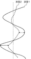
- the wavefronts of light having three wavelengths 1 to 3 included in the plane wave transmitted through the scattering plate are converted into different shapes by the scattering plate.
- the light whose wavefront is converted for each wavelength is reflected by a mirror having a mirror surface shaped so as to eliminate the difference in the optical path length at each location of the wavefront with respect to a specific wavelength, for example.
- the wavefront returns to a plane wave.
- FIG. 3A shows an example in which light of wavelength 2 returns to a plane wave among the light of three wavelengths 1 to 3.
- the wavefront shape for each wavelength is measured using, for example, a wavefront shape sensor.
- a mirror having a shape that eliminates the difference in optical path length at each position of the wavefront can be obtained by appropriately controlling a spatial light modulator (SLM) such as a variable shape mirror. That is, by controlling the mirror surface of the spatial light modulator according to the shape of the wavefront of the specific wavelength measured by the wavefront shape sensor, the light of the specific wavelength is returned to the plane wave. Further, when converted into wavefronts having different shapes for respective wavelengths, the wavefronts of light of other wavelengths have shapes different from those of plane waves.
- SLM spatial light modulator
- light having a wavefront of a specific wavelength described above passes through the optical system including the pinhole through the plane wave, so that the light of the wavefront other than the plane wave is scattered by the pinhole. That is, it is possible to form an image on a wavefront of a specific wavelength that has become a plane wave on the image sensor.
- a monochromatic image relating to the specific wavelength can be obtained by forming an image of the wavefront of the specific wavelength that has become a plane wave on the imaging element.
- FIG. 3 (B) light other than light of wavelength 2 which is a plane wave among light of three different wavelengths of wavelengths 1 to 3 is scattered by an optical system including a pinhole. That is, in this example, an image relating to wavelength 2 is obtained.
- the above procedure makes it possible to obtain a monochromatic image relating to a specific wavelength. And it becomes possible to obtain the image regarding many wavelengths by repeating said procedure with respect to several desired wavelength.
- the deformable mirror operates at an operating frequency of, for example, several kHz (kilohertz). That is, in the above-described procedure, for example, by using a deformable mirror as a spatial light modulator, it is possible to obtain a plane wave of light having several thousand wavelengths per second, for example.
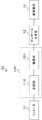
- FIG. 1 is a diagram illustrating a spectroscopic device according to the present embodiment.
- FIG. 2 is a diagram illustrating the imaging apparatus according to the present embodiment.
- the imaging device shown in FIG. 2 includes the spectroscopic device shown in FIG.
- the spectroscopic device 100 includes a modulation unit 110 and a demodulation unit 120.
- the modulator 110 converts the wavefront shape of light according to the wavelength.
- the demodulator 120 changes the phase of light having a specific wavelength selected from the light whose wavefront shape has been converted by the modulator 110 so as to be in a predetermined state.
- the demodulator 120 changes the phase of the light so that the light of which the wavefront shape has been converted by the modulator 110 is aligned with the light of a specific wavelength selected to become a plane wave.
- the imaging device 10 includes a collimator 11, the spectroscopic device 100 described above, a pinhole optical system 12, and an imaging element 13.
- the collimator 11 converts light related to a two-dimensional image of the object or the like into parallel light.
- the spectroscopic device 100 changes the phase of the selected light having a specific wavelength so as to be in a predetermined state such as parallel light, and emits the light.
- the pinhole optical system 12 forms an image on the imaging element 13 with the light converted into a plane wave by the spectroscopic device 100.
- the pinhole optical system 12 includes a pinhole.
- the image sensor 13 captures an image of light having a specific wavelength that is parallel light.
- the wavelength band of light targeted by the spectroscopic device 100 or the imaging device 10 is not limited.
- the spectroscopic device 100 or the imaging device 10 may target the wavelength band of visible light, or may target the wavelength band of infrared light or ultraviolet light.
- the image (wavefront) is decomposed into a plurality of two-dimensional pixels, for example, according to the pixels of the imaging element 13 or the like. That is, the modulation unit 110 converts the wavefront in units of, for example, a plurality of two-dimensional pixels according to the pixels of the image sensor 13 or the like.
- FIG. 4 shows an example of a specific configuration of the spectroscopic device 100 and the imaging device 10 having the spectroscopic device 100 in the present embodiment.
- the imaging device 10 according to the present embodiment includes a collimator 11, the spectroscopic device 100 described above, a pinhole optical system 12, and an imaging element 13.
- the scattering plate 111 is used as the modulation unit 110 of the spectroscopic device 100
- the variable shape mirror 121 is used as the demodulation unit 120.
- a block 16 that blocks the return light is provided as appropriate in order to avoid interference with the deformable mirror 121.
- the collimator 11 converts the light related to the two-dimensional image related to the object into parallel light.
- known means such as a collimator lens is used.
- a two-dimensional image incident on the collimator 11 is obtained by a lens 15 or the like as shown in FIG. In the example shown in FIG. 4, a lens 15 corresponding to the type of object is used as appropriate.
- the pinhole optical system 12 includes at least a pinhole.
- the pinhole optical system 12 forms an image of parallel light out of the light emitted from the spectroscopic device 100. That is, the pinhole optical system 12 scatters light that is not parallel light. In other words, the pinhole optical system 12 selectively transmits light having a wavelength that has been converted into parallel light by the spectroscopic device 100.
- the imaging element 13 images light having a wavelength that has been converted into parallel light by the spectroscopic device 100.
- a general image sensor such as a CMOS (Complementary Metal Oxide Semiconductor) image sensor or a CCD (Charge Coupled Device) is used as the image sensor 13.
- CMOS Complementary Metal Oxide Semiconductor
- CCD Charge Coupled Device
- the scattering plate 111 corresponding to the modulation unit 110 converts the wavefront shape according to the wavelength by utilizing the chromatic dispersion of the substance (that is, the difference in refractive index according to the wavelength of light). That is, the scattering plate 111 has a configuration in which the optical path length corresponding to the wavelength is different at least in part.
- the optical path length is represented by the product of the distance traveled by light when traveling through a medium and the refractive index of the medium.
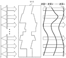
- FIG. 5 shows an example in which the scattering plate 111 converts the wavefront shape.
- FIG. 5 shows a cross section of the scattering plate 111. That is, in the example of FIG. 5, it is assumed that the scattering plate 111 extends from the front to the back of the drawing.
- FIG. 5 shows an example in which parallel light is incident on the scattering plate 111 for each predetermined pixel via a microlens array such as an array of GRIN (Gradient Index) lenses. That is, in the example shown in FIG. 5, the light is reduced in diameter by the microlens array (squeezed sufficiently small with respect to the size of the pixel in the surface direction) to the left surface of the scattering plate 111 in FIG. Incident for each pixel.
- GRIN Gradient Index
- the light incident on the scattering plate 111 is converted by the scattering plate 111 so as to have different wavefront shapes for each of the wavefronts 1 through n (n is a natural number). That is, the scattering plate 111 converts the wavefront shape of light that is parallel light into a distorted wavefront that differs depending on the wavelength of the light.
- the light whose wavefront shape has been converted is emitted from the right surface of the scattering plate 111 in FIG.
- the shape of the contour of the surface on which the light of the scattering plate 111 enters or exits is appropriately determined according to the light incident on the scattering plate 111 or the like.
- the surface of the scattering plate 111 on which light enters or exits is, for example, rectangular.
- the deformable mirror 121 corresponding to the demodulator 120 is a mirror that can change the shape of the mirror surface.
- the variable shape mirror 121 changes the phase of the light of the selected wavelength among the light whose wavefront shape has been converted by the scattering plate 111 by changing the shape of the mirror surface. That is, the deformable mirror 121 has a mirror surface having a shape corresponding to the wavefront shape of the light. In this case, the deformable mirror 121 changes the phase so that the light of the selected wavelength becomes parallel light. . In this case, light of other wavelengths has a wavefront different from that of parallel light.
- variable shape mirror 121 makes it possible to change the phase so that a plurality of light beams having different wavelengths become parallel light by changing the shape of the mirror surface according to the wavefront shape for each wavelength.
- the shape of the mirror surface of the deformable mirror 121 is sequentially changed so that each of the light of a plurality of wavelengths becomes parallel light. Change the phase.
- the scattering plate 111 serving as the modulation unit 110 converts the wavefront shape of the parallel light related to the incident two-dimensional image according to the wavelength.
- the scattering plate 111 converts each wavefront shape of the plurality of wavelength lights to such an extent that the wavefront shapes can be distinguished by the variable shape mirror 121.
- the magnitude of the difference between any two wavefront shapes of a plurality of wavelength lights (that is, the difference in optical path length in at least one pixel) is It needs to be larger than the resolution. That is, when the difference in wavefront shape with respect to two wavelength lights indicated by the arrows in FIG. 6 is larger than the resolution of the shape variable mirror 121 in one or more pixels, the shape variable mirror 121 It becomes possible to change the phase individually.
- the deformable mirror 121 causes the light having the wavelength to be a plane wave. Cannot change the mirror surface. That is, in this case, it is difficult for the shape variable mirror 121 to change the phase of the wavefront so that the light of the wavelength becomes a plane wave. Therefore, when the wavefront shape is converted by the scattering plate 111, the difference in the optical path length for each pixel needs to be included in the movable range of the variable shape mirror 121 for each wavefront of light having a target wavelength. .
- An example of the relationship between the wavefront shape conversion by the scattering plate 111 and the number of wavelengths that can be distinguished by the variable shape mirror 121 is as follows. In this example, it is assumed that the resolution of the deformable mirror with respect to the incident direction of light is 1 nm (nanometer). In this case, if there is a difference of 1 nm or more in the optical path lengths of the wavefront shapes of the two wavelength lights, the wavefronts of the two wavelength lights are distinguished.
- the scattering plate 111 is quartz glass having a thickness of 1 mm (millimeter) and a wavelength from 340 nm to 900 nm is a measurement target.
- the difference in refractive index for light in the wavelength band is approximately 0.02692 based on the refractive index for light of 340 nm and the refractive index for light of 900 nm.
- the difference in optical path length for light in the wavelength band is obtained as 2.692 * 10 ⁇ 5 m (meters) by multiplying the difference in refractive index by the thickness of the scattering plate 111. “*” Means multiplication.
- the number of wavelengths (hereinafter sometimes referred to as “bands”) that can be distinguished by the deformable mirror 121 is the difference in optical path length. Is divided by the resolution of the deformable mirror 121 to obtain 26920 bands.
- the material used for the scattering plate 111 is not particularly limited.
- the scattering plate 111 is preferably formed of a material having high light transmittance and large chromatic dispersion, for example.
- the scattering plate 111 is formed of a material having a large chromatic dispersion, the difference in optical path length according to the wavelength is increased. That is, the difference in wavefront shape for each wavelength increases. And it becomes possible to distinguish light of a larger number of wavelengths.
- a material having a large chromatic dispersion generally varies depending on the wavelength.
- quartz glass is used.
- the near-infrared or mid-infrared is primarily intended, for example CaF 2 is (calcium fluoride) is used.
- ZnSe zinc selenide is used when medium infrared rays or far infrared rays are mainly targeted.
- the configuration of the scattering plate 111 are conceivable so that light of many wavelengths is converted into different wavefront shapes.
- the scattering plate 111 converts the light of multiple wavelengths into different wavefront shapes, so that the phase of the light of multiple wavelengths is aligned by the demodulator 120. That is, the scattering plate 111 converts light having a large number of wavelengths into different wavefront shapes, so that images having a large number of wavelengths can be acquired.
- the thickness of the surface of the scattering plate 111 may be changed depending on the part. That is, unevenness may be formed on the surface of the scattering plate 111.
- the thickness of the surface of the scattering plate 111 can be changed according to the portion of the surface of the scattering plate 111 such as for each pixel.
- the difference in optical path length for each wavelength changes. For example, when the thickness of the scattering plate 111 increases, the difference in optical path length for each wavelength increases in accordance with the thickness of the scattering plate 111. Therefore, when the thickness of the surface of the scattering plate 111 is changed depending on the part, the difference in the optical path length for each wavelength corresponding to the part of the scattering plate 111 increases.
- the scattering plate 111 may be formed by combining a plurality of layers of the same or different materials.
- the scattering plate 111 may be formed, for example, by bonding a plurality of layers of the same or different materials, or by providing a plurality of layers of the same or different materials at intervals. It may be formed.
- each of the plurality of layers is preferably made of a material having different color dispersion properties, for example.
- the difference in the optical path difference for each wavelength becomes larger than when the scattering plate 111 is formed of one material.
- the difference in wavefront shape for each wavelength increases. Therefore, it is possible to acquire images with more wavelengths.
- the thickness of the scattering plate 111 may be changed depending on the surface portion.
- the thickness of each layer forming the scattering plate 111 may be changed according to the surface portion.
- the scattering plate 111 may have a configuration in which the traveling direction of light is changed at least in part according to the wavelength. More specifically, the surface of the scattering plate 111 and the surface of each layer forming the scattering plate 111 are directed in a direction different from the direction perpendicular to the traveling direction of the parallel light incident on the scattering plate 111 depending on the part.
- the shape may extend.
- the surface of the scattering plate 111 may have a shape different from the planar shape.
- at least one of the surfaces of the scattering plate 111 may have a shape extending in a direction oblique to the traveling direction of parallel light incident on the scattering plate 111.
- the direction of the surface of the scattering plate 111 may be different for each part of the surface.
- the surface of the scattering plate 111 includes each surface of a plurality of layers forming the scattering plate 111.
- the traveling direction of the light passing through the scattering plate 111 (that is, the vector of the light beam) Orientation) can be changed. Further, the extending direction of the surface of the scattering plate 111 is changed in each of the surfaces of the scattering plate 111, whereby the traveling direction of light passing through each part of the surface of the scattering plate 111 is changed. For example, the traveling direction of the light passing through the scattering plate 111 is changed for each pixel on the surface of the scattering plate 111. Moreover, the change in the traveling direction of light varies depending on the wavelength.
- the traveling direction of light in each part of the wavefront changes for each wavelength. That is, the surface of the scattering plate 111 extends in an oblique direction with respect to the incident direction, so that the surface of the scattering plate 111 extends only in the direction perpendicular to the incident direction.
- a large difference is given to the wavefront shape for each wavelength.
- the number of wavelengths whose phases are adjusted by the variable shape mirror 121 can be increased.
- the roughness of the surface may be changed according to the site.
- the surface of the scattering plate 111 may have a different direction in which the surface extends depending on the part, or may have a different thickness depending on the part.
- the direction in which the surface extends may be different depending on the portion of the surface. In this case, each thickness may differ depending on the surface portion.
- FIG. 7A to 7C each show a cross-sectional view of a specific configuration example of the scattering plate 111.
- FIG. FIG. 7A shows an example in which the scattering plate 111 is formed of one material of the material 1.
- FIG. 7B shows an example in which the scattering plate 111 is formed of layers of two different materials, materials 1 and 2.
- FIG. 7C shows an example in which the scattering plate 111 is formed of layers of three different materials 1 to 3.
- parallel light is incident from the left side of each scattering plate 111 so as to be perpendicular to the left side surface of the scattering plate 111.
- the shape of one surface of the scattering plate 111 is different from the planar shape. That is, in the example of FIG. 7A, the shape of a part of one surface of the scattering plate 111 is formed so as to be inclined with respect to the traveling direction of the parallel light. In the example of FIG. 7A, the thickness of a part of one surface of the scattering plate 111 is different from the other parts. As an example, in the example of FIG. 7A, the lower part of the scattering plate 111 in the drawing has a larger thickness than other parts.
- the shape of the surface of the scattering plate 111 that is in contact with the layers of different materials is different from the planar shape as in the example of FIG. Yes.
- the materials 1 to 3 are not particularly limited.
- materials having different color dispersion are used.
- a material having different chromatic dispersion is used for the scattering plate, so that the difference in wavefront shape for each wavelength can be increased.
- each scattering plate 111 may have the various structures described above with respect to the depth direction in the drawing.
- the wavefront shape is converted by the scattering plate 111 so that the light of one pixel enters another pixel, there is a possibility that crosstalk occurs between the pixels. In order to avoid this, it is necessary to determine the traveling direction of the light of each pixel so that the light of each pixel does not enter the other pixels.
- FIG. 8 is a diagram relating to conditions of the light traveling direction in each pixel.
- the demodulator 120 is the deformable mirror 121
- the width of one pixel on the scattering plate 111 is c
- the distance from the surface of the scattering plate 111 on the deformable mirror 121 side to the mirror surface of the deformable mirror 121 is Assume that s.
- it is assumed that light incident on each pixel is reduced in diameter by, for example, a microlens array using a GRIN lens.
- the deformable mirror 121 that is the demodulator 120 is a mirror that can change the shape of the mirror surface by MEMS (Micro Electro Mechanical Systems) or an electromagnetic method. By changing the shape of the mirror surface, the deformable mirror 121 changes the phase of the wavefront.
- MEMS Micro Electro Mechanical Systems
- variable shape mirror is used as the variable shape mirror 121.
- the deformable mirror 121 is, for example, a deformable mirror whose surface shape is changed by a MEMS actuator.
- the mirror surface has a square shape with a side of 4 mm, and the number of actuators is 144.
- the distance between the actuators is 0.33 mm, and the resolution (shortest operating distance) is 1 nm.
- the operating frequency of the actuator is 8 kHz at maximum.
- the shape of the mirror surface is determined based on the operating distance of the actuator (that is, the movement distance of the actuator in the direction perpendicular to the mirror surface when the mirror surface is planar) and the distance between the actuators.
- the demodulator 120 is the variable shape mirror 121
- the number of wavelengths that can be dispersed per unit time is determined according to the operating frequency of the variable shape mirror 121.
- the operating frequency of the deformable mirror 121 is 8 kHz
- processing of 8000 bands can be performed in one second.
- the spectrum is performed in about 0.03 seconds. That is, in the spectroscopic device 100 according to the present embodiment, for example, the deformable mirror 121 is used as the demodulator 120, so that high-speed spectroscopy according to the operating frequency of the deformable mirror 121 is possible.
- the demodulator 120 may be realized by a different type of spatial light modulator from the deformable mirror 121.
- a spatial light modulator using liquid crystal is used as the demodulator 120.
- the phase is delayed according to the wavelength by controlling the liquid crystal.
- the phases of the light of the specific wavelength are aligned.
- the demodulation unit 120 may be realized using a technique based on the phase shift interferometry.
- a transfer function related to phase conversion by the scattering plate 111 is obtained based on a change in phase for each wavelength by the scattering plate 111 obtained in advance. And based on this transfer function, the light which wavefront shape was converted for every wavelength with the scattering plate 111 is imaged, and the process which changes the phase of the selected specific wavelength light with respect to the imaged image is performed. Is called.
- a series of processing is realized by an information processing apparatus such as a PC (Personal Computer).
- the demodulator 120 only needs to be able to change the phase so that light of the selected wavelength becomes a plane wave out of the light whose wavefront shape is converted according to the wavelength by the modulator 110.
- the demodulator 120 may be realized by a mechanism different from the deformable mirror 121.
- the mechanism used as the demodulator 120 may be appropriately determined according to the required operation speed and other conditions.
- the demodulator 120 is preferably a mechanism that can handle a large number of bands at high speed, such as the deformable mirror 121.
- Adjustment procedure of demodulator 120 In the spectroscopic device 100 according to the present embodiment, in order to align the phases of light of specific wavelengths, for example, when the deformable mirror 121 is used as the demodulator 120, the shape of the mirror surface of the deformable mirror 121 corresponding to the wavelength is determined. There is a need. When determining the shape of the mirror surface of the deformable mirror 121, it is necessary to grasp the wavefront shape for each wavelength. The wavefront shape converted by the scattering plate 111 that is the modulation unit 110 is obtained by the following procedure for each wavelength.
- FIG. 9 shows an example of a configuration used when adjusting the demodulation unit 120.
- monochromatic light having a specific wavelength, which is parallel light enters the scattering plate 111.
- the monochromatic light is obtained, for example, when white light is incident on the spectrophotometer 17 through the lens 15-1 or the like. Then, the monochromatic light thus obtained is incident on the collimator 11 through the lens 15-2 or the like, so that monochromatic light that is parallel light is obtained.
- the monochromatic light is converted into a wavefront shape corresponding to the wavelength by the scattering plate 111.
- the monochromatic light whose wavefront shape has been converted is introduced into the wavefront shape sensor 18.
- monochromatic light is introduced into the wavefront shape sensor 18 via the variable shape mirror 121.
- the deformable mirror 121 is controlled to be a flat surface.
- the monochromatic light whose wavefront shape has been converted may be directly introduced into the wavefront shape sensor 18 without passing through the variable shape mirror 121.
- the wavefront shape sensor 18 obtains the wavefront shape of the monochromatic light converted by the scattering plate 111.
- the shape of the mirror surface of the variable shape mirror 121 is obtained based on the obtained wavefront shape so that the light of the wavelength of the monochromatic light is a plane wave.
- the shape of the mirror surface of the deformable mirror 121 is obtained using a known method.
- the above-described operation is performed on monochromatic light of other wavelengths, so that the shape of the mirror surface of the deformable mirror 121 is obtained so that the monochromatic light of other wavelengths is a plane wave.
- Monochromatic light of other wavelengths is obtained by changing the diffraction wavelength of the spectrophotometer 17 or the like.
- the shape of the mirror surface of the deformable mirror 121 can be determined for a plurality of desired wavelengths by repeatedly performing the above-described operation for a plurality of wavelengths.
- the shape of the mirror surface of the variable shape mirror 121 is obtained for each of the scattering plates 111.
- the demodulator 120 changes the phase of light of a specific wavelength, information on the wavefront shape obtained as described above is appropriately used. Used.
- the demodulator 120 parallelizes the phase of light having a specific wavelength among the light whose wavefront shape is converted for each wavelength by the modulator 110 such as the scattering plate 111. It changes so that it may become predetermined
- the demodulator 120 uses a variable shape mirror 121 or the like.
- the deformable mirror 121 can operate at an operating frequency of several kHz. That is, by using the deformable mirror 121 in the demodulator 120, the spectroscopic device 100 can obtain, for example, plane waves of several thousand bands of light per second.
- the known hyperspectral imaging technique may require operations such as exchanging a filter for selecting a specific wavelength and scanning light dispersed by a diffraction grating during spectroscopy. If these operations are required when acquiring an image for each wavelength, it may take several seconds to acquire an image of one wavelength. In addition, a mechanism for these operations may be required.
- the spectroscopic device 100 according to the present embodiment enables high-speed spectroscopy. Moreover, the imaging device 10 having the spectroscopic device 100 according to the present embodiment can obtain images for a large number of wavelengths for hyperspectral imaging at high speed.
- spectroscopic device 100 Application example of spectroscopic device and imaging device
- the above-described spectroscopic device 100 and the imaging device 10 including the spectroscopic device 100 are applied to various fields.
- the imaging device 10 is used in the same manner as an existing device for hyperspectral imaging.
- the imaging device 10 is mounted on, for example, a satellite or an aircraft, and is used for environmental investigations.
- the imaging device 10 can obtain images for a number of wavelengths for hyperspectral imaging at high speed. For this reason, the imaging apparatus 10 is used for applications that require high-speed image acquisition.
- the imaging device 10 for security of an important facility or the like, it is possible to quickly identify a target object and to plan a quick countermeasure based on the identified information.
- the imaging device 10 is used for investigations of fires of chemical plants, pollutant emissions from factories, etc., so that the location of fires can be identified and the diffusion status of toxic substances can be observed and predicted. It becomes possible.
- the use of the imaging device 10 in fields such as life science and food science facilitates detailed analysis of chemical reactions and the like occurring inside cells and microorganisms.
- the imaging measure 10 facilitates analysis of the time course of these chemical reactions.
- the imaging device 10 when used as an endoscope or the like, it is possible to detect a disease or a resection site and to diagnose a state in a living body at high speed. This makes it possible to reduce the patient's pain.
- the imaging device 10 capable of detecting infrared rays is mounted on an automobile or the like, it is possible to recognize a person around the vehicle based on the radiation wavelength characteristics of the human body.
- the degree of freedom in operation is increased by obtaining images at high speed.
- the spectroscopic device 100 is used as a general spectroscopic device. Even in this case, the processing efficiency can be improved by performing high-speed spectroscopy.
- Appendix 1 Modulation means for converting the wavefront shape of light according to the wavelength;
- a spectroscopic device comprising demodulating means for changing the phase of light having a selected wavelength out of the light whose wavefront shape has been converted so as to be in a predetermined state.
- Appendix 2 The spectroscopic device according to appendix 1, wherein the demodulation unit changes the phase of the light having the selected wavelength so as to be parallel light.
- Appendix 3) The spectroscopic device according to appendix 1 or 2, wherein the modulation unit is a scattering plate having at least a part of an optical path length for each wavelength.
- Appendix 14 A collimator that makes the light related to the two-dimensional image the first parallel light;
- the spectroscopic device according to any one of appendices 1 to 13, wherein the phase of light having a specific wavelength among the first parallel light is changed to be parallel light;
- a pinhole optical system that forms an image of the second parallel light emitted from the spectroscopic device;
- An imaging apparatus comprising: an image sensor that images the second parallel light.
Landscapes
- Physics & Mathematics (AREA)
- Spectroscopy & Molecular Physics (AREA)
- General Physics & Mathematics (AREA)
- Spectrometry And Color Measurement (AREA)
- Mechanical Light Control Or Optical Switches (AREA)
- Studio Devices (AREA)
Abstract
Le problème décrit par la présente invention est de fournir un dispositif spectroscopique et similaire(s) permettant d'atteindre un spectre à grande vitesse. La solution selon l'invention porte sur un dispositif spectroscopique comportant : un moyen de modulation, pour convertir une forme de front d'onde de la lumière selon une longueur d'onde ; et un moyen de démodulation, pour changer une phase de la lumière d'une longueur d'onde sélectionnée dans un état prédéterminé, parmi les lumières dont les formes de front d'onde ont été modulées.
Priority Applications (2)
| Application Number | Priority Date | Filing Date | Title |
|---|---|---|---|
| JP2018544725A JPWO2018070206A1 (ja) | 2016-10-12 | 2017-09-21 | 分光装置及び撮像装置 |
| US16/341,133 US10908021B2 (en) | 2016-10-12 | 2017-09-21 | Spectroscopic device and imaging device |
Applications Claiming Priority (2)
| Application Number | Priority Date | Filing Date | Title |
|---|---|---|---|
| JP2016-201022 | 2016-10-12 | ||
| JP2016201022 | 2016-10-12 |
Publications (1)
| Publication Number | Publication Date |
|---|---|
| WO2018070206A1 true WO2018070206A1 (fr) | 2018-04-19 |
Family
ID=61905325
Family Applications (1)
| Application Number | Title | Priority Date | Filing Date |
|---|---|---|---|
| PCT/JP2017/034067 Ceased WO2018070206A1 (fr) | 2016-10-12 | 2017-09-21 | Dispositif spectroscopique et dispositif d'imagerie |
Country Status (3)
| Country | Link |
|---|---|
| US (1) | US10908021B2 (fr) |
| JP (1) | JPWO2018070206A1 (fr) |
| WO (1) | WO2018070206A1 (fr) |
Families Citing this family (3)
| Publication number | Priority date | Publication date | Assignee | Title |
|---|---|---|---|---|
| CN114594587B (zh) * | 2020-12-07 | 2023-06-09 | 中国科学院长春光学精密机械与物理研究所 | 一种紫外巡天的光学成像系统 |
| JP7730686B2 (ja) * | 2021-08-11 | 2025-08-28 | 株式会社ディスコ | 光照射装置 |
| CN115979422B (zh) * | 2023-02-15 | 2026-03-31 | 中国科学院国家天文台南京天文光学技术研究所 | 一种缺陷散射计算重构光谱探测装置及方法 |
Citations (10)
| Publication number | Priority date | Publication date | Assignee | Title |
|---|---|---|---|---|
| JP2001036471A (ja) * | 1999-07-15 | 2001-02-09 | Mitsubishi Electric Corp | 波面誤差検出装置及び波面誤差検出方法 |
| JP2002525596A (ja) * | 1998-09-23 | 2002-08-13 | アイシス イノヴェイション リミテッド | 波面感知装置 |
| JP2002544553A (ja) * | 1999-05-18 | 2002-12-24 | キャンパス テクノロジーズ アーゲー | 光信号検出または生成装置 |
| US20030053052A1 (en) * | 2001-09-19 | 2003-03-20 | Braun David M. | Optical monochromators having time dispersion correction |
| JP2005512075A (ja) * | 2001-12-10 | 2005-04-28 | ザイゴ コーポレーション | 位相シフト干渉分析の方法及びシステム |
| JP2009526984A (ja) * | 2006-02-16 | 2009-07-23 | オーエヌウエールア(オフィス ナショナル デチュード エ ドゥ ルシェルシュ アエロスパシアル) | 周波数差マルチラテラル干渉法を通じて波面を解析する方法 |
| JP2011053150A (ja) * | 2009-09-03 | 2011-03-17 | Nikon Corp | 波面測定方法及び波面測定装置 |
| CN102818631A (zh) * | 2012-07-30 | 2012-12-12 | 中国科学院上海光学精密机械研究所 | 基于随机波前相位调制的压缩光谱成像系统 |
| WO2016056147A1 (fr) * | 2014-10-08 | 2016-04-14 | オリンパス株式会社 | Système optique de formation d'image, dispositif d'éclairage, et dispositif d'observation |
| JP2016168192A (ja) * | 2015-03-12 | 2016-09-23 | キヤノン株式会社 | 画像撮像装置及びその制御方法 |
Family Cites Families (3)
| Publication number | Priority date | Publication date | Assignee | Title |
|---|---|---|---|---|
| US6735012B2 (en) * | 2002-03-22 | 2004-05-11 | The Boeing Company | System for phase modulating an incoming optical wavefront |
| JP2015055819A (ja) | 2013-09-13 | 2015-03-23 | 株式会社トプコン | 走査型投影表示光学系、および走査型投影表示装置 |
| JPWO2016052743A1 (ja) * | 2014-10-03 | 2017-07-27 | オリンパス株式会社 | 光軸方向走査型顕微鏡装置 |
-
2017
- 2017-09-21 JP JP2018544725A patent/JPWO2018070206A1/ja active Pending
- 2017-09-21 US US16/341,133 patent/US10908021B2/en active Active
- 2017-09-21 WO PCT/JP2017/034067 patent/WO2018070206A1/fr not_active Ceased
Patent Citations (10)
| Publication number | Priority date | Publication date | Assignee | Title |
|---|---|---|---|---|
| JP2002525596A (ja) * | 1998-09-23 | 2002-08-13 | アイシス イノヴェイション リミテッド | 波面感知装置 |
| JP2002544553A (ja) * | 1999-05-18 | 2002-12-24 | キャンパス テクノロジーズ アーゲー | 光信号検出または生成装置 |
| JP2001036471A (ja) * | 1999-07-15 | 2001-02-09 | Mitsubishi Electric Corp | 波面誤差検出装置及び波面誤差検出方法 |
| US20030053052A1 (en) * | 2001-09-19 | 2003-03-20 | Braun David M. | Optical monochromators having time dispersion correction |
| JP2005512075A (ja) * | 2001-12-10 | 2005-04-28 | ザイゴ コーポレーション | 位相シフト干渉分析の方法及びシステム |
| JP2009526984A (ja) * | 2006-02-16 | 2009-07-23 | オーエヌウエールア(オフィス ナショナル デチュード エ ドゥ ルシェルシュ アエロスパシアル) | 周波数差マルチラテラル干渉法を通じて波面を解析する方法 |
| JP2011053150A (ja) * | 2009-09-03 | 2011-03-17 | Nikon Corp | 波面測定方法及び波面測定装置 |
| CN102818631A (zh) * | 2012-07-30 | 2012-12-12 | 中国科学院上海光学精密机械研究所 | 基于随机波前相位调制的压缩光谱成像系统 |
| WO2016056147A1 (fr) * | 2014-10-08 | 2016-04-14 | オリンパス株式会社 | Système optique de formation d'image, dispositif d'éclairage, et dispositif d'observation |
| JP2016168192A (ja) * | 2015-03-12 | 2016-09-23 | キヤノン株式会社 | 画像撮像装置及びその制御方法 |
Also Published As
| Publication number | Publication date |
|---|---|
| US20190242749A1 (en) | 2019-08-08 |
| JPWO2018070206A1 (ja) | 2019-08-29 |
| US10908021B2 (en) | 2021-02-02 |
Similar Documents
| Publication | Publication Date | Title |
|---|---|---|
| US12174070B2 (en) | Fabry-perot fourier transform spectrometer | |
| US11002601B2 (en) | Spectroscopic microscope and spectroscopic observation method | |
| JP5635624B2 (ja) | 小型干渉分光計 | |
| CN100437020C (zh) | 多波长成像光谱仪的方法和装置 | |
| US9716846B2 (en) | Full-frame, programmable hyperspectral imager | |
| US20190277698A1 (en) | Microelectromechanical system (mems) and (mem) optical interferometer for hyper-spectral imaging and analysis | |
| JP5563405B2 (ja) | 分光画像取得装置及び方法 | |
| CN107192349B (zh) | 光检测装置 | |
| Boniface et al. | Rapid broadband characterization of scattering medium using hyperspectral imaging | |
| WO2018070206A1 (fr) | Dispositif spectroscopique et dispositif d'imagerie | |
| US20050122529A1 (en) | Measurement system of three-dimensional shape of transparent thin film using acousto-optic tunable filter | |
| US10379275B2 (en) | Optical filter including plates for filtering light and optical measuring device employing optical filter | |
| JP5371362B2 (ja) | レーザ顕微鏡装置 | |
| CN114341602B (zh) | 分光测定装置 | |
| US20220229213A1 (en) | Diffraction element and imaging device | |
| AU2015261653B2 (en) | Fabry-Perot Fourier transform spectrometer | |
| JP2008008842A (ja) | 電磁波測定装置 | |
| JP2025533335A (ja) | 媒質の1つまたは複数の光学パラメータの測定のためのアセンブリおよびアセンブリを使用する方法 | |
| RU2673784C1 (ru) | Двухкомпонентный интерферометр общего пути | |
| WO2023176638A1 (fr) | Dispositif optique |
Legal Events
| Date | Code | Title | Description |
|---|---|---|---|
| 121 | Ep: the epo has been informed by wipo that ep was designated in this application |
Ref document number: 17859922 Country of ref document: EP Kind code of ref document: A1 |
|
| ENP | Entry into the national phase |
Ref document number: 2018544725 Country of ref document: JP Kind code of ref document: A |
|
| NENP | Non-entry into the national phase |
Ref country code: DE |
|
| 122 | Ep: pct application non-entry in european phase |
Ref document number: 17859922 Country of ref document: EP Kind code of ref document: A1 |