WO2018078747A1 - Dispositif de transfert et procédé de transfert de trame - Google Patents
Dispositif de transfert et procédé de transfert de trame Download PDFInfo
- Publication number
- WO2018078747A1 WO2018078747A1 PCT/JP2016/081756 JP2016081756W WO2018078747A1 WO 2018078747 A1 WO2018078747 A1 WO 2018078747A1 JP 2016081756 W JP2016081756 W JP 2016081756W WO 2018078747 A1 WO2018078747 A1 WO 2018078747A1
- Authority
- WO
- WIPO (PCT)
- Prior art keywords
- frame
- code
- unit
- transfer
- fcs
- Prior art date
- Legal status (The legal status is an assumption and is not a legal conclusion. Google has not performed a legal analysis and makes no representation as to the accuracy of the status listed.)
- Ceased
Links
Images





Classifications
-
- H—ELECTRICITY
- H04—ELECTRIC COMMUNICATION TECHNIQUE
- H04L—TRANSMISSION OF DIGITAL INFORMATION, e.g. TELEGRAPHIC COMMUNICATION
- H04L1/00—Arrangements for detecting or preventing errors in the information received
- H04L1/004—Arrangements for detecting or preventing errors in the information received by using forward error control
- H04L1/0045—Arrangements at the receiver end
-
- H—ELECTRICITY
- H04—ELECTRIC COMMUNICATION TECHNIQUE
- H04L—TRANSMISSION OF DIGITAL INFORMATION, e.g. TELEGRAPHIC COMMUNICATION
- H04L1/00—Arrangements for detecting or preventing errors in the information received
- H04L1/20—Arrangements for detecting or preventing errors in the information received using signal quality detector
- H04L1/201—Frame classification, e.g. bad, good or erased
-
- H—ELECTRICITY
- H04—ELECTRIC COMMUNICATION TECHNIQUE
- H04L—TRANSMISSION OF DIGITAL INFORMATION, e.g. TELEGRAPHIC COMMUNICATION
- H04L43/00—Arrangements for monitoring or testing data switching networks
- H04L43/08—Monitoring or testing based on specific metrics, e.g. QoS, energy consumption or environmental parameters
- H04L43/0823—Errors, e.g. transmission errors
-
- H—ELECTRICITY
- H04—ELECTRIC COMMUNICATION TECHNIQUE
- H04L—TRANSMISSION OF DIGITAL INFORMATION, e.g. TELEGRAPHIC COMMUNICATION
- H04L1/00—Arrangements for detecting or preventing errors in the information received
- H04L1/004—Arrangements for detecting or preventing errors in the information received by using forward error control
- H04L1/0056—Systems characterized by the type of code used
- H04L1/0061—Error detection codes
-
- H—ELECTRICITY
- H04—ELECTRIC COMMUNICATION TECHNIQUE
- H04L—TRANSMISSION OF DIGITAL INFORMATION, e.g. TELEGRAPHIC COMMUNICATION
- H04L1/00—Arrangements for detecting or preventing errors in the information received
- H04L1/0078—Avoidance of errors by organising the transmitted data in a format specifically designed to deal with errors, e.g. location
- H04L1/0079—Formats for control data
-
- H—ELECTRICITY
- H04—ELECTRIC COMMUNICATION TECHNIQUE
- H04L—TRANSMISSION OF DIGITAL INFORMATION, e.g. TELEGRAPHIC COMMUNICATION
- H04L1/00—Arrangements for detecting or preventing errors in the information received
- H04L1/24—Testing correct operation
- H04L1/245—Testing correct operation by using the properties of transmission codes
-
- H—ELECTRICITY
- H04—ELECTRIC COMMUNICATION TECHNIQUE
- H04L—TRANSMISSION OF DIGITAL INFORMATION, e.g. TELEGRAPHIC COMMUNICATION
- H04L12/00—Data switching networks
- H04L12/28—Data switching networks characterised by path configuration, e.g. LAN [Local Area Networks] or WAN [Wide Area Networks]
-
- H—ELECTRICITY
- H04—ELECTRIC COMMUNICATION TECHNIQUE
- H04L—TRANSMISSION OF DIGITAL INFORMATION, e.g. TELEGRAPHIC COMMUNICATION
- H04L41/00—Arrangements for maintenance, administration or management of data switching networks, e.g. of packet switching networks
- H04L41/06—Management of faults, events, alarms or notifications
- H04L41/0677—Localisation of faults
-
- H—ELECTRICITY
- H04—ELECTRIC COMMUNICATION TECHNIQUE
- H04L—TRANSMISSION OF DIGITAL INFORMATION, e.g. TELEGRAPHIC COMMUNICATION
- H04L43/00—Arrangements for monitoring or testing data switching networks
- H04L43/08—Monitoring or testing based on specific metrics, e.g. QoS, energy consumption or environmental parameters
- H04L43/0805—Monitoring or testing based on specific metrics, e.g. QoS, energy consumption or environmental parameters by checking availability
- H04L43/0811—Monitoring or testing based on specific metrics, e.g. QoS, energy consumption or environmental parameters by checking availability by checking connectivity
-
- H—ELECTRICITY
- H04—ELECTRIC COMMUNICATION TECHNIQUE
- H04L—TRANSMISSION OF DIGITAL INFORMATION, e.g. TELEGRAPHIC COMMUNICATION
- H04L49/00—Packet switching elements
- H04L49/25—Routing or path finding in a switch fabric
- H04L49/252—Store and forward routing
Definitions
- the present invention relates to a transfer device and a frame transfer method for transferring a frame.
- Ethernet registered trademark
- Ethernet is already popular for consumer use, and the equipment is inexpensive and capable of high-speed communication.
- Ethernet has not been a standard that can meet the strict requirements of industrial applications such as high reliability and low latency.
- Non-patent Document 1 In the IEEE (Institute of Electrical and Electronics Engineers) 802.3br IET (Interspersing Express Traffic) task force, standardization activities for the IET method, which is a low-delay transfer method that can use bandwidth effectively, are performed (Non-patent Document 1).
- the transfer device minimizes the delay time by transferring an express frame, which is a frame with a severe delay requirement, by a cut-through method.
- an express frame transfer request is generated during transfer of a normal frame, which is a frame with a strict request for delay
- the transfer device interrupts and divides the transfer of the normal frame, interrupts and transfers the express frame, and transfers the express frame. After completion of, transfer of the remaining normal frames divided is resumed. The divided normal frames are combined and restored by the link-by-link counterpart device.
- a packet transfer device that transfers a frame by a cut-through method stores an inverted version of the CRC (Cyclic Redundancy Check) calculation result of the frame data in a DCS (Data Check Sequence) field uniquely defined in the frame.
- CRC Cyclic Redundancy Check
- DCS Data Check Sequence
- the DCS field is a unique field
- the DCS field is inserted into the data area of the frame in the Ethernet standard. For this reason, the DCS field is increased to the original data length, and there is a problem that frame transfer is delayed by the increase of the DCS field.
- the present invention has been made in view of the above, and in a network including a plurality of transfer devices, transfer that can identify a location where a failure occurs when an error is detected in a frame without delaying frame transfer
- the object is to obtain a device.
- the transfer apparatus of the present invention includes a calculation unit that calculates a first code that is a frame check sequence code of a received frame that is a received frame.
- the transfer apparatus compares the first code with the second code that is the frame check sequence code stored in the received frame, and indicates that the two codes that are compared match or do not match A first comparison unit that outputs a comparison result is provided.
- the transfer device compares the first code with the third code obtained by bit-inverting each bit of the second code, and the second comparison result indicating that the two codes thus compared match or do not match Is provided.
- the transfer apparatus includes an error determination unit that determines an error state of the received frame based on the first comparison result and the second comparison result.
- the transfer device updates the second code with the fourth code obtained by bit-inverting each bit of the first code when transferring the received frame to the subsequent device.
- the update part which performs is characterized by the above-mentioned.
- the transfer device has an effect that, in a network including a plurality of transfer devices, when an error is detected in a frame without delaying the transfer of the frame, it is possible to specify a location where a failure has occurred.
- FIG. 1 is a diagram illustrating a configuration example of a network including a transfer device according to a first embodiment; The figure which shows the example of the detection state of the error in each transfer device when the failure occurs in the network which includes the general transfer device
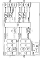
- FIG. 1 is a block diagram illustrating a configuration example of a transfer device according to a first embodiment; The figure which shows the example of the frame format of the frame transferred with the transfer apparatus concerning Embodiment 1 6 is a flowchart showing frame transfer processing of the transfer apparatus according to the first embodiment; The figure which shows the example of the detection state of the error in each transfer apparatus when a failure generate
- FIG. 3 is a diagram illustrating an example in which the processing circuit of the transfer device according to the first embodiment is configured by a CPU and a memory.
- FIG. 3 is a diagram illustrating an example when the processing circuit of the transfer apparatus according to the first embodiment is configured by dedicated hardware.
- FIG. 3 is a block diagram showing a configuration example of a transfer apparatus according to the second embodiment.
- 10 is a flowchart showing frame transfer processing of the transfer apparatus according to the second embodiment. The figure which shows the example of the frame transfer operation
- FIG. 1 is a diagram illustrating a configuration example of a network 5 including transfer apparatuses 1 to 4 according to the first embodiment of the present invention.
- the network 5 includes transfer devices 1 to 4.
- the transfer device 1 receives a frame from the left transfer device (not shown)
- the transfer device 1 outputs the frame to the transfer device 2 by the IET method, that is, transfers the frame.
- the transfer apparatuses 2 and 3 receive a frame from the left transfer apparatus
- the transfer apparatuses 2 and 3 output the frame to the right transfer apparatus.
- the transfer device 4 When receiving the frame from the left transfer device 3, the transfer device 4 outputs the frame to the right transfer device (not shown).
- transfer devices similar to the transfer devices 1 to 4 are also connected to the left side of the transfer device 1 and the right side of the transfer device 4.
- the transfer apparatuses 1 to 4 regardless of whether or not the transfer apparatuses 1 to 4 have an error in the frame due to a failure that occurred in the transmission stage before the previous transfer apparatus, the transfer apparatuses 1 to 4 use the transmission path immediately before the own transfer apparatus. Detect whether a failure has occurred. Thereby, in the network 5, even when a failure occurs at a plurality of locations, each failure occurrence location can be specified.
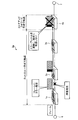
- FIG. 2 is a diagram illustrating an example of an error detection state in each transfer device when a failure occurs in the network 100 including the general transfer devices 101 to 104.
- FIG. 2 illustrates an example of an error detection state in each transfer device when a failure occurs in the network 100 including the general transfer devices 101 to 104.
- the transfer apparatus 102 detects a frame error.
- the transfer device 102 transfers the frame in which the error is detected to the next transfer device 103 as it is.
- the transfer apparatus 103 can detect an error in the frame.
- the cause of this error is due to a failure in the transmission path between the transfer apparatus 102 and the transfer apparatus 103 or due to a failure in the transmission stage before the transfer apparatus 102. It is not possible to determine whether it has been propagated.
- the transfer device 103 transfers the frame in which the error is detected to the next transfer device 104 as it is.
- the transfer device 104 can detect a frame error, but whether the cause of this error is due to a failure in the transmission path between the transfer device 103 and the transfer device 104 or a transmission stage before the transfer device 103. It is not possible to determine whether it has been propagated due to a failure. Further, the transfer device 104 cannot identify whether or not a failure has occurred in a plurality of transmission paths.
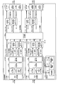
- FIG. 3 is a block diagram of a configuration example of the transfer apparatus 1 according to the first embodiment. Since the transfer apparatuses 1 to 4 have the same configuration, the transfer apparatus 1 will be described as an example.
- the transfer apparatus 1 includes input units 11-1 to 11-M, a storage unit 12, normal delay frame combination buffers 13-1 to 13-M, a switching processing unit 14, and low delay frame output buffers 15-1 to 15-1. 15-M, normal delay frame output buffers 16-1 to 16-M, and output units 17-1 to 17-M.
- the transfer device 1 includes M input ports and M output ports, but is an example, and the number of input ports and output ports is not limited to M.
- the transfer device 1 normally includes a plurality of input / output ports of two or more ports.
- the input port indicated by Rx # n and the output port indicated by Tx # n are generally one physical port, but the ports may be physically separated for input and output. Note that 1 ⁇ n ⁇ M.
- the normal delay frame combination buffers 13-1 to 13-M are referred to as normal delay frame combination buffers 13 when they are not distinguished.
- the low-delay frame output buffers 15-1 to 15-M are referred to as low-delay frame output buffers 15 when not distinguished from each other.
- the normal delay frame output buffers 16-1 to 16-M are not distinguished, they are referred to as normal delay frame output buffers 16.
- the output units 17-1 to 17-M are not distinguished, they are referred to as the output unit 17.
- the low delay frame output buffer 15 and the normal delay frame output buffer 16 may be collectively referred to as an output side buffer.
- the transfer apparatus 1 includes the input unit 11 and the normal delay frame combination buffer 13 for each input port, that is, M pieces as many as the number of input ports.
- the transfer apparatus 1 includes the low delay frame output buffer 15, the normal delay frame output buffer 16, and the output unit 17 for each output port, that is, the same number M as the number of output ports.
- a MAC Media Access Control
- IET Media Access Control
- the transfer of the normal delay frame is interrupted and the low delay frame is interrupted and transferred to satisfy the delay request of the low delay frame.
- the low-delay frame is a frame that requires low-delay transfer and is also called an express frame.
- the normal delay frame is a frame that allows a transfer delay more than a low delay frame, and is also referred to as a normal frame.
- the input unit 11 includes an FCS code calculation unit 21, an FCS check unit 22, an inversion FCS check unit 23, an error determination unit 24, and a frame identification unit 25.
- the FCS code calculation unit 21 is a calculation unit that calculates a frame check sequence code (hereinafter referred to as an FCS code) of a received frame that is a frame transferred from the previous transfer device and received by the input port.
- the FCS code calculated by the FCS code calculation unit 21 is set as the first code.
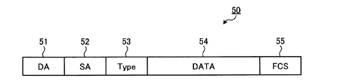
- FIG. 4 is a diagram illustrating an example of a frame format 50 of a frame transferred by the transfer apparatuses 1 to 4 according to the first embodiment.
- the frames transferred by the transfer apparatuses 1 to 4 are a low delay frame and a normal delay frame, both of which conform to the frame format 50 of the Ethernet standard.
- the frame format 50 of the frame transferred by the transfer apparatuses 1 to 4 includes a DA (Destination Address) field 51 in which the address of the frame transmission destination is stored, and an SA (Source Address) in which the address of the frame transmission source is stored.
- DA Disestination Address
- SA Source Address
- a Type field 53 storing the length of the frame, that is, a frame length
- a DATA field 54 storing user data to be transmitted
- fields from the DA field 51 to the DATA field 54 and fields from the DA field 51 to the DATA field 54.
- an FCS field 55 in which an FCS code as a check code is stored.
- the FCS code calculation unit 21 calculates the FCS code for the DA field 51, SA field 52, Type field 53, and DATA field 54 of the input frame.
- the FCS check unit 22 compares the FCS code stored in the FCS field 55 of the received frame with the FCS code calculated by the FCS code calculation unit 21, and the two compared FCS codes match or do not match It is the 1st comparison part which outputs the comparison result which shows.
- the FCS code stored in the FCS field 55 of the received frame is set as the second code.
- the comparison result output by the FCS check unit 22 is set as a first comparison result.
- the inverted FCS check unit 23 compares and compares the inverted FCS code obtained by inverting each bit of the FCS code stored in the FCS field 55 of the received frame with the FCS code calculated by the FCS code calculation unit 21. It is a second comparison unit that outputs a comparison result indicating that two FCS codes match or do not match. An inverted FCS code obtained by bit-inverting each bit of the FCS code stored in the FCS field 55 of the received frame is set as a third code. Further, the comparison result output from the inversion FCS check unit 23 is set as a second comparison result.
- the error determination unit 24 determines the error state of the received frame based on the first comparison result output from the FCS check unit 22 and the second comparison result output from the inverted FCS check unit 23. Specifically, when an error is detected in a frame, the error determination unit 24 determines whether a failure has occurred in the previous transmission path between the preceding transfer device and the own transfer device, or before the previous transfer device. It is determined whether a failure has occurred in the transmission stage or a failure location that causes an error. The error determination unit 24 outputs error determination information including the second comparison result and the FCS code calculated by the FCS code calculation unit 21.
- the frame identification unit 25 refers to the destination information 31 of the storage unit 12 based on the transmission destination address of the DA field 51 in the reception frame for the reception frame, and determines the transfer destination of the reception frame, that is, the output port that outputs the reception frame. decide.
- the frame identification unit 25 includes the source address of the SA field 52 in the received frame, service type information given to the DATA field 54 of the received frame, a VLAN (Virtual Local Area Network) tag, an Ethernet type number, and the like.
- the destination information 31 of the storage unit 12 may be used to determine the transfer destination of the received frame, that is, the output port that outputs the received frame.
- the frame identification unit 25 refers to the priority information 32 of the storage unit 12 based on the identification information given to the DATA field 54 or the like in the received frame, and determines the received frame from the priority of the received frame as a low-delay frame or Sorted into normal delay frames and output to each output port from different paths.
- the identification information in the received frame is, for example, service type information, VLAN tag, Ethernet type number, and the like.
- the frame identification unit 25 refers to the priority information 32 of the storage unit 12 using the transmission destination address of the DA field 51, the transmission source address of the SA field 52, etc. in the reception frame, and receives from the priority of the reception frame.
- the frame may be allocated to a low delay frame or a normal delay frame.
- the storage unit 12 stores destination information 31 that is referred to when the frame identification unit 25 determines a transfer destination of a received frame, that is, an output port that outputs the received frame.
- the destination information 31 indicates, for example, the relationship between the transmission destination address stored in the DA field 51 of the received frame and the output port corresponding to the route to the terminal indicated by the transmission destination address.
- the storage unit 12 stores priority information 32 that is referred to when the frame identification unit 25 determines the priority of the received frame.
- the priority information 32 indicates, for example, the relationship between the identification information stored in the DATA field 54 of the received frame and the priority corresponding to each identification information.
- the storage unit 12 is provided for the frame identification unit 25 of each of the input units 11-1 to 11-M to refer to in common.
- the 11-M frame identification unit 25 may hold information stored in the storage unit 12 therein.
- the normal delay frame combination buffers 13-1 to 13-M perform normal delay frame combination processing.
- the normal delay frame combination buffers 13-1 to 13-M are normal side delay frame input buffers for transferring the normal delay frame by the store-and-forward method.
- the combined processing of the divided normal delay frames may be completed in the transfer apparatus 1 until the output unit 17 starts output contention control with the low delay frame by IET.
- the installation positions of the normal delay frame combination buffers 13-1 to 13-M are not limited as long as the normal delay frame combination buffers 13-1 to 13-M are positioned upstream of the output unit 17. Therefore, the normal delay frame combination buffers 13-1 to 13-M may be configured to be used also as the normal delay frame output buffers 16-1 to 16-M.
- the switching processing unit 14 performs sorting, that is, switch processing, according to the transfer destination determined by the frame identification unit 25 of each input unit 11.
- the switching processing unit 14 outputs the low delay frame output from the input unit 11 to the low delay frame output buffer 15 corresponding to the output port of the transfer destination, and the normal delay frame output from the normal delay frame combination buffer 13. Is output to the normal delay frame output buffer 16 corresponding to the output port of the transfer destination. Further, the switching processing unit 14 outputs the error determination information output from the input unit 11 to the output unit 17 corresponding to the output port that is the output destination of the corresponding frame.
- the low-delay frame output buffer 15 stores low-delay frames among the received frames received at the input port.
- the low-delay frame output buffer 15 is capable of cut-through output in which frame output is started without waiting for completion of accumulation for one frame.
- the low delay frame output buffer 15 outputs the low delay frame to the output unit 17 in accordance with the output instruction from the output unit 17. Further, the low delay frame output buffer 15 stores the low delay frame when the low delay frame is input from the switching processing unit 14, that is, the low delay frame indicating that the low delay frame is received in the transfer apparatus 1. A reception notification is output to the output unit 17.
- the normal delay frame output buffer 16 stores normal delay frames among the received frames received at the input port.
- the normal delay frame output buffer 16 can perform cut-through output when a normal delay frame after being combined by the normal delay frame combining buffer 13 is input.
- the normal delay frame output buffer 16 is also used as the normal delay frame combining buffer 13 as described above, when the normal delay frame before combining is input, the store and start which starts output after the accumulation of one frame is completed. Perform forward output.
- the normal delay frame output buffer 16 outputs a normal delay frame to the output unit 17 in accordance with the output instruction from the output unit 17.
- the output unit 17 includes an output control unit 41 and an FCS update unit 42.
- the output control unit 41 preferentially outputs the low delay frame stored in the low delay frame output buffer 15 over the normal delay frame stored in the normal delay frame output buffer 16 by the IET method.
- the output control unit 41 notifies the low delay frame output buffer 15 of an output instruction when outputting a low delay frame, and notifies the normal delay frame output buffer 16 of an output instruction when outputting a normal delay frame.
- the FCS update unit 42 Based on the error determination information acquired from the switching processing unit 14, the FCS update unit 42, when the second comparison result does not match, that is, there is a failure in the previous transmission path between the previous transfer device and the own transfer device. If it occurs, when the received frame, which is a low-delay frame or a normal-delay frame to be output, is transferred to the subsequent transfer apparatus, the FCS code stored in the received frame is converted to the FCS calculated by the FCS code calculation unit 21. Each bit of the code is updated with an inverted FCS code obtained by bit-inversion. The inverted FCS code obtained by bit-inverting each bit of the FCS code calculated by the FCS code calculation unit 21 is set as a fourth code. The FCS update unit 42 uses the FCS code calculated by the FCS code calculation unit 21 included in the error determination information.
- FIG. 5 is a flowchart of the frame transfer process of the transfer apparatus 1 according to the first embodiment.
- the transfer device 1 receives a frame from a previous transfer device (not shown in FIG. 1) (step S1).
- the FCS code calculation unit 21 calculates the FCS code of the received frame (step S2).
- the FCS check unit 22 compares the second code, which is the FCS code stored in the FCS field 55 of the received frame, with the first code, which is the FCS code calculated by the FCS code calculation unit 21 (step). S3).
- the FCS check unit 22 outputs the first comparison result to the error determination unit 24.
- the inverted FCS check unit 23 includes a third code which is an inverted FCS code obtained by bit-inverting each bit of the FCS code stored in the FCS field 55 of the received frame, and the FCS code calculated by the FCS code calculation unit 21. Is compared with the first code (step S4).
- the reverse FCS check unit 23 outputs the second comparison result to the error determination unit 24.
- the error determination unit 24 Based on the first comparison result from the FCS check unit 22 and the second comparison result from the inversion FCS check unit 23, the error determination unit 24 detects an error in the received frame, that is, whether an error has occurred in the received frame. It is determined whether or not (step S5). The error determination unit 24 matches the first comparison result of the FCS check unit 22, that is, the FCS code stored in the FCS field 55 of the received frame is the same as the FCS code calculated by the FCS code calculation unit 21. It is determined that no error has occurred in the received frame.
- the error determination unit 24 that is, when the FCS code stored in the FCS field 55 of the received frame is different from the FCS code calculated by the FCS code calculation unit 21, Further, the second comparison result by the inversion FCS check unit 23 is referred to.
- the error determination unit 24 If the second comparison result by the inversion FCS check unit 23 matches, that is, if the inversion FCS code of the reception frame and the FCS code calculated by the FCS code calculation unit 21 are the same, the error determination unit 24 generates an error in the reception frame. Although it has occurred, it is determined that there is a failure in the transmission stage up to the previous transfer device, not the previous transmission line between the previous transfer device and the own transfer device.
- the error determination unit 24 It is determined that there is a failure in the previous transmission path between the device and the own transfer device.
- the error determination unit 24 outputs error determination information including the second comparison result and the FCS code calculated by the FCS code calculation unit 21 to the switching processing unit 14.
- the error determination unit 24 may not include the FCS code calculated by the FCS code calculation unit 21 in the error determination information when the second comparison result matches.
- the frame identification unit 25 refers to the destination information 31 in the storage unit 12 and determines the output port of the received frame (step S6).
- the frame identification unit 25 refers to the priority information 32 in the storage unit 12 and determines the priority of the received frame, that is, whether it is a low delay frame or a normal delay frame (step S7).
- the frame identification unit 25 outputs the low delay frame to the switching processing unit 14 when the received frame is a low delay frame (step S8: Yes).
- the frame identification unit 25 outputs the normal delay frame to the normal delay frame combination buffer 13.
- the normal delay frame combining buffer 13 combines the normal delay frames (step S9), and outputs the combined normal delay frame to the switching processing unit 14.
- the switching processing unit 14 outputs the received frame to the corresponding output buffer of the output port determined by the frame identifying unit 25 by the switch process (step S10). Specifically, the switching processing unit 14 outputs the low delay frame to the low delay frame output buffer 15 corresponding to the output port determined by the frame identification unit 25, and outputs the normal delay frame determined by the frame identification unit 25. The data is output to the normal delay frame output buffer 16 corresponding to the port. Further, the switching processing unit 14 outputs the error determination information to the output unit 17 corresponding to the output port determined by the frame identification unit 25 by the switching process.
- the low-delay frame output buffer 15 stands by until an output instruction is issued from the output control unit 41 of the output unit 17 (step S11: No), and when there is an output instruction from the output control unit 41 (step S11: Yes), the low delay frame output buffer 15 A delay frame is output (step S12).
- the normal delay frame output buffer 16 waits until there is an output instruction from the output control unit 41 (step S11: No), and when there is an output instruction from the output control unit 41 (step S11: Yes), the normal delay A frame is output (step S12).
- the output control unit 41 performs frame output control by notifying each output buffer of an output instruction so that a low delay frame is preferentially output over a normal delay frame by the IET method as described above. .
- the FCS update unit 42 of the output unit 17 performs bit inversion on each bit of the FCS code calculated by the FCS code calculation unit 21 when the second comparison result does not match (step S13: Yes).
- the FCS code in the FCS field 55 of the low delay frame or the normal delay frame is updated with the inverted FCS code thus made (step S14).
- the output control unit 41 outputs, that is, transfers the low delay frame or the normal delay frame from the output port to the subsequent transfer device (step S15).
- the FCS update unit 42 does not update the FCS code when the second comparison result is the same (step S13: No). In this case, the output unit 17 omits the process of step S14, and the output control unit 41 outputs, that is, transfers, the low delay frame or the normal delay frame from the output port to the subsequent transfer device (step S15).
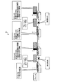
- FIG. 6 is a diagram illustrating an example of an error detection state in each of the transfer apparatuses 1 to 4 when a failure occurs in a plurality of transmission paths in the network 5 of the first embodiment.
- the calculated FCS code and the received frame
- the transfer device 1 transfers the frame as it is without updating the FCS code in the FCS field 55 because the calculated FCS code matches the FCS code in the FCS field 55 of the received frame.
- the transfer device 2 does not match the calculated FCS code with the FCS code in the FCS field 55 of the received frame, and the inverted FCS code obtained by bit-inverting each bit of the calculated FCS code and the FCS code in the FCS field 55 of the received frame Therefore, it is determined that a failure has occurred in the immediately preceding transmission line.
- the transfer device 2 transfers the frame by updating the FCS code in the FCS field 55 with the inverted FCS code obtained by inverting each bit of the calculated FCS code.
- the transfer apparatus 3 does not match the calculated FCS code with the FCS code in the FCS field 55 of the received frame, and the inverted FCS code obtained by bit-inverting each bit of the calculated FCS code and the FCS code in the FCS field 55 of the received frame Therefore, it is determined that a failure has occurred in the transmission stage before the transfer device 2, but no failure has occurred in the immediately preceding transmission line.
- the transfer apparatus 3 determines that the frame error has been propagated due to a failure in the transmission stage prior to the transfer apparatus 2, and transfers the frame as it is without updating the FCS code in the FCS field 55.
- the transfer device 4 does not match the calculated FCS code with the FCS code in the FCS field 55 of the received frame, and the inverted FCS code obtained by bit-inverting each bit of the calculated FCS code and the FCS code in the FCS field 55 of the received frame Therefore, it is determined that a failure has occurred in the immediately preceding transmission line.
- the transfer device 4 transfers the frame by updating the FCS code in the FCS field 55 with the inverted FCS code obtained by inverting each bit of the calculated FCS code.
- each of the transfer apparatuses 1 to 4 can detect an error and distinguish whether the cause of the error is a failure in the previous transmission path or a propagation error.
- the network 5 can detect the location where the error has occurred, that is, which transmission path between the transfer devices is the cause.
- the transfer apparatus 1 Since the transfer apparatuses 1 to 4 have the same configuration, the transfer apparatus 1 will be described as an example.
- the input unit 11, the storage unit 12, the normal delay frame combination buffer 13, the switching processing unit 14, the low delay frame output buffer 15, the normal delay frame output buffer 16, and the output unit 17 are realized by a processing circuit. The That is, the transfer apparatus 1 calculates the FCS code of the received frame, compares the FCS code in the received frame with the calculated FCS code, and inverts FCS obtained by bit-inverting each bit of the FCS code in the received frame.
- the code is compared with the calculated FCS code, and if it is determined that an error has been detected in the frame due to a failure in the previous transmission path between the previous transfer device and the own transfer device, the FCS code of the frame is updated and output
- a processing circuit is provided.
- the processing circuit may be dedicated hardware, a CPU (Central Processing Unit) that executes a program stored in the memory, and a memory.
- CPU Central Processing Unit
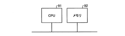
- FIG. 7 is a diagram illustrating an example in which the processing circuit of the transfer apparatus 1 according to the first embodiment is configured by a CPU and a memory.
- the processing circuit includes the CPU 91 and the memory 92
- each function of the transfer device 1 is realized by software, firmware, or a combination of software and firmware.
- Software or firmware is described as a program and stored in the memory 92.
- each function is realized by the CPU 91 reading and executing the program stored in the memory 92. That is, in the transfer device 1, the input unit 11, the storage unit 12, the normal delay frame combination buffer 13, the switching processing unit 14, the low delay frame output buffer 15, the normal delay frame output buffer 16, and the output unit 17 are executed by a processing circuit.
- a step of calculating the FCS code of the received frame a step of comparing the FCS code in the received frame with the calculated FCS code, an inverted FCS in which each bit of the FCS code in the received frame is bit-inverted
- a step of comparing the code with the calculated FCS code and if it is determined that an error has been detected in the frame due to a failure in the previous transmission path between the previous transfer device and the own transfer device, the FCS code of the frame is updated.
- the CPU 91 may be a processing device, an arithmetic device, a microprocessor, a microcomputer, a processor, a DSP (Digital Signal Processor), or the like.
- the memory 92 is a nonvolatile or volatile semiconductor memory such as RAM (Random Access Memory), ROM (Read Only Memory), flash memory, EPROM (Erasable Programmable ROM), EEPROM (Electrically EPROM), etc. Magnetic disks, flexible disks, optical disks, compact disks, mini disks, DVDs (Digital Versatile Discs), etc. are applicable.
- FIG. 8 is a diagram illustrating an example in which the processing circuit of the transfer device 1 according to the first embodiment is configured with dedicated hardware.
- the processing circuit is dedicated hardware
- the processing circuit 93 shown in FIG. 8 includes, for example, a single circuit, a composite circuit, a programmed processor, a parallel programmed processor, an ASIC (Application Specific Integrated Circuit), an FPGA (FPGA). Field Programmable Gate Array) or a combination of these.
- Each function of the transfer device 1 may be realized by the processing circuit 93 for each function, or each function may be realized by the processing circuit 93 collectively.
- each function of the transfer device 1 may be realized by dedicated hardware and a part may be realized by software or firmware.
- the processing circuit can realize the above-described functions by dedicated hardware, software, firmware, or a combination thereof.
- the transfer apparatuses 1 to 4 calculate the FCS code of the received frame, compare the FCS code in the received frame with the calculated FCS code, and The inverted FCS code obtained by inverting each bit of the FCS code in the received frame is compared with the calculated FCS code, and based on each comparison result, the immediately preceding transmission path between the transfer device at the previous stage and the own transfer device
- the FCS code of the frame is updated and output.
- the network 5 does not delay the transfer of the frame. It is possible to detect whether the transmission path between transfer devices is the cause.
- Embodiment 2 FIG. In the first embodiment, all of the transfer devices 1 to 4 in the network 5 have the functions described in the first embodiment, that is, devices that can use an inverted FCS code. In the second embodiment, a case will be described in which a network includes a terminal that cannot use an inverted FCS code. A different part from Embodiment 1 is demonstrated.
- FIG. 9 is a block diagram of a configuration example of the transfer device 1a according to the second embodiment.
- the transfer device 1a deletes the input units 11-1 to 11-M, the storage unit 12, the normal delay frame combination buffers 13-1 to 13-M, and the switching processing unit 14 from the transfer device 1, 11a-1 to 11a-M, a storage unit 12a, normal delay frame combination buffers 13a-1 to 13a-M, a switching processing unit 14a, and low delay frame input buffers 18-1 to 18-M.
- the input units 11a-1 to 11a-M are not distinguished, they are referred to as the input unit 11a.
- the normal delay frame combination buffers 13a-1 to 13a-M are not distinguished, they are referred to as normal delay frame combination buffers 13a.
- the low-delay frame input buffers 18-1 to 18-M are not distinguished, they are referred to as low-delay frame input buffers 18.
- the transfer device 1a includes the input unit 11a, the normal delay frame combination buffer 13a, and the low delay frame input buffer 18 for each input port, that is, the same M as the input ports.
- the input unit 11a is obtained by replacing the input determination unit 11 with the error determination unit 24 and the frame identification unit 25 with an error determination unit 24a and a frame identification unit 25a.
- the error determination unit 24a performs the same operation as the error determination unit 24. However, when an error is detected in the received frame, that is, when the first comparison result does not match, it indicates that an error has occurred in the received frame. An error signal is output.
- the frame identification unit 25a refers to the connection device information 33 in the storage unit 12a based on the transmission destination address of the DA field 51 in the frame, and outputs the frame transfer destination, that is, the frame It is determined whether or not a subsequent apparatus connected to the output port is compatible with the processing of the first embodiment. Specifically, the frame identification unit 25a determines whether or not an inverted FCS code obtained by bit-inverting each bit of the FCS code stored in the FCS field 55 of the received frame can be used. Note that the frame identification unit 25 uses the transmission source address of the SA field 52 in the frame, the service type information given to the DATA field 54 of the frame, the VLAN tag, the Ethernet type number, etc. to connect the storage unit 12a.
- the frame identification unit 25a when a device connected to an output port that outputs a frame cannot use an inverted FCS code, sends an error signal from the error determination unit 24a to a normal delay frame combination buffer that is a frame output destination. 13a or the low delay frame input buffer 18.
- connection device information 33 is stored.
- the connection device information 33 indicates, for example, a correspondence relationship between the transmission destination address stored in the DA field 51 of the frame and whether or not the terminal indicated by the transmission destination address can use the inverted FCS code.
- the low-delay frame input buffers 18-1 to 18-M transfer the low-delay frame by a store-and-forward method when transferring the low-delay frame to a subsequent apparatus that cannot use the inverted FCS code. Store temporarily.
- the low delay frame input buffers 18-1 to 18-M are input side buffers for low delay frames. Further, when the low delay frame input buffers 18-1 to 18-M obtain the error signal together with the low delay frame from the input unit 11a, they are discarded without outputting the low delay frame.
- the normal delay frame combination buffers 13a-1 to 13a-M discard the error signal without outputting the normal delay frame when the error signal is acquired together with the normal delay frame from the input unit 11a. To do.
- the normal delay frame combination buffers 13a-1 to 13a-M are input side buffers for normal delay frames.
- the switching processing unit 14a In addition to the function of the switching processing unit 14, the switching processing unit 14a outputs the low delay frame input from the low delay frame input buffer 18 to the low delay frame output buffer 15 corresponding to the output port of the transfer destination.
- the transfer device 1a transfers the low-delay frame by cut-through as in the first embodiment.
- the transfer device 1a transfers the low-delay frame by the store-and-forward method through the low-delay frame input buffer 18 unlike the first embodiment. .
- FIG. 10 is a flowchart of the frame transfer process of the transfer device 1a according to the second embodiment.
- the processing from step S1 to step S8 is the same as the processing in the first embodiment shown in FIG.
- the frame identifying unit 25a determines whether the device connected to the output port of the output destination of the low-delay frame is a device that can use the inverted FCS code. Is determined (step S21). In the case of a device that can use the inverted FCS code (step S21: Yes), the frame identification unit 25a outputs a low-delay frame to the switching processing unit 14a. In the case of a device that cannot use the inverted FCS code (step S21: No), the frame identification unit 25a outputs the low delay frame to the low delay frame input buffer 18.
- the low delay frame input buffer 18 determines whether an error is detected in the low delay frame (step S22). When the error signal is not acquired together with the low delay frame, the low delay frame input buffer 18 determines that no error is detected in the low delay frame (step S22: No), and sends the low delay frame to the switching processing unit 14a. Output. When the error signal is acquired together with the low delay frame, the low delay frame input buffer 18 determines that an error has been detected in the low delay frame (step S22: Yes), and discards the low delay frame (step S23).
- the normal delay frame combining buffer 13a combines the normal delay frames (step S9), and determines whether an error is detected in the normal delay frame (step S24). .
- the normal delay frame combination buffer 13a determines that no error is detected in the normal delay frame (step S24: No), and sends the normal delay frame to the switching processing unit 14a. Output.
- the normal delay frame combination buffer 13a determines that an error has been detected in the normal delay frame (step S24: Yes), and discards the normal delay frame (step S25).
- step S10 to step S15 is the same as the processing in the first embodiment shown in FIG.
- the frame identification unit 25a of the input unit 11a is low when the device connected to the output port of the transfer destination of the frame determined as the low delay frame is a device that can use the inverted FCS code.
- the delay frame is output to the switching processing unit 14a and transferred by the cut-through method.
- the frame identification unit 25a outputs the low delay frame to the low delay frame input buffer 18 when the device connected to the output port of the transfer destination of the frame determined as the low delay frame cannot use the inverted FCS code. And store and forward.
- the frame identifying unit 25a converts the normal delay frame into the normal delay frame combining buffer 13a for the normal delay frame regardless of whether or not the device connected to the output port of the frame transfer destination can use the inverted FCS code. And transfer in a store-and-forward manner.
- the frame identification unit 25a determines an error in the error determination unit 24a, and, for a frame in which the device connected to the transfer destination output port cannot use the inverted FCS code, the error signal is sent to the low delay frame input buffer together with the frame. 18 or the normal delay frame combination buffer 13a.
- the low delay frame input buffer 18 discards the low delay frame when the error signal is acquired together with the low delay frame.
- the normal delay frame combination buffer 13a discards the normal delay frame.
- FIG. 11 is a diagram illustrating an example of the frame transfer operation of the transfer apparatuses 1a to 4a when the network 5a according to the second embodiment includes the terminals 6 and 7 that cannot use the inverted FCS code.
- a terminal 6 that cannot use the inverted FCS code is connected to the front stage of the transfer apparatus 1a
- a terminal 7 that cannot use the inverted FCS code is connected to the rear stage of the transfer apparatus 4a.
- the operations of the transfer apparatuses 1a to 3a are the same as those of the transfer apparatuses 1 to 3 shown in FIG. That is, the transfer apparatuses 1a to 3a transfer frames by the cut-through method.
- the transfer device 4a transfers the low-delay frame that should be transferred by the cut-through method by the store-and-forward method. Since the transfer device 4a transfers the low-delay frame by the store-and-forward method, when an error is detected in the low-delay frame scheduled to be transferred to the terminal 7, the low-delay frame in which the error is detected is transferred to the terminal 7. It becomes possible to discard it. Since the transfer device 4a transfers the normal delay frame by the store-and-forward method as in the first embodiment, an error is detected when an error is detected in the normal delay frame scheduled to be transferred to the terminal 7. The normal delay frame is discarded without being transferred to the terminal 7. Thus, the transfer device 4a discards the frame in which the error is detected and does not transfer it to the terminal 7.
- the hardware configuration of the transfer apparatuses 1a to 4a is realized by the same hardware configuration as that of the transfer apparatuses 1 to 4.
- the transfer apparatuses 1a to 4a cannot use the inverted FCS code described in the first embodiment by a device connected to a subsequent stage.
- the low-delay frame is also transferred by the store and forward method.
- the transfer apparatuses 1a to 4a can discard the frame without transferring it when an error is detected in the low delay frame and the normal delay frame.
- the configuration described in the above embodiment shows an example of the contents of the present invention, and can be combined with another known technique, and can be combined with other configurations without departing from the gist of the present invention. It is also possible to omit or change the part.
- 1 to 4a transfer device 5, 5a network, 6, 7 terminal, 11-1 to 11-M, 11a-1 to 11a-M input unit, 12, 12a storage unit, 13-1 to 13- M, 13a-1 to 13a-M normal delay frame combination buffer, 14, 14a switching processing unit, 15-1 to 15-M low delay frame output buffer, 16-1 to 16-M normal delay frame output buffer, 17- 1-17-M output section, 18-1-18-M low delay frame input buffer, 21 FCS code calculation section, 22 FCS check section, 23 inverted FCS check section, 24, 24a error determination section, 25, 25a frame identification Part, 31 destination information, 32 priority information, 33 connection device information, 41 output control part, 42 FCS update part.
Landscapes
- Engineering & Computer Science (AREA)
- Computer Networks & Wireless Communication (AREA)
- Signal Processing (AREA)
- Environmental & Geological Engineering (AREA)
- Quality & Reliability (AREA)
- Small-Scale Networks (AREA)
- Data Exchanges In Wide-Area Networks (AREA)
- Detection And Prevention Of Errors In Transmission (AREA)
Abstract
Priority Applications (6)
| Application Number | Priority Date | Filing Date | Title |
|---|---|---|---|
| KR1020197011106A KR102024521B1 (ko) | 2016-10-26 | 2016-10-26 | 전송 장치 및 프레임 전송 방법 |
| US16/338,269 US11115304B2 (en) | 2016-10-26 | 2016-10-26 | Transfer device and frame transfer method |
| CN201680090208.4A CN109891833B (zh) | 2016-10-26 | 2016-10-26 | 传送装置和帧传送方法 |
| JP2018546991A JP6494880B2 (ja) | 2016-10-26 | 2016-10-26 | 転送装置およびフレーム転送方法 |
| PCT/JP2016/081756 WO2018078747A1 (fr) | 2016-10-26 | 2016-10-26 | Dispositif de transfert et procédé de transfert de trame |
| TW106109506A TWI627844B (zh) | 2016-10-26 | 2017-03-22 | 轉傳裝置及數據包轉傳方法 |
Applications Claiming Priority (1)
| Application Number | Priority Date | Filing Date | Title |
|---|---|---|---|
| PCT/JP2016/081756 WO2018078747A1 (fr) | 2016-10-26 | 2016-10-26 | Dispositif de transfert et procédé de transfert de trame |
Publications (1)
| Publication Number | Publication Date |
|---|---|
| WO2018078747A1 true WO2018078747A1 (fr) | 2018-05-03 |
Family
ID=62024512
Family Applications (1)
| Application Number | Title | Priority Date | Filing Date |
|---|---|---|---|
| PCT/JP2016/081756 Ceased WO2018078747A1 (fr) | 2016-10-26 | 2016-10-26 | Dispositif de transfert et procédé de transfert de trame |
Country Status (6)
| Country | Link |
|---|---|
| US (1) | US11115304B2 (fr) |
| JP (1) | JP6494880B2 (fr) |
| KR (1) | KR102024521B1 (fr) |
| CN (1) | CN109891833B (fr) |
| TW (1) | TWI627844B (fr) |
| WO (1) | WO2018078747A1 (fr) |
Families Citing this family (2)
| Publication number | Priority date | Publication date | Assignee | Title |
|---|---|---|---|---|
| JP6605177B2 (ja) * | 2017-03-06 | 2019-11-13 | 三菱電機株式会社 | 転送装置、転送方法及び転送システム |
| US12425924B2 (en) * | 2019-10-23 | 2025-09-23 | Lg Electronics Inc. | Technique for performing low latency communication in wireless LAN system |
Citations (5)
| Publication number | Priority date | Publication date | Assignee | Title |
|---|---|---|---|---|
| US6091707A (en) * | 1997-12-18 | 2000-07-18 | Advanced Micro Devices, Inc. | Methods and apparatus for preventing under-flow conditions in a multiple-port switching device |
| JP4308297B2 (ja) * | 2005-05-09 | 2009-08-05 | 三菱電機株式会社 | 通信装置およびスイッチ処理装置 |
| US20110022935A1 (en) * | 2006-10-17 | 2011-01-27 | Mcdaniel Scott | Method and System for Interlocking Data Integrity for Network Adapters |
| US20130016724A1 (en) * | 2011-07-17 | 2013-01-17 | Broadcom Corporation | Link layer preemption |
| US20150347218A1 (en) * | 2014-05-29 | 2015-12-03 | Freescale Semiconductor, Inc. | Indicating internal transmitter errors in a controller area network (can) |
Family Cites Families (9)
| Publication number | Priority date | Publication date | Assignee | Title |
|---|---|---|---|---|
| US4577313A (en) * | 1984-06-04 | 1986-03-18 | Sy Kian Bon K | Routing mechanism with encapsulated FCS for a multi-ring local area network |
| US8295303B2 (en) * | 2001-03-30 | 2012-10-23 | Verizon Business Global Llc | System and method for transmission of frame relay communications over a digital subscriber line equipped with asynchronous transfer mode components |
| US8001248B1 (en) * | 2001-07-13 | 2011-08-16 | Cisco Technology, Inc. | System and method for providing quality of service to DSL internet connections |
| JP3883562B2 (ja) * | 2003-08-20 | 2007-02-21 | 日本電信電話株式会社 | パケット通信方法およびパケット通信装置 |
| EP1657888A1 (fr) * | 2004-11-16 | 2006-05-17 | Abb Research Ltd. | Réception de trames redondantes et non redondantes |
| JP2009284024A (ja) * | 2008-05-19 | 2009-12-03 | Fujitsu Ltd | フレーム伝送装置およびフレーム伝送方法 |
| US20100309908A1 (en) * | 2009-06-08 | 2010-12-09 | Hewlett-Packard Development Company, L.P. | Method and system for communicating with a network device |
| JP2012034047A (ja) * | 2010-07-28 | 2012-02-16 | Mitsubishi Electric Corp | 中継装置及びコンピュータプログラム及び中継方法 |
| CN105187209B (zh) * | 2015-07-21 | 2018-07-13 | 中国航天科工集团第三研究院第八三五七研究所 | 一种以太网通信安全保护的方法 |
-
2016
- 2016-10-26 US US16/338,269 patent/US11115304B2/en active Active
- 2016-10-26 JP JP2018546991A patent/JP6494880B2/ja active Active
- 2016-10-26 CN CN201680090208.4A patent/CN109891833B/zh active Active
- 2016-10-26 WO PCT/JP2016/081756 patent/WO2018078747A1/fr not_active Ceased
- 2016-10-26 KR KR1020197011106A patent/KR102024521B1/ko active Active
-
2017
- 2017-03-22 TW TW106109506A patent/TWI627844B/zh active
Patent Citations (5)
| Publication number | Priority date | Publication date | Assignee | Title |
|---|---|---|---|---|
| US6091707A (en) * | 1997-12-18 | 2000-07-18 | Advanced Micro Devices, Inc. | Methods and apparatus for preventing under-flow conditions in a multiple-port switching device |
| JP4308297B2 (ja) * | 2005-05-09 | 2009-08-05 | 三菱電機株式会社 | 通信装置およびスイッチ処理装置 |
| US20110022935A1 (en) * | 2006-10-17 | 2011-01-27 | Mcdaniel Scott | Method and System for Interlocking Data Integrity for Network Adapters |
| US20130016724A1 (en) * | 2011-07-17 | 2013-01-17 | Broadcom Corporation | Link layer preemption |
| US20150347218A1 (en) * | 2014-05-29 | 2015-12-03 | Freescale Semiconductor, Inc. | Indicating internal transmitter errors in a controller area network (can) |
Also Published As
| Publication number | Publication date |
|---|---|
| CN109891833B (zh) | 2021-06-08 |
| KR20190047082A (ko) | 2019-05-07 |
| TW201817201A (zh) | 2018-05-01 |
| US20190319865A1 (en) | 2019-10-17 |
| JP6494880B2 (ja) | 2019-04-03 |
| TWI627844B (zh) | 2018-06-21 |
| CN109891833A (zh) | 2019-06-14 |
| KR102024521B1 (ko) | 2019-09-24 |
| JPWO2018078747A1 (ja) | 2019-03-14 |
| US11115304B2 (en) | 2021-09-07 |
Similar Documents
| Publication | Publication Date | Title |
|---|---|---|
| US10528498B2 (en) | Transfer apparatus and frame transfer method | |
| RU2540815C2 (ru) | Прерывание, по меньшей мере частичное, передачи кадра | |
| US10469200B2 (en) | Minimum latency link layer metaframing and error correction | |
| US20130114593A1 (en) | Reliable Transportation a Stream of Packets Using Packet Replication | |
| WO2016057379A1 (fr) | Validation de trajet inverse pour des réseaux routés par source | |
| US20220377015A1 (en) | Designated forwarder selection for multihomed hosts in an ethernet virtual private network | |
| US20100128726A1 (en) | Data transmitter and data transmission method | |
| US20200044964A1 (en) | Defect detection in ip/mpls network tunnels | |
| JP5702708B2 (ja) | パケット制御方法及びパケット制御装置 | |
| JP6494880B2 (ja) | 転送装置およびフレーム転送方法 | |
| US20180069790A1 (en) | Packet transfer device and packet transfer method | |
| CN103516631A (zh) | 通信装置 | |
| KR101576833B1 (ko) | 이중화 장치에서 수신 버퍼를 이용한 통신 데이터의 중복 검사 방법 | |
| US9391791B2 (en) | Preprocessing unit for network data | |
| JP6907835B2 (ja) | 計算ノード装置、並列計算機システム、および計算ノード装置の制御方法 | |
| JP6219233B2 (ja) | 無瞬断切替装置および無瞬断切替方法 | |
| JP2015231210A (ja) | パケット転送装置およびパケット転送方法 | |
| JP5548147B2 (ja) | 伝送装置及び伝送網システム | |
| JP7547789B2 (ja) | 中継装置 | |
| CN108023660A (zh) | 一种光传送网络业务接入方法及装置 | |
| WO2025161854A1 (fr) | Procédé de communication, appareil de communication et dispositif de communication | |
| CN117675719A (zh) | 队列调度方法及装置 | |
| JP2020039044A (ja) | 通信システム |
Legal Events
| Date | Code | Title | Description |
|---|---|---|---|
| 121 | Ep: the epo has been informed by wipo that ep was designated in this application |
Ref document number: 16919824 Country of ref document: EP Kind code of ref document: A1 |
|
| ENP | Entry into the national phase |
Ref document number: 2018546991 Country of ref document: JP Kind code of ref document: A |
|
| ENP | Entry into the national phase |
Ref document number: 20197011106 Country of ref document: KR Kind code of ref document: A |
|
| NENP | Non-entry into the national phase |
Ref country code: DE |
|
| 122 | Ep: pct application non-entry in european phase |
Ref document number: 16919824 Country of ref document: EP Kind code of ref document: A1 |