WO2018092580A1 - Capteur de courant - Google Patents
Capteur de courant Download PDFInfo
- Publication number
- WO2018092580A1 WO2018092580A1 PCT/JP2017/039307 JP2017039307W WO2018092580A1 WO 2018092580 A1 WO2018092580 A1 WO 2018092580A1 JP 2017039307 W JP2017039307 W JP 2017039307W WO 2018092580 A1 WO2018092580 A1 WO 2018092580A1
- Authority
- WO
- WIPO (PCT)
- Prior art keywords
- magnetic sensor
- current
- conductor
- bridge circuit
- sensor
- Prior art date
- Legal status (The legal status is an assumption and is not a legal conclusion. Google has not performed a legal analysis and makes no representation as to the accuracy of the status listed.)
- Ceased
Links
Images


Classifications
-
- G—PHYSICS
- G01—MEASURING; TESTING
- G01R—MEASURING ELECTRIC VARIABLES; MEASURING MAGNETIC VARIABLES
- G01R15/00—Details of measuring arrangements of the types provided for in groups G01R17/00 - G01R29/00, G01R33/00 - G01R33/26 or G01R35/00
- G01R15/14—Adaptations providing voltage or current isolation, e.g. for high-voltage or high-current networks
- G01R15/20—Adaptations providing voltage or current isolation, e.g. for high-voltage or high-current networks using galvano-magnetic devices, e.g. Hall-effect devices, i.e. measuring a magnetic field via the interaction between a current and a magnetic field, e.g. magneto resistive or Hall effect devices
-
- G—PHYSICS
- G01—MEASURING; TESTING
- G01R—MEASURING ELECTRIC VARIABLES; MEASURING MAGNETIC VARIABLES
- G01R19/00—Arrangements for measuring currents or voltages or for indicating presence or sign thereof
Definitions
- the present invention relates to a current sensor.
- Patent Document 1 JP-A-2014-55839 is a prior document disclosing the configuration of the current detection device.
- the current detection device described in Patent Document 1 is based on a conducting wire through which a current flows, a substrate on which an insertion portion to be inserted in a state in which at least a part of the conducting wire penetrates, and a current that is mounted on the substrate and flows through the conducting wire. And a pair of magnetic detection elements for detecting magnetic flux generated around the conducting wire.
- Patent Document 2 JP-A-6-148301 (Patent Document 2) as a prior document disclosing the configuration of a magnetic sensor.
- the magnetic sensor described in Patent Document 2 includes a bias magnetic field generation unit made of a hard magnetic film and a magnetoresistive element made of a ferromagnetic thin film formed on the same chip.
- the bias magnetic field generation unit the two thin film magnets are spaced apart from each other so that the different polarities face each other.
- the magnetoresistive element is disposed near the center of the magnetic field formed by the two thin film magnets.
- the current sensor cannot be reduced in size.
- the present invention has been made in view of the above problems, and an object thereof is to provide a current sensor that is miniaturized.
- the current sensor according to the present invention includes a conductor, a first magnetic sensor, a second magnetic sensor, and a pair of bias magnets.
- the conductor has a longitudinal direction, one main surface, and the other main surface located on the side opposite to the one main surface.
- the conductor is made of a nonmagnetic material.
- a current to be measured flows through the conductor.
- the first magnetic sensor is disposed on the one main surface.
- the first magnetic sensor detects the strength of the magnetic field generated by the current to be measured flowing through the conductor.
- the second magnetic sensor is disposed on the other main surface so as to face the first magnetic sensor with a conductor interposed therebetween.
- the second magnetic sensor detects the strength of the magnetic field generated by the current to be measured flowing through the conductor.
- the pair of bias magnets are spaced from each other in the longitudinal direction.
- the pair of bias magnets applies a bias magnetic field to the first magnetic sensor and the second magnetic sensor.
- the conductor has a flat portion extending in the longitudinal direction, and a pair of extending portions extending bent from both ends of the flat portion in the longitudinal direction toward the other main surface.
- Each of the first magnetic sensor and the second magnetic sensor is located along the flat portion.
- a flat portion is located between the two, and the center of each of the pair of bias magnets in the height direction perpendicular to the one main surface of the flat portion is the height direction. In FIG. 4, the flat portion is located within a range.
- the center of the flat portion in the height direction is located on an imaginary line connecting the centers of the pair of bias magnets in the height direction.
- each of the first magnetic sensor and the second magnetic sensor includes a plurality of magnetoresistive elements constituting a bridge circuit, and the output voltage of the bridge circuit of the first magnetic sensor and the second magnetic sensor.
- An IC (Integrated Circuit) chip having a calculation unit for calculating the value of the current to be measured by calculating the output voltage of the bridge circuit is included.
- the plurality of magnetoresistive elements are formed on the IC chip.
- the IC chip faces the flat portion in each of the first magnetic sensor and the second magnetic sensor.
- the phase of the output voltage of the bridge circuit of the first magnetic sensor and the phase of the output voltage of the bridge circuit of the second magnetic sensor with respect to the magnetic field generated by the current to be measured flowing through the conductor are in reverse phase.
- the calculation unit is a subtractor or a differential amplifier.
- the phase of the output voltage of the bridge circuit of the first magnetic sensor and the phase of the output voltage of the bridge circuit of the second magnetic sensor with respect to the magnetic field generated by the current to be measured flowing through the conductor. are in phase.
- the calculation unit is an adder or an addition amplifier.
- the conductor, the first magnetic sensor, the second magnetic sensor, and the pair of bias magnets are integrated with a sealing resin.
- the current sensor can be reduced in size.
- FIG. 3 is a cross-sectional view of the current sensor of FIG. 2 as viewed from the direction of arrows III-III. It is a circuit diagram which shows the bridge circuit which the some magnetoresistive element of each of a 1st magnetic sensor and a 2nd magnetic sensor comprises. It is a circuit diagram which shows the circuit structure of the current sensor which concerns on Embodiment 1 of this invention.
- FIG. 6 is a graph showing the relationship between the output voltage ((V +) ⁇ (V ⁇ )) (mV) from each bridge circuit of the first magnetic sensor and the second magnetic sensor and the strength (mT) of the applied magnetic field. .
- the external magnetic field is applied to the first magnetic sensor and the second magnetic sensor, the value of the current to be measured flowing through the conductor, the output voltage of each bridge circuit of the first magnetic sensor and the second magnetic sensor, It is a graph which shows the relationship.
- FIG. 1 is a side view showing a configuration of a current sensor according to Embodiment 1 of the present invention.
- FIG. 2 is a plan view of the current sensor of FIG. 1 viewed from the direction of arrow II.
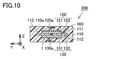
- FIG. 3 is a cross-sectional view of the current sensor of FIG. 2 as viewed from the direction of arrows III-III. 1 to 3, the longitudinal direction of a conductor 110 described later is illustrated as an X-axis direction, the width direction of the conductor 110 is defined as a Y-axis direction, and the height direction is illustrated as a Z-axis direction.
- the current sensor 100 includes a conductor 110, a first magnetic sensor 120, a second magnetic sensor 130, and a pair of bias magnets.
- the pair of bias magnets includes a first bias magnet 140 and a second bias magnet 150.
- the conductor 110 has a longitudinal direction (X-axis direction), one main surface 111, and the other main surface 112 located on the opposite side of the one main surface 111.
- the conductor 110 includes a flat portion 113 extending in the longitudinal direction (X-axis direction) and a pair of curved portions extending from both ends of the flat portion 113 in the longitudinal direction (X-axis direction) to the other main surface 112 side. Has an extension.
- the direction orthogonal to one main surface 111 of the flat portion 113 is the height direction (Z-axis direction).
- the direction orthogonal to each of the longitudinal direction (X-axis direction) and the height direction (Z-axis direction) of the conductor 110 is the width direction (Y-axis direction) of the conductor 110.
- the width of the conductor 110 is substantially constant.
- the pair of extending portions includes a first extending portion 114 that bends and extends from one end in the longitudinal direction (X-axis direction) of the flat portion 113 to the other main surface 112 side, and a longitudinal direction (X The second extending portion 115 is bent and extends from the other end in the axial direction to the other main surface 112 side.
- each of the first extending portion 114 and the second extending portion 115 extends along the height direction (Z-axis direction).
- the length of the first extending portion 114 and the length of the second extending portion 115 in the height direction (Z-axis direction) are substantially the same.
- the conductor 110 includes a first flat portion 116 extending from one end of the first extending portion 114 toward one side in the longitudinal direction (X-axis direction) and a longitudinal direction (X It further has a second flat portion 117 extending toward the other side in the axial direction.
- the extending direction of each of the first flat portion 116 and the second flat portion 117 is parallel to the extending direction of the flat portion 113.
- the conductor 110 does not necessarily have the first flat portion 116 and the second flat portion 117, and it is sufficient that the conductor 110 has at least the flat portion 113 and a pair of extending portions.
- a current 1 to be measured flows through the conductor 110.
- the current 1 to be measured is measured from the end of the conductor 110 on one side in the longitudinal direction (X-axis direction) toward the end of the conductor 110 on the other side in the longitudinal direction (X-axis direction). Flowing.
- the conductor 110 is made of a nonmagnetic material.
- the conductor 110 is made of copper.
- the material of the conductor 110 is not limited to copper, and may be a nonmagnetic material such as gold, silver, or aluminum.
- the conductor 110 is formed by pressing a thin plate.
- the method of forming the conductor 110 is not limited to this, and cutting or casting may be used.
- the first magnetic sensor 120 detects the strength of the magnetic field generated by the current 1 to be measured flowing through the conductor 110.
- the first magnetic sensor 120 is disposed on one main surface 111 of the conductor 110.
- the first magnetic sensor 120 is located along the flat portion 113.
- the first magnetic sensor 120 is in contact with one main surface 111 of the flat portion 113 with an insulating film (not shown) interposed therebetween.
- the first magnetic sensor 120 is fixed to the conductor 110 by die bonding.
- the first magnetic sensor 120 includes a plurality of magnetoresistive elements 121 and an IC chip 122.
- the plurality of magnetoresistive elements 121 are formed on the IC chip 122.
- the plurality of magnetoresistive elements 121 include patterned magnetoresistive films made of a ferromagnetic material such as permalloy.
- the IC chip 122 faces the flat part 113.
- the second magnetic sensor 130 detects the strength of the magnetic field generated by the current 1 to be measured flowing through the conductor 110.
- the second magnetic sensor 130 is disposed on the other main surface 112 of the conductor 110 so as to face the first magnetic sensor 120 with the conductor 110 interposed therebetween.
- the second magnetic sensor 130 is located along the flat portion 113. In the present embodiment, the second magnetic sensor 130 is in contact with the other main surface 112 of the flat portion 113 with an insulating film (not shown) interposed therebetween.
- the second magnetic sensor 130 is fixed to the conductor 110 by die bonding.
- the second magnetic sensor 130 includes a plurality of magnetoresistive elements 131 and an IC chip 132.
- the plurality of magnetoresistive elements 131 are formed on the IC chip 132.
- the plurality of magnetoresistive elements 131 include a patterned magnetoresistive film made of a ferromagnetic material such as permalloy.
- the IC chip 132 is opposed to the flat portion 113.
- FIG. 4 is a circuit diagram showing a bridge circuit formed by a plurality of magnetoresistive elements of each of the first magnetic sensor and the second magnetic sensor.
- each of the plurality of magnetoresistive elements 121 of the first magnetic sensor 120 and the plurality of magnetoresistive elements 131 of the second magnetic sensor 130 is a Wheatstone bridge type bridge. It consists of four AMR (Anisotropic Magneto Resistance) elements MR1 to MR4 constituting the circuit.
- the Wheatstone bridge type bridge circuit is not limited to the full bridge circuit shown in FIG. 4 and may be a half bridge circuit.
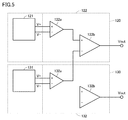
- FIG. 5 is a circuit diagram showing a circuit configuration of the current sensor according to the first embodiment of the present invention.
- the IC chip 122 of the first magnetic sensor 120 differentially amplifies the midpoint potential (V +) and the midpoint potential (V ⁇ ) of the bridge circuit of the plurality of magnetoresistive elements 121.
- a differential amplifier 122a that outputs the calculated voltage value ((V +) ⁇ (V ⁇ )) is included.
- the IC chip 132 of the second magnetic sensor 130 has a voltage value calculated by differentially amplifying the midpoint potential (V +) and the midpoint potential (V ⁇ ) of the bridge circuit of the plurality of magnetoresistive elements 131 (( A differential amplifier 132a that outputs (V +)-(V-)) is included.
- the IC chip 122 of the first magnetic sensor 120 calculates the output voltage of the bridge circuit of the plurality of magnetoresistive elements 121 and the output voltage of the bridge circuit of the bridge circuit of the plurality of magnetoresistive elements 131 by calculating the output voltage.
- a calculation unit that calculates the value of current 1 is further included.
- the IC chip 122 of the first magnetic sensor 120 has a differential amplifier 122b as a calculation unit.
- the differential amplifier 122b is connected to the differential amplifier 122a and the differential amplifier 132a. Note that a subtractor may be used as the calculation unit.
- the IC chip 132 of the second magnetic sensor 130 calculates the output voltage of the bridge circuit of the plurality of magnetoresistive elements 121 and the output voltage of the bridge circuit of the bridge circuit of the plurality of magnetoresistive elements 131 by calculating the output voltage.
- a calculation unit that can calculate the value of current 1 is further included.
- the IC chip 132 of the second magnetic sensor 130 has a differential amplifier 132b as a calculation unit. Note that a subtractor may be used as the calculation unit.
- the differential amplifier 132b is not connected to the differential amplifier 122a and the differential amplifier 132a, but instead of the differential amplifier 122b, the differential amplifier 132b is connected to the differential amplifier 122a and the differential amplifier 132a. Also good.
- the first bias magnet 140 and the second bias magnet 150 are arranged at intervals in the longitudinal direction (X-axis direction).
- the flat portion 113 is located between them, and the center 140c of the first bias magnet 140 and the second bias magnet 150 in the height direction (Z-axis direction). Is located within the range where the flat portion 113 is located in the height direction (Z-axis direction).
- each of the first bias magnet 140 and the second bias magnet 150 has a quadrangular prism shape.
- the first bias magnet 140 is disposed on the first flat portion 116.
- the second bias magnet 150 is disposed on the second flat part 117.
- Each of the first bias magnet 140 and the second bias magnet 150 is fixed to the conductor 110 by die bonding.
- the center 140c and the center 150c are intermediate between the position of the highest portion and the position of the lowest portion of each of the first bias magnet 140 and the second bias magnet 150 in the height direction (Z-axis direction). Position.
- the plurality of magnetoresistive elements 121 of the first magnetic sensor 120 and the plurality of magnetoresistive elements 131 of the second magnetic sensor 130 are located in a region sandwiched between the first bias magnet 140 and the second bias magnet 150. is doing.
- the N pole of the first bias magnet 140 and the S pole of the second bias magnet 150 are opposed to each other in the longitudinal direction (X-axis direction). Note that the S pole of the first bias magnet 140 and the N pole of the second bias magnet 150 may face each other in the longitudinal direction (X-axis direction).
- a bias magnetic field parallel to the longitudinal direction (X-axis direction) is generated between the first bias magnet 140 and the second bias magnet 150. Since the conductor 110 is made of a non-magnetic material, the bias magnetic field generated between the first bias magnet 140 and the second bias magnet 150 causes the first extending portion 114 and the second extending portion 115 to pass through. It is generated parallel to the longitudinal direction (X-axis direction).
- the plurality of magnetoresistive elements 121 of the first magnetic sensor 120 and the plurality of magnetoresistive elements 131 of the second magnetic sensor 130 are respectively interposed between the first bias magnet 140 and the second bias magnet 150.
- the generated bias magnetic field can be applied.
- each of the first bias magnet 140 and the second bias magnet 150 isotropic ferrite, anisotropic ferrite, samarium cobalt, alnico, neodymium, or the like can be used.
- Each of the first bias magnet 140 and the second bias magnet 150 may be composed of a sintered magnet or a bonded magnet.
- the conductor 110, the first magnetic sensor 120, the second magnetic sensor 130, the first bias magnet 140, and the second bias magnet 150 are integrated by the sealing resin 160.
- the sealing resin 160 a silicone resin or an epoxy resin can be used.
- the end of the conductor 110 on one side in the longitudinal direction (X-axis direction) and the end of the conductor 110 on the other side in the longitudinal direction (X-axis direction) are not covered with the sealing resin 160 and are exposed. Yes.
- connection terminals 170 and a plurality of connection terminals 171 are drawn from the sealing resin 160 in the width direction (Y-axis direction) of the conductor 110.
- the Vcc terminal is connected to the Vcc terminals of the bridge circuit of the plurality of magnetoresistive elements 121 of the first magnetic sensor 120 shown in FIG.
- the GND terminal of the plurality of connection terminals 170 is connected to the GND terminal of the bridge circuit of the plurality of magnetoresistive elements 121 of the first magnetic sensor 120 shown in FIG.
- the Vout terminal among the plurality of connection terminals 170 is connected to the Vout terminal of the IC chip 122 shown in FIG.
- the Vcc terminal of the plurality of connection terminals 171 is connected to the Vcc terminal of the bridge circuit of the plurality of magnetoresistive elements 131 of the second magnetic sensor 130 shown in FIG.
- the GND terminal of the plurality of connection terminals 171 is connected to the GND terminal of the bridge circuit of the plurality of magnetoresistive elements 131 of the second magnetic sensor 130 shown in FIG.
- the Vout terminal among the plurality of connection terminals 171 is connected to the Vout terminal of the IC chip 132 shown in FIG.
- the magnetic field 110e is generated when the current 1 to be measured flows through the flat portion 113 of the conductor 110.
- the direction of the magnetic field 110e in the width direction (Y-axis direction) of the conductor 110 is opposite to each other on the one main surface 111 side of the flat portion 113 and the other main surface 112 side of the flat portion 113. Therefore, the direction of the magnetic field 110e acting on the first magnetic sensor 120 and the direction of the magnetic field 110e acting on the second magnetic sensor 130 are opposite to each other.
- FIG. 6 shows the relationship between the output voltage ((V +) ⁇ (V ⁇ )) (mV) from each bridge circuit of the first magnetic sensor and the second magnetic sensor and the strength of the applied magnetic field (mT). It is a graph to show.
- the vertical axis represents the output voltage ((V +) ⁇ (V ⁇ )) (mV) from the bridge circuit, and the horizontal axis represents the strength of the applied magnetic field (mT).
- the output voltage from each bridge circuit of the first magnetic sensor 120 and the second magnetic sensor 130 to which a bias magnetic field is applied from the first bias magnet 140 and the second bias magnet 150 is applied. Proportional to the strength of the magnetic field.
- the first magnetic sensor 120 outputs a positive value when detecting a magnetic field directed in one direction of the detection axis 120a shown in FIG. 3, and is directed in a direction opposite to the one direction of the detection axis 120a. It has an odd function input / output characteristic that outputs a negative value when a magnetic field is detected.
- the direction of the detection axis 120a of the first magnetic sensor 120 is parallel to the width direction (Y-axis direction) of the conductor 110.
- the second magnetic sensor 130 outputs a positive value when detecting a magnetic field directed in one direction of the detection axis 130a, and detects a magnetic field directed in a direction opposite to the one direction of the detection axis 130a. In this case, it has an odd function input / output characteristic that outputs a negative value.
- the direction of the detection axis 130a of the second magnetic sensor 130 is parallel to the width direction (Y-axis direction) of the conductor 110.
- FIG. 7 is a schematic diagram showing a state in which a magnetic field generated by a current to be measured flowing through a conductor and an external magnetic field are applied to each of the first magnetic sensor and the second magnetic sensor.
- the directions of the magnetic field components in the directions are opposite to each other.
- the conductor 110 is located between the first magnetic sensor 120 and the second magnetic sensor 130, the external magnetic field source is a physical sensor. Therefore, it cannot be positioned between the first magnetic sensor 120 and the second magnetic sensor 130.
- the direction of the magnetic field component in the direction of the detection axis 120a and the external magnetic field applied to the second magnetic sensor 130 from the external magnetic field source are the same as each other.
- FIG. 8 shows the value of the current to be measured flowing through the conductor and the bridge circuit of each of the first magnetic sensor and the second magnetic sensor when an external magnetic field is applied to the first magnetic sensor and the second magnetic sensor. It is a graph which shows the relationship with an output voltage.
- the vertical axis represents the output voltage of each bridge circuit of the first magnetic sensor 120 and the second magnetic sensor 130
- the horizontal axis represents the value of the current 1 to be measured flowing through the conductor 110.
- the phase of the output voltage ( ⁇ I) of FIG. Therefore, if the output voltage ⁇ I of the bridge circuit of the first magnetic sensor 120 is a positive value, the output voltage ( ⁇ I) of the bridge circuit of the second magnetic sensor 130 is a negative value.
- the phase of the output voltage ⁇ N of the bridge circuit of the first magnetic sensor 120 and the phase of the output voltage ⁇ N of the bridge circuit of the second magnetic sensor 130 are in phase. Therefore, when the output voltage ⁇ N of the bridge circuit of the first magnetic sensor 120 is a positive value, the output voltage ⁇ N of the bridge circuit of the second magnetic sensor 130 is also a positive value.
- the output voltage from the bridge circuit of the first magnetic sensor 120 is ( ⁇ I + ⁇ N)
- the output voltage from the bridge circuit of the second magnetic sensor 130 is ( ⁇ ⁇ I + ⁇ N).
- the output voltage ( ⁇ I + ⁇ N) of the bridge circuit of the first magnetic sensor 120 and the output voltage ( ⁇ I + ⁇ N) of the bridge circuit of the second magnetic sensor 130 are calculated by the differential amplifier 122b shown in FIG. .
- FIG. 9 is a graph showing the relationship between the value of the current to be measured flowing through the conductor and the output voltage of the current sensor according to Embodiment 1 of the present invention.
- the vertical axis represents the output voltage of the current sensor 100
- the horizontal axis represents the value of the current 1 to be measured flowing through the conductor 110.
- the differential amplifier 122b As shown in FIG. 9, in the differential amplifier 122b, the difference between the output voltage ( ⁇ I + ⁇ N) of the bridge circuit of the first magnetic sensor 120 and the output voltage ( ⁇ I + ⁇ N) of the bridge circuit of the second magnetic sensor 130. Is calculated, the output voltage of the current sensor 100 becomes 2 ⁇ I. From this output voltage 2 ⁇ I, the value of the current 1 to be measured flowing through the conductor 110 is calculated. Thus, by calculating the value of the current 1 to be measured flowing through the conductor 110, the influence of the external magnetic field on the measured value of the current sensor 100 can be reduced, and the current 1 to be measured flowing through the conductor 110 can be reduced. Detection sensitivity can be increased.
- the magnetic field 110e generated by the current 1 to be measured flowing through the flat portion 113 of the conductor 110 is strongly and stable. Therefore, the first magnetic sensor 120 is disposed on one main surface 111 of the flat portion 113, and the second magnetic sensor 130 is disposed on the other main surface 112 of the flat portion 113. The stability of the measured value of the current sensor 100 can be ensured while increasing the detection sensitivity of the current 1 to be measured flowing through the conductor 110.
- the first magnetic sensor 120 disposed on the one main surface 111 side of the conductor 110 and the other main surface 112 side of the conductor 110 are disposed by a pair of bias magnets. Since a bias magnetic field can be applied to both of the second magnetic sensors 130, the current sensor 100 can be reduced in size.
- a plurality of magnetoresistive elements 121 are formed on the IC chip 122, and in the second magnetic sensor 130, a plurality of magnetoresistive elements 131 are formed on the IC chip 132, so that a current sensor is formed. 100 can be integrated with high density.
- the current sensor 100 can be easily handled. It is.
- the current sensor 200 according to the second embodiment of the present invention is mainly the current sensor according to the first embodiment in terms of the phase of the output voltage of the bridge circuit of the first magnetic sensor 120 and the second magnetic sensor 130 and the configuration of the calculation unit. Since it is different from the configuration of 100, the description of the same configuration as the current sensor 100 according to the first embodiment will not be repeated.
- FIG. 10 is a cross-sectional view showing the configuration of the current sensor according to Embodiment 2 of the present invention.
- FIG. 11 is a circuit diagram showing a circuit configuration of a current sensor according to Embodiment 2 of the present invention.
- FIG. 10 shows the same cross-sectional view as FIG.
- the first magnetic sensor 120 outputs a positive value when detecting a magnetic field directed in one direction of the detection axis 120a, and is directed in a direction opposite to the one direction of the detection axis 120a. It has an odd function input / output characteristic that outputs a negative value when a detected magnetic field is detected.
- the direction of the detection axis 120a of the first magnetic sensor 120 is parallel to the width direction (Y-axis direction) of the conductor 110.
- the second magnetic sensor 130 outputs a negative value when detecting a magnetic field directed in one direction of the detection axis 130a, and detects a magnetic field directed in a direction opposite to the one direction of the detection axis 130a. It has an odd function input / output characteristic that outputs a positive value.
- the direction of the detection axis 130a of the second magnetic sensor 130 is parallel to the width direction (Y-axis direction) of the conductor 110.
- the magnetization direction of the magnetoresistive film included in each of the plurality of magnetoresistive elements 121 and the plurality of magnetoresistive elements 131 is the application direction of the bias magnetic field applied from the first bias magnet 140 and the second bias magnet 150, and It is determined by the shape anisotropy of the magnetoresistive film. For example, when the aspect ratio of the planar shape of the magnetoresistive film is small, the influence of the shape anisotropy of the magnetoresistive film is small, and the application direction of the bias magnetic field applied from the first bias magnet 140 and the second bias magnet 150 is the main cause. Thus, the magnetization direction of the magnetoresistive film is determined. On the other hand, when the shape anisotropy of the magnetoresistive film is large, the influence of the shape anisotropy of the magnetoresistive film on the magnetization direction of the magnetoresistive film becomes large.
- the first magnetic sensor 120 and the second bias magnet 150 can be changed from the first magnetic sensor 120 and the second magnetic bias magnet 150 by changing the aspect ratios of the planar shapes of the magnetoresistive films of the plurality of magnetoresistive elements 121 and 131. Even if the application direction of the bias magnetic field applied to the second magnetic sensor 130 is the same, only the phases of the output voltages of the first magnetic sensor 120 and the second magnetic sensor 130 with respect to the magnetic field applied in the same direction are different from each other. be able to.
- the IC chip 122 of the first magnetic sensor 120 has the output voltage of the bridge circuit of the plurality of magnetoresistive elements 121 and the output voltage of the bridge circuit of the bridge circuit of the plurality of magnetoresistive elements 131, It has a calculation part which calculates the value of current 1 to be measured by calculation.
- the IC chip 122 of the first magnetic sensor 120 has a summing amplifier 222b as a calculation unit.
- the summing amplifier 222b is connected to the differential amplifier 122a and the differential amplifier 132a.
- An adder may be used as the calculation unit.
- the IC chip 132 of the second magnetic sensor 130 calculates the output voltage of the bridge circuit of the plurality of magnetoresistive elements 121 and the output voltage of the bridge circuit of the bridge circuit of the plurality of magnetoresistive elements 131 by calculating the output voltage.
- a calculation unit that can calculate the value of current 1 is further included.
- the IC chip 132 of the second magnetic sensor 130 has a summing amplifier 232b as a calculation unit. An adder may be used as the calculation unit.
- the summing amplifier 232b is not connected to the differential amplifier 122a and the differential amplifier 132a, the summing amplifier 232b may be connected to the differential amplifier 122a and the differential amplifier 132a instead of the summing amplifier 222b.
- the phase of the output voltage ⁇ I of the bridge circuit of the first magnetic sensor 120 and the bridge circuit of the second magnetic sensor 130 are in phase. Therefore, when the output voltage ⁇ I of the bridge circuit of the first magnetic sensor 120 is a positive value, the output voltage ⁇ I of the bridge circuit of the second magnetic sensor 130 is also a positive value.
- the phase of the output voltage ⁇ N of the bridge circuit of the first magnetic sensor 120 is opposite to the phase of the output voltage ( ⁇ N) of the bridge circuit of the second magnetic sensor 130. . Therefore, if the output voltage ⁇ N of the bridge circuit of the first magnetic sensor 120 is a positive value, the output voltage ( ⁇ N) of the bridge circuit of the second magnetic sensor 130 is a negative value.
- the output voltage from the bridge circuit of the first magnetic sensor 120 is ( ⁇ I + ⁇ N)
- the output voltage from the bridge circuit of the second magnetic sensor 130 is ( ⁇ I + ( ⁇ ⁇ N)).
- the output voltage ( ⁇ I + ⁇ N) of the bridge circuit of the first magnetic sensor 120 and the output voltage ( ⁇ I + ( ⁇ ⁇ N)) of the bridge circuit of the second magnetic sensor 130 are calculated by the addition amplifier 222b shown in FIG.
- the addition amplifier 222b shown in FIG.
- the output voltage ( ⁇ I + ⁇ N) of the bridge circuit of the first magnetic sensor 120 and the output voltage ( ⁇ I + ( ⁇ ⁇ N)) of the bridge circuit of the second magnetic sensor 130 are added, thereby obtaining a current.
- the output voltage of the sensor 200 is 2 ⁇ I. From this output voltage 2 ⁇ I, the value of the current 1 to be measured flowing through the conductor 110 is calculated.
- the influence of the external magnetic field on the measured value of the current sensor 200 can be reduced, and the current 1 to be measured flowing through the conductor 110 can be reduced. Detection sensitivity can be increased.
Landscapes
- Physics & Mathematics (AREA)
- General Physics & Mathematics (AREA)
- Measuring Magnetic Variables (AREA)
- Measuring Instrument Details And Bridges, And Automatic Balancing Devices (AREA)
Abstract
Dans la présente invention, une paire d'aimants de polarisation (140, 150) applique un champ magnétique de polarisation à un premier capteur magnétique (120) et à un second capteur magnétique (130). Un conducteur (110) comprend une partie plate (113) qui s'étend dans la direction longitudinale, et une paire de parties d'extension (114, 115) qui s'étend à partir des deux extrémités longitudinales de la partie plate (113) et qui est pliée vers un côté de surface principale (112). Le premier capteur magnétique (120) et le second capteur magnétique (130) sont chacun positionnés le long de la partie plate (113). La partie plate (113) est positionnée entre la paire d'aimants de polarisation (140, 150), et les centres respectifs (140c, 150c) de la paire d'aimants de polarisation (140, 150), dans une direction de hauteur qui est orthogonale à l'autre surface principale (111) de la partie plate (113), sont positionnés dans la plage dans laquelle la partie plate (113) est positionnée dans la direction de la hauteur.
Applications Claiming Priority (2)
| Application Number | Priority Date | Filing Date | Title |
|---|---|---|---|
| JP2016-223110 | 2016-11-16 | ||
| JP2016223110 | 2016-11-16 |
Publications (1)
| Publication Number | Publication Date |
|---|---|
| WO2018092580A1 true WO2018092580A1 (fr) | 2018-05-24 |
Family
ID=62146261
Family Applications (1)
| Application Number | Title | Priority Date | Filing Date |
|---|---|---|---|
| PCT/JP2017/039307 Ceased WO2018092580A1 (fr) | 2016-11-16 | 2017-10-31 | Capteur de courant |
Country Status (1)
| Country | Link |
|---|---|
| WO (1) | WO2018092580A1 (fr) |
Cited By (1)
| Publication number | Priority date | Publication date | Assignee | Title |
|---|---|---|---|---|
| TWI769819B (zh) * | 2021-05-18 | 2022-07-01 | 宇能電科技股份有限公司 | 電流感測器與裝置 |
Citations (3)
| Publication number | Priority date | Publication date | Assignee | Title |
|---|---|---|---|---|
| US4841235A (en) * | 1987-06-11 | 1989-06-20 | Eaton Corporation | MRS current sensor |
| JP2011089931A (ja) * | 2009-10-23 | 2011-05-06 | Denso Corp | 電流センサ |
| JP2015155796A (ja) * | 2012-05-31 | 2015-08-27 | パナソニック株式会社 | 電流センサ |
-
2017
- 2017-10-31 WO PCT/JP2017/039307 patent/WO2018092580A1/fr not_active Ceased
Patent Citations (3)
| Publication number | Priority date | Publication date | Assignee | Title |
|---|---|---|---|---|
| US4841235A (en) * | 1987-06-11 | 1989-06-20 | Eaton Corporation | MRS current sensor |
| JP2011089931A (ja) * | 2009-10-23 | 2011-05-06 | Denso Corp | 電流センサ |
| JP2015155796A (ja) * | 2012-05-31 | 2015-08-27 | パナソニック株式会社 | 電流センサ |
Cited By (1)
| Publication number | Priority date | Publication date | Assignee | Title |
|---|---|---|---|---|
| TWI769819B (zh) * | 2021-05-18 | 2022-07-01 | 宇能電科技股份有限公司 | 電流感測器與裝置 |
Similar Documents
| Publication | Publication Date | Title |
|---|---|---|
| JP5867235B2 (ja) | 磁気センサ装置 | |
| US10184959B2 (en) | Magnetic current sensor and current measurement method | |
| JP5271448B2 (ja) | 磁気式位置検出装置 | |
| CN108713148B (zh) | 电流传感器以及电流传感器模块 | |
| US7642773B2 (en) | Magnetic sensor, production method thereof, rotation detection device, and position detection device | |
| JP6409970B2 (ja) | 電流センサ | |
| CN104297548B (zh) | 电流传感器 | |
| JP6427588B2 (ja) | 磁気センサ | |
| CN101395450A (zh) | 磁传感器装置、磁编码器装置及磁尺的制造方法 | |
| JP5899012B2 (ja) | 磁気センサ | |
| CN107430155A (zh) | 电流传感器 | |
| JP7070532B2 (ja) | 磁気センサ | |
| CN107615078A (zh) | 电流传感器 | |
| JP6671985B2 (ja) | 電流センサ | |
| JP2013044641A (ja) | 磁気センサ | |
| JP6384677B2 (ja) | 電流センサ | |
| JP6555421B2 (ja) | 磁気センサおよびそれを備えた電流センサ | |
| JPWO2016203781A1 (ja) | 電流センサ | |
| JP2014089088A (ja) | 磁気抵抗効果素子 | |
| JP6671986B2 (ja) | 電流センサおよびその製造方法 | |
| WO2011074488A1 (fr) | Capteur magnétique | |
| JP5849914B2 (ja) | 電流センサ | |
| WO2018092580A1 (fr) | Capteur de courant | |
| WO2015125699A1 (fr) | Capteur magnétique | |
| JP2010243232A (ja) | 電流センサ |
Legal Events
| Date | Code | Title | Description |
|---|---|---|---|
| 121 | Ep: the epo has been informed by wipo that ep was designated in this application |
Ref document number: 17871506 Country of ref document: EP Kind code of ref document: A1 |
|
| NENP | Non-entry into the national phase |
Ref country code: DE |
|
| 122 | Ep: pct application non-entry in european phase |
Ref document number: 17871506 Country of ref document: EP Kind code of ref document: A1 |
|
| NENP | Non-entry into the national phase |
Ref country code: JP |